JP4662494B2 - Liquid crystal display device - Google Patents
Liquid crystal display device Download PDFInfo
- Publication number
- JP4662494B2 JP4662494B2 JP2007269433A JP2007269433A JP4662494B2 JP 4662494 B2 JP4662494 B2 JP 4662494B2 JP 2007269433 A JP2007269433 A JP 2007269433A JP 2007269433 A JP2007269433 A JP 2007269433A JP 4662494 B2 JP4662494 B2 JP 4662494B2
- Authority
- JP
- Japan
- Prior art keywords
- pixel
- liquid crystal
- signal line
- electrode
- potential
- Prior art date
- Legal status (The legal status is an assumption and is not a legal conclusion. Google has not performed a legal analysis and makes no representation as to the accuracy of the status listed.)
- Active
Links
- 239000004973 liquid crystal related substance Substances 0.000 title claims description 77
- 239000000758 substrate Substances 0.000 claims description 44
- 239000010410 layer Substances 0.000 claims description 25
- 230000005684 electric field Effects 0.000 claims description 23
- 239000011229 interlayer Substances 0.000 claims description 19
- 239000003990 capacitor Substances 0.000 claims description 10
- 239000010408 film Substances 0.000 description 39
- 230000003287 optical effect Effects 0.000 description 7
- 239000011159 matrix material Substances 0.000 description 6
- 238000000034 method Methods 0.000 description 6
- 239000011347 resin Substances 0.000 description 6
- 229920005989 resin Polymers 0.000 description 6
- 239000004065 semiconductor Substances 0.000 description 6
- 238000010586 diagram Methods 0.000 description 5
- 239000010409 thin film Substances 0.000 description 5
- 238000002834 transmittance Methods 0.000 description 4
- 229910021420 polycrystalline silicon Inorganic materials 0.000 description 3
- 229920005591 polysilicon Polymers 0.000 description 3
- VYPSYNLAJGMNEJ-UHFFFAOYSA-N silicon dioxide Inorganic materials O=[Si]=O VYPSYNLAJGMNEJ-UHFFFAOYSA-N 0.000 description 3
- 229910021417 amorphous silicon Inorganic materials 0.000 description 2
- 239000003086 colorant Substances 0.000 description 2
- 239000011521 glass Substances 0.000 description 2
- 229910010272 inorganic material Inorganic materials 0.000 description 2
- 239000011147 inorganic material Substances 0.000 description 2
- 239000000463 material Substances 0.000 description 2
- 230000000149 penetrating effect Effects 0.000 description 2
- 230000010287 polarization Effects 0.000 description 2
- 239000010453 quartz Substances 0.000 description 2
- 125000006850 spacer group Chemical group 0.000 description 2
- 229910052581 Si3N4 Inorganic materials 0.000 description 1
- 239000004020 conductor Substances 0.000 description 1
- 239000000470 constituent Substances 0.000 description 1
- 230000008878 coupling Effects 0.000 description 1
- 238000010168 coupling process Methods 0.000 description 1
- 238000005859 coupling reaction Methods 0.000 description 1
- AMGQUBHHOARCQH-UHFFFAOYSA-N indium;oxotin Chemical compound [In].[Sn]=O AMGQUBHHOARCQH-UHFFFAOYSA-N 0.000 description 1
- 239000000203 mixture Substances 0.000 description 1
- 150000004767 nitrides Chemical class 0.000 description 1
- 239000011368 organic material Substances 0.000 description 1
- 230000003071 parasitic effect Effects 0.000 description 1
- 238000005192 partition Methods 0.000 description 1
- 230000001105 regulatory effect Effects 0.000 description 1
- 230000000717 retained effect Effects 0.000 description 1
- HQVNEWCFYHHQES-UHFFFAOYSA-N silicon nitride Chemical compound N12[Si]34N5[Si]62N3[Si]51N64 HQVNEWCFYHHQES-UHFFFAOYSA-N 0.000 description 1
- 229910052814 silicon oxide Inorganic materials 0.000 description 1
- YVTHLONGBIQYBO-UHFFFAOYSA-N zinc indium(3+) oxygen(2-) Chemical compound [O--].[Zn++].[In+3] YVTHLONGBIQYBO-UHFFFAOYSA-N 0.000 description 1
Images


Classifications
-
- G—PHYSICS
- G02—OPTICS
- G02F—OPTICAL DEVICES OR ARRANGEMENTS FOR THE CONTROL OF LIGHT BY MODIFICATION OF THE OPTICAL PROPERTIES OF THE MEDIA OF THE ELEMENTS INVOLVED THEREIN; NON-LINEAR OPTICS; FREQUENCY-CHANGING OF LIGHT; OPTICAL LOGIC ELEMENTS; OPTICAL ANALOGUE/DIGITAL CONVERTERS
- G02F1/00—Devices or arrangements for the control of the intensity, colour, phase, polarisation or direction of light arriving from an independent light source, e.g. switching, gating or modulating; Non-linear optics
- G02F1/01—Devices or arrangements for the control of the intensity, colour, phase, polarisation or direction of light arriving from an independent light source, e.g. switching, gating or modulating; Non-linear optics for the control of the intensity, phase, polarisation or colour
- G02F1/13—Devices or arrangements for the control of the intensity, colour, phase, polarisation or direction of light arriving from an independent light source, e.g. switching, gating or modulating; Non-linear optics for the control of the intensity, phase, polarisation or colour based on liquid crystals, e.g. single liquid crystal display cells
- G02F1/133—Constructional arrangements; Operation of liquid crystal cells; Circuit arrangements
- G02F1/1333—Constructional arrangements; Manufacturing methods
- G02F1/1343—Electrodes
- G02F1/134309—Electrodes characterised by their geometrical arrangement
- G02F1/134363—Electrodes characterised by their geometrical arrangement for applying an electric field parallel to the substrate, i.e. in-plane switching [IPS]
-
- G—PHYSICS
- G02—OPTICS
- G02F—OPTICAL DEVICES OR ARRANGEMENTS FOR THE CONTROL OF LIGHT BY MODIFICATION OF THE OPTICAL PROPERTIES OF THE MEDIA OF THE ELEMENTS INVOLVED THEREIN; NON-LINEAR OPTICS; FREQUENCY-CHANGING OF LIGHT; OPTICAL LOGIC ELEMENTS; OPTICAL ANALOGUE/DIGITAL CONVERTERS
- G02F1/00—Devices or arrangements for the control of the intensity, colour, phase, polarisation or direction of light arriving from an independent light source, e.g. switching, gating or modulating; Non-linear optics
- G02F1/01—Devices or arrangements for the control of the intensity, colour, phase, polarisation or direction of light arriving from an independent light source, e.g. switching, gating or modulating; Non-linear optics for the control of the intensity, phase, polarisation or colour
- G02F1/13—Devices or arrangements for the control of the intensity, colour, phase, polarisation or direction of light arriving from an independent light source, e.g. switching, gating or modulating; Non-linear optics for the control of the intensity, phase, polarisation or colour based on liquid crystals, e.g. single liquid crystal display cells
- G02F1/133—Constructional arrangements; Operation of liquid crystal cells; Circuit arrangements
- G02F1/136—Liquid crystal cells structurally associated with a semi-conducting layer or substrate, e.g. cells forming part of an integrated circuit
- G02F1/1362—Active matrix addressed cells
- G02F1/136213—Storage capacitors associated with the pixel electrode
-
- G—PHYSICS
- G09—EDUCATION; CRYPTOGRAPHY; DISPLAY; ADVERTISING; SEALS
- G09G—ARRANGEMENTS OR CIRCUITS FOR CONTROL OF INDICATING DEVICES USING STATIC MEANS TO PRESENT VARIABLE INFORMATION
- G09G3/00—Control arrangements or circuits, of interest only in connection with visual indicators other than cathode-ray tubes
- G09G3/20—Control arrangements or circuits, of interest only in connection with visual indicators other than cathode-ray tubes for presentation of an assembly of a number of characters, e.g. a page, by composing the assembly by combination of individual elements arranged in a matrix no fixed position being assigned to or needed to be assigned to the individual characters or partial characters
- G09G3/34—Control arrangements or circuits, of interest only in connection with visual indicators other than cathode-ray tubes for presentation of an assembly of a number of characters, e.g. a page, by composing the assembly by combination of individual elements arranged in a matrix no fixed position being assigned to or needed to be assigned to the individual characters or partial characters by control of light from an independent source
- G09G3/36—Control arrangements or circuits, of interest only in connection with visual indicators other than cathode-ray tubes for presentation of an assembly of a number of characters, e.g. a page, by composing the assembly by combination of individual elements arranged in a matrix no fixed position being assigned to or needed to be assigned to the individual characters or partial characters by control of light from an independent source using liquid crystals
- G09G3/3611—Control of matrices with row and column drivers
- G09G3/3648—Control of matrices with row and column drivers using an active matrix
-
- G—PHYSICS
- G09—EDUCATION; CRYPTOGRAPHY; DISPLAY; ADVERTISING; SEALS
- G09G—ARRANGEMENTS OR CIRCUITS FOR CONTROL OF INDICATING DEVICES USING STATIC MEANS TO PRESENT VARIABLE INFORMATION
- G09G2300/00—Aspects of the constitution of display devices
- G09G2300/04—Structural and physical details of display devices
- G09G2300/0421—Structural details of the set of electrodes
- G09G2300/0426—Layout of electrodes and connections
-
- G—PHYSICS
- G09—EDUCATION; CRYPTOGRAPHY; DISPLAY; ADVERTISING; SEALS
- G09G—ARRANGEMENTS OR CIRCUITS FOR CONTROL OF INDICATING DEVICES USING STATIC MEANS TO PRESENT VARIABLE INFORMATION
- G09G2300/00—Aspects of the constitution of display devices
- G09G2300/04—Structural and physical details of display devices
- G09G2300/0439—Pixel structures
- G09G2300/0465—Improved aperture ratio, e.g. by size reduction of the pixel circuit, e.g. for improving the pixel density or the maximum displayable luminance or brightness
Description
この発明は、液晶表示装置に係り、特に、液晶表示パネルを構成する一方の基板に層間絶縁膜を介して対向する一対の電極を備えた構造の液晶表示装置に関する。 The present invention relates to a liquid crystal display device, and more particularly to a liquid crystal display device having a structure including a pair of electrodes facing each other through an interlayer insulating film on one substrate constituting a liquid crystal display panel.
近年、平面表示装置が盛んに開発されており、中でも液晶表示装置は、軽量、薄型、低消費電力等の利点から特に注目を集めている。特に、各画素にスイッチング素子を組み込んだアクティブマトリクス型液晶表示装置においては、IPS(In−Plane Switching)モードやFFS(Fringe Field Switching)モードなどの横電界(フリンジ電界も含む)を主として利用した構造が注目されている。(例えば、特許文献1及び特許文献2参照)。
2. Description of the Related Art In recent years, flat display devices have been actively developed. In particular, liquid crystal display devices have attracted particular attention because of their advantages such as light weight, thinness, and low power consumption. In particular, in an active matrix liquid crystal display device in which a switching element is incorporated in each pixel, a structure that mainly uses a lateral electric field (including a fringe electric field) such as an IPS (In-Plane Switching) mode or an FFS (Fringe Field Switching) mode. Is attracting attention. (For example, refer to
このIPSモードやFFSモードの液晶表示装置は、アレイ基板に形成された画素電極とコモン電極とを備え、アレイ基板の主面に対してほぼ平行な横電界で液晶分子をスイッチングする。また、アレイ基板及び対向基板のそれぞれの外面には、互いに偏光軸が直交するように配置された偏光板が配置されている。このような偏光板の配置により、例えば電圧無印加時に黒色画面を表示し、映像信号に対応した電圧を画素電極に印加することにより徐々に透過率(変調率)が増加して白色画面を表示する。このような液晶表示装置では、液晶分子が基板主面とほぼ平行な平面内で回転するため、透過光の入射方向に対して偏光状態が大きく影響しないので、視野角依存性は小さく、広い視野角特性を有するといった特徴がある。 This IPS mode or FFS mode liquid crystal display device includes a pixel electrode and a common electrode formed on an array substrate, and switches liquid crystal molecules with a lateral electric field substantially parallel to the main surface of the array substrate. In addition, polarizing plates are arranged on the outer surfaces of the array substrate and the counter substrate so that the polarization axes are orthogonal to each other. With such a polarizing plate arrangement, for example, a black screen is displayed when no voltage is applied, and a white screen is displayed by gradually increasing the transmittance (modulation factor) by applying a voltage corresponding to the video signal to the pixel electrode. To do. In such a liquid crystal display device, since the liquid crystal molecules rotate in a plane substantially parallel to the main surface of the substrate, the polarization state does not greatly affect the incident direction of transmitted light, so the viewing angle dependency is small and a wide field of view. There is a feature of having angular characteristics.
特許文献3によれば、IPS方式において、画素への書込が終わった後の信号線電位の変化により発生する電界及び隣接する信号線の電位の変化による電界によって表示が影響を受けるといった課題に対して、この表示への影響を防止するための配線を配置することなく、信号線と画素電極とを共用化することにより、広い画素部面積を確保する技術が開示されている。
According to
特許文献4によれば、各走査信号線に印加される電圧が選択走査電圧から非選択走査電圧に変化したときに各画素の画素電圧に電位変動が生じないようにする技術が開示されており、特に、IPS方式の液晶表示モジュールにおいては、画素電極に印加される階調電圧の最大振幅レベルを小さくするための技術が開示されている。
横電界を主として利用した液晶モードにおいては、信号線からの表示に影響を与える電界を遮蔽するとともに不所望な寄生容量を抑制し、表示品位を改善することが望まれている。 In a liquid crystal mode mainly using a lateral electric field, it is desired to improve display quality by shielding an electric field that affects display from a signal line and suppressing unwanted parasitic capacitance.
この発明は、上述した問題点に鑑みなされたものであって、その目的は、画素開口率の低下を招くことなく表示品位の良好な画像を表示可能な液晶表示装置を提供することにある。 The present invention has been made in view of the above-described problems, and an object of the present invention is to provide a liquid crystal display device capable of displaying an image with good display quality without causing a decrease in pixel aperture ratio.
この発明の態様による液晶表示装置は、
一対の基板間に液晶層を保持し、一方の基板が層間絶縁膜を介して対向する一対の第1電極及び第2電極を備えた構成の横電界モードの液晶表示装置であって、
マトリクス状の画素の行方向に延在する走査線と、
前記画素の列方向に延在する信号線と、
各画素において、隣接する信号線間に形成された蓄積容量素子と、
各画素に配置されたスイッチング素子と、
を備え、行方向に隣接する一対の信号線間の画素は、前記スイッチング素子を介して一方の信号線に接続された前記第1電極と、他方の信号線に接続された前記第2電極と、を有することにより、隣接する一対の信号線間に前記蓄積容量素子を形成したことを特徴とする。
A liquid crystal display device according to an aspect of the present invention includes:
A lateral electric field mode liquid crystal display device having a configuration in which a liquid crystal layer is held between a pair of substrates, and one substrate includes a pair of first and second electrodes facing each other with an interlayer insulating film therebetween.
A scanning line extending in the row direction of the matrix-shaped pixels;
A signal line extending in the column direction of the pixels;
In each pixel, a storage capacitor element formed between adjacent signal lines;
A switching element disposed in each pixel;
A pixel between a pair of signal lines adjacent in the row direction includes: the first electrode connected to one signal line via the switching element; and the second electrode connected to the other signal line. The storage capacitor element is formed between a pair of adjacent signal lines.
この発明によれば、画素開口率の低下を招くことなく表示品位の良好な画像を表示可能な液晶表示装置を提供することができる。 According to the present invention, it is possible to provide a liquid crystal display device capable of displaying an image with good display quality without causing a decrease in pixel aperture ratio.
以下、この発明の一実施の形態に係る液晶表示装置について図面を参照して説明する。 A liquid crystal display device according to an embodiment of the present invention will be described below with reference to the drawings.
ここでは、一方の基板に一対の電極を備え、これらの間に形成される横電界(基板面に略平行な水平電界)を主として利用して液晶分子をスイッチングする液晶モードとして、FFSモードの液晶表示装置を例に説明する。 Here, an FFS mode liquid crystal is provided as a liquid crystal mode in which a pair of electrodes is provided on one substrate, and liquid crystal molecules are switched using mainly a lateral electric field (horizontal electric field substantially parallel to the substrate surface) formed between the electrodes. A display device will be described as an example.
図1及び図2に示すように、液晶表示装置は、アクティブマトリクスタイプの液晶表示装置であって、液晶表示パネルLPNを備えている。この液晶表示パネルLPNは、アレイ基板ARと、このアレイ基板ARと互いに対向して配置された対向基板CTと、これらのアレイ基板ARと対向基板CTとの間に保持された液晶層LQと、を備えて構成されている。このような液晶表示パネルLPNは、画像を表示するアクティブエリアDSPを備えている。このアクティブエリアDSPは、m×n個(m及びnを自然数である)のマトリクス状に配置された画素PXによって構成されている。 As shown in FIGS. 1 and 2, the liquid crystal display device is an active matrix type liquid crystal display device and includes a liquid crystal display panel LPN. The liquid crystal display panel LPN includes an array substrate AR, a counter substrate CT arranged to face the array substrate AR, a liquid crystal layer LQ held between the array substrate AR and the counter substrate CT, It is configured with. Such a liquid crystal display panel LPN includes an active area DSP for displaying an image. The active area DSP is composed of m × n pixels (m and n are natural numbers) arranged in a matrix PX.
この実施の形態においては、透過型の液晶表示パネルLPNを備えた液晶表示装置について説明するが、本発明は透過型に限定されるものではなく、反射型に適用しても良い。透過型の液晶表示装置は、液晶表示パネルLPNに対してアレイ基板AR側に配置されたバックライトユニットBLを備えている。このような透過型の液晶表示パネルLPNを備えた液晶表示装置は、バックライトユニットBLからのバックライト光を選択的に透過することによって画像を表示するように構成されている。 In this embodiment, a liquid crystal display device including a transmissive liquid crystal display panel LPN will be described. However, the present invention is not limited to a transmissive type, and may be applied to a reflective type. The transmissive liquid crystal display device includes a backlight unit BL disposed on the array substrate AR side with respect to the liquid crystal display panel LPN. A liquid crystal display device including such a transmissive liquid crystal display panel LPN is configured to display an image by selectively transmitting backlight light from the backlight unit BL.
より具体的な液晶表示装置の構成について説明する。 A more specific configuration of the liquid crystal display device will be described.
アレイ基板ARは、ガラス板や石英板などの光透過性を有する絶縁基板10を用いて形成されている。すなわち、このアレイ基板ARは、アクティブエリアDSPにおいて、画素PX毎に配置されたm×n個の第1電極E1、各画素PXの行方向Hにそれぞれ延在するn本の走査線Y(Y1〜Yn)、各画素PXの列方向Vにそれぞれ延在する少なくとも(m+1)本の信号線X(X1〜X(m+1))、各画素PXにおいて走査線Yと信号線Xとの交差部を含む領域に配置されたm×n個のスイッチング素子W、画素PX毎に配置されたm×n個の第2電極E2などを備えている。アレイ基板ARの液晶層LQに接触する面は、配向膜20によって覆われている。
The array substrate AR is formed using an
各スイッチング素子Wは、例えば、nチャネル薄膜トランジスタであり、絶縁基板10の上に配置された半導体層12を備えている。この半導体層12は、例えば、ポリシリコンやアモルファスシリコンなどによって形成可能であり、ここではポリシリコンによって形成されている。半導体層12は、チャネル領域12Cを挟んだ両側にそれぞれソース領域12S及びドレイン領域12Dを有している。この半導体層12は、ゲート絶縁膜14によって覆われている。
Each switching element W is, for example, an n-channel thin film transistor, and includes a semiconductor layer 12 disposed on the
スイッチング素子Wのゲート電極WGは、走査線Yに接続されている(あるいは走査線Yと一体的に形成されている)。ゲート電極WG及び走査線Yは、ともにゲート絶縁膜14上に配置されている。これらのゲート電極WG及び走査線Yは、第1層間絶縁膜16によって覆われている。ゲート絶縁膜14及び第1層間絶縁膜16は、酸化シリコン膜や窒化シリコン膜などの無機系材料からなる薄膜によって形成可能である。
The gate electrode WG of the switching element W is connected to the scanning line Y (or formed integrally with the scanning line Y). Both the gate electrode WG and the scanning line Y are disposed on the
スイッチング素子Wのソース電極WS及びドレイン電極WDは、第1層間絶縁膜16上においてゲート電極WGの両側に配置されている。ソース電極WSは、信号線Xに接続される(あるいは信号線Xと一体に形成される)とともに、ゲート絶縁膜14及び第1層間絶縁膜16を貫通するコンタクトホールを介して半導体層12のソース領域12Sにコンタクトしている。ドレイン電極WDは、第1電極E1に接続される(あるいは第1電極E1と一体に形成される)とともに、ゲート絶縁膜14及び第1層間絶縁膜16を貫通するコンタクトホールを介して半導体層12のドレイン領域12Dにコンタクトしている。これらのソース電極WS、ドレイン電極WD、及び、信号線Xは、第2層間絶縁膜18によって覆われている。
The source electrode WS and the drain electrode WD of the switching element W are disposed on both sides of the gate electrode WG on the first
上述したような構成のポリシリコン薄膜トランジスタを適用した場合においては、第2層間絶縁膜18は、有機系材料(樹脂材料)によって形成可能である。なお、アモルファスシリコン薄膜トランジスタを適用した場合においては、第2層間絶縁膜18は、窒化膜などの無機系材料からなる薄膜によって形成可能である。
When the polysilicon thin film transistor having the above-described configuration is applied, the second
n本の走査線Y(Y1〜Yn)は、それぞれ列方向Vに並んで配置されている。(m+1)本の信号線X(X1〜X(m+1))は、それぞれ行方向Hに並んで配置されている。つまり、m×n個の画素PXのそれぞれは、行方向に隣接する一対の信号線Xの間に位置している。 The n scanning lines Y (Y1 to Yn) are arranged in the column direction V, respectively. (M + 1) signal lines X (X1 to X (m + 1)) are arranged in the row direction H, respectively. That is, each of the m × n pixels PX is located between a pair of signal lines X adjacent in the row direction.
各画素PXにおいて、第1電極E1と第2電極E2とは、層間絶縁膜を介して対向している。これらの第1電極E1及び第2電極E2は、隣接する信号線間に形成された蓄積容量素子としての機能を有している。 In each pixel PX, the first electrode E1 and the second electrode E2 are opposed to each other through an interlayer insulating film. The first electrode E1 and the second electrode E2 have a function as a storage capacitor formed between adjacent signal lines.
図2に示した例では、第1電極E1と第2電極E2とは、第2層間絶縁膜18を介して対向している。すなわち、第1電極E1は、第2層間絶縁膜18上において島状に配置され、画素PXの両側に配置された一対の信号線のうちの一方の信号線XAに接続されている。第2電極E2は、第2層間絶縁膜18の下、つまり第1層間絶縁膜16と第2層間絶縁膜18との間において島状に配置され、画素PXの両側に配置された一対の信号線のうちの他方の信号線XBに接続されている。
In the example shown in FIG. 2, the first electrode E1 and the second electrode E2 are opposed to each other with the second
ここでは、第1電極E1は、第2層間絶縁膜18を貫通するコンタクトホールを介してドレイン電極WDと電気的に接続されており、各画素PXのスイッチング素子Wを介して信号線XAに接続されている。また、第2電極E2は、第1電極E1が接続された信号線XAに対して行方向Hに隣接する信号線XBに接続されている。すなわち、第2電極E2のエッジが隣接信号線XBに重なって、両者が電気的に接続されている。このような構成によれば、第1電極E1及び第2電極E2は、両者の間に液晶容量Clcを形成するとともに、これを保持するための補助容量Csを形成する蓄積容量素子としての機能を兼ね備えている。
Here, the first electrode E1 is electrically connected to the drain electrode WD via a contact hole penetrating the second
これらの第1電極E1及び第2電極E2は、例えばインジウム・ティン・オキサイド(ITO)やインジウム・ジンク・オキサイド(IZO)などの光透過性を有する導電材料によって形成されている。 The first electrode E1 and the second electrode E2 are formed of a light-transmitting conductive material such as indium tin oxide (ITO) or indium zinc oxide (IZO).
アレイ基板ARは、さらに、アクティブエリアDSPの周辺の駆動回路領域DCTにおいて、n本の走査線Yに接続された走査線ドライバYDを構成する少なくとも一部や、(m+1)本の信号線Xに接続された信号線ドライバXDを構成する少なくとも一部などを備えている。走査線ドライバYDは、コントローラCNTによる制御に基づいてn本の走査線Yに順次走査信号(駆動信号)を供給する。また、信号線ドライバXDは、コントローラCNTによる制御に基づいて各行のスイッチング素子Wが走査信号によってオンするタイミングで(m+1)本の信号線Xに映像信号(駆動信号)を供給する。 The array substrate AR further includes at least part of the scanning line driver YD connected to the n scanning lines Y and (m + 1) signal lines X in the driving circuit region DCT around the active area DSP. At least a part of the connected signal line driver XD is included. The scanning line driver YD sequentially supplies scanning signals (driving signals) to the n scanning lines Y based on control by the controller CNT. Further, the signal line driver XD supplies video signals (drive signals) to the (m + 1) signal lines X at a timing when the switching elements W in each row are turned on by the scanning signal based on the control by the controller CNT.
信号線ドライバXDは、各行のそれぞれの画素PXについて、所定の画素電位に設定する電位設定部としての機能を有している。すなわち、信号線ドライバXDは、各信号線Xに映像信号を供給する際、各画素PXについて、一方の信号線の電位が他方の信号線の電位を基準とした画素電位に設定されるような信号電圧を出力する。 The signal line driver XD has a function as a potential setting unit that sets a predetermined pixel potential for each pixel PX in each row. That is, when the signal line driver XD supplies a video signal to each signal line X, for each pixel PX, the potential of one signal line is set to a pixel potential based on the potential of the other signal line. Outputs signal voltage.
一方、対向基板CTは、ガラス板や石英板などの光透過性を有する絶縁基板30を用いて形成されている。特に、カラー表示タイプの液晶表示装置においては、図2に示したように、対向基板CTは、絶縁基板30の内面すなわち液晶層LQに対向する面に、各画素PXを区画するブラックマトリクス32、ブラックマトリクス32によって囲まれた各画素PXに個別に配置されたカラーフィルタ層34などを備えている。なお、カラーフィルタ層34は、アレイ基板AR側に配置されても良い。また、対向基板CTは、さらに、外部電界の影響を緩和するためのシールド電極や、カラーフィルタ層34の表面の凹凸を平坦化するように比較的厚い膜厚で配置されたオーバコート層などを備えて構成してもよい。
On the other hand, the counter substrate CT is formed using an insulating
ブラックマトリクス32は、絶縁基板30上において、アレイ基板ARに設けられた走査線Yや信号線X、スイッチング素子Wなどの配線部に対向するように配置されている。カラーフィルタ層34は、絶縁基板30上に配置され、互いに異なる複数の色、例えば赤色、青色、緑色といった3原色にそれぞれ着色された着色樹脂によって形成されている。赤色着色樹脂、青色着色樹脂、及び、緑色着色樹脂は、それぞれ赤色画素、青色画素、及び、緑色画素に対応して配置されている。対向基板CTの液晶層LQに接触する面は、配向膜36によって覆われている。
The
上述したような構成のアレイ基板ARと対向基板CTとをそれぞれの配向膜20及び配向膜36が対向するように配置したとき、両者の間に配置された図示しないスペーサ(例えば、樹脂材料によって形成された柱状スペーサ)により、所定のギャップが形成される。液晶層LQは、これらのアレイ基板ARの配向膜20と対向基板CTの配向膜36との間に形成されたギャップに封入された液晶分子40を含む液晶組成物によって構成されている。
When the array substrate AR and the counter substrate CT configured as described above are arranged so that the
液晶層LQに含まれる液晶分子40は、配向膜20及び配向膜36による規制力によって配向されている。すなわち、第1電極E1の電位と第2電極E2の電位との間に電位差が形成されていない(つまり、第1電極E1と第2電極E2との間に電界が形成されていない)無電界時には、液晶分子40は、その長軸が配向膜20及び配向膜36のラビング方向と平行な方位を向くように配向されている。
The
また、この液晶表示装置は、液晶表示パネルLPNの一方の外面(すなわちアレイ基板ARの液晶層LQと接触する面とは反対の面)に設けられた光学素子OD1を備え、また、液晶表示パネルLPNの他方の外面(すなわち対向基板CTの液晶層LQと接触する面と反対の面)に設けられた光学素子OD2を備えている。 In addition, the liquid crystal display device includes an optical element OD1 provided on one outer surface of the liquid crystal display panel LPN (that is, the surface opposite to the surface in contact with the liquid crystal layer LQ of the array substrate AR), and the liquid crystal display panel An optical element OD2 provided on the other outer surface of the LPN (that is, the surface opposite to the surface in contact with the liquid crystal layer LQ of the counter substrate CT) is provided.
これらの光学素子OD1及びOD2は、偏光板を含み、例えば、無電界時において、液晶表示パネルLPNの透過率が最低となる(つまり黒色画面を表示する)ノーマリーブラックモードを実現している。なお、光学素子OD1及びOD2は、無電界時において、液晶表示パネルLPNの透過率が最大となる(つまり白色画面を表示する)ノーマリーホワイトモードを実現するように構成されても良い。 These optical elements OD1 and OD2 include a polarizing plate, for example, to realize a normally black mode in which the transmittance of the liquid crystal display panel LPN is lowest (that is, a black screen is displayed) when there is no electric field. The optical elements OD1 and OD2 may be configured to realize a normally white mode in which the transmittance of the liquid crystal display panel LPN is maximized (that is, a white screen is displayed) when there is no electric field.
このような液晶表示装置において、第1電極E1及び第2電極E2は、液晶層LQに及ぶ電界を形成するような形状に形成されている。図2及び図3に示した例では、第1電極E1は、信号線XA及びXB間において、第2層間絶縁膜18を介して第2電極E2と重なるように配置されるとともに、その一部に切欠を有し、第2電極E2を露出している。ここでは、第1電極E1は、第2電極E2と対向する複数のスリットSLを有している。このスリットSLは、その長軸が配向膜20及び配向膜36のラビング方向Sと交差するように形成されている。また、第2電極E2の形状は、スリット等の無い略矩形となっている。
In such a liquid crystal display device, the first electrode E1 and the second electrode E2 are formed in a shape that forms an electric field extending to the liquid crystal layer LQ. In the example shown in FIGS. 2 and 3, the first electrode E1 is disposed between the signal lines XA and XB so as to overlap the second electrode E2 via the second
このような構成によれば、第1電極E1の電位と第2電極E2の電位との間に電位差が形成された場合(つまり、第1電極E1に第2電極E2の電位(基準電位)を基準としてこの基準電位とは異なる電位の電圧が印加された電圧印加時)には、スリットSLを介して第1電極E1と第2電極E2との間に電界Eが形成される。この電界Eは、概ねスリットSLのエッジに直交する方位に形成される。このとき、液晶分子40は、その長軸がラビング方向Sから電界Eと平行な方位に配向するように駆動される。
According to such a configuration, when a potential difference is formed between the potential of the first electrode E1 and the potential of the second electrode E2 (that is, the potential (reference potential) of the second electrode E2 is applied to the first electrode E1). When a voltage having a potential different from the reference potential is applied as a reference), an electric field E is formed between the first electrode E1 and the second electrode E2 via the slit SL. This electric field E is formed in a direction substantially orthogonal to the edge of the slit SL. At this time, the
このように、液晶分子40の長軸の方位がラビング方向Sから変化すると、液晶層LQを透過する光に対する変調率が変化する。このため、バックライトユニットBLから出射されたバックライト光は、第1光学素子OD1を介して液晶表示パネルLPNに入射した後、液晶層LQの変調率に基づいて、その一部が第2光学素子OD2を透過し、白色画面を表示する。つまり、液晶表示パネルLPNの透過率は、電界Eの大きさに依存して変化する。横電界を利用した液晶モードでは、このようにして選択的にバックライト光を透過し、画像を表示する。
Thus, when the orientation of the major axis of the
上述したように、この実施の形態によれば、各画素は、隣接する一対の信号線間に形成された蓄積容量素子を備えている。つまり、信号線が補助容量線としての機能を兼ね備えている(信号線と補助容量線との共用化)。このため、信号線からの表示に影響を与える電界の発生を抑制することが可能となるとともに、信号線とは別に補助容量線を配置した場合に生じ得る問題、つまり、信号線と補助容量線との間の容量に関する問題が解消される。これにより、表示品位の良好な画像を表示することが可能となる。また、補助容量線が不要となるため、画素開口率を拡大することが可能となる。さらに、補助容量素子に対して電位を供給する電源回路が不要となり、コストの低減が可能となる。 As described above, according to this embodiment, each pixel includes a storage capacitor element formed between a pair of adjacent signal lines. That is, the signal line has a function as an auxiliary capacity line (common use of the signal line and the auxiliary capacity line). Therefore, it is possible to suppress the generation of an electric field that affects the display from the signal line, and a problem that may occur when the auxiliary capacitance line is arranged separately from the signal line, that is, the signal line and the auxiliary capacitance line. The problem with the capacity between is resolved. As a result, it is possible to display an image with good display quality. In addition, since the auxiliary capacitance line is not necessary, the pixel aperture ratio can be increased. Further, a power supply circuit for supplying a potential to the auxiliary capacitance element is not necessary, and the cost can be reduced.
図3に示した例では、各画素PXは、行方向Hに沿った長さが列方向Vに沿った長さより短い形状となっている。 In the example illustrated in FIG. 3, each pixel PX has a shape in which the length along the row direction H is shorter than the length along the column direction V.
すなわち、第1電極E1は、一対の信号線、すなわち自画素PXに対応の信号線XAとこれに隣接する信号線XBとの間に配置され、概ね列方向(つまり信号線の延在方向と平行な方向)Vに長い長方形状となっている。この第1電極E1は、列方向Vに延在し行方向Hに並んだ4つのスリットSLを有している。第2電極E2は、信号線XAから離間しているとともにその一端側のエッジが隣接信号線XBに重なるように配置され、概ね列方向Vに長い長方形状となっている。第1電極E1は信号線XAに接続され、また、第2電極E2は信号線XBに接続されている。このような構成の画素PXにおいては、画素開口率が約66%となった。 That is, the first electrode E1 is disposed between the pair of signal lines, that is, the signal line XA corresponding to the own pixel PX and the signal line XB adjacent thereto, and is substantially in the column direction (that is, the signal line extending direction). It has a rectangular shape that is long in the parallel direction (V). The first electrode E1 has four slits SL extending in the column direction V and arranged in the row direction H. The second electrode E2 is disposed so that it is separated from the signal line XA and the edge on one end thereof overlaps the adjacent signal line XB, and has a substantially rectangular shape that is long in the column direction V. The first electrode E1 is connected to the signal line XA, and the second electrode E2 is connected to the signal line XB. In the pixel PX having such a configuration, the pixel aperture ratio is about 66%.
一方、図4に示した例では、各画素PXは、行方向Hに沿った長さが列方向Vに沿った長さより長い形状となっている。 On the other hand, in the example shown in FIG. 4, each pixel PX has a shape in which the length along the row direction H is longer than the length along the column direction V.
すなわち、第1電極E1は、一対の信号線XA及びXBの間に配置され、概ね行方向(つまり走査線の延在方向と平行な方向)Hに長い長方形状となっている。この第1電極E1は、行方向Hに延在し列方向Vに並んだ4つのスリットSLを有している。第2電極E2は、信号線XAから離間しているとともにその一端側のエッジが隣接信号線XBに重なるように配置され、概ね行方向Hに長い長方形状となっている。第1電極E1は信号線XAに接続され、また、第2電極E2は信号線XBに接続されている。このような構成の画素PXにおいては、図3に示した例と比較して第2電極E2と信号線XAとの間のスペースを縮小できるため、画素開口率が約73%となった。つまり、この実施の形態においては、列方向Vに長い画素形状よりも行方向Hに長い画素形状の方が画素開口率を向上可能となる。 That is, the first electrode E1 is disposed between the pair of signal lines XA and XB and has a rectangular shape that is long in the row direction (that is, the direction parallel to the extending direction of the scanning lines) H. The first electrode E1 has four slits SL extending in the row direction H and arranged in the column direction V. The second electrode E2 is spaced from the signal line XA and is disposed so that the edge on one end thereof overlaps the adjacent signal line XB, and has a rectangular shape that is generally long in the row direction H. The first electrode E1 is connected to the signal line XA, and the second electrode E2 is connected to the signal line XB. In the pixel PX having such a configuration, since the space between the second electrode E2 and the signal line XA can be reduced as compared with the example shown in FIG. 3, the pixel aperture ratio is about 73%. That is, in this embodiment, the pixel aperture ratio can be improved in the pixel shape longer in the row direction H than in the pixel shape longer in the column direction V.
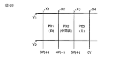
次に、上述した構成の液晶表示装置における駆動例について説明する。ここでは、説明を簡略にするため、図5に示すように、アクティブエリアDSPにおける1行の3画素(PX1、PX2、PX3)に着目し、5V駆動のノーマリーブラックモード(電位差が0Vのときに黒表示であって、電位差が5Vのときに白表示となるモード)の駆動例について説明する。 Next, a driving example in the liquid crystal display device having the above-described configuration will be described. Here, for the sake of simplicity, as shown in FIG. 5, focusing on one row of three pixels (PX1, PX2, PX3) in the active area DSP, a normally black mode of 5V drive (when the potential difference is 0V) A driving example of a mode in which black is displayed and white is displayed when the potential difference is 5 V will be described.
画素PX1は、信号線X1及びX2の間に配置され、その第1電極が信号線X1に接続されるとともにその第2電極が信号線X2に接続されている。画素PX2は、信号線X2及びX3の間に配置され、その第1電極が信号線X2に接続されるとともにその第2電極が信号線X3に接続されている。画素PX3は、信号線X3及びX4の間に配置され、その第1電極が信号線X3に接続されるとともにその第2電極が信号線X4に接続されている。 The pixel PX1 is disposed between the signal lines X1 and X2, and has a first electrode connected to the signal line X1 and a second electrode connected to the signal line X2. The pixel PX2 is disposed between the signal lines X2 and X3, and has a first electrode connected to the signal line X2 and a second electrode connected to the signal line X3. The pixel PX3 is disposed between the signal lines X3 and X4, and the first electrode is connected to the signal line X3 and the second electrode is connected to the signal line X4.
これらの3画素は、走査線Y1にそれぞれスイッチング素子を介して接続されており、走査線Y1にオン信号が供給された際に、各信号線を介して第1電極E1と第2電極E2との間に画素電位の書込が可能となるとともに、走査線Y1にオフ信号が供給されている期間内においては書き込まれた画素電位を保持している。例えば、画素PX2に着目すれば、走査線Y1がオフしている期間内は、画素PX2と信号線X3とのカップリングにより、他方の信号線の電位が変動しても、画素PX2の画素電位は保持される。 These three pixels are connected to the scanning line Y1 through switching elements, respectively, and when an ON signal is supplied to the scanning line Y1, the first electrode E1 and the second electrode E2 are connected through the signal lines. During this period, the pixel potential can be written, and the written pixel potential is held during the period in which the OFF signal is supplied to the scanning line Y1. For example, when focusing on the pixel PX2, even if the potential of the other signal line varies due to coupling between the pixel PX2 and the signal line X3 during the period when the scanning line Y1 is off, the pixel potential of the pixel PX2 Is retained.
そして、上述のような画素電位の書込に際しては、いずれの画素においても、一方の信号線の電位は、他方の信号線の電位を基準とした画素電位に設定されている。 When writing the pixel potential as described above, in any pixel, the potential of one signal line is set to a pixel potential based on the potential of the other signal line.
例えば、図6Aに示すように、画素PX3については、信号線X4の電位を基準電位、例えば0Vとし、信号線X3の電位を5Vとすることにより、白表示となる。また、画素PX3に隣接する画素PX2については、信号線X3の電位を基準電位(5V)とし、信号線X2の電位を10Vまたは0Vとすることにより、同じく白表示となる。このような手法によって各信号線の電位を設定することにより、所望の画面表示が可能となる。 For example, as shown in FIG. 6A, for the pixel PX3, when the potential of the signal line X4 is set to a reference potential, for example, 0 V, and the potential of the signal line X3 is set to 5 V, white display is performed. For the pixel PX2 adjacent to the pixel PX3, the potential of the signal line X3 is set to the reference potential (5V), and the potential of the signal line X2 is set to 10V or 0V, so that white display is also performed. By setting the potential of each signal line by such a method, a desired screen display can be performed.
なお、図6Aに示したように、画素PX3における画素電位の極性(正)に対して、これに隣接する画素PX2における画素電位の極性は、10Vを選択したときのように(正)であっても良いが、0Vを選択したときのように(負)であっても良い。一般的には、隣接する画素の画素電位の極性を反転させるVライン反転駆動やドット反転駆動(HV反転駆動)などの駆動手法を適用することで、最大信号振幅を低減できる。 As shown in FIG. 6A, the polarity of the pixel potential in the pixel PX3 (positive) is the same as the polarity of the pixel potential in the adjacent pixel PX2 (positive) as when 10V is selected. However, it may be (negative) as when 0V is selected. Generally, the maximum signal amplitude can be reduced by applying a driving method such as V-line inversion driving or dot inversion driving (HV inversion driving) that inverts the polarity of the pixel potential of adjacent pixels.
また、画素電位の極性は、規則的に反転させなくても良い。 Further, the polarity of the pixel potential may not be regularly reversed.
例えば、図6Bに示すように、画素PX3については、信号線X4の電位を基準電位(0V)とし、正極性を選択して、信号線X3の電位を5Vとすることにより、白表示となる。画素PX3に隣接する画素PX2については、1V相当の中間調を表示しようとする場合、信号線X3の電位を基準電位(5V)とし、負極性を選択して、信号線X2の電位を4Vとする。そして、画素PX2に隣接する画素PX1について、5V相当の白を表示しようとする場合、信号線X2の電位を基準電位(4V)とし、正極性を選択すると、信号線X1の電位は9Vとなる。このため、最大信号振幅は増大する傾向となる。 For example, as shown in FIG. 6B, for the pixel PX3, white potential is displayed by setting the potential of the signal line X4 to the reference potential (0V), selecting the positive polarity, and setting the potential of the signal line X3 to 5V. . For the pixel PX2 adjacent to the pixel PX3, when displaying a halftone equivalent to 1V, the potential of the signal line X3 is set to the reference potential (5V), the negative polarity is selected, and the potential of the signal line X2 is set to 4V. To do. Then, when displaying white equivalent to 5V for the pixel PX1 adjacent to the pixel PX2, if the potential of the signal line X2 is set to the reference potential (4V) and the positive polarity is selected, the potential of the signal line X1 becomes 9V. . For this reason, the maximum signal amplitude tends to increase.
そこで、図6Cに示すように、画素電位の極性に規則性を持たせず、画素PX1について、5V相当の白を表示しようとする場合には、信号線X2の電位を基準電位(4V)とし、負極性を選択することにより、信号線X1の電位は−1Vとなる。このような駆動手法により、最大信号振幅の増大を抑制することが可能となる。 Accordingly, as shown in FIG. 6C, when the pixel PX1 does not have regularity and the pixel PX1 is intended to display white corresponding to 5V, the potential of the signal line X2 is set to the reference potential (4V). By selecting the negative polarity, the potential of the signal line X1 becomes −1V. By such a driving method, an increase in the maximum signal amplitude can be suppressed.
つまり、信号線ドライバXDは、隣接する信号線の電位、隣接する画素の画素電位などに基づいて、出力可能な最大信号振幅を越えないように各信号線に供給する電圧を設定する。たとえば、信号線ドライバXDは、ある画素の画素電位を設定する際、基準電位に対して信号線に供給する電圧が上限のしきい値電圧VsigH(例えば5V)及び下限のしきい値電圧VsigL(例えば−5V)を超えないように画素電位の極性を選択する。あるいは、信号線ドライバXDは、中間駆動電圧Vsigc(例えば2.5V)に向かう側の極性を選択するようにしても良い。 That is, the signal line driver XD sets the voltage supplied to each signal line so as not to exceed the maximum signal amplitude that can be output, based on the potential of the adjacent signal line, the pixel potential of the adjacent pixel, and the like. For example, when the signal line driver XD sets the pixel potential of a certain pixel, the voltage supplied to the signal line with respect to the reference potential is the upper limit threshold voltage VsigH (for example, 5 V) and the lower limit threshold voltage VsigL ( For example, the polarity of the pixel potential is selected so as not to exceed −5V). Alternatively, the signal line driver XD may select the polarity toward the intermediate drive voltage Vsigc (for example, 2.5 V).
なお、この発明は、上記実施形態そのものに限定されるものではなく、その実施の段階ではその要旨を逸脱しない範囲で構成要素を変形して具体化できる。また、上記実施形態に開示されている複数の構成要素の適宜な組み合せにより種々の発明を形成できる。例えば、実施形態に示される全構成要素から幾つかの構成要素を削除してもよい。更に、異なる実施形態に亘る構成要素を適宜組み合せてもよい。 In addition, this invention is not limited to the said embodiment itself, In the stage of implementation, it can change and implement a component within the range which does not deviate from the summary. In addition, various inventions can be formed by appropriately combining a plurality of constituent elements disclosed in the embodiment. For example, some components may be deleted from all the components shown in the embodiment. Furthermore, you may combine suitably the component covering different embodiment.
LPN…液晶表示パネル
AR…アレイ基板
CT…対向基板
LQ…液晶層
DSP…アクティブエリア
Y…走査線
X…信号線
PX…画素
E1…第1電極(上部電極)
E2…第2電極(下部電極)
SL…スリット
XD…信号線ドライバ
Clc…液晶容量
Cs…補助容量
LPN ... Liquid crystal display panel AR ... Array substrate CT ... Counter substrate LQ ... Liquid crystal layer DSP ... Active area Y ... Scanning line X ... Signal line PX ... Pixel E1 ... First electrode (upper electrode)
E2 ... Second electrode (lower electrode)
SL ... Slit XD ... Signal line driver Clc ... Liquid crystal capacitance Cs ... Auxiliary capacitance
Claims (4)
マトリクス状の画素の行方向に延在する走査線と、
前記画素の列方向に延在する信号線と、
各画素において、隣接する信号線間に形成された蓄積容量素子と、
各画素に配置されたスイッチング素子と、
を備え、行方向に隣接する一対の信号線間の画素は、前記スイッチング素子を介して一方の信号線に接続された前記第1電極と、他方の信号線に接続された前記第2電極と、を有することにより、隣接する一対の信号線間に前記蓄積容量素子を形成したことを特徴とする液晶表示装置。 A lateral electric field mode liquid crystal display device having a configuration in which a liquid crystal layer is held between a pair of substrates, and one substrate includes a pair of first and second electrodes facing each other with an interlayer insulating film therebetween.
A scanning line extending in the row direction of the matrix-shaped pixels;
A signal line extending in the column direction of the pixels;
In each pixel, a storage capacitor element formed between adjacent signal lines;
A switching element disposed in each pixel;
A pixel between a pair of signal lines adjacent in the row direction includes: the first electrode connected to one signal line via the switching element; and the second electrode connected to the other signal line. , So that the storage capacitor element is formed between a pair of adjacent signal lines.
Priority Applications (2)
| Application Number | Priority Date | Filing Date | Title |
|---|---|---|---|
| JP2007269433A JP4662494B2 (en) | 2007-10-16 | 2007-10-16 | Liquid crystal display device |
| US12/236,169 US8542327B2 (en) | 2007-10-16 | 2008-09-23 | Liquid crystal display device |
Applications Claiming Priority (1)
| Application Number | Priority Date | Filing Date | Title |
|---|---|---|---|
| JP2007269433A JP4662494B2 (en) | 2007-10-16 | 2007-10-16 | Liquid crystal display device |
Publications (2)
| Publication Number | Publication Date |
|---|---|
| JP2009098374A JP2009098374A (en) | 2009-05-07 |
| JP4662494B2 true JP4662494B2 (en) | 2011-03-30 |
Family
ID=40533836
Family Applications (1)
| Application Number | Title | Priority Date | Filing Date |
|---|---|---|---|
| JP2007269433A Active JP4662494B2 (en) | 2007-10-16 | 2007-10-16 | Liquid crystal display device |
Country Status (2)
| Country | Link |
|---|---|
| US (1) | US8542327B2 (en) |
| JP (1) | JP4662494B2 (en) |
Families Citing this family (4)
| Publication number | Priority date | Publication date | Assignee | Title |
|---|---|---|---|---|
| JP4386102B2 (en) * | 2007-06-28 | 2009-12-16 | エプソンイメージングデバイス株式会社 | Horizontal electric field LCD panel |
| JP5707183B2 (en) | 2011-03-10 | 2015-04-22 | 株式会社ジャパンディスプレイ | Liquid crystal display |
| JP5520897B2 (en) | 2011-08-11 | 2014-06-11 | 株式会社ジャパンディスプレイ | Liquid crystal display |
| CN104102402B (en) * | 2014-06-25 | 2017-01-25 | 京东方科技集团股份有限公司 | Touch substrate and display device |
Citations (13)
| Publication number | Priority date | Publication date | Assignee | Title |
|---|---|---|---|---|
| JPH07128683A (en) * | 1993-11-04 | 1995-05-19 | Matsushita Electric Ind Co Ltd | Thin film transistor integrated device |
| JP2000047250A (en) * | 1998-07-24 | 2000-02-18 | Nec Corp | Liquid crystal display panel |
| JP2000056320A (en) * | 1998-08-05 | 2000-02-25 | Matsushita Electric Ind Co Ltd | Active matrix type liquid crystal display device |
| JP2000081637A (en) * | 1998-09-03 | 2000-03-21 | Nec Corp | Liquid crystal display device |
| JP2002287712A (en) * | 2001-03-28 | 2002-10-04 | Matsushita Electric Ind Co Ltd | Liquid crystal panel and method of manufacturing the same |
| JP2003015155A (en) * | 2001-06-28 | 2003-01-15 | Hitachi Ltd | Liquid crystal display device |
| JP2005077424A (en) * | 2003-08-29 | 2005-03-24 | Hitachi Displays Ltd | Liquid crystal display device |
| WO2005059637A1 (en) * | 2003-12-18 | 2005-06-30 | Sharp Kabushiki Kaisha | Display device |
| JP2005300780A (en) * | 2004-04-08 | 2005-10-27 | Sharp Corp | Display device |
| JP2005300779A (en) * | 2004-04-08 | 2005-10-27 | Sharp Corp | Display device |
| JP2006189758A (en) * | 2004-12-31 | 2006-07-20 | Lg Philips Lcd Co Ltd | Liquid crystal display device |
| JP2006235449A (en) * | 2005-02-28 | 2006-09-07 | Sanyo Epson Imaging Devices Corp | Electrooptic apparatus, driving method and electronic equipment |
| JP2006292854A (en) * | 2005-04-07 | 2006-10-26 | Sanyo Epson Imaging Devices Corp | Electrooptical device, method for driving the same, and electronic appliance |
Family Cites Families (9)
| Publication number | Priority date | Publication date | Assignee | Title |
|---|---|---|---|---|
| WO2004099868A1 (en) * | 1995-04-07 | 2004-11-18 | Shinya Kondoh | Antiferroelectric liquid crystal panel and method of its driving |
| JP2001174784A (en) | 1999-12-16 | 2001-06-29 | Hitachi Ltd | Liquid crystal display device |
| KR100653474B1 (en) | 2003-09-26 | 2006-12-04 | 비오이 하이디스 테크놀로지 주식회사 | fringe field switching liquid crystal display |
| US7171083B2 (en) * | 2004-02-04 | 2007-01-30 | Fujitsu Limited | One-by-N optical switch |
| JP4627148B2 (en) * | 2004-04-09 | 2011-02-09 | 株式会社 日立ディスプレイズ | Display device |
| JP4753561B2 (en) * | 2004-09-30 | 2011-08-24 | 日本碍子株式会社 | Electron emission device |
| JP2006139295A (en) | 2005-12-12 | 2006-06-01 | Hitachi Ltd | Liquid crystal display |
| KR101297804B1 (en) * | 2006-07-25 | 2013-08-20 | 삼성디스플레이 주식회사 | Array substrate and display panel having the same |
| JP2008096840A (en) * | 2006-10-13 | 2008-04-24 | Epson Imaging Devices Corp | Liquid crystal display |
-
2007
- 2007-10-16 JP JP2007269433A patent/JP4662494B2/en active Active
-
2008
- 2008-09-23 US US12/236,169 patent/US8542327B2/en active Active
Patent Citations (13)
| Publication number | Priority date | Publication date | Assignee | Title |
|---|---|---|---|---|
| JPH07128683A (en) * | 1993-11-04 | 1995-05-19 | Matsushita Electric Ind Co Ltd | Thin film transistor integrated device |
| JP2000047250A (en) * | 1998-07-24 | 2000-02-18 | Nec Corp | Liquid crystal display panel |
| JP2000056320A (en) * | 1998-08-05 | 2000-02-25 | Matsushita Electric Ind Co Ltd | Active matrix type liquid crystal display device |
| JP2000081637A (en) * | 1998-09-03 | 2000-03-21 | Nec Corp | Liquid crystal display device |
| JP2002287712A (en) * | 2001-03-28 | 2002-10-04 | Matsushita Electric Ind Co Ltd | Liquid crystal panel and method of manufacturing the same |
| JP2003015155A (en) * | 2001-06-28 | 2003-01-15 | Hitachi Ltd | Liquid crystal display device |
| JP2005077424A (en) * | 2003-08-29 | 2005-03-24 | Hitachi Displays Ltd | Liquid crystal display device |
| WO2005059637A1 (en) * | 2003-12-18 | 2005-06-30 | Sharp Kabushiki Kaisha | Display device |
| JP2005300780A (en) * | 2004-04-08 | 2005-10-27 | Sharp Corp | Display device |
| JP2005300779A (en) * | 2004-04-08 | 2005-10-27 | Sharp Corp | Display device |
| JP2006189758A (en) * | 2004-12-31 | 2006-07-20 | Lg Philips Lcd Co Ltd | Liquid crystal display device |
| JP2006235449A (en) * | 2005-02-28 | 2006-09-07 | Sanyo Epson Imaging Devices Corp | Electrooptic apparatus, driving method and electronic equipment |
| JP2006292854A (en) * | 2005-04-07 | 2006-10-26 | Sanyo Epson Imaging Devices Corp | Electrooptical device, method for driving the same, and electronic appliance |
Also Published As
| Publication number | Publication date |
|---|---|
| JP2009098374A (en) | 2009-05-07 |
| US20090096946A1 (en) | 2009-04-16 |
| US8542327B2 (en) | 2013-09-24 |
Similar Documents
| Publication | Publication Date | Title |
|---|---|---|
| JP4693131B2 (en) | Liquid crystal display | |
| JP5172508B2 (en) | Liquid crystal display | |
| TWI391761B (en) | Liquid crystal display device | |
| JP4911793B2 (en) | Liquid crystal display | |
| JP5380416B2 (en) | Liquid crystal display | |
| JP2005003802A (en) | Liquid crystal display device | |
| JP2009229599A (en) | Liquid crystal display | |
| JP2012173469A (en) | Liquid crystal display device and driving method for the same | |
| JP5100822B2 (en) | Liquid crystal display | |
| JP2013007956A (en) | Liquid crystal display device | |
| US8179512B2 (en) | Liquid crystal display device having particular pixel structure to decrease parasitic capacitance | |
| JP4662494B2 (en) | Liquid crystal display device | |
| JP5177887B2 (en) | Liquid crystal display | |
| JP4373999B2 (en) | Liquid crystal display | |
| JP2010066396A (en) | Liquid crystal display device | |
| JP5299083B2 (en) | Liquid crystal display | |
| JP5299872B2 (en) | Liquid crystal display | |
| JP2009098375A (en) | Liquid crystal display | |
| JP2009186514A (en) | Liquid crystal display device | |
| JP5450741B2 (en) | Liquid crystal display | |
| JP2010008919A (en) | Liquid crystal display device | |
| JP2009025638A (en) | Liquid crystal display device | |
| JP2009093022A (en) | Liquid crystal display device | |
| JP5299063B2 (en) | Liquid crystal display | |
| JP2007163590A (en) | Liquid crystal display device |
Legal Events
| Date | Code | Title | Description |
|---|---|---|---|
| A621 | Written request for application examination |
Free format text: JAPANESE INTERMEDIATE CODE: A621 Effective date: 20090612 |
|
| A977 | Report on retrieval |
Free format text: JAPANESE INTERMEDIATE CODE: A971007 Effective date: 20091130 |
|
| A131 | Notification of reasons for refusal |
Free format text: JAPANESE INTERMEDIATE CODE: A131 Effective date: 20091208 |
|
| A521 | Request for written amendment filed |
Free format text: JAPANESE INTERMEDIATE CODE: A523 Effective date: 20100203 |
|
| A131 | Notification of reasons for refusal |
Free format text: JAPANESE INTERMEDIATE CODE: A131 Effective date: 20100706 |
|
| A521 | Request for written amendment filed |
Free format text: JAPANESE INTERMEDIATE CODE: A523 Effective date: 20100823 |
|
| TRDD | Decision of grant or rejection written | ||
| A01 | Written decision to grant a patent or to grant a registration (utility model) |
Free format text: JAPANESE INTERMEDIATE CODE: A01 Effective date: 20101207 |
|
| A01 | Written decision to grant a patent or to grant a registration (utility model) |
Free format text: JAPANESE INTERMEDIATE CODE: A01 |
|
| A61 | First payment of annual fees (during grant procedure) |
Free format text: JAPANESE INTERMEDIATE CODE: A61 Effective date: 20101228 |
|
| R150 | Certificate of patent or registration of utility model |
Ref document number: 4662494 Country of ref document: JP Free format text: JAPANESE INTERMEDIATE CODE: R150 Free format text: JAPANESE INTERMEDIATE CODE: R150 |
|
| FPAY | Renewal fee payment (event date is renewal date of database) |
Free format text: PAYMENT UNTIL: 20140114 Year of fee payment: 3 |
|
| S533 | Written request for registration of change of name |
Free format text: JAPANESE INTERMEDIATE CODE: R313533 |
|
| FPAY | Renewal fee payment (event date is renewal date of database) |
Free format text: PAYMENT UNTIL: 20140114 Year of fee payment: 3 |
|
| R350 | Written notification of registration of transfer |
Free format text: JAPANESE INTERMEDIATE CODE: R350 |
|
| R250 | Receipt of annual fees |
Free format text: JAPANESE INTERMEDIATE CODE: R250 |
|
| R250 | Receipt of annual fees |
Free format text: JAPANESE INTERMEDIATE CODE: R250 |
|
| R250 | Receipt of annual fees |
Free format text: JAPANESE INTERMEDIATE CODE: R250 |
|
| R250 | Receipt of annual fees |
Free format text: JAPANESE INTERMEDIATE CODE: R250 |
|
| R250 | Receipt of annual fees |
Free format text: JAPANESE INTERMEDIATE CODE: R250 |
|
| R250 | Receipt of annual fees |
Free format text: JAPANESE INTERMEDIATE CODE: R250 |
|
| R250 | Receipt of annual fees |
Free format text: JAPANESE INTERMEDIATE CODE: R250 |
|
| R250 | Receipt of annual fees |
Free format text: JAPANESE INTERMEDIATE CODE: R250 |
|
| S111 | Request for change of ownership or part of ownership |
Free format text: JAPANESE INTERMEDIATE CODE: R313111 |
|
| R350 | Written notification of registration of transfer |
Free format text: JAPANESE INTERMEDIATE CODE: R350 |
|
| R250 | Receipt of annual fees |
Free format text: JAPANESE INTERMEDIATE CODE: R250 |
|
| R250 | Receipt of annual fees |
Free format text: JAPANESE INTERMEDIATE CODE: R250 |
|
| R250 | Receipt of annual fees |
Free format text: JAPANESE INTERMEDIATE CODE: R250 |