JP4649727B2 - Method for manufacturing thin film member - Google Patents
Method for manufacturing thin film member Download PDFInfo
- Publication number
- JP4649727B2 JP4649727B2 JP2000344125A JP2000344125A JP4649727B2 JP 4649727 B2 JP4649727 B2 JP 4649727B2 JP 2000344125 A JP2000344125 A JP 2000344125A JP 2000344125 A JP2000344125 A JP 2000344125A JP 4649727 B2 JP4649727 B2 JP 4649727B2
- Authority
- JP
- Japan
- Prior art keywords
- thin film
- displacement
- flat plate
- radiation
- film member
- Prior art date
- Legal status (The legal status is an assumption and is not a legal conclusion. Google has not performed a legal analysis and makes no representation as to the accuracy of the status listed.)
- Expired - Fee Related
Links
Images

Landscapes
- Radiation Pyrometers (AREA)
- Solid State Image Pick-Up Elements (AREA)
- Photometry And Measurement Of Optical Pulse Characteristics (AREA)
Description
【0001】
【発明の属する技術分野】
本発明は、マイクロマシンや微少な素子を有する各種のデバイスなどにおいて用いられる薄膜部材、及びこれを用いた放射検出装置に関するものである。
【0002】
【従来の技術】
従来から、マイクロマシンや、微少な素子を有する各種のデバイスなどにおいては、空中に位置するように支持された平板状部を備えた薄膜部材が用いられている。この薄膜部材は、一般的に、半導体製造工程を用いて作製されている。
【0003】
例えば、特開2000−9542号に開示された光読み出し型の熱型放射検出装置は、基体と、該基体に支持され、放射を吸収する放射吸収部にて発生した熱に応じて前記基体に対して変位する変位部と、該変位部に対して固定された読み出し光反射板とを備えており、この反射板として前記薄膜部材が用いられている。
【0004】
前述したような従来の薄膜部材では、前記平板状部は、単に、所望の平面形状を有する1層以上の膜からなる平面部のみで構成されていた。
【0005】
【発明が解決しようとする課題】
前記従来の薄膜部材では、平板状部が単に所望の平面形状を有する1層以上の膜からなる平面部のみで構成されていたので、所望の機械的強度を確保するためには、膜厚を厚くしなければならなかった。特に、平板状部の面積が比較的大きい場合には、膜厚をかなり厚くしなければならなかった。このため、従来の薄膜部材では、その用途に応じて種々の不都合が生じていた。
【0006】
本発明は、このような事情に鑑みてなされたもので、所望の機械的強度を確保しつつ膜厚を薄くすることができる薄膜部材を提供することを目的とする。
【0007】
また、本発明は、所望の機械的強度を確保しつつ膜厚を薄くすることができる薄膜部材を用いることによって、感度等の特性の向上を図ることができる放射検出装置を提供することを目的とする。
【0008】
【課題を解決するための手段】
前記課題を解決するため、本発明の第1の態様による薄膜部材は、空中に位置するように支持された平板状部を備えた薄膜部材であって、前記平板状部は、1層又は複数層の膜からなる平面部と、該平面部に混在するように形成され前記平面部の表面側又は裏面側に突出した凸条部とを有するものである。ここで、「混在する」とは、凸条部が平面部に混じって存在することを意味し、凸条部が平面部に必ずしも複雑に混じり込む必要はなく、凸条部が平面部に単純な形で混じっていてもよい。この第1の態様による薄膜部材は、通常、半導体製造工程を用いて作製される。
【0009】
この第1の態様によれば、平板状部が平面部のみならずこれに混在された凸条部を有しているので、平面部が凸条部により補強される。したがって、平板状部の所望の機械的強度を確保しつつ、平板状部の膜厚を薄くすることができる。
【0010】
また、平面部を複数層の膜で構成した場合、各層の膜の膨張係数の差によって平面部が温度変化により変位しようとしても、その変位が凸条部によって阻止され、平面部の平坦性が維持されることとなる。
【0011】
本発明の第2の態様による薄膜部材は、前記第1の態様において、前記凸条部は、前記平面部を実質的に複数の領域に区分するように形成されたものである。
この第2の態様のように凸条部を形成すると、凸条部により実質的に区分された平面部の個々の領域の面積が小さくなるので、平板状部の機械的強度を向上させる上で好ましい。
【0012】
本発明の第3の態様による薄膜部材は、前記第1又は第2の態様において、前記凸条部は、前記平面部を、前記平板状部の周辺部分から隔てられた1つ以上の領域、及び、当該各領域の周辺部分の一部が前記平板状部の周辺部分の一部となる複数の領域に、実質的に区分するように、形成されたものである。
【0013】
この第3の態様のように、平面部を中央寄りの1つ以上の領域及び周辺寄りの複数の領域に実質的に区分するように、凸条部を形成すると、凸条部により実質的に区分された平面部の個々の領域の面積が小さくなることと相俟って、後述する第4の態様のような凸条部の配置を実現し易くなるため、平板状部の機械的強度を向上させる上で好ましい。
【0014】
本発明の第4の態様による薄膜部材は、前記第1乃至第3のいずれかの態様において、前記凸条部は、前記平板状部の周辺部分の任意の2点を結ぶ各仮想直線について、当該仮想直線の全体に渡っては前記凸条部が位置することがないように、形成されたものである。
【0015】
本発明者の実験の結果、平板状部の周辺部分の2点(例えば、ある点とこの点に対向する点)を結ぶ仮想直線の全体に渡って凸条部が位置するように形成すると、この直線に沿って平板状部が曲がり易くなる一方、前記第4の態様のように凸条部を形成すれば、そのような曲がりが生じ難くなり、平板状部の機械的強度を向上させる上で好ましいことが判明した。
【0016】
本発明の第5の態様による薄膜部材は、前記第1乃至第4のいずれかの態様において、前記凸条部は、曲線状に形成された部分を含むものである。
【0017】
この第5の態様のように、凸条部が曲線状に形成された部分を含むと、前記第4の態様のような凸条部の配置を実現し易くなるため、平板状部の機械的強度を向上させる上で好ましい。
【0018】
本発明の第6の態様による薄膜部材は、前記第1乃至第5のいずれかの態様において、前記凸条部の少なくとも一部の断面形状が、突出側と反対の側に開口する略コ字状であるか、あるいは、略中実形状であるものである。
【0019】
この第6の態様は凸条部の断面形状の例を挙げたものであるが、前記第1乃至第5の態様ではこの例に限定されるものではない。
【0020】
本発明の第7の態様による薄膜部材は、前記第1乃至第6のいずれかの態様において、前記凸条部は、前記平面部を構成する少なくとも1層の膜からそれと同じ材料で連続して一体に形成されたものである。
【0021】
この第7の態様によれば、平面部の少なくとも1層の膜を形成する際に凸条部を同時に形成することができるので、製造が容易となる。もっとも、前記第1乃至第6の態様では、凸条部は、例えば、平面部と別の材料で形成してもよい。
【0022】
本発明の第8の態様による薄膜部材は、前記第1乃至第7のいずれかの態様において、前記平面部の各領域の周辺部分のうち前記平板状部の周辺部分となる部分の少なくとも一部に渡って、当該平面部から立ち上がるかあるいは立ち下がる立ち上がり部又は立ち下がり部が形成されたものである。
【0023】
この第8の態様によれば、平板状部は立ち上がり部又は立ち下がり部によっても補強される。したがって、平板状部の所望の機械的強度を確保しつつ、平板状部の膜厚を一層薄くすることができる。
【0024】
本発明の第9の態様による放射検出装置は、基体と、該基体に支持され、放射を吸収する放射吸収部にて発生した熱に応じて前記基体に対して変位する変位部と、該変位部に対して固定された変位読み出し部材であって、前記変位部に生じた変位に応じた所定の変化を得るために用いられる変位読み出し部材とを備えた放射検出装置において、前記変位読み出し部材が前記第1乃至第8のいずれかの態様による薄膜部材で構成されたものである。
【0025】
この第9の態様によれば、変位読み出し部材が前記第1乃至第8のいずれかの態様による薄膜部材で構成されているので、変位読み出し部材の所望の機械的強度を確保しつつ、変位読み出し部材の膜厚を薄くすることができる。このため、変位読み出し部材の軽量化を図ることができるので、変位部の機械的強度を低下させることができ、変位部の膜厚を薄くすることができる。変位部は、通常、異なる膨張係数を有する異なる物質の互いに重なった少なくとも2つの層を有する構造を持つが、変位部の膜厚が薄いほど温度変化に対する変位量が大きくなって感度が高くなる。したがって、前記第9の態様によれば、変位部の感度を高めることができ、ひいては、放射検出の感度を高めることができる。また、変位部に対して固定された変位読み出し部材の膜厚を薄くすることができるので、これら全体としての熱容量が少なくなる。このため、熱に対する応答性が高まり、ひいては検出すべき放射の変化に対する応答性が高まる。
【0026】
前記第9の態様において、前記変位読み出し部材は、例えば、受光した読み出し光を反射する反射板であってもよいし、電極であってもよい。前者は、前記第9の態様を、入射放射量を読み出し光の変化として読み出すいわば光読み出し型の放射検出装置に適用した例である。後者は、前記第9の態様を、入射放射量を静電容量の変化として読み出す静電容量型の放射検出装置等に適用した例である。もっとも、前記第9の態様は、これらのタイプの放射検出装置に限定されるものではない。これらの点は、後述する第10の態様についても同様である。なお、前記第1乃至第8の態様による薄膜部材は、例えば、ボロメータ素子の受光部に適用することもできる。
【0027】
前記第9の態様による放射検出装置において、前記変位部及び前記変位読み出し部材を1個の素子として当該素子を複数個設け、当該素子を1次元状又は2次元状に配列してもよい。この場合、放射の像を映像化することが可能となるが、前記第9の態様では、変位部及び変位読み出し部材の対を1個のみ有していてもよい。これらの点は、後述する第10の態様についても同様である。前記第9の態様では、読み出し部材の形状が安定化することから、前記素子を複数個設ける場合には、各素子間での読み出し部材の形状のばらつきが小さくなるので、各素子間での変位読み出し特性のばらつきが小さくなり、ひいては、各素子間での放射検出特性のばらつきが小さくなるという効果も得られる。
【0028】
本発明の第10の態様による放射検出装置は、基体と、該基体に支持され、放射を吸収する放射吸収部にて発生した熱に応じて前記基体に対して変位する変位部とを備えた放射検出装置において、前記放射吸収部が入射した放射の一部を反射する特性を有し、nを奇数、前記放射の所望の波長域の中心波長をλ0として、前記放射吸収部から実質的にnλ0/4の間隔をあけて配置され前記放射を略々全反射する放射反射部を備え、前記放射吸収部及び前記放射反射部の少なくとも一方が前記第1乃至第8のいずれかの態様による薄膜部材で構成されたものである。
【0029】
この第10の態様によれば、放射吸収部に放射反射部と反対側から放射が入射すると、入射した放射は放射吸収部で一部吸収され、残りは放射反射部で反射され放射吸収部で反射し再度放射反射部に入射する。このため、放射吸収部と放射反射部との間で干渉現象が起こり、両者の間隔が入射放射の所望の波長域の中心波長の1/4の略奇数倍とされているので、放射吸収部での放射吸収がほぼ最大となり、放射吸収部における放射の吸収率が高まる。したがって、放射吸収部の厚みを薄くしてその熱容量を小さくしても、放射の吸収率を高めることができる。その結果、検出感度及び検出応答性の両方を高めることができる。なお、前記放射吸収部の反射率を約33%(約1/3)にすると、放射吸収部における放射の吸収率が一層高まるので、好ましい。
【0030】
そして、前記第10の態様では、放射吸収部及び放射反射部の少なくとも一方が前記第1乃至第8のいずれかの態様による薄膜部材で構成されているので、放射吸収部や放射反射部の所望の機械的強度を確保しつつ、放射吸収部や放射反射部の膜厚を薄くすることができる。このため、放射吸収部や放射反射部の軽量化を図ることができるので、放射吸収部や放射反射部を直接的又は間接的に変位部により支持されるように設けた場合であっても、変位部の機械的強度を低下させることができ、変位部の膜厚を薄くすることができる。したがって、前記第10の態様によれば、前記第9の態様と同様に、変位部の感度を高めることができ、ひいては、放射検出の感度を高めることができる。また、前記第10の態様によれば、放射吸収部や放射反射部の膜厚を薄くすることができるので、放射吸収部や放射反射部を変位部に対して直接的又は間接的に固定した場合、これら全体としての熱容量が少なくなる。このため、熱に対する応答性が高まり、ひいては検出すべき放射の変化に対する応答性が高まる。なお、前記第10の態様において、前記第9の態様の事項を具備していてもよいことは、言うまでもない。
【0031】
なお、前記第9及び第10の態様は、前記第1乃至第8の態様による薄膜部材を放射検出装置に用いた例であったが、前記第1乃至第8の態様による薄膜部材は、他の種々のデバイスやマイクロマシン等において用いることもできる。
【0032】
【発明の実施の形態】
以下の説明では、放射を赤外線とし読み出し光を可視光とした例について説明するが、本発明では、放射を赤外線以外のX線や紫外線やその他の種々の放射としてもよいし、また、読み出し光を可視光以外の他の光としてもよい。
【0033】
[第1の実施の形態]
【0034】
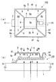
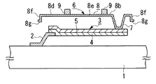
図1は本発明の第1の実施の形態による光読み出し型の放射検出装置100の単位画素(単位素子)を示す図であり、図1(a)はその概略平面図、図1(b)は図1(a)中のX1−X2線に沿った概略断面図である。
【0035】
この放射検出装置100は、基体としての赤外線iを透過させるSi基板等の基板1と、脚部2を介して基板1に支持され熱に応じて基板1に対して変位する変位部3と、変位部3に生じた変位に応じた所定の変化を得るために用いられる変位読み出し部材としての、受光した読み出し光jを反射する反射板6を備えている。
【0036】
変位部3は、互いに重なった2つの膜4,5を有している。変位部3は、その一端が脚部2を介して支持されることにより、カンチレバーを構成しており、基板1上に間隔をあけて浮いた状態に支持されている。膜4及び膜5は、互いに異なる膨張係数を有する異なる物質で構成されており、いわゆる熱バイモルフ構造(bi-material elementともいう。)を構成している。したがって、変位部3は、受けた熱に応じて、下側の膜4の膨張係数が上側の膜5の膨張係数より大きい場合には上方に、逆の場合には下方に湾曲して傾斜する。
【0037】
本実施の形態では、変位部3が赤外線iを吸収する赤外線吸収部を兼用している。したがって、変位部3は、赤外線iを受けると、自身が熱を発生し、この熱に応じて変位することとなる。もっとも、必ずしも変位部3が赤外線吸収部を兼用する必要はなく、例えば、膜4の下面に金黒等の赤外線吸収膜を形成しておいてもよい。
【0038】
反射板6は、その一部が反射板用接続部7を介して変位部3の先端部に対して固定されることにより、変位部3の上方に空間を隔てて配置され、単位画素領域のほぼ全体をカバーするように配置されている。これにより、反射板6は、空中に位置するように支持されている。反射板6は平面視で正方形状の平板状部からなる薄膜部材で構成され、この平板状部は、1層の膜(2層以上の膜でもよい)からなる平面部8と、平面部8に混在するように形成され平面部8の下面側(裏面側)に突出した凸条部9とから構成されている。すなわち、平面部8及び凸条部9の全体が、平板状部を構成している。平面部8が、平板状部の面積の大部分を占めており、読み出し光jを反射する反射面として実質的に有効な部分となっている。
【0039】
本実施の形態では、凸条部9は、図1(a)に示すように、平面部8を、平板状部の周辺部分から隔てられた1つの領域8e、及び、当該各領域8a〜8dの周辺部分の一部が平板状部の周辺部分の一部となる4つの領域8a〜8dの、合計5つの領域8a〜8eに、区分するように形成されている。そして、図1に示すように、平板状部の周辺部分の任意の2点を結ぶ各仮想直線について、当該仮想直線の全体に渡っては前記凸条部が位置することがないように、形成されている。また、凸条部9の断面形状は、図1(b)に示すように、凸条部9の突出側と反対の側(上側)に開口する略コ字状に構成されている。さらに、凸条部9は、平面部8を構成する膜からそれと同じ材料で連続して一体に形成されている。
【0040】
さらに、本実施の形態では、平面部8の各領域8a〜8eの周辺部分のうち平板状部の周辺部分となる部分(具体的には、図1において、領域8aの上辺部分、領域8bの右辺部分、領域8cの下辺部分、領域8dの左辺部分)の全体(その一部でもよい)に渡って、平面部8から立ち下がる立ち下がり部8fが形成されている。そして、立ち下がり部8fの下部から側方に外側にわずかに延びた水平部8gも、形成されている。水平部8gは、必ずしも必要ではなく、取り除いておいてもよい。また、立ち下がり部8fは、強度をより向上させるためには形成しておくことが好ましいが、本発明では必ずしも形成しておかなくてもよい。
【0041】
本実施の形態では、平面部8、凸条部9、立ち下がり部8f及び水平部8gは、反射板用接続部7と共に、Al膜等の1層の膜で一体に形成されている。なお、反射板用接続部7は、反射板6より熱伝導率の低い材料で構成してもよい。わずかながら読み出し光jの一部が反射板6に吸収されて反射板6の温度が上昇するが、接続部7を反射板6より熱伝導率の低い材料で構成しておけば、接続部7が断熱材として作用してその熱が変位部3に伝わり難くなり、赤外線検出のS/Nが高まるので、好ましい。
【0042】
図面には示していないが、変位部3、脚部2及び反射板6を単位素子(画素)として、この画素が基板1上に1次元状又は2次元状に配置されている。
【0043】
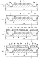
次に、本実施の形態による放射検出装置100の製造方法の一例について、図2を参照して説明する。図2は、この製造工程を模式的に示す概略断面図であり、図1(b)に対応している。
【0044】
まず、図2(a)に示すように、Si基板1上の全面に犠牲層としてのレジスト10を塗布し、脚部2に応じた開口10aをフォトリソグラフィーにより形成する。次に、脚部2となるべきSiO膜(例えば、厚さ5000オングストローム)をP−CVD法等によりデポした後、フォトエッチ法によりパターニングし、脚部2の形状とする(図2(a))。その後、変位部3の下側膜4となるべきSiN膜(例えば、厚さ2500オングストローム)をP−CVD法等によりデポした後、フォトエッチ法によりパターニングし、下側膜4の形状とする(図2(a))。さらに、変位部3の上側膜5となるべきAl膜(例えば、厚さ1500オングストローム)を蒸着法等によりデポした後、フォトエッチ法によりパターニングし、上側膜5の形状とする(図2(a))。
【0045】
次に、図2(a)に示す状態の基板上の全面に犠牲層としてのレジスト11を塗布し、反射板用接続部7に応じた開口11aをレジスト11にフォトリソグラフィーにより形成する(図2(b))。
【0046】
その後、図2(b)に示す状態の基板上の全面にスピンコート法等により犠牲層としてのポリイミド膜12を被着させ、反射板6の立ち下がり部8f及び水平部8gに応じた溝12a、反射板用接続部7に応じた開口12b並びに凸条部9に応じた溝12cを、ポリイミド膜12にフォトエッチ法により形成する(図2(c))。
【0047】
次いで、図2(c)に示す状態の基板上に、反射板6及び反射板用接続部7となるべきAl膜(例えば、厚さ2000オングストローム)を蒸着法等(例えば、抵抗加熱蒸着法、電子ビーム蒸着法、スパッタ法、MBE法など)により形成した後、フォトエッチ法によりパターニングし、反射板6の形状とする(図2(d))。このとき、Al膜のパターニングによって残す領域を、ポリイミド膜12と重なりかつポリイミド膜12の大きさよりも大きくすることによって、立ち下がり部8f及び水平部8gが形成されることとなる。また、このAl膜により、平面部8のみならず、凸条部9も同時に形成されることになる。なお、前記Al膜のパターニングの大きさを適宜変更することによって、水平部8gを形成しないようにすることも可能である。なお、反射板6及び反射板用接続部7となるべき薄膜の材質は、Alに代えて、例えば、Cu、Au、Pt、Pd、Ti、Ta、Cr、Sn、W又はMoなどを用いてもよい。
【0048】
最後に、図2(d)に示す状態の基板を、ダイシングなどによりチップ毎に分割し、レジスト10,11及びポリイミド膜12をアッシング法などにより除去する。これにより、図1に示す放射検出装置が完成する。
【0049】
本実施の形態によれば、反射板6を構成する平板状部が平面部8のみならずこれに混在された凸条部9を有しているので、平面部8が凸条部9により補強される。したがって、反射板6の所望の機械的強度を確保しつつ、反射板6の膜厚を薄くすることができている。そして、本実施の形態では、凸条部9が平面部8を複数の領域8a〜8eに区分するように形成されていることから、凸条部9により区分された平面部8の個々の領域8a〜8eの面積が小さくなるので、反射板6の機械的強度が更に向上している。また、本実施の形態では、凸条部9が平板状部の周辺部分の任意の2点を結ぶ各仮想直線について、当該仮想直線の全体に渡っては凸条部9が位置することがないように、形成されているので、反射板6が曲がり難くなり、反射板6の機械的強度が更に向上している。さらに、本実施の形態による放射検出装置では、反射板6は立ち下がり部8fによっても補強されるので、反射板6の機械的強度が更に向上している。
【0050】
このように、反射板6の所望の機械的強度を確保しつつ反射板6の膜厚(特に、平面部8の膜厚)を薄くすることができるので、反射板6の軽量化を図ることができる。このため、反射板6を支持している変位部3の機械的強度を低下させることができ、変位部3を構成する膜4,5の膜厚を薄くすることができる。変位部3の膜厚が薄くなるほど、温度の変化量に対する変位部3の変位量が増大し、変位部3の感度が高まる。したがって、本実施の形態によれば、変位部3の感度を高めることができ、赤外線検出の感度を高めることができる。
【0051】
また、本実施の形態によれば、変位部3に対して固定された反射板6の膜厚を薄くすることができるので、これら全体としての熱容量が少なくなる。このため、熱に対する応答性が高まり、ひいては赤外線の変化に対する応答性が高まる。
【0052】
さらに、本実施の形態によれば、反射板6を構成する平板状部が平面部8のみならずこれに混在された凸条部9を有しているので、反射板6の形状が安定化する。このため、各画素間での反射板6の形状のばらつきが小さくなるので、各画素間での変位読み出し特性のばらつきが小さくなり、ひいては、各画素間での赤外線検出特性のばらつきが小さくなるという効果も得られる。
【0053】
さらにまた、本実施の形態によれば、凸条部9は、平面部8を構成する膜からそれと同じ材料で連続して一体に形成されていることから、前述したように、平面部8及び凸条部9を同時に形成することができるので、製造が容易となる。
【0054】
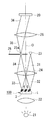
ここで、本実施の形態による放射検出装置100を用いた映像化装置の一例について、図3を参照して説明する。図3は、この映像化装置を示す概略構成図である。
【0055】
この映像化装置は、前述した放射検出装置100の他に、読み出し光学系と、撮像手段としての2次元CCD20と、観察対象(目標物体)としての熱源21からの赤外線iを集光して、放射検出装置100の赤外線吸収部としての変位部3が分布している面上に、熱源21の赤外線画像を結像させる赤外線用の結像レンズ22とから構成されている。
【0056】
この映像化装置では、前記読み出し光学系は、読み出し光を供給するための読み出し光供給手段としてのLD(レーザーダイオード)23と、LD23からの読み出し光を放射検出装置100の全ての画素の反射板6へ導く第1レンズ系24と、第1レンズ系24を通過した後に全ての画素の反射板6にて反射された読み出し光の光線束のうち所望の光線束のみを選択的に通過させる光線束制限部25と、第1レンズ系25と協働して各画素の反射板6と共役な位置を形成し且つ該共役な位置に光線束制限部25を通過した光線束を導く第2レンズ系26とから構成されている。前記共役な位置にはCCD20の受光面が配置されており、レンズ系24,26によって全ての画素の反射板6とCCD20の複数の受光素子とが光学的に共役な関係となっている。
【0057】
LD23は、第1レンズ系24の光軸Oに関して一方の側(図3中の右側)に配置されており、当該一方の側の領域を読み出し光が通過するように読み出し光を供給する。本例では、LD23が第1レンズ系24の第2レンズ系26側の焦点面付近に配置されて、第1レンズ系24を通過した読み出し光が略平行光束となって全ての画素の反射板6を照射するようになっている。CCD20上の光学像のコントラストを高めるため、LD23の前部に読み出し光絞りを設けてもよい。本例では、放射検出装置100は、その基板1の面(本例では、目標物体からの赤外線が入射しない場合の反射板6の面と平行)が光軸Oと直交するように配置されている。もっとも、このような配置に限定されるものではない。
【0058】
光線束制限部25は、前記所望の光線束のみを選択的に通過させる部位が第1レンズ系24の光軸Oに関して他方の側(図3中の左側)の領域に配置されるように構成されている。本例では、光線束制限部25は、開口25aを有する遮光板からなり、開口絞りとして構成されている。本例では、いずれの画素の赤外線吸収膜を兼ねる変位部3にも目標物体からの赤外線が入射していなくて全ての画素の反射板6の面が基板1の面と平行である場合に、全ての画素の反射板6で反射した光線束(各反射板6で反射した個別光線束の束)が第1レンズ系24によって集光する集光点の位置と開口25aの位置とがほぼ一致するように、光線束制限部25が配置されている。また、開口25aの大きさは、この光線束の前記集光点での断面の大きさとほぼ一致するように定められている。もっとも、このような配置や大きさに限定されるものではない。
【0059】
図3に示す映像化装置によれば、LD23から出射した読み出し光の光線束31は、第1レンズ系24に入射し、略平行化された光線束32となる。次にこの略平行化された光線束32は、放射検出装置100の全ての画素の反射板6に、基板1の法線に対してある角度をもって入射する。
【0060】
一方、結像レンズ22によって、熱源(目標物体)21からの赤外線が集光され、放射検出装置100の変位部3が分布している面上に、熱源21の赤外線画像が結像される。これにより、放射検出装置100の各画素の変位部3に熱源21からの赤外線が入射する。この入射赤外線は、各画素の反射板6の傾きに変換される。
【0061】
今、全ての画素の変位部3には熱源21からの赤外線が入射しておらず、全ての画素の反射板6が基板1と平行であるものとする。全ての画素の反射板6に入射した光線束32は、これらの反射板6にて反射されて光線束33となり、再び第1レンズ系24に今度はLD23の側とは反対の側から入射して集光光束34となり、この集光光束34の集光点の位置に配置された光線束制限部25の開口25aの部位に集光する。その結果、集光光束34は開口25aを透過して発散光束35となって第2レンズ系26に入射する。第2レンズ系26に入射した発散光束35は、第2レンズ系26により例えば略平行光束36となってCCD20の受光面に入射する。ここで、各画素の反射板6とCCD20の受光面とはレンズ系24,26によって共役な関係にあるので、CCD20の受光面上の対応する各部位にそれぞれ各反射板6の像が形成され、全体として、全ての画素の反射板6の分布像である光学像が形成される。
【0062】
今、ある画素の変位部3に熱源21からある量の赤外線が入射して、その入射量に応じた量だけ当該画素の反射板6が基板1の面に対して傾いたものとする。光線束32のうち当該反射板6に入射する個別光線束は、当該反射板6によってその傾き量だけ異なる方向に反射されるので、第1レンズ系24を通過した後、その傾き量に応じた量だけ前記集光点(すなわち、開口25a)の位置からずれた位置に集光し、その傾き量に応じた量だけ光線束制限部25により遮られることになる。したがって、CCD20上に形成された全体としての光学像のうち当該反射板6の像の光量は、当該反射板6の傾き量に応じた量だけ低下することになる。
【0063】
したがって、CCD20の受光面上に形成された読み出し光による光学像は、放射検出装置100に熱源21から入射した赤外線像を反映したものとなる。この光学像は、CCD20により撮像される。なお、CCD20を用いずに、接眼レンズ等を用いて前記光学像を肉眼で観察してもよい。
【0064】
なお、読み出し光学系の構成が前述した構成に限定されるものではないことは、言うまでもない。
【0065】
以上は映像化装置の例であったが、図3において、放射検出装置100として、単一の画素(素子)のみを有する放射検出装置を用い、2次元CCD20に代えて、単一の受光部のみを有する光検出器を用いれば、赤外線のいわゆるポイントセンサとしての検出装置を構成することができる。この点は、後述する各実施の形態についても同様である。
【0066】
[第2の実施の形態]
【0067】
図4は、本発明の第2の実施の形態による光読み出し型の放射検出装置の単位画素(単位素子)を示す概略断面図であり、図1(b)に対応している。図4において、図1中の要素と同一又は対応する要素には同一符号を付し、その重複する説明は省略する。
【0068】
本実施の形態が前記第1の実施の形態と異なる所は、反射板6の凹凸構成が逆になっている点のみである。すなわち、本実施の形態では、すなわち、反射板6において、凸条部9が平面部8の上面側(表面側)に突出し、立ち下がり部8fに代えて立ち上がり部8f’が形成されている点のみである。本実施の形態も前記第1の実施の形態と同様の製造方法によって製造することができることは、言うまでもない。
【0069】
本実施の形態によっても、前記第1の実施の形態と同様の利点が得られる。
【0070】
[第3の実施の形態]
【0071】
図5は、本発明の第3の実施の形態による光読み出し型の放射検出装置の単位画素(単位素子)を示す概略断面図であり、図1(b)に対応している。図5において、図1中の要素と同一又は対応する要素には同一符号を付し、その重複する説明は省略する。
【0072】
本実施の形態が前記第1の実施の形態と異なる所は、反射板6の凸条部9の断面形状が略中実形状とされている点のみである。本実施の形態も、前記第1の実施の形態と同様の製造方法によって製造することができる。この場合、図2(c)に示す工程において凸条部9に対応する溝12cの幅を狭めておけば、図2(d)に示す工程において、断面略中実形状の凸条部9が形成されることになる。
【0073】
本実施の形態によっても、前記第1の実施の形態と同様の利点が得られる。
【0074】
[第4の実施の形態]
【0075】
図6は、本発明の第4の実施の形態による光読み出し型の放射検出装置の単位画素(単位素子)を示す概略断面図であり、図1(b)に対応している。図6において、図1中の要素と同一又は対応する要素には同一符号を付し、その重複する説明は省略する。
【0076】
本実施の形態が前記第1の実施の形態と異なる所は、反射板6において、凸条部9が、平面部8を構成する膜とは別の材料で形成されている点である。本実施の形態も、前記第1の実施の形態と同様の製造方法によって製造することができる。この場合、図2(c)に示す工程において凸条部9に対応する溝12cは形成せず、図2(d)に示す工程の後に、凸条部9を構成することになる膜を形成し、その膜を凸条部9の形状にパターニングすればよい。
【0077】
本実施の形態によっても、前記第1の実施の形態と同様の利点が得られる。
【0078】
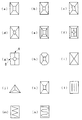
[凸条部のパターン例]
【0079】
前記第1乃至第5の実施の形態では、反射板6における平面視での凸条部9のパターンは、前述したように図1(a)に示す通りであった。このパターンを模式的に示したものが、図7(a)である。ただし、図7(a)では、平板状部の平面視での外形は長方形状となっている。図7(b)〜(n)は、平面視での凸条部9の他のパターンをそれぞれ模式的に示す図である。図7(a)〜(n)において、外形線以外の線は凸条部9を示し、線で囲まれた領域は平面部8の領域を示している。ただし、これらの図において、凸条部9の幅は省略している。
【0080】
前述した第1乃至第4の実施の形態において、反射部6における平面視での凸条部9のパターンを、図1(a)及び図7(b)に示すパターンの代わりに、例えば、図7(b)〜(n)に示すパターンとしてもよい。
【0081】
既に説明したように、図1(a)及び図7(b)に示すパターンでは、強度が大幅に向上する。このようなパターンの場合に強度が大幅に向上することは、本発明者の実験により判明した。
【0082】
図7(b)〜(d)に示すパターンは、凸条部9により区切られた平面部8の中央の領域の形状がそれぞれ円形、たなびいた旗のような形状、及び菱形となるように、図1(a)及び図7(a)に示すパターンを変更したものである。これらのパターンであっても、図1(a)及び図7(a)に示すパターンと同様に、強度が向上する。
【0083】
図7(e)(f)に示すパターンはそれぞれ、凸条部9により区切られた平板状部の領域のうち平板状部の周辺部分から隔てられた領域(中央寄りの領域)が5つとなるように、凸条部9が形成されたものである。これらのパターンであっても、図1(a)及び図7(a)に示すパターンと同様に、強度が向上する。
【0084】
図7(g)に示すパターンは、図7(b)において平板状部の対角線に沿ってX字状に配置された凸条部9の部分を、十字状に配置し直したものである。このパターンによっても凸条部9を形成しない場合に比べて強度が大幅に向上するが、図7(b)に示すパターンに比べると、例えば図7(g)中のA点とB点とを結ぶ直線に沿って比較的曲がり易いことから、やや強度が低下する。
【0085】
図7(h)に示すパターンは、図1(a)及び図7(a)に示すパターンと基本的に同じであるが、平板状部の形状が、図1(a)及び図7(a)の場合の平板状部の角部を面取りした形状となっている。この平板状部の外形や凸条部9のパターンであっても、図1(a)及び図7(a)に示す場合と同様に、強度が向上する。
【0086】
図7(i)に示すパターンでは、長方形状の平板状部の対角線に完全に沿うように、凸条部9が形成されている。このパターンによっても凸条部9を形成しない場合に比べて強度が大幅に向上するが、図7(a)〜(h)に示すパターンのように、平板状部の周辺部分の任意の2点を結ぶ各仮想直線について、当該仮想直線の全体に渡っては前記凸条部が位置することがないように、凸条部9が形成されている場合に比べると、図7(g)中の対角線に沿って比較的曲がり易いことから、やや強度が低下する。
【0087】
図7(j)は、平板状部の形状が三角形状である場合の凸条部9のパターンの例を示している。この例では、図7(i)の場合と同じく、凸条部9により区切られた領域のうちには、平板状部の周辺部分から隔てられた領域が存在しないが、平板状部の周辺部分の任意の2点を結ぶ各仮想直線について、当該仮想直線の全体に渡っては前記凸条部9が位置することがないように、凸条部9が形成されているため、図1(a)及び図7(a)に示す場合と同様に、強度が向上する。
【0088】
図7(k)に示すパターンは、図1(a)及び図7(a)に示すパターンと基本的に同じであるが、凸条部9が途中の5箇所で若干途切れており、厳密に言えば凸条部9が平面部8を複数の領域には区分していない。しかし、このパターンであっても、凸条部9が平面部8を実質的に5つの領域に区分しており、図1(a)及び図7(a)に示す場合と同様に、強度が向上する。
【0089】
図7(a)〜(k)に示すパターンでは凸条部9が平面部8を実質的に複数の領域に区分しているのに対し、図7(l)〜(n)に示すパターンでは、凸条部9は平面部8を実質的に複数の領域に区分していない。しかしながら、図7(l)では凸条部9が平板状部の長辺と平行に3本互いに間隔をあけて形成され、図7(m)では凸条部9がジグザグ状に形成され、図7(n)では凸条部9が波形に曲がりくねって形成されているため、これらのパターンの場合であっても、凸条部9を形成しない場合に比べて強度が大幅に向上する。
【0090】
図7(b)(c)(g)(n)のパターンのように、凸条部9が曲線状に形成された部分を含むと、応力の集中が緩和されたり直線に沿った曲がりに対して強くなったりするので、好ましい。
【0091】
[第5の実施の形態]
【0092】
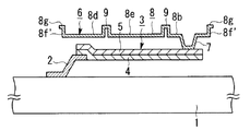
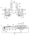
図8は、本発明の第5の実施の形態による静電容量型の放射検出装置の単位画素(単位素子)を示す図であり、図8(a)はその概略平面図、図8(b)は図8(a)中のY1−Y2線に沿った概略断面図である。
【0093】
本実施の形態による放射検出装置は、基体としてのSi基板等の基板41と、基板41から立ち上がった2つの脚部42,43と、赤外線iを吸収する赤外線吸収部44と、脚部42,43を介して基板41に支持され、赤外線吸収部44にて発生した熱に応じて基板41に対して変位する変位部45,46と、該変位部45,46の先端部分に接続された部材50と、を備えている。
【0094】
図8中、42a,43aは、脚部42,43における基板41へのコンタクト部をそれぞれ示している。脚部42,43の平面部42b,43bは、それぞれL字状に構成されている。脚部42,43は、断熱性の高い材料として、例えば、SiO膜で構成される。
【0095】
変位部45,46はそれぞれ、互いに重なった2つの膜48,49で構成されている。変位部45,46は、それらの一方端部が脚部42,43の平面部42b,43bの先端部分にそれぞれ接続されて支持されることにより、それぞれカンチレバーを構成しており、基板1上に浮いた状態に支持されている。膜48及び膜49は、互いに異なる膨張係数を有する異なる物質で構成されており、変位部45,46はそれぞれ、いわゆる熱バイモルフ構造(bi-material elementともいう。)を構成している。したがって、変位部45,46は、受けた熱に応じて、下側の膜48の膨張係数が上側の膜49の膨張係数より大きい場合には上方に、逆の場合には下方に湾曲して傾斜する。本実施の形態では、膜48は例えば厚さ3000オングストロームのSiN膜で構成され、膜49は例えば厚さ1000オングストロームのAl膜で構成されている。
【0096】
部材50は、Al膜49が変位部45,46からそのまま延びることによって構成されている。この部材50は、変位部45,46に生じた変位に応じた静電容量の変化を得るために用いられる変位読み出し部材としての可動電極部となっている。また、部材50は、赤外線iを略々全反射する赤外線反射部となっている。すなわち、本実施の形態では、赤外線反射部は可動電極部として兼用されている。なお、部材50における後述する赤外線吸収部44との対向面に赤外線反射部としての反射膜を形成し、部材50を可動電極部のみとして用いることもできる。
【0097】
赤外線吸収部44は、入射した赤外線iの一部を反射する特性を有している。赤外線吸収部5の赤外線反射率は、約33%であることが好ましい。赤外線吸収部44は、前記第1の実施の形態における反射板6と同様の薄膜部材で構成され、1層の膜からなる平面部51と、平面部51に混在するように形成され平面部51の下面側(裏面側)に突出した凸条部52とから構成されている。ただし、赤外線吸収部44は、前記第1の実施の形態における反射板6と異なり、立ち下がり部8fに相当する立ち下がり部は形成されていない。もっとも、このような立ち下がり部を形成してもよいことは、言うまでもない。赤外線吸収部44の断面構造は、例えば、図1(a)、図4、図5、図6のうちのいずれの反射板6の断面構造と同様にしてもよいし、凸条部52の平面視でのパターンは、例えば、図7中のいずれのパターンと同様にしてもよい。
【0098】
赤外線吸収部44の4箇所(1箇所以上であればよい。)の部分が接続部53を介して部材50に固定されることにより、部材50の上方に間隔(部材50と赤外線吸収部44の平面部53との間の間隔)L1をあけて部材50と実質的に平行に配置されている。本実施の形態では、赤外線吸収部44の各部及び接続部53は、例えば厚さ3000オングストロームのSiN膜で一体に形成されている。
【0099】
前記間隔L1は、nを奇数、入射赤外線iの所望の波長域の中心波長をλ0として、実質的にnλ0/4となるように設定されている。本実施の形態では、具体的には、λ0を10μm、nを1として、間隔L1は約2.5μmに設定されているが、これに限定されるものではない。
【0100】
基板41には、可動電極部としての部材50と対向するように、金属膜からなる固定電極部54が設けられている。固定電極部54の上面は、必要に応じて誘電体膜で覆ってもよい。また、基板41には、この固定電極部54の下側にこの電極54と電気的に接続された拡散層55が形成されるとともに、脚部42,43のコンタクト部42a,43a付近の下側に拡散層56が形成されている。脚部42,43上にはそれぞれ、Al膜49と拡散層56との間(ひいては、可動電極部としての部材50と拡散層56との間)を電気的に接続する配線層57が形成されている。コンタクト部42a,43aにはそれぞれ開口が形成され、これらの開口を介して配線層57が拡散層56と電気的に接続されるようになっている。
【0101】
本実施の形態による放射検出装置は、前述した第1の実施の形態と同様に、膜の形成及びパターニング、犠牲層の形成及び除去などの半導体製造技術を利用して、製造することができる。
【0102】
本実施の形態による放射検出装置では、上方から目標物体からの赤外線iが入射すると、入射した赤外線iは赤外線吸収部44で一部吸収され、残りは赤外線反射部としての部材50で反射され赤外線吸収部44で反射し再度部材50に入射する。このため、赤外線吸収部44と部材50との間で干渉現象が起こり、両者の間隔L1が入射赤外線iの所望の波長域の中心波長の1/4の略奇数倍とされているので、赤外線吸収部44での赤外線吸収がほぼ最大となり、赤外線吸収部44における赤外線の吸収率が高まる。したがって、赤外線吸収部44の厚みを薄くしてその熱容量を小さくしても、赤外線の吸収率を高めることができる。その結果、検出感度及び検出応答性の両方を高めることができる。
【0103】
そして、赤外線吸収部44で発生した熱が変位部45,46に伝わり、この熱に応じてカンチレバーを構成している変位部45,46が下方に湾曲して傾斜する。このため、部材50が、赤外線吸収部44との相対的な位置関係(すなわち、間隔L1)を保ったまま、入射した赤外線iの量に応じた量だけ基板41の面に対して傾き、可動電極部としての部材50と固定電極部54との間の距離が変化する。これにより、部材50と固定電極部54との間の静電容量の値が変化し、入射赤外線量を拡散層55,56間から静電容量の変化として検出することができる。なお、図面には示していないが、拡散層55,56はその静電容量を読み出す読み出し回路に接続されている。
【0104】
なお、図面には示していないが、変位部45,46、脚部42,43、電極部50,54及び赤外線吸収部44を単位素子(画素)として、この画素が基板41上に1次元状又は2次元状に配置されており、前記読み出し回路から赤外線画像信号が得られる。
【0105】
また、本実施の形態では、前述したように、赤外線吸収部44が前記第1の実施の形態における反射板6と同様の薄膜部材で構成されているので、赤外線吸収部44の所望の機械的強度を確保しつつ、赤外線吸収部44の膜厚を薄くすることができる。このため、この点からも、赤外線吸収部44の軽量化を図ることができるので、検出感度及び検出応答性を高めることができる。
【0106】
本実施の形態では、部材50は平面部のみで構成されているが、放射吸収部44と同様に、平面部と該平面部に混在するように形成された凸条部とを有する薄膜部材で構成してもよい。
【0107】
また、本実施の形態を次のように変形して、光読み出し型の放射検出装置としてもよい。すなわち、拡散領域55,56、固定電極54及び配線層57を取り除き、部材44をAl膜で構成し、この部材44に、上方から入射する読み出し光を反射する反射板、及び、基板41を透過して下方から入射する赤外線をほぼ反射する赤外線反射部、を兼用させる。そして、膜49をSiN膜で構成して、部材50を赤外線吸収部とする。この場合、部材50も、平面部と該平面部に混在するように形成された凸条部とを有する薄膜部材で構成してもよい。
【0108】
以上、本発明の各実施の形態やその変形例について説明したが、本発明はこれらに限定されるものではない。例えば、膜の材料や寸法等は前述したものに限定されない。
【0109】
前記第1乃至第4の実施の形態は、本発明による薄膜部材を光読み出し型の放射検出装置の反射板に適用した例であり、前記第5の実施の形態は、本発明による薄膜部材を静電容量型の放射検出装置の赤外線吸収部や赤外線反射部に適用した例であったが、本発明による薄膜部材の用途はこれらに限定されるものではなく、マイクロマシンや微少な素子を有する各種のデバイスなどにおいて用いることができる。
【0110】
【発明の効果】
以上説明したように、本発明によれば、所望の機械的強度を確保しつつ膜厚を薄くすることができる薄膜部材を提供することができる。
【0111】
また、本発明によれば、所望の機械的強度を確保しつつ膜厚を薄くすることができる薄膜部材を用いることによって、感度等の特性の向上を図ることができる放射検出装置を提供することができる。
【図面の簡単な説明】
【図1】本発明の第1の実施の形態による放射検出装置の単位画素を示す図である。
【図2】図1に示す放射検出装置の製造工程を示す概略断面図である。
【図3】図1に示す放射検出装置を用いた映像化装置の一例を示す概略構成図である。
【図4】本発明の第2の実施の形態による放射検出装置の単位画素を示す概略断面図である。
【図5】本発明の第3の実施の形態による放射検出装置の単位画素を示す概略断面図である。
【図6】本発明の第4の実施の形態による放射検出装置の単位画素を示す概略断面図である。
【図7】平面視での凸条部のパターンの各例を模式的に示す図である。
【図8】本発明の第5の実施の形態による静電容量型の放射検出装置の単位画素を示す図である。
【符号の説明】
1,41 基板
2,42,43 脚部
3,45,46 変位部
6 反射板
8,51 平面部
8a〜8e 平面部の領域
8f 立ち下がり部
8f’ 立ち上がり部
9,52 凸条部
44 赤外線吸収部
50 部材
54 固定電極[0001]
BACKGROUND OF THE INVENTION
The present invention relates to a thin film member used in various devices having micromachines and minute elements, and a radiation detection apparatus using the thin film member.
[0002]
[Prior art]
2. Description of the Related Art Conventionally, in a micromachine, various devices having minute elements, and the like, a thin film member having a flat plate portion supported so as to be positioned in the air has been used. This thin film member is generally manufactured using a semiconductor manufacturing process.
[0003]
For example, an optical readout type thermal radiation detection apparatus disclosed in Japanese Patent Application Laid-Open No. 2000-9542 is applied to the base according to heat generated in a base and a radiation absorption part supported by the base and absorbing radiation. A displacement portion that is displaced with respect to the displacement portion and a reading light reflection plate fixed to the displacement portion are provided, and the thin film member is used as the reflection plate.
[0004]
In the conventional thin film member as described above, the flat plate portion is simply composed of only a flat portion made of one or more layers having a desired flat shape.
[0005]
[Problems to be solved by the invention]
In the conventional thin film member, since the flat plate portion is composed only of a plane portion made of one or more layers having a desired plane shape, the film thickness is set to ensure a desired mechanical strength. I had to make it thicker. In particular, when the area of the flat plate portion is relatively large, the film thickness has to be considerably increased. For this reason, in the conventional thin film member, various inconveniences occurred depending on the application.
[0006]
This invention is made | formed in view of such a situation, and it aims at providing the thin film member which can make a film thickness thin, ensuring desired mechanical strength.
[0007]
Another object of the present invention is to provide a radiation detection device that can improve characteristics such as sensitivity by using a thin film member that can reduce the film thickness while ensuring a desired mechanical strength. And
[0008]
[Means for Solving the Problems]
In order to solve the above-described problem, the thin film member according to the first aspect of the present invention is a thin film member including a flat plate portion supported so as to be positioned in the air, and the flat plate portion includes one layer or a plurality of flat plate portions. The flat part which consists of a film | membrane of a layer, and the protruding item | line part which was formed so that it might be mixed in this flat part, and protruded in the surface side or the back surface side of the said flat part. Here, “mixed” means that the ridges are mixed with the flat part, and the ridges are not necessarily mixed with the flat part, and the ridges are simply mixed with the flat part. It may be mixed in various forms. The thin film member according to the first aspect is usually manufactured using a semiconductor manufacturing process.
[0009]
According to the first aspect, the flat plate portion has not only the flat surface portion but also the convex strip portion mixed therein, so that the flat surface portion is reinforced by the convex strip portion. Accordingly, the film thickness of the flat plate portion can be reduced while ensuring the desired mechanical strength of the flat plate portion.
[0010]
In addition, when the planar portion is composed of a plurality of layers of film, even if the planar portion is displaced due to a temperature change due to the difference in the expansion coefficient between the films of each layer, the displacement is blocked by the ridges, and the flatness of the planar portion is reduced. Will be maintained.
[0011]
The thin film member according to a second aspect of the present invention is the thin film member according to the first aspect, wherein the ridge portion is formed so as to substantially divide the planar portion into a plurality of regions.
When the ridges are formed as in the second aspect, the area of each region of the plane part substantially divided by the ridges is reduced, so that the mechanical strength of the flat plate part is improved. preferable.
[0012]
The thin film member according to a third aspect of the present invention is the thin film member according to the first or second aspect, wherein the protruding portion is one or more regions separated from the flat portion by a peripheral portion of the flat plate portion, And it forms so that a part of peripheral part of each said area | region may be substantially divided into the some area | region used as a part of peripheral part of the said flat plate-shaped part.
[0013]
As in the third aspect, when the ridge is formed so as to substantially divide the plane portion into one or more regions closer to the center and a plurality of regions closer to the periphery, Combined with the reduction of the area of the individual areas of the sectioned plane part, it becomes easy to realize the arrangement of the ridges as in the fourth aspect to be described later. It is preferable in terms of improvement.
[0014]
The thin film member according to the fourth aspect of the present invention is the thin film member according to any one of the first to third aspects, wherein each of the ridges is about each imaginary straight line connecting any two points of the peripheral portion of the flat plate part. The ridges are formed so as not to be located over the entire virtual straight line.
[0015]
As a result of the inventor's experiment, when the ridge is formed so as to be located over the entire virtual straight line connecting two points (for example, a point and a point opposite to this point) in the peripheral portion of the flat plate portion, While the flat plate portion is easily bent along the straight line, if the ridge portion is formed as in the fourth aspect, such a bend hardly occurs and the mechanical strength of the flat plate portion is improved. It turned out to be preferable.
[0016]
The thin film member according to the fifth aspect of the present invention is the thin film member according to any one of the first to fourth aspects, wherein the protruding line portion includes a curved portion.
[0017]
If the protruding portion includes a curved portion as in the fifth aspect, it is easy to realize the arrangement of the protruding portion as in the fourth aspect. It is preferable for improving the strength.
[0018]
The thin film member according to a sixth aspect of the present invention is the thin film member according to any one of the first to fifth aspects, wherein at least a part of the cross-sectional shape of the protrusion is substantially U-shaped so as to open on the side opposite to the protruding side. Or have a substantially solid shape.
[0019]
The sixth aspect is an example of the cross-sectional shape of the ridge portion, but the first to fifth aspects are not limited to this example.
[0020]
The thin film member according to a seventh aspect of the present invention is the thin film member according to any one of the first to sixth aspects, wherein the ridge portion is continuously formed of the same material from at least one layer of the film constituting the planar portion. It is formed integrally.
[0021]
According to the seventh aspect, the ridges can be formed at the same time when forming the film of at least one layer of the flat part, so that the manufacture is facilitated. But in the said 1st thru | or 6th aspect, you may form a protruding item | line part with a material different from a plane part, for example.
[0022]
A thin film member according to an eighth aspect of the present invention is the thin film member according to any one of the first to seventh aspects, wherein at least a part of a peripheral portion of each region of the planar portion is a peripheral portion of the flat plate portion. A rising portion or falling portion that rises or falls from the plane portion is formed.
[0023]
According to the eighth aspect, the flat plate portion is also reinforced by the rising portion or the falling portion. Therefore, the film thickness of the flat plate portion can be further reduced while ensuring the desired mechanical strength of the flat plate portion.
[0024]
A radiation detection apparatus according to a ninth aspect of the present invention includes a base body, a displacement portion that is supported by the base body and that is displaced with respect to the base body in response to heat generated in the radiation absorption section that absorbs radiation, and the displacement In a radiation detection apparatus comprising a displacement readout member fixed to a part, the displacement readout member being used to obtain a predetermined change in accordance with the displacement generated in the displacement part, the displacement readout member The thin film member according to any one of the first to eighth aspects is used.
[0025]
According to the ninth aspect, since the displacement reading member is constituted by the thin film member according to any one of the first to eighth aspects, the displacement reading member is secured while ensuring the desired mechanical strength of the displacement reading member. The film thickness of the member can be reduced. For this reason, since the weight of the displacement reading member can be reduced, the mechanical strength of the displacement portion can be reduced, and the thickness of the displacement portion can be reduced. The displacement portion usually has a structure having at least two layers of different substances having different expansion coefficients that are overlapped with each other. However, the thinner the displacement portion, the greater the displacement amount with respect to the temperature change and the higher the sensitivity. Therefore, according to the ninth aspect, it is possible to increase the sensitivity of the displacement portion, and consequently increase the sensitivity of radiation detection. In addition, since the thickness of the displacement reading member fixed to the displacement portion can be reduced, the overall heat capacity is reduced. For this reason, the responsiveness with respect to heat increases, and as a result, the responsiveness with respect to the change of the radiation to be detected increases.
[0026]
In the ninth aspect, the displacement readout member may be, for example, a reflection plate that reflects received readout light or an electrode. The former is an example in which the ninth aspect is applied to a so-called optical readout type radiation detection device that reads out the amount of incident radiation as a change in readout light. The latter is an example in which the ninth aspect is applied to a capacitance-type radiation detection device that reads the amount of incident radiation as a change in capacitance. However, the ninth aspect is not limited to these types of radiation detection devices. These points are the same for the tenth aspect described later. The thin film member according to the first to eighth aspects can be applied to a light receiving portion of a bolometer element, for example.
[0027]
In the radiation detection apparatus according to the ninth aspect, a plurality of the elements may be provided with the displacement portion and the displacement reading member as one element, and the elements may be arranged in a one-dimensional or two-dimensional manner. In this case, an image of radiation can be visualized. However, in the ninth aspect, only one pair of a displacement portion and a displacement readout member may be provided. These points are the same for the tenth aspect described later. In the ninth aspect, since the shape of the readout member is stabilized, when a plurality of the elements are provided, the variation in the shape of the readout member between the elements is reduced, so that the displacement between the elements is reduced. There is also an effect that the variation in the readout characteristics is reduced, and consequently, the variation in the radiation detection characteristics between the elements is reduced.
[0028]
A radiation detection apparatus according to a tenth aspect of the present invention includes a base body and a displacement portion that is supported by the base body and that displaces relative to the base body in response to heat generated in a radiation absorption section that absorbs radiation. In the radiation detection apparatus, the radiation absorption unit has a characteristic of reflecting a part of incident radiation, n is an odd number, and a center wavelength of a desired wavelength region of the radiation is λ. 0 Substantially from the radiation absorbing portion 0 Thin film member according to any one of the first to eighth aspects, wherein the thin film member is provided with a radiation reflection part arranged at a distance of / 4 and substantially totally reflecting the radiation, wherein at least one of the radiation absorption part and the radiation reflection part It is composed of
[0029]
According to the tenth aspect, when radiation is incident on the radiation absorbing portion from the side opposite to the radiation reflecting portion, the incident radiation is partially absorbed by the radiation absorbing portion, and the rest is reflected by the radiation reflecting portion and is reflected by the radiation absorbing portion. The light is reflected and enters the radiation reflection portion again. For this reason, an interference phenomenon occurs between the radiation absorbing portion and the radiation reflecting portion, and the distance between the two is set to approximately an odd multiple of 1/4 of the center wavelength of the desired wavelength range of the incident radiation. The radiation absorption at the point is almost maximized, and the radiation absorption rate in the radiation absorption part is increased. Therefore, even if the thickness of the radiation absorbing portion is reduced to reduce its heat capacity, the radiation absorption rate can be increased. As a result, both detection sensitivity and detection responsiveness can be improved. It is preferable to set the reflectance of the radiation absorbing portion to about 33% (about 1/3) because the radiation absorption rate in the radiation absorbing portion is further increased.
[0030]
In the tenth aspect, since at least one of the radiation absorption part and the radiation reflection part is formed of the thin film member according to any one of the first to eighth aspects, the radiation absorption part and the radiation reflection part are desired. It is possible to reduce the film thickness of the radiation absorbing portion and the radiation reflecting portion while ensuring the mechanical strength. For this reason, since it is possible to reduce the weight of the radiation absorbing portion and the radiation reflecting portion, even when the radiation absorbing portion and the radiation reflecting portion are provided so as to be supported directly or indirectly by the displacement portion, The mechanical strength of the displacement part can be reduced, and the film thickness of the displacement part can be reduced. Therefore, according to the tenth aspect, similarly to the ninth aspect, it is possible to increase the sensitivity of the displacement portion, and consequently to increase the sensitivity of radiation detection. Further, according to the tenth aspect, since the film thickness of the radiation absorbing portion and the radiation reflecting portion can be reduced, the radiation absorbing portion and the radiation reflecting portion are directly or indirectly fixed to the displacement portion. In this case, the overall heat capacity is reduced. For this reason, the responsiveness with respect to heat increases, and as a result, the responsiveness with respect to the change of the radiation to be detected increases. In addition, it cannot be overemphasized that the matter of the said 9th aspect may be comprised in the said 10th aspect.
[0031]
The ninth and tenth aspects are examples in which the thin film member according to the first to eighth aspects is used in a radiation detection device, but the thin film member according to the first to eighth aspects is other It can also be used in various devices and micromachines.
[0032]
DETAILED DESCRIPTION OF THE INVENTION
In the following description, an example in which the radiation is infrared and the readout light is visible light will be described. However, in the present invention, the radiation may be X-rays other than infrared rays, ultraviolet rays, and other various types of radiation. May be other light than visible light.
[0033]
[First Embodiment]
[0034]
FIG. 1 is a diagram showing a unit pixel (unit element) of an optical readout type
[0035]
The
[0036]
The
[0037]
In the present embodiment, the
[0038]
A part of the
[0039]
In the present embodiment, as shown in FIG. 1A, the
[0040]
Furthermore, in the present embodiment, of the peripheral portions of the
[0041]
In the present embodiment, the
[0042]
Although not shown in the drawing, the
[0043]
Next, an example of a method for manufacturing the
[0044]
First, as shown in FIG. 2A, a resist 10 as a sacrificial layer is applied to the entire surface of the
[0045]
Next, a resist 11 as a sacrificial layer is applied to the entire surface of the substrate in the state shown in FIG. 2A, and an
[0046]
Thereafter, a
[0047]
Next, on the substrate in the state shown in FIG. 2 (c), an Al film (for example, a thickness of 2000 angstroms) to be the
[0048]
Finally, the substrate in the state shown in FIG. 2D is divided into chips by dicing or the like, and the resists 10 and 11 and the
[0049]
According to the present embodiment, the flat plate portion constituting the reflecting
[0050]
Thus, since the film thickness (especially film thickness of the plane part 8) of the reflecting
[0051]
Moreover, according to this Embodiment, since the film thickness of the reflecting
[0052]
Furthermore, according to this Embodiment, since the flat plate-shaped part which comprises the reflecting
[0053]
Furthermore, according to the present embodiment, since the
[0054]
Here, an example of an imaging apparatus using the
[0055]
In addition to the
[0056]
In this imaging apparatus, the readout optical system includes an LD (laser diode) 23 as readout light supply means for supplying readout light, and reflectors of all the pixels of the
[0057]
The
[0058]
The beam
[0059]
According to the imaging apparatus shown in FIG. 3, the
[0060]
On the other hand, infrared rays from the heat source (target object) 21 are collected by the
[0061]
Now, it is assumed that the infrared rays from the
[0062]
Now, it is assumed that a certain amount of infrared light is incident on the
[0063]
Therefore, the optical image by the readout light formed on the light receiving surface of the
[0064]
Needless to say, the configuration of the readout optical system is not limited to the configuration described above.
[0065]
The above is an example of an imaging device. In FIG. 3, a radiation detection device having only a single pixel (element) is used as the
[0066]
[Second Embodiment]
[0067]
FIG. 4 is a schematic sectional view showing a unit pixel (unit element) of an optical readout type radiation detection apparatus according to the second embodiment of the present invention, and corresponds to FIG. 4, elements that are the same as or correspond to those in FIG. 1 are given the same reference numerals, and redundant descriptions thereof are omitted.
[0068]
The present embodiment is different from the first embodiment only in that the uneven structure of the
[0069]
Also in this embodiment, the same advantages as those in the first embodiment can be obtained.
[0070]
[Third Embodiment]
[0071]
FIG. 5 is a schematic sectional view showing a unit pixel (unit element) of an optical readout type radiation detection apparatus according to the third embodiment of the present invention, and corresponds to FIG. 5, elements that are the same as or correspond to those in FIG. 1 are given the same reference numerals, and redundant descriptions thereof are omitted.
[0072]
The present embodiment is different from the first embodiment only in that the cross-sectional shape of the
[0073]
Also in this embodiment, the same advantages as those in the first embodiment can be obtained.
[0074]
[Fourth Embodiment]
[0075]
FIG. 6 is a schematic cross-sectional view showing a unit pixel (unit element) of an optical readout type radiation detection apparatus according to the fourth embodiment of the present invention, and corresponds to FIG. In FIG. 6, the same or corresponding elements as those in FIG. 1 are denoted by the same reference numerals, and redundant description thereof is omitted.
[0076]
The difference between the present embodiment and the first embodiment is that, in the
[0077]
Also in this embodiment, the same advantages as those in the first embodiment can be obtained.
[0078]
[Pattern pattern example]
[0079]
In the first to fifth embodiments, the pattern of the
[0080]
In the first to fourth embodiments described above, the pattern of the
[0081]
As already described, the strength is greatly improved in the patterns shown in FIGS. 1 (a) and 7 (b). It has been found by experiments of the present inventor that the strength is greatly improved in the case of such a pattern.
[0082]
In the patterns shown in FIGS. 7B to 7D, the shape of the central region of the
[0083]
Each of the patterns shown in FIGS. 7 (e) and 7 (f) has five regions (regions near the center) separated from the peripheral portion of the plate-like portion among the regions of the plate-like portion divided by the
[0084]
The pattern shown in FIG. 7 (g) is obtained by rearranging the portions of the
[0085]
The pattern shown in FIG. 7 (h) is basically the same as the pattern shown in FIG. 1 (a) and FIG. 7 (a), but the shape of the flat plate portion is the same as that shown in FIG. 1 (a) and FIG. In the case of), the corners of the flat plate portion are chamfered. Even if it is the external shape of this flat part, and the pattern of the protruding item |
[0086]
In the pattern shown in FIG. 7 (i), the
[0087]
FIG. 7 (j) shows an example of the pattern of the
[0088]
The pattern shown in FIG. 7 (k) is basically the same as the pattern shown in FIG. 1 (a) and FIG. 7 (a), but the
[0089]
In the patterns shown in FIGS. 7A to 7K, the
[0090]
As shown in the patterns of FIGS. 7 (b), (c), (g), and (n), when the
[0091]
[Fifth Embodiment]
[0092]
FIG. 8 is a diagram showing a unit pixel (unit element) of a capacitance type radiation detection apparatus according to the fifth embodiment of the present invention. FIG. 8A is a schematic plan view thereof, and FIG. ) Is a schematic cross-sectional view taken along line Y1-Y2 in FIG.
[0093]
The radiation detection apparatus according to the present embodiment includes a
[0094]
In FIG. 8,
[0095]
The
[0096]
The
[0097]
The infrared absorbing
[0098]
By fixing the four portions (one or more may be sufficient) of the infrared absorbing
[0099]
The interval L1 is an odd number n, and a center wavelength of a desired wavelength region of the incident infrared ray i is λ. 0 As substantially nλ 0 / 4 is set. In the present embodiment, specifically, λ 0 Is 10 μm, n is 1, and the interval L1 is set to about 2.5 μm. However, the present invention is not limited to this.
[0100]
The
[0101]
The radiation detection apparatus according to the present embodiment can be manufactured using a semiconductor manufacturing technique such as film formation and patterning and sacrificial layer formation and removal, as in the first embodiment.
[0102]
In the radiation detection apparatus according to the present embodiment, when the infrared ray i from the target object is incident from above, the incident infrared ray i is partially absorbed by the infrared absorbing
[0103]
Then, the heat generated in the infrared absorbing
[0104]
Although not shown in the drawing, the
[0105]
In the present embodiment, as described above, since the infrared absorbing
[0106]
In the present embodiment, the
[0107]
Further, the present embodiment may be modified as follows to provide an optical readout type radiation detection apparatus. That is, the
[0108]
As mentioned above, although each embodiment of this invention and its modification were demonstrated, this invention is not limited to these. For example, the material and dimensions of the film are not limited to those described above.
[0109]
The first to fourth embodiments are examples in which the thin film member according to the present invention is applied to a reflector of an optical readout type radiation detection device, and the fifth embodiment is a thin film member according to the present invention. Although it was an example applied to the infrared absorption part and the infrared reflection part of the capacitance type radiation detection device, the use of the thin film member according to the present invention is not limited to these, and various kinds of devices including a micromachine and a minute element It can be used in such devices.
[0110]
【The invention's effect】
As described above, according to the present invention, it is possible to provide a thin film member capable of reducing the film thickness while ensuring a desired mechanical strength.
[0111]
In addition, according to the present invention, it is possible to provide a radiation detection apparatus capable of improving characteristics such as sensitivity by using a thin film member capable of reducing a film thickness while ensuring a desired mechanical strength. Can do.
[Brief description of the drawings]
FIG. 1 is a diagram showing a unit pixel of a radiation detection apparatus according to a first embodiment of the present invention.
FIG. 2 is a schematic cross-sectional view showing a manufacturing process of the radiation detection apparatus shown in FIG.
FIG. 3 is a schematic configuration diagram showing an example of an imaging apparatus using the radiation detection apparatus shown in FIG. 1;
FIG. 4 is a schematic cross-sectional view showing a unit pixel of a radiation detection apparatus according to a second embodiment of the present invention.
FIG. 5 is a schematic cross-sectional view showing a unit pixel of a radiation detection apparatus according to a third embodiment of the present invention.
FIG. 6 is a schematic cross-sectional view showing a unit pixel of a radiation detection apparatus according to a fourth embodiment of the present invention.
FIG. 7 is a diagram schematically showing each example of a pattern of ridges in a plan view.
FIG. 8 is a diagram showing a unit pixel of a capacitance type radiation detection apparatus according to a fifth embodiment of the present invention.
[Explanation of symbols]
1,41 substrate
2,42,43 legs
3, 45, 46 Displacement part
6 reflector
8,51 plane part
8a-8e Plane area
8f Falling part
8f 'rising part
9,52 ridge
44 Infrared absorber
50 members
54 Fixed electrode
Claims (4)
第一の犠牲層を形成する工程と、
前記第一の犠牲層に、前記平板状部を空中に支持するための接続部に応じた開口を形成する工程と、
前記第一の犠牲層上に第二の犠牲層を形成する工程と、
前記第二の犠牲層に、前記接続部及び前記凸条部に応じた開口を形成する工程と、
前記平板状部及び前記接続部を構成する薄膜を形成する工程と、
前記第一及び第二の犠牲層を除去する工程と、
を有し、
前記凸条部は、前記平面部を、前記平板状部の周辺部分から隔てられた1つ以上の領域、及び、当該各領域の周辺部分の一部が前記平板状部の周辺部分の一部となる複数の領域に、区分するように、形成され、
前記凸条部は、前記平板状部の周辺部分の任意の2点を結ぶ各仮想直線について、当該仮想直線の全体に渡っては前記凸条部が位置することがないように、形成され、
前記平面部及び前記凸条部は、互いに同じ層数の層からなる膜が互いに連続して形成されたものであることを特徴とする薄膜部材の製造方法。The flat plate portion is supported so as to be positioned in the air, and the flat plate portion is formed so as to be mixed in the flat portion and the flat portion formed of one or a plurality of layers. Or a method for producing a thin film member having a protruding portion protruding on the back side,
Forming a first sacrificial layer;
Forming an opening in the first sacrificial layer according to a connection portion for supporting the flat plate-like portion in the air;
Forming a second sacrificial layer on the first sacrificial layer;
Forming an opening in the second sacrificial layer in accordance with the connection portion and the ridge portion;
Forming a thin film constituting the flat plate portion and the connection portion;
Removing the first and second sacrificial layers;
I have a,
The projecting ridge portion includes one or more regions separated from the peripheral portion of the flat plate portion, and a part of the peripheral portion of each region is a part of the peripheral portion of the flat plate portion. Is formed to be divided into a plurality of regions,
The ridge portion is formed so that the ridge portion is not positioned over the entire virtual straight line for each virtual straight line connecting any two points of the peripheral portion of the flat plate portion,
The method for producing a thin film member, wherein the planar portion and the ridge portion are formed by continuously forming films having the same number of layers .
Priority Applications (1)
| Application Number | Priority Date | Filing Date | Title |
|---|---|---|---|
| JP2000344125A JP4649727B2 (en) | 2000-11-10 | 2000-11-10 | Method for manufacturing thin film member |
Applications Claiming Priority (1)
| Application Number | Priority Date | Filing Date | Title |
|---|---|---|---|
| JP2000344125A JP4649727B2 (en) | 2000-11-10 | 2000-11-10 | Method for manufacturing thin film member |
Publications (2)
| Publication Number | Publication Date |
|---|---|
| JP2002148120A JP2002148120A (en) | 2002-05-22 |
| JP4649727B2 true JP4649727B2 (en) | 2011-03-16 |
Family
ID=18818376
Family Applications (1)
| Application Number | Title | Priority Date | Filing Date |
|---|---|---|---|
| JP2000344125A Expired - Fee Related JP4649727B2 (en) | 2000-11-10 | 2000-11-10 | Method for manufacturing thin film member |
Country Status (1)
| Country | Link |
|---|---|
| JP (1) | JP4649727B2 (en) |
Families Citing this family (2)
| Publication number | Priority date | Publication date | Assignee | Title |
|---|---|---|---|---|
| WO2011080883A1 (en) * | 2009-12-28 | 2011-07-07 | 株式会社ニコン | Electro-mechanical converter, spatial optical modulator, exposure device, and methods for manufacturing them |
| JP5630015B2 (en) * | 2009-12-28 | 2014-11-26 | 株式会社ニコン | Spatial light modulator, exposure apparatus and manufacturing method thereof |
Family Cites Families (10)
| Publication number | Priority date | Publication date | Assignee | Title |
|---|---|---|---|---|
| JPS61262303A (en) * | 1985-05-16 | 1986-11-20 | Asahi Chem Ind Co Ltd | Microstrip array antenna |
| JPS6337999A (en) * | 1986-08-01 | 1988-02-18 | 理化学研究所 | IC card |
| JPH03243218A (en) * | 1990-02-20 | 1991-10-30 | Ishino Gasket Kogyo Kk | Working forming for metallic thin flat sheet |
| US5181156A (en) * | 1992-05-14 | 1993-01-19 | Motorola Inc. | Micromachined capacitor structure and method for making |
| JPH06174551A (en) * | 1992-12-03 | 1994-06-24 | Mitsuteru Kimura | Thermal photosensor |
| JPH0961234A (en) * | 1995-08-28 | 1997-03-07 | Matsushita Electric Works Ltd | Infrared-ray detecting element and its manufacture |
| JPH1088724A (en) * | 1996-09-12 | 1998-04-07 | Oyo Kikaku:Kk | Planar spring, composite planar spring, spring panel |
| JP2954933B2 (en) * | 1997-10-20 | 1999-09-27 | 株式会社ホクキャスト | Manhole cover |
| JPH11166859A (en) * | 1997-12-05 | 1999-06-22 | Nikon Corp | Optical readout radiation-to-displacement converter and imaging device using the same |
| JP2000186958A (en) * | 1998-12-24 | 2000-07-04 | Sharp Corp | Thermal infrared detector |
-
2000
- 2000-11-10 JP JP2000344125A patent/JP4649727B2/en not_active Expired - Fee Related
Also Published As
| Publication number | Publication date |
|---|---|
| JP2002148120A (en) | 2002-05-22 |
Similar Documents
| Publication | Publication Date | Title |
|---|---|---|
| JP4945861B2 (en) | Thermal displacement element and radiation detector using the same | |
| US6469301B1 (en) | Radiation detectors including thermal-type displaceable element with increased responsiveness | |
| JP3404607B2 (en) | Confocal optics | |
| US7851759B2 (en) | Infrared imaging apparatus | |
| WO1995009346A1 (en) | Confocal optical apparatus | |
| US7580175B2 (en) | Detector of infrared radiation having a bi-material transducer | |
| US9810581B1 (en) | Micromechanical device for electromagnetic radiation sensing | |
| JP3003853B2 (en) | Sensor with bridge structure | |
| JP4649727B2 (en) | Method for manufacturing thin film member | |
| JP4538862B2 (en) | Thermal displacement element and radiation detector | |
| US6828557B2 (en) | Radiation-detection devices | |
| JP4051830B2 (en) | Radiation detector | |
| JP2012154762A (en) | Infrared sensor and infrared sensor array | |
| US6307202B1 (en) | Bimorph spirals for uncooled photothermal spectroscopy | |
| JP2012208104A (en) | Semiconductor optical element and semiconductor optical device | |
| JP4337239B2 (en) | Radiation detector | |
| JP3790878B2 (en) | Thermal displacement element and radiation detector using the same | |
| JP2000221081A (en) | Thermal displacement element and radiation detection device using the same | |
| JP2002221449A (en) | Radiation detector | |
| JP2002168686A (en) | Radiation detector | |
| JP2000241240A (en) | Radiation-displacement converter and imaging device using the same | |
| JPH11166859A (en) | Optical readout radiation-to-displacement converter and imaging device using the same | |
| JP2007212345A (en) | Thin film structure, thermal displacement element and radiation detection apparatus using the same | |
| JP4700825B2 (en) | Optical encoder | |
| JPH0814887A (en) | Optical displacement gauge |
Legal Events
| Date | Code | Title | Description |
|---|---|---|---|
| A621 | Written request for application examination |
Free format text: JAPANESE INTERMEDIATE CODE: A621 Effective date: 20070827 |
|
| A977 | Report on retrieval |
Free format text: JAPANESE INTERMEDIATE CODE: A971007 Effective date: 20100112 |
|
| A131 | Notification of reasons for refusal |
Free format text: JAPANESE INTERMEDIATE CODE: A131 Effective date: 20100202 |
|
| AA91 | Notification that invitation to amend document was cancelled |
Free format text: JAPANESE INTERMEDIATE CODE: A971091 Effective date: 20100302 |
|
| A131 | Notification of reasons for refusal |
Free format text: JAPANESE INTERMEDIATE CODE: A131 Effective date: 20100316 |
|
| A521 | Request for written amendment filed |
Free format text: JAPANESE INTERMEDIATE CODE: A523 Effective date: 20100506 |
|
| A131 | Notification of reasons for refusal |
Free format text: JAPANESE INTERMEDIATE CODE: A131 Effective date: 20100713 |
|
| A521 | Request for written amendment filed |
Free format text: JAPANESE INTERMEDIATE CODE: A523 Effective date: 20100825 |
|
| TRDD | Decision of grant or rejection written | ||
| A01 | Written decision to grant a patent or to grant a registration (utility model) |
Free format text: JAPANESE INTERMEDIATE CODE: A01 Effective date: 20101116 |
|
| A01 | Written decision to grant a patent or to grant a registration (utility model) |
Free format text: JAPANESE INTERMEDIATE CODE: A01 |
|
| A61 | First payment of annual fees (during grant procedure) |
Free format text: JAPANESE INTERMEDIATE CODE: A61 Effective date: 20101129 |
|
| R150 | Certificate of patent or registration of utility model |
Ref document number: 4649727 Country of ref document: JP Free format text: JAPANESE INTERMEDIATE CODE: R150 Free format text: JAPANESE INTERMEDIATE CODE: R150 |
|
| FPAY | Renewal fee payment (event date is renewal date of database) |
Free format text: PAYMENT UNTIL: 20131224 Year of fee payment: 3 |
|
| FPAY | Renewal fee payment (event date is renewal date of database) |
Free format text: PAYMENT UNTIL: 20131224 Year of fee payment: 3 |
|
| R250 | Receipt of annual fees |
Free format text: JAPANESE INTERMEDIATE CODE: R250 |
|
| R250 | Receipt of annual fees |
Free format text: JAPANESE INTERMEDIATE CODE: R250 |
|
| R250 | Receipt of annual fees |
Free format text: JAPANESE INTERMEDIATE CODE: R250 |
|
| R250 | Receipt of annual fees |
Free format text: JAPANESE INTERMEDIATE CODE: R250 |
|
| R250 | Receipt of annual fees |
Free format text: JAPANESE INTERMEDIATE CODE: R250 |
|
| R250 | Receipt of annual fees |
Free format text: JAPANESE INTERMEDIATE CODE: R250 |
|
| LAPS | Cancellation because of no payment of annual fees |