JP4638806B2 - Phase-locked loop circuit, offset PLL transmitter, high-frequency integrated circuit for communication, and wireless communication system - Google Patents
Phase-locked loop circuit, offset PLL transmitter, high-frequency integrated circuit for communication, and wireless communication system Download PDFInfo
- Publication number
- JP4638806B2 JP4638806B2 JP2005326340A JP2005326340A JP4638806B2 JP 4638806 B2 JP4638806 B2 JP 4638806B2 JP 2005326340 A JP2005326340 A JP 2005326340A JP 2005326340 A JP2005326340 A JP 2005326340A JP 4638806 B2 JP4638806 B2 JP 4638806B2
- Authority
- JP
- Japan
- Prior art keywords
- circuit
- frequency
- output
- signal
- input
- Prior art date
- Legal status (The legal status is an assumption and is not a legal conclusion. Google has not performed a legal analysis and makes no representation as to the accuracy of the status listed.)
- Expired - Fee Related
Links
Images


Classifications
-
- H—ELECTRICITY
- H03—ELECTRONIC CIRCUITRY
- H03L—AUTOMATIC CONTROL, STARTING, SYNCHRONISATION, OR STABILISATION OF GENERATORS OF ELECTRONIC OSCILLATIONS OR PULSES
- H03L7/00—Automatic control of frequency or phase; Synchronisation
- H03L7/06—Automatic control of frequency or phase; Synchronisation using a reference signal applied to a frequency- or phase-locked loop
- H03L7/08—Details of the phase-locked loop
- H03L7/085—Details of the phase-locked loop concerning mainly the frequency- or phase-detection arrangement including the filtering or amplification of its output signal
- H03L7/089—Details of the phase-locked loop concerning mainly the frequency- or phase-detection arrangement including the filtering or amplification of its output signal the phase or frequency detector generating up-down pulses
- H03L7/0891—Details of the phase-locked loop concerning mainly the frequency- or phase-detection arrangement including the filtering or amplification of its output signal the phase or frequency detector generating up-down pulses the up-down pulses controlling source and sink current generators, e.g. a charge pump
- H03L7/0895—Details of the current generators
-
- H—ELECTRICITY
- H03—ELECTRONIC CIRCUITRY
- H03C—MODULATION
- H03C3/00—Angle modulation
- H03C3/02—Details
- H03C3/09—Modifications of modulator for regulating the mean frequency
- H03C3/0908—Modifications of modulator for regulating the mean frequency using a phase locked loop
- H03C3/0916—Modifications of modulator for regulating the mean frequency using a phase locked loop with frequency divider or counter in the loop
- H03C3/0933—Modifications of modulator for regulating the mean frequency using a phase locked loop with frequency divider or counter in the loop using fractional frequency division in the feedback loop of the phase locked loop
-
- H—ELECTRICITY
- H03—ELECTRONIC CIRCUITRY
- H03C—MODULATION
- H03C3/00—Angle modulation
- H03C3/02—Details
- H03C3/09—Modifications of modulator for regulating the mean frequency
- H03C3/0908—Modifications of modulator for regulating the mean frequency using a phase locked loop
- H03C3/0966—Modifications of modulator for regulating the mean frequency using a phase locked loop modulating the reference clock
-
- H—ELECTRICITY
- H03—ELECTRONIC CIRCUITRY
- H03C—MODULATION
- H03C3/00—Angle modulation
- H03C3/02—Details
- H03C3/09—Modifications of modulator for regulating the mean frequency
- H03C3/0908—Modifications of modulator for regulating the mean frequency using a phase locked loop
- H03C3/0983—Modifications of modulator for regulating the mean frequency using a phase locked loop containing in the loop a mixer other than for phase detection
-
- H—ELECTRICITY
- H03—ELECTRONIC CIRCUITRY
- H03C—MODULATION
- H03C3/00—Angle modulation
- H03C3/02—Details
- H03C3/09—Modifications of modulator for regulating the mean frequency
- H03C3/0908—Modifications of modulator for regulating the mean frequency using a phase locked loop
- H03C3/0991—Modifications of modulator for regulating the mean frequency using a phase locked loop including calibration means or calibration methods
-
- H—ELECTRICITY
- H03—ELECTRONIC CIRCUITRY
- H03L—AUTOMATIC CONTROL, STARTING, SYNCHRONISATION, OR STABILISATION OF GENERATORS OF ELECTRONIC OSCILLATIONS OR PULSES
- H03L7/00—Automatic control of frequency or phase; Synchronisation
- H03L7/06—Automatic control of frequency or phase; Synchronisation using a reference signal applied to a frequency- or phase-locked loop
- H03L7/08—Details of the phase-locked loop
- H03L7/085—Details of the phase-locked loop concerning mainly the frequency- or phase-detection arrangement including the filtering or amplification of its output signal
- H03L7/089—Details of the phase-locked loop concerning mainly the frequency- or phase-detection arrangement including the filtering or amplification of its output signal the phase or frequency detector generating up-down pulses
- H03L7/0891—Details of the phase-locked loop concerning mainly the frequency- or phase-detection arrangement including the filtering or amplification of its output signal the phase or frequency detector generating up-down pulses the up-down pulses controlling source and sink current generators, e.g. a charge pump
- H03L7/0895—Details of the current generators
- H03L7/0898—Details of the current generators the source or sink current values being variable
-
- H—ELECTRICITY
- H03—ELECTRONIC CIRCUITRY
- H03L—AUTOMATIC CONTROL, STARTING, SYNCHRONISATION, OR STABILISATION OF GENERATORS OF ELECTRONIC OSCILLATIONS OR PULSES
- H03L7/00—Automatic control of frequency or phase; Synchronisation
- H03L7/06—Automatic control of frequency or phase; Synchronisation using a reference signal applied to a frequency- or phase-locked loop
- H03L7/08—Details of the phase-locked loop
- H03L7/10—Details of the phase-locked loop for assuring initial synchronisation or for broadening the capture range
- H03L7/107—Details of the phase-locked loop for assuring initial synchronisation or for broadening the capture range using a variable transfer function for the loop, e.g. low pass filter having a variable bandwidth
- H03L7/1072—Details of the phase-locked loop for assuring initial synchronisation or for broadening the capture range using a variable transfer function for the loop, e.g. low pass filter having a variable bandwidth by changing characteristics of the charge pump, e.g. changing the gain
-
- H—ELECTRICITY
- H03—ELECTRONIC CIRCUITRY
- H03L—AUTOMATIC CONTROL, STARTING, SYNCHRONISATION, OR STABILISATION OF GENERATORS OF ELECTRONIC OSCILLATIONS OR PULSES
- H03L7/00—Automatic control of frequency or phase; Synchronisation
- H03L7/06—Automatic control of frequency or phase; Synchronisation using a reference signal applied to a frequency- or phase-locked loop
- H03L7/16—Indirect frequency synthesis, i.e. generating a desired one of a number of predetermined frequencies using a frequency- or phase-locked loop
- H03L7/18—Indirect frequency synthesis, i.e. generating a desired one of a number of predetermined frequencies using a frequency- or phase-locked loop using a frequency divider or counter in the loop
- H03L7/183—Indirect frequency synthesis, i.e. generating a desired one of a number of predetermined frequencies using a frequency- or phase-locked loop using a frequency divider or counter in the loop a time difference being used for locking the loop, the counter counting between fixed numbers or the frequency divider dividing by a fixed number
- H03L7/185—Indirect frequency synthesis, i.e. generating a desired one of a number of predetermined frequencies using a frequency- or phase-locked loop using a frequency divider or counter in the loop a time difference being used for locking the loop, the counter counting between fixed numbers or the frequency divider dividing by a fixed number using a mixer in the loop
Landscapes
- Stabilization Of Oscillater, Synchronisation, Frequency Synthesizers (AREA)
- Transmitters (AREA)
- Synchronisation In Digital Transmission Systems (AREA)
Description
本発明は、位相同期(PLL)回路のループ特性検出回路に係り、特に位相同期ループの回路のループ利得検出方式及びその検出方式に基づいたループ利得検出回路を備えたPLL回路を内蔵するオフセットPLL送信機、高周波集積回路及び無線通信システムに関する。 The present invention relates to a loop characteristic detection circuit of a phase locked loop (PLL) circuit, and more particularly, an offset PLL incorporating a loop gain detection system for a phase locked loop circuit and a PLL circuit having a loop gain detection circuit based on the detection system. The present invention relates to a transmitter, a high frequency integrated circuit, and a wireless communication system.
PLLを用いた送信回路として、例えば非特許文献1〜3に記載されたものがある。これらは、いずれも、フラクショナルN型PLLでループ帯域を校正する送受信システムである。
As a transmission circuit using a PLL, for example, there are those described in
まず、非特許文献1の送受信システムは、ループ帯域を検出するための信号としてベースバンドからのデータ信号で0101のパターンを入力して矩形波を作成し、この矩形波をフラクショナルN型PLLに入力している。ループ帯域の検出は、電圧制御型信号源の出力をモニタして行っている。
First, the transmission / reception system of Non-Patent
非特許文献2の送受信システムでは、ループ帯域を検出するための信号として送信中のデータ信号を用いている。検出方法としては、電圧制御型信号源の出力をモニタし、位相成分をデジタル化することで、ベースバンドからのデータ信号と比較し、さらに積分することでループ帯域を検出している。
In the transmission / reception system of Non-Patent
非特許文献3の発明は、フラクショナルN型のPLLにおけるループ帯域の校正システムを対象としている。ループ帯域を検出するための信号として、シグマデルタ変調器を介して、PLLにおける分周器にステップ信号を入力している。この場合、位相比較器における、フィードバック入力側の信号が状態遷移する。 The invention of Non-Patent Document 3 is directed to a loop band calibration system in a fractional N type PLL. As a signal for detecting a loop band, a step signal is input to a frequency divider in the PLL via a sigma delta modulator. In this case, the signal on the feedback input side in the phase comparator makes a state transition.
一方、非特許文献4には、Digital Frequency Locked Loopでループ帯域の校正を行う送受信システムが開示されている。この場合、キャリブレーション専用のチャージポンプ型DA変換器とループフィルタを使用し、電圧制御型電圧源に異なる2つの電圧を与え、そのときの周波数の変化から電圧制御型電圧源での利得を検出して、ループ帯域の校正を行っている。
On the other hand, Non-Patent
無線送信機では送信に用いられる周波数が決められており、隣接する周波数帯を用いる機器に悪影響を与えないために一定の周波数精度を持つことが要求される。すなわち、携帯・自動車電話では、多くの端末が同時に電波を利用するため、個々の端末は使用周波数を変えたり、時分割を行ったりしてお互いの干渉が無いように制御されている。例えばGSM(Global System for Mobile Communications)規格の携帯電話では、200kHz間隔でチャネルを設定して利用している。これによりVCOの発振周波数を200kHz刻みで設定することが必要になるが、分周比は整数であるため、VCOの周波数は基準周波数の整数倍の値しか取れず、細かな周波数設定ができない。このため、分周比を時間的に細かく変化させ、擬似的に中間の周波数を作り出す必要がある。この分周比を変化させる処理は、シグマデルタ変調と呼ばれる。 In a wireless transmitter, the frequency used for transmission is determined, and it is required to have a certain frequency accuracy so as not to adversely affect devices using adjacent frequency bands. In other words, since many terminals use radio waves at the same time in mobile / car telephones, individual terminals are controlled so as not to interfere with each other by changing the frequency used or performing time division. For example, a GSM (Global System for Mobile Communications) standard mobile phone uses a channel set at intervals of 200 kHz. This makes it necessary to set the oscillation frequency of the VCO in increments of 200 kHz. However, since the frequency division ratio is an integer, the VCO frequency can only be an integer multiple of the reference frequency, and fine frequency setting cannot be performed. For this reason, it is necessary to change the frequency division ratio finely in time to create a pseudo intermediate frequency. This process of changing the frequency division ratio is called sigma delta modulation.
携帯・自動車電話で要求される周波数精度は、高周波発振器の持つ精度を超えるものであるため、一般的には水晶発振器のような高い周波数精度を持つ素子を参照信号として、PLL回路を構成し、高周波発振器の周波数精度を向上している。PLL回路は、入力信号と回路に内蔵された発振器からの信号とを比較して、周波数や位相のずれを検知し、その誤差を発振器ヘフィードバックして出力信号を生成する。 Since the frequency accuracy required for mobile phones and car phones exceeds the accuracy of high-frequency oscillators, in general, a PLL circuit is configured using an element with high frequency accuracy such as a crystal oscillator as a reference signal. The frequency accuracy of the high-frequency oscillator is improved. The PLL circuit compares an input signal with a signal from an oscillator built in the circuit, detects a frequency or phase shift, and feeds back the error to the oscillator to generate an output signal.
従来、PLL回路に用いられるループフィルタ回路は、抵抗値や容量値などの素子数が大きいことに加え、LSIに集積化した場合、素子ばらつきの影響でアナログ精度が低減し校正精度の劣化を招くこと、回路規模が大きくなること、校正時問がかかってしまうことなどから、外付け部品が使われていた。 Conventional loop filter circuits used in PLL circuits have a large number of elements such as resistance values and capacitance values, and when integrated in an LSI, the analog accuracy is reduced due to the effect of element variations, leading to deterioration in calibration accuracy. In addition, external parts were used because of the increased circuit scale and the time required for calibration.
しかし、移動体通信機器は、より小型化することを常に求められている。外付け部品の削減は、移動体通信機器の集積化、小型化を促進する上での大きな課題の1つである。このため、校正精度を劣化させることなく、ループフィルタ回路をPLL回路に集積化できる技術の開発が求められている。 However, mobile communication devices are always required to be smaller. The reduction of external parts is one of the major issues in promoting the integration and miniaturization of mobile communication devices. For this reason, development of a technique capable of integrating the loop filter circuit in the PLL circuit without degrading the calibration accuracy is required.
外付け部品の削減策の一環としてループフィルタをIC内に内蔵する場合には、素子のバラツキが大きくなり、設計値からの差が顕著になる。すなわち、位相同期ループのループ帯域は、電圧制御型発振器の感度や、ループフィルタを構成する素子のバラツキにより、設計値から大きく外れることがある。GMC型のフィルタを採用すればバラツキの影響を小さくできるが、ノイズの影響が大きくなり、特に、雑音レベルの要求が厳しいシステムでは、これが大きな問題となる。そのため、GMC型のフィルタを採用することなく、ループ帯域をより高精度で最適化する手法が必要となる。 When a loop filter is built in an IC as part of measures for reducing external parts, the variation of elements increases and the difference from the design value becomes significant. That is, the loop bandwidth of the phase locked loop, and the sensitivity of the voltage controlled Oscillator, by variations in the elements constituting the loop filter, which may deviate significantly from the design value. If a GMC type filter is used, the influence of variation can be reduced, but the influence of noise increases, and this is a serious problem particularly in a system in which the demand for noise level is severe. Therefore, a technique for optimizing the loop band with higher accuracy without using a GMC filter is required.
また、近年における携帯電話用システムでは、各ユーザーに割り当てられる時間が有限であり、短時間でループ帯域を最適化する手法が必要である。 In recent cellular phone systems, the time allotted to each user is limited, and a technique for optimizing the loop bandwidth in a short time is required.
非特許文献1に開示されたシステムは、特殊なデータ信号源を用意する必要があり、また、使用用途がフラクショナルN型PLLに限定される。さらに、プリエンファシス部を最適化しループ帯域を校正しており、プリエンファシスを行っているPLLでなくては使用できない点と、ループ帯域を校正する時間が課題として残る。
In the system disclosed in
非特許文献2に開示されたシステムも、使用用途がフラクショナルN型PLLに限定されるので、ループ帯域の校正には、長い時間が必要である。
Since the system disclosed in Non-Patent
非特許文献3に開示されたシステムは、ループ帯域の校正を容易にし得るように改善された方式ではあるが、フラクショナルN型PLLを前提としたシステムであり、汎用性が無い。 Although the system disclosed in Non-Patent Document 3 is an improved system so that loop band calibration can be facilitated, it is a system based on a fractional N-type PLL and is not versatile.
ここで、フラクショナルN型PLLについて説明を補足する。この方式は、分周比を変化させるシグマデルタ変調(ΣΔ変調)を用いることにより、電圧制御発振器(VCO)の発振周波数を細かく制御している。しかし、分周比を変化させるのにΣΔ変調を採用しているため、広帯域化が困難であり、かつ、位相雑音が大きく雑音レベルの要求が厳しいシステムには適さない、という欠点がある。さらに、PLLを構成するVCOが、出力の負荷変動に対して感度が高く、この点からも広帯域化に適さない、という欠点がある。 Here, the description of the fractional N-type PLL will be supplemented. This method, by using a sigma-delta modulation (Sigma] [Delta] modulation) for changing the frequency division ratio, and control over the oscillation frequency of the voltage controlled oscillator (VCO). However, since ΣΔ modulation is used to change the frequency division ratio, there is a drawback that it is difficult to widen the band, and that it is not suitable for a system having a large phase noise and a severe noise level requirement. Furthermore, the VCO that constitutes the PLL has a high sensitivity to load fluctuations of the output, and from this point, there is a disadvantage that it is not suitable for widening the band.
一方、非特許文献4に開示された装置は、ループ帯域を校正するための専用の回路として、ループフィルタやD/A変換器といった、大きな規模の回路が必要であり、移動体通信機器の集積化、小型化の要求には適さない。
On the other hand, the apparatus disclosed in Non-Patent
本発明の目的は、様々なタイプの位相同期ループにおけるループ帯域を、短い時間で、かつ高精度に、最適なものに設定できる校正システムを具備する位相同期ループ回路及び通信用半導体集積回路及び無線通信システムを提供することにある。
本発明の他の目的は、様々なタイプの位相同期ループにおけるループ帯域を、簡単な構成で、かつ、短い時間でかつ高精度に設定でき、PLL回路に集積化して高集積化・低消費電力化を図ることができる校正システムを具備する位相同期ループ回路及び通信用高周波集積回路を提供することにある。
本発明の他の目的は、様々なタイプのPLLに適用することができ、位相雑音が少なく負荷変動の影響を受けにくい、位相同期ループ回路及び通信用高周波集積回路及び無線通信システムを提供することにある。
An object of the present invention is to provide a phase-locked loop circuit, a communication semiconductor integrated circuit, and a radio having a calibration system capable of setting an optimum loop band in various types of phase-locked loops in a short time and with high accuracy. It is to provide a communication system.
Another object of the present invention is that the loop band in various types of phase-locked loops can be set with a simple configuration, in a short time and with high accuracy, and is integrated in a PLL circuit for high integration and low power consumption. Another object of the present invention is to provide a phase-locked loop circuit and a communication high-frequency integrated circuit including a calibration system that can be realized.
Another object of the present invention is to provide a phase-locked loop circuit, a communication high-frequency integrated circuit, and a wireless communication system that can be applied to various types of PLLs and are less susceptible to load fluctuations with less phase noise. It is in.
本発明の他の目的は、様々なタイプの位相同期ループにおけるループ帯域を、簡単な構成で高精度に設定でき、PLL回路に集積化して高集積化・低消費電力化を図ることができると共に、低雑音でかつチップ面積を削減できる通信用高周波集積回路を提供することにある。 Another object of the present invention is that the loop bandwidth in various types of phase-locked loops can be set with high accuracy with a simple configuration, and can be integrated in a PLL circuit to achieve high integration and low power consumption. Another object of the present invention is to provide a communication high-frequency integrated circuit that can reduce the chip area with low noise.
本発明の代表的手段の一例を示せば次の通りである。すなわち、本発明の位相同期フープ回路は、第1の電圧制御発振器と、前記第1の電圧制御発振器の出力が接続される第1の周波数変換回路と、前記第1の周波数変換回路の出力が第1の入力に接続され、第2の入力に第1の基準信号が接続される第1の位相比較器と、前記第1の位相比較器の出力が接続される第1のチャージポンプ回路と、前記第1のチャージポンプ回路の出力が接続される第1のループフィルタとを具備し、前記第1のループフィルタの出力が前記第1の電圧制御発振器の入力に接続されて成り、前記第1の位相比較器の前記第2の入力に、第1の基準信号と周波数が変化するループ特性検出用の第1の信号源とを選択的に接続可能に構成され、前記第1の信号源は、前記第1のチャージポンプ回路の電流を可変とすることにより、前記第1の基準信号を発生させる過程で生じる遅延を補償する構成を有することを特徴とする。 An example of representative means of the present invention is as follows. That is, the phase-locked hoop circuit of the present invention includes a first voltage controlled oscillator, a first frequency conversion circuit to which an output of the first voltage controlled oscillator is connected, and an output of the first frequency conversion circuit. A first phase comparator connected to the first input and a first reference signal connected to the second input; a first charge pump circuit connected to the output of the first phase comparator; A first loop filter to which an output of the first charge pump circuit is connected, and an output of the first loop filter is connected to an input of the first voltage controlled oscillator, A first reference signal and a first signal source for detecting a loop characteristic whose frequency changes, can be selectively connected to the second input of one phase comparator; is variable current of the first charge pump circuit And by, and having an arrangement for compensating a delay caused in the process of generating the first reference signal.
本発明によれば、PLL回路のループ利得の測定結果によりチャージポンプ電流を可変できるため、短い時間でかつ高精度に最適のループ帯域を設定できる校正システムを提供できる。また、本発明は、フラクショナルN型PLLのみならず、オフセットPLL送信機を代表とするチャージポンプ電流を可変とする様々なタイプのPLLに適用できるという利点がある。 According to the present invention, since the charge pump current can be varied according to the loop gain measurement result of the PLL circuit, it is possible to provide a calibration system capable of setting an optimum loop band in a short time and with high accuracy. Further, the present invention has an advantage that it can be applied not only to a fractional-N type PLL but also to various types of PLLs in which a charge pump current typified by an offset PLL transmitter is variable.
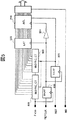
本発明に係る実施の形態について、添付図面を参照しながら以下詳細に説明する。図1は、本発明の実施形態としてのループ利得の変動を抑圧できるループ利得検出回路を備えたPLL回路の基本構成を示す、ブロック図である。
図1において、位相同期ループ(PLL)回路は、第1のループフィルタ100と、この第1のループフィルタの出力が周波数制御端子に接続された第1の電圧制御発振器102と、この第1の電圧制御発振器の出力が接続される第1の周波数変換回路(DCM)107と、第1の位相比較器(PD)101と、この第1の位相比較器101の出力と第1のループフィルタ100の入力の間に接続される第1のチャージポンプ回路(CP)105とを備えている。
Embodiments according to the present invention will be described below in detail with reference to the accompanying drawings. FIG. 1 is a block diagram showing a basic configuration of a PLL circuit including a loop gain detection circuit capable of suppressing fluctuations in loop gain as an embodiment of the present invention.
In FIG. 1, a phase locked loop (PLL) circuit includes a
第1の位相比較器101は、第1の周波数変換回路107の出力が接続された第1の入力(IN−1)と、第1の基準信号(fREF1)112が接続された第2の入力(IN−2)とを備えている。また、第1の位相比較器101の第2の入力(IN−2)には、切り替えスイッチ107を介して、前記第1の基準信号とは別の、ステップ信号(第2の基準信号)を接続できる。第2の入力(IN−2)に接続される第1の基準信号112は、例えばシンセサイザ(高周波発振器)108の出力信号を利用して生成される送信信号である。また、第2の基準信号は、例えばシンセサイザ108の出力信号を基に第1の信号源109から供給されシグマデルタ変調回路111により周波数が変調されたループ特性検出用のステップ信号である。さらに、第2の基準信号を発生する第1の信号源109は、第1の基準信号(fREF1)を発生させる過程で生じる遅延を補償する構成を有する。
The
このPLL回路において、ループ特性検出にあたっては、第1の信号源108から供給される位相比較器101の第2の入力(IN−2)への入力信号の周波数をステップ状に変化させ、その変化に対する応答を電圧制御型発振器102の出力で検出する。検出手段は、例えば、電圧制御型発振器102の出力に接続されたカウンタ103の出力に積分器104を接続することで実現される。
In this PLL circuit, when detecting loop characteristics, the frequency of the input signal to the second input (IN-2) of the
制御部220の演算部において、この積分器104による検出結果に基きチャージポンプ電流値の算出を行い、チャージポンプ105にフィードバックする。
VCOの発振周波数の電圧制御感度をKv、チャージポンプ105の駆動電流をIcp、容量をCとすれば、これらの値とループ利得とは次式の関係にある。
ループ利得∝(Icp・Kv)/C
この関係を利用して、チャージポンプ電流Icpを最適化することで、ループ帯域を校正し、PLL回路の位相同期ループ特性を最適化することができる。
The calculation unit of the
Assuming that the voltage control sensitivity of the oscillation frequency of the VCO is Kv, the drive current of the
Loop gain ∝ (Icp · Kv) / C
By utilizing this relationship, the charge pump current Icp is optimized, so that the loop band can be calibrated and the phase locked loop characteristic of the PLL circuit can be optimized.
本実施形態では、特に、第2の基準信号を生成する第1の信号源109において、シグマデルタ変調回路111が発生する周波数を、フラクショナル周波数(RFVCOの周波数に対する少数分周比)に設定する構成とすることにより、遅延要素によるバラツキを低減することができる。
In the present embodiment, in particular, in the
本実施形態では、位相比較器101における基準信号入力側(IN−2)に、ループ帯域を検出するための信号を直接入力する。そのため、オフセットPLL送信機を代表とする、チャージポンプ電流を可変とする様々なタイプのPLLに適用することができる。
In this embodiment, a signal for detecting a loop band is directly input to the reference signal input side (IN-2) in the
また、本実施形態によれば、ループ帯域を校正する時間が短いという利点がある。さらに、本来はローカル用に使用する信号を分周器を用いて分周して位相比較器の基準信号側(IN−2)に入力しており、ローカル信号を有効利用できる。 Moreover, according to the present embodiment, there is an advantage that the time for calibrating the loop band is short. Furthermore, the signal originally used for local use is frequency-divided by using a frequency divider and inputted to the reference signal side (IN-2) of the phase comparator, so that the local signal can be used effectively.
本実施形態の校正回路は、ステップ応答検出に必要なカウンタ103、積分器104等を全てデジタル回路で構成することが可能であり、PLL回路への集積化が可能である。
In the calibration circuit of the present embodiment, the
また、位相雑音が少なく負荷変動の影響を受けにくい、位相同期ループ回路を実現することができる。また、PLL回路のアナログ特性は、誤差フィードバック量、発振器の制御感度、ループフィルタの特性などで決まるが、本実施例の校正回路によれば、これらのすべて性能バラツキを、高い校正精度で、一括校正することが可能である。これにより、ループフィルタ回路の全体をPLL回路に集積化し、高周波アナログLSIの小型、高性能化を実現することができる。 Further, it is possible to realize a phase-locked loop circuit that has little phase noise and is not easily affected by load fluctuations. The analog characteristics of the PLL circuit are determined by the amount of error feedback, the control sensitivity of the oscillator, the characteristics of the loop filter, etc., but according to the calibration circuit of this embodiment, all these performance variations can be achieved with high calibration accuracy. It is possible to calibrate. As a result, the entire loop filter circuit can be integrated in the PLL circuit, and the high-frequency analog LSI can be reduced in size and performance.
なお、積分器104の出力に更に積分器を多段に接続すれば、検出精度の向上を図ることができる。 It should be noted that if more integrators are connected to the output of the integrator 104 in multiple stages, detection accuracy can be improved.
本発明のより具体的な実施の形態について、添付図面を参照しながら以下詳細に説明する。 More specific embodiments of the present invention will be described below in detail with reference to the accompanying drawings.
本発明の第1の実施例について図2から図7を用いて説明する。本実施例は、オフセットPLL型の位相同期ループ回路に、ステップ波形を入力し、その応答を電圧制御型発振器201の出力で検出するというものである。
A first embodiment of the present invention will be described with reference to FIGS. This embodiment, the offset PLL type phase locked loop circuit, by entering the waveform, is that for detecting the response at the output of the voltage-controlled
まず、図2で、本発明の第1の実施例になるオフセットPLL型位相同期ループ回路およびそれを含むオフセットPLL送信機の全体の構成及び動作を説明する。
最初に、オフセットPLLの構成及び動作の原理について簡単に説明する。オフセットPLL型の位相同期ループ回路は、電圧制御型発振器(VCO)201とダウンコンバージョンミキサ(DCM)202と位相比較器(PD)203とチャージポンプ(CP)204とループフィルタ(LF)205とで構成されている。
First, the overall configuration and operation of an offset PLL type phase locked loop circuit and an offset PLL transmitter including the same will be described with reference to FIG.
First, the configuration and operation principle of the offset PLL will be briefly described. The offset PLL type phase-locked loop circuit includes a voltage controlled oscillator (VCO) 201, a down-conversion mixer (DCM) 202, a phase comparator (PD) 203, a charge pump (CP) 204, and a loop filter (LF) 205. It is configured.
このPLL回路の位相比較器203の第1の入力(IN−1)に、スイッチ221を介してVCO201の出力が入力される。このVCO201の出力は、スイッチ216を介して位相比較器203の第2の入力(IN−2)に入力された第1の基準信号(fREF1)と比較され、比較の結果得られた位相誤差に基づいて、パルス幅が決定される。そして、このパルス幅の電流をチャージポンプ204より出力し、ループフィルタ205で積分した後、VCO201の周波数制御端子に帰還する。このようにして、PLL回路は、位相比較器203における第1の入力(IN−1)と第2の入力(IN−2)の位相誤差が最小になる状態に収束する。
The output of the
この位相同期ループ回路において、送信モード時には直交変調器206からの送信信号(fREF1)を、位相比較器203の第2の入力(IN−2)に基準信号として入力することで電圧制御型発振器201の出力に変調信号が発生する。フラクショナル型のシンセサイザ207を用いる場合は、直交変調器206へ入力するローカル信号と、ダウンコンバージョンミキサ(DCM)202へ入力するローカル信号を同一のシンセサイザ207から生成することが可能である。この場合、一例として、直交変調器206へのローカル信号には、シンセサイザ207の出力信号を、分周器208を用いて10から13の値で分周を行い、更に90度シフタ209を通した信号を用いる。このときに、ダウンコンバージョンミキサ(DCM)202へのローカル信号には、シンセサイザ207の出力信号を分周器210で2分周または4分周した信号を用いる。
In this phase-locked loop circuit, in the transmission mode, the transmission signal (fREF1) from the
なお、シンセサイザ207の基準信号のクロック信号を生成するために、電圧制御型水晶発振器(VCXO)240が設けられている。この電圧制御型水晶発振器240は、水晶発振器242と同調して、基準信号を生成する。
Note that a voltage controlled crystal oscillator (VCXO) 240 is provided in order to generate a clock signal as a reference signal of the
次に、ループ特性検出に用いるステップ波形の生成装置及び生成方法について説明する。まず、ステップ波形の生成装置は、シンセサイザ207の出力信号を分周する分周器211と、その分周数を制御するシグマデルタ変調回路232で構成されている。分周器211は、分周器212、分周器213、および分周器214を有し、その出力信号は、ローパスフィルタ215及びスイッチ216を介して位相比較器203の第2の入力(IN−2)に送られる。
Next, a step waveform generation apparatus and generation method used for loop characteristic detection will be described. First, the step waveform generation apparatus includes a
分周器211では、まずシンセサイザ207の出力信号を分周器212で4分周して、その出力を分周器213で10から13分周数する。この10から13分周器をシグマデルタ変調器232で制御し、フラクショナル動作させる。その出力を分周器214で2分周する。分周器211の構成はこの例に限定されるものではない。
In the
なお、分周器211の分周器214の出力信号をシグマデルタ変調器232のクロックとして使用すれば、分周器211とシグマデルタ変調器232の同期がとれるため、都合が良い。
Note that it is convenient to use the output signal of the
位相比較器203の第1の入力(IN−1)側にあるスイッチ221には、ダウンコンバージョンミキサ(DCM)202の出力が直接供給される第1のパスと、2分周器219及びローパスフィルタ222を経由する第2のパスとが接続されている。スイッチ221は、位相同期ループ回路の動作状態、すなわち通常モードあるいはループ特性検出モードに応じて、切り替えられる。
The
また、位相比較器203の第2の入力(IN−2)側にあるスイッチ216も、位相同期ループ回路の動作状態、すなわち通常の通信モードあるいはループ特性検出モードに応じて動作し、直交変調器206からの送信信号もしくはローパスフィルタ215からのループ特性検出用信号のいずれかを選択する。
The
次に、ループ特性検出用ステップ信号について説明する。分周器211の出力信号は、ローパスフィルタ215で波形を整えた後に、スイッチ216を介して位相比較器203の第2の入力(IN−2)に入力される。ループ特性検出モードのとき、スイッチ216は、ローパスフィルタ215側のループ特性検出用信号を選択する。
Next, the loop characteristic detection step signal will be described. The output signal of the
このとき、位相比較器203の第1の入力(IN1)に対応する入力スイッチ221では、2分周器219を経由する第2のパスを使用する。これは、ループ特性検出モードにおいて、シグマデルタ変調器232の動作クロックを抑えるために、通常モードの1/2の周波数を位相比較器203の入力信号として用いるためである。
At this time, the
ループ特性検出用のステップ信号は、シグマデルタ変調器232で分周器211の分周数を変化させることで行う。シグマデルタ変調器を用いることで、ループ特性検出に適した任意の微小な周波数ステップ信号を容易に生成することが可能である。
The step signal for loop characteristic detection is performed by changing the frequency division number of the
次に、ループ特性検出モード時に、第1の基準信号すなわち直交変調器206からの送信信号(fREF1)を発生させる過程で生じる遅延を補償する構成について説明する。本実施例の位相同期ループ回路において、ループ特性検出のためのオフセットPLL中のステップ信号は、シグマデルタ変調器232で分周器211の分周数を変化させることで行っている。この場合、分周器211の分周比をフラクショナル値からフラクョナル値へステップさせる。すなわち、本実施例では、ループ特性検出モード時に分周器211が、フラクショナル値からフラクョナル値へステップするように制御することで、第1の基準信号(fREF1)を発生させる過程で生じる遅延を補償している。
Next, a configuration for compensating for a delay generated in the process of generating the first reference signal, that is, the transmission signal (fREF1) from the
次に、ループ特性の検出装置について説明する。ループ特性を検出する装置としては、電圧制御型発振器201の出力にカウンタ217を設け、その出力に積分器218を接続する。カウンタ217のカウント値をサンプリングするクロックとしては、ダウンコンバージョンミキサ202の出力を分周器219で2分周した信号を用いると、安定した精度が得られる。検出した結果は、制御部220の演算部で線形近似による簡単な計算処理を得て、チャージポンプ204の電流値が最適になるように、反映される。この制御部の詳細については、後で説明を記載する。
Next, a loop characteristic detection device will be described. As an apparatus for detecting the loop characteristics, a
次に、位相同期ループ回路のループ特性を検出するシーケンスを、図3と図4(図4A、図4B)を用いて説明する。 Next, a sequence for detecting the loop characteristics of the phase-locked loop circuit will be described with reference to FIGS. 3 and 4 (FIGS. 4A and 4B).
まず、図2のシステムの各部における動作波形を図3に記す。波形301は、シグマデルタ変調器232に入力されるステップ信号で、例えば通常動作で11分周を使いたい場合は、10.9分周から11.1分周といった11分周付近でのフラクショナルなステップ信号を入力する。波形302は、電圧制御型電圧源201の出力での周波数変化の様子である。波形301のステップ信号が、オフセットPLLがロックしている状態で、位相比較器203に入力されると、波形302で見られるように、ループ利得が適正値よりも高い場合には、電圧制御型電圧源201の出力における周波数変化は早く、ループ利得が適正値よりも低い場合には、周波数変化は遅くなる。
First, FIG. 3 shows operation waveforms in each part of the system of FIG. A waveform 301 is a step signal input to the
波形303は、オフセットPLLがロックしている状態でのカウンタ217の出力の様子である。波形304は、ステップ応答におけるカウンタ出力の様子で、ステップ波形が入力された瞬間にカウント値ゼロから再開される。ループ利得が適正値よりも高い場合と低い場合で、カウント値の差異が見られるが、その差異は、微小である。
A waveform 303 shows an output state of the
波形305は、カウント値をサンプリングするためのクロックで、この場合、分周器219の出力信号が用いられる。このクロックでサンプリングされたカウント値は、後段の積分器218で積分される。波形306は、積分器218の積分値で、オフセットPLLがロックしている状態での変化である。波形307は、同じく積分器218の積分値で、ステップ応答における積分値の変化である。ループ利得が高い場合と低い場合で、積分値は異なり、その差異は、カウンタ217での差異と比較して、大きい。すなわち、積分することでより高精度に差異を検出できる。
A waveform 305 is a clock for sampling the count value. In this case, an output signal of the
波形307の終端Bと、波形306の終端Aの値の差(B-A)は、ループ利得の逆数(1/Loop-gain)に対してほぼ比例関係で変化する。この比例関係を制御部220の演算で利用している。
The difference (B−A) between the values of the end B of the
次に、図4A、図4Bを使って、実施例1におけるループ特性検出モード時の動作シーケンスを説明する。図4Aはループ特性検出処理のフローチャート、図4Bはループ特性検出処理のタイムチャート及びそれに対応する電圧制御型発振器(VCO)201の周波数特性を示す図である。 Next, an operation sequence in the loop characteristic detection mode according to the first embodiment will be described with reference to FIGS. 4A and 4B. FIG. 4A is a flowchart of the loop characteristic detection process, and FIG. 4B is a time chart of the loop characteristic detection process and a frequency characteristic of the voltage controlled oscillator (VCO) 201 corresponding thereto.
まず、シンセサイザ207をロック状態にする(401)。次に、VCO201にプリチャージを行った後、time=t1でオフセットPLLをロック状態(周波数f1)にする(402)。このとき、位相比較器203の第2の入力(IN2)に対応するスイッチ216と位相比較器203の第1の入力(IN1)に対応するスイッチ221は、共にループ特性を検出する検出モードである。
First, the
この状態(t2)で、図3の波形306における終端Aの値を測定し(403)、レジスターに保持する(t3)。次に(t4)、シグマデルタ変調器232からステップ信号(周波数f2)を入力する(404)。このときのステップ応答を図3の波形307の終端Bで測定する(405)。次に(t5)、波形306の終端Aの値との差(B-A)を計算する(406)。制御部220で、チャージポンプ電流値の算出を行い、チャージポンプ204の値へフィードバックし(407)、送信周波数ftxの前後で帯域制御を行ない、オフセットPLLをロック状態にする(t6)。これにより、ループ特性検出のためのキャリプレーションが完了し、通常の通信モードに移行する(t7)。
In this state (t2), the value of the terminal A in the
次に、図5を用いて、本実施例のカウンタ回路217及びアキュムレータ回路218の構成の詳細について説明する。カウンタ回路217は、VCOの信号(fVCO)で駆動される8ビット同期カウンタ(8bSYNC_CT)501と、このカウンタの出力で駆動される8ビット同期カウンタ(8bSYNC_CT)502で構成される。カウント経過を基準クロックREFCLKの周期でラッチ(LAT)503に取りこみ、インバータ504で反転させたクロックでアキュムレータ(ACL)回路218に取りこむ。ラッチ503の取り込みタイミングと、VCO201のカウントタイミングの衝突を防止するため、ラッチ503を駆動する前に、基準クロックをVCO信号でDラッチ回路(D−LAT)505をたたくことで、タイミングを合わせる。カウント開始はリセット信号(RST)の解除によって開始されるが、これも同様に、Dラッチ回路506を基準クロック、VCO信号との衝突を防止するため、基準クロック、VCO信号でたたきなおすことでタイミングを合わせる。データ読出し信号(RD)は、例えば、High状態でラッチ回路503をアクティブにし、アキュムレータ218の出力を比較演算部に出力する。
Next, details of the configuration of the
次に、図2の制御部220の構成及び作用の詳細について図6を使って説明する。制御部220では、図3に示す波形307の終端Bと、波形306の終端Aの値との差(B-A)が、ループ利得の逆数(1/Loop-gain)に対してほぼ比例関係で変化するという事実を利用した演算処理を行う。波形306における終端Aの積分結果(601)と、波形307における終端Bの積分結果(602)を、まず引き算し(B-A)、検出用に使うステップ信号が、ステップアップ/ダウン信号かにより極性を変える(603)。この結果から、設定したいループ帯域に応じた、基準値604を引き、係数605を掛ける。基準値604と係数605に対しては、位相同期ループの出力周波数により依存性があるため、出力周波数により値が変化するようにレジスタを用意する。この演算結果606は、検出時のループ利得に対して、どの割合でループ利得を変化させれば最適なループ利得かを示す値である。この演算結果606を、検出時に用いたチャージポンプ電流値607に掛けることで、最適なループ帯域にするためのチャージポンプ電流値(Icp)608を決定する。
Next, details of the configuration and operation of the
図7は、図2の可変電流型のチャージポンプ(CP)の具体例を示す図である。チャージ電流源701を並列につなぎ、幾つ動作させるかにより、チャージ電流値を決定する。また、ディスチャージ電流源702も同様に並列につなぎ、同様に幾つの電流源を動作させるかで、ディスチャージ電流値を決定する。これらの電流源を幾つ動作させるかを、チャージポンプ電流値(Icp)608により決定する。
FIG. 7 is a diagram showing a specific example of the variable current type charge pump (CP) of FIG. The charge current value is determined depending on how many charge
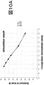
図8に、図2の実施例に基づく、ループ特性検出のシミュレーション結果を示す。縦軸はB-Aの値で、横軸はループ利得の逆数で、値は設計値により規格化されている。図中、ループ利得の逆数が1.0のときが最適値である。この図より、B-Aの値は、ループ利得の逆数に対し、ほぼ線形であることがわかる。 FIG. 8 shows a simulation result of loop characteristic detection based on the embodiment of FIG. The vertical axis is the B-A value, the horizontal axis is the reciprocal of the loop gain, and the value is normalized by the design value. In the figure, the optimum value is when the reciprocal of the loop gain is 1.0. From this figure, it can be seen that the value of B-A is substantially linear with respect to the reciprocal of the loop gain.
ここで、第1の基準信号すなわち直交変調器206からの送信信号(fREF1)を発生させる過程で生じる遅延を補償するために、ループ特性検出モード時に、クショナル値からフラクョナル値へステップするように制御することの効果を、オフセットPLL中に遅延が生じた場合のシミュレーションの結果として、図9(図9A、図9B)及び図10(図10A、図10B)で説明する。
Here, in order to compensate for a delay generated in the process of generating the first reference signal, that is, the transmission signal (fREF1) from the
まず、図9A、図9Bは、比較のための例であり、シミュレーションの条件として、ステップ信号生成用の分周器211がインテジャ値(整数値)からフラクショナル値へステップした場合の例である。図9Aはループ利得の逆数とB-Aの値の関係、図9Bはループ利得の逆数とループ帯域を検出できる精度の関係を示している。図9A、図9Bの各3本の特性曲線のうち、中央の菱形印の特性曲線は遅延の無い状態、丸印の特性曲線は450Psの遅延が有り、角印の特性曲線は500Psの遅延が有る例である。図9Bから明らかなように、遅延に対して感度があり、ループ帯域を検出できる精度が+/-20%を上回る場合もある。
First, FIG. 9A and FIG. 9B are examples for comparison, and are examples when the
次に、図10A、図10Bは、本発明の実施例に対応するものであり、シミュレーションの条件として、分周器211がフラクショナル値からフラクョナル値へステップした場合の例である。図10Aはループ利得の逆数とB-Aの値の関係、図10Bはループ利得の逆数とループ帯域を検出できる精度の関係を示している。この場合、電圧制御型信号源201と分周器219出力の積分用クロックにおいて、初期位相の関係が、測定403と測定404で同じ初期位相で測定できるため、遅延に対する感度を打ち消すことができる。
Next, FIG. 10A and FIG. 10B correspond to the embodiment of the present invention, and are examples when the
図10A、図10Bの各3本の特性曲線のうち、中央の菱形印の特性曲線は遅延の無い状態、丸印の特性曲線は250Psの遅延が有り、角印の特性曲線は900Psの遅延が有る例である。図10Bに示すように、この場合のループ帯域を検出できる精度は+/-6%以下であり、図9Bの場合と比較し、精度を大幅に改善できる。 Of the three characteristic curves shown in FIGS. 10A and 10B, the characteristic curve indicated by the rhombus at the center has no delay, the characteristic curve indicated by a circle has a delay of 250 Ps, and the characteristic curve indicated by a square has a delay of 900 Ps. There is an example. As shown in FIG. 10B, the accuracy with which the loop band can be detected in this case is +/− 6% or less, and the accuracy can be greatly improved compared to the case of FIG. 9B.
このように、本実施例によれば、PLL回路のループ利得の測定結果によりチャージポンプ電流を可変できるため、短い時間でかつ高精度に最適のループ帯域を設定できる校正システムを提供できる。特に、シグマデルタ変調器を用いることで、ループ特性検出に適した微小な周波数ステップ信号を容易に生成することが可能である。 As described above, according to the present embodiment, the charge pump current can be varied according to the measurement result of the loop gain of the PLL circuit. Therefore, it is possible to provide a calibration system capable of setting an optimum loop band in a short time and with high accuracy. In particular, by using a sigma delta modulator, it is possible to easily generate a minute frequency step signal suitable for loop characteristic detection.
また、本実施例によれば、ループ利得検出回路を設けることにより、PLL回路のループ利得の測定結果によりチャージポンプ電流を可変できるため、素子の特性ばらつきや、温度や経年変化を打ち消して、常に最適なループ帯域を保つことができる。また、短時間での自動検出が可能であり、人手の作業を必要としない。更に、本発明の検出回路は、全てデジタル回路で構成することができ、高集積化・低消費電力化を図ることができる。また、第1の基準信号すなわち直交変調器206からの送信信号(fREF1)を発生させる過程で生じる遅延を補償することができる。
[変形例1]
なお、図3では、実施例1の位相同期ループ回路における積分器218による積分時間、すなわち波形307での積分値ゼロから終端Bまでの時間T1と、波形306での積分値ゼロから終端Aまでの時間T2が等しいことを前提に説明した。しかし、実施例1の変形例として、積分時間T1と積分時間T2の関係を最適化することで、差分値(B-A)とループ利得の逆数(1/Loop-gain)の比例関係を改善することもできる。
[変形例2]
また、実施例1の位相同期ループ回路では積分器218が一段の構成となっていたが、これに代えて、積分器を多段に接続し、前段の積分器で得られた差分値(B-A)を、後段の積分器で同期してさらに積分するように構成しても良い。このような構成とすることで、差分値(B-A)とループ利得の逆数(1/Loop-gain)の比例関係の特性がより改善され、ループ特性を検出する精度の向上を図ることができる。
In addition, according to the present embodiment, by providing the loop gain detection circuit, the charge pump current can be varied according to the loop gain measurement result of the PLL circuit, so that it is always possible to cancel the element characteristic variation, temperature, and aging. An optimal loop bandwidth can be maintained. In addition, automatic detection in a short time is possible, and no manual work is required. Furthermore, the detection circuit of the present invention can be entirely constituted by a digital circuit, and high integration and low power consumption can be achieved. Further, it is possible to compensate for the delay that occurs in the process of generating the first reference signal, that is, the transmission signal (fREF1) from the
[Modification 1]
In FIG. 3, the integration time by the
[Modification 2]
In the phase-locked loop circuit of the first embodiment, the
また、第1の基準信号を発生させる過程で生じる遅延を補償する手段として、実施例1では、位相同期ループ回路において、シグマデルタ変調器232で分周器211の分周数を変化させたステップ信号を生成することで行っているが、この構成に限定されるものではない。
As a means for compensating for a delay that occurs in the process of generating the first reference signal, in the first embodiment, in the phase-locked loop circuit, the step of changing the frequency division number of the
次に、図11を用いて、本発明の第2の実施例になるオフセットPLL型位相同期ループ回路およびそれを含むオフセットPLL送信機の全体の構成及び動作を説明する。先に述べた第1の実施例では、カウンタ217のカウント値をサンプリングするクロックとしては、ダウンコンバージョンミキサ202の出力を分周器219で2分周した信号を用いていた。積分器218でサンプリングに使用するクロックとしてはこれに限定されるものではない。
Next, the overall configuration and operation of an offset PLL type phase locked loop circuit and an offset PLL transmitter including the same according to a second embodiment of the present invention will be described with reference to FIG. In the first embodiment described above, as the clock for sampling the count value of the
第2の実施例では、積分器218のクロックとして、分周器208の出力信号を分周器1001でさらに8分周した信号を使用する。この場合には、ステップ信号を入力するタイミングと、分周器208の遅延が常に同じ関係になるようにするため、分周器208と分周器1001に対して初期値を設定する必要がある。
In the second embodiment, a signal obtained by further dividing the output signal of the
本実施例によれば、PLL回路のループ利得の測定結果によりチャージポンプ電流を可変できるため、短い時間でかつ高精度に最適のループ帯域を設定できる校正システムを提供できる。 According to the present embodiment, since the charge pump current can be varied according to the loop gain measurement result of the PLL circuit, it is possible to provide a calibration system capable of setting an optimum loop band in a short time and with high accuracy.
次に、本発明の第3の実施例を説明する。図12により、図2等で述べた実施形態になる位相同期ループ回路を、マルチバンド方式の移動体通信システム(携帯電話)を構成する高周波LSIに適用した場合について説明する。図12の通信システムは、高周波集積回路部1100と、ベースバンド信号処理を行うLSI部1102とパワーアンプ(PA)部1104とアンテナ部1110と基準信号を生成するクリスタル部1105で構成されている。
Next, a third embodiment of the present invention will be described. The case where the phase-locked loop circuit according to the embodiment described in FIG. 2 and the like is applied to a high-frequency LSI constituting a multiband mobile communication system (mobile phone) will be described with reference to FIG. The communication system in FIG. 12 includes a high-frequency
高周波集積回路部1100は、送信系回路(Transmitter)1101、LSI部1102で生成された信号をDA変換し送信系回路(Transmitter)1101へ送るDAコンバータ1103、シンセサイザブロック1207、及び90度シフタ1209を備えている。
The high-frequency
また、受信系回路として、受信信号を増幅するロウノイズアンプ(Low-noise Amplifier:LNA)1112、受信信号の復調を行なう復調回路、復調された信号をAD変換してベースバンドLSIへ出力するADコンバータ1113等が設けられている。
In addition, as a reception system circuit, a low-noise amplifier (LNA) 1112 that amplifies the reception signal, a demodulation circuit that demodulates the reception signal, and AD that converts the demodulated signal to AD and outputs it to the baseband
なお、図12の二点鎖線で囲まれた領域の送信系回路(Transmitter)1101、シンセサイザブロック1207及び90度シフタ1209は、図2や図11のオフセットPLL送信機に対応するものである。前に述べた実施例と異なり、シンセサイザブロック1207と90度シフタ1209は、送信系回路のみならず受信系回路のローカル信号の生成にも関与している。
Note that the transmission system circuit (Transmitter) 1101, the
この実施例においては、シンセサイザブロック1207等二点鎖線で囲まれた領域には、図2や図11に示されているような構成を有する回路が使用されており、チャージポンプ電流を最適化することにより、ループ帯域を校正する。
In this embodiment, a circuit having a configuration as shown in FIG. 2 or FIG. 11 is used in a region surrounded by a two-dot chain line such as the
ループ帯域の校正にあたっては、まず、シンセサイザ1207に基準信号を供給するクリスタル部1105からの信号1106をステップ変化させる。このステップ変化した信号は、シンセサイザ部1207の位相比較器の基準信号側に入力される。このステップ信号をシンセサイザにおける出力信号1107において、カウンタと積分器を用いて検出する。
In calibrating the loop band, first, the
このことで、シンセサイザブロック1207は、常に最適なループ帯域に設定され、送信用のローカル信号1108と受信用のローカル信号1109を安定に供給することができる。この実施例を用いることで、送信と受信におけるローカル信号の雑音レベルを一定に保つことが可能である。
Thus, the
また、本実施例の移動体通信システムは、シンセサイザ1207にループ帯域の校正システムを有するオフセットPLL送信機を採用することで、ループ帯域を校正する時間を短くできる。特に、オフセットPLL中のステップ信号の生成にシグマデルタ変調器を用いることで、ループ特性検出に適した微小な周波数ステップ信号を生成することが容易である。
In the mobile communication system of the present embodiment, the time required to calibrate the loop band can be shortened by adopting an offset PLL transmitter having a loop band calibration system for the
本実施例によれば、校正回路をステップ応答検出に必要なカウンタ、積分器を全てデジタル回路で構成することが可能である。また、PLL回路のアナログ特性は、誤差フィードバック量、発振器の制御感度、ループフィルタの特性などで決まるが、本実施例の校正回路は、これらのすべて性能バラツキを、高い校正精度で、一括校正することが可能である。これにより、ループフィルタ回路全体をPLL回路に集積化し、高周波アナログLSIの小型、高性能化を実現することができる。これらにより、ループ帯域の校正システムを有するシンセサイザブロック207を備えた高周波集積回路部1101を実現することができる。しかも、位相雑音が少なく負荷変動の影響を受けにくい、位相同期ループ回路を実現することができる。
According to the present embodiment, it is possible to configure the calibration circuit as a counter necessary for step response detection and the integrator as a digital circuit. The analog characteristics of the PLL circuit are determined by the amount of error feedback, the control sensitivity of the oscillator, the characteristics of the loop filter, etc., but the calibration circuit of this embodiment calibrates all of these performance variations with high calibration accuracy. It is possible. As a result, the entire loop filter circuit can be integrated into the PLL circuit, and the high-frequency analog LSI can be reduced in size and performance. Thus, the high-frequency
また、本発明では、位相比較器における基準信号入力側にループ帯域を検出するための信号を直接入力する方式なので、オフセットPLL送信機を代表とする、様々な方式のPLLに適用することができる。 In the present invention, since a signal for detecting a loop band is directly input to the reference signal input side of the phase comparator, the present invention can be applied to various types of PLLs represented by an offset PLL transmitter. .
次に、図13を用いて本発明の第4の実施例を説明する。
図13は、図12の高周波集積回路部1100を半導体集積回路チップ1300として構成した場合のレイアウトの一例を示すものである。
この半導体集積回路チップ1300は、平面形状が実質的に矩形、より好ましくは正方形のチップである。図13の集積回路チップ1300には、図12の二点鎖線で囲まれた領域の送信系回路(Transmitter)1101、シンセサイザブロック1207及び90度シフタ1209の部分を表示し、他の部分の表示は省略している。
Next, a fourth embodiment of the present invention will be described with reference to FIG.
FIG. 13 shows an example of a layout when the high-frequency
The semiconductor integrated circuit chip 1300 is a chip having a substantially rectangular planar shape, more preferably a square. The integrated circuit chip 1300 in FIG. 13 displays the transmission system circuit (Transmitter) 1101, the
まず、送信系回路1101内の発振器(VCO)201とダウンコンバージョン用のミキサ(DCM)202との間に、校正用のカウンタ217とアキュムレータ218と制御部220とを配置する。このとき、発振器201は、周囲へのカップリングの影響を避けるために集積回路チップの角(第1の角)に位置させ、また、ダウンコンバージョンミキサ202は、発振器201からのカップリングの影響を避けるために、集積回路チップの別の角(第2の角)、例えば同じ辺上の他の角に位置させる。カウンタ217とアキュムレータ218および制御部220については、デジタル素子であり、離散動作を行うため、発振器201からのアナログ要因のカップリングを受けにくい。そこで、発振器201とダウンコンバージョンミキサ202の間に、カウンタ217とアキュムレータ218と制御部220を位置させると良い。そして、これらのデジタル素子(カウンタ217とアキュムレータ218および制御部220)とダウンコンバージョンミキサ202との間に、例えば矩形の下辺の近傍に、位相比較器203、チャージポンプ204及び直交変調部206、スイッチ類(216、221)を配置する。このことで、発振器201の周囲に、特にガードを生成することなく、送信機における低雑音化を実現できる。また、ガードを必要としない分、チップ面積の削減が可能である。
First, a
次に、ローカル信号を生成するシンセサイザ(発振器)1207は、発振器201との干渉を避けるために、発振器201から遠くに位置させる。例えば、図に示したように、前記第1の角と第2の角を矩形の下辺の両端としたとき、発振器1207は、第1、第2の角を含まない辺、すなわち矩形の上辺の近傍に配置する。分周器208、4分周器と90度位相シフタ209、分周器211、90度シフタ1209などは、シンセサイザ1207の近傍に配置される。なお、シンセサイザ1207から直交変調部206とダウンコンバージョンミキサ202への距離については、なるべく近くなるように配置すると良い。すなわち、シンセサイザ1207、矩形の上辺の中間付近もしくはこれよりやや左寄りに配置すると良い。このことで、配線におけるジッターやカップリングの影響を軽減することが可能であり、ローカル信号の雑音を抑えることができる。
Next, a synthesizer (oscillator) 1207 that generates a local signal is positioned far from the
さらに、電圧制御型水晶発振器(VCXO)1301は、外付けのクリスタル部(水晶発振器)1105と同調して、チップ内の基準信号を生成し、また、電圧制御により周波数誤差を校正する役割を果たす。特に、電圧制御型水晶発振器1301は、シンセサイザ1207の基準信号や図12におけるLSI部1102内のロジックのクロック信号を生成するために、雑音やカソプリングの影響を十分に考慮する必要がある。このため、電圧制御型水晶発振器1301は、第1、第2の角から離れたチップの角、例えば矩形の上辺の角(第3の角)に配置すると良く、これにより、ロジックにおけるクロック信号のジッター雑音の抑圧と、発振器207における位相雑音の抑圧を実現することが可能である。
Further, the voltage controlled crystal oscillator (VCXO) 1301 is synchronized with an external crystal unit (crystal oscillator) 1105 to generate a reference signal in the chip, and also serves to calibrate a frequency error by voltage control. . In particular, the voltage-controlled
なお、高周波集積回路部1100の他の構成要素に関しては、上記したレイアウトに沿い、集積回路チップ1300内の残りの領域に適宜配置される。
The other components of the high-frequency
本実施例によれば、様々なタイプの位相同期ループにおけるループ帯域を、簡単な構成で高精度に設定でき、PLL回路に集積化して高集積化・低消費電力化を図ることができると共に、低雑音でかつチップ面積を削減できる通信用高周波集積回路を提供することができる。 According to the present embodiment, the loop band in various types of phase-locked loops can be set with high accuracy with a simple configuration, and can be integrated in a PLL circuit to achieve high integration and low power consumption. It is possible to provide a high frequency integrated circuit for communication that can reduce the chip area with low noise.
PLL…位相同期ループ、VCO…電圧制御型信号源、CP…チャージポンプ、PD…位相比較器、Ctrl.…チャージポンプ制御部、SD…シグマデルタ変調器、Div.…分周器、LPF…ローパスフィルタ、synth…シンセサイザ、DCM…ダウンコンバージョンミキサ、slot…スロット、cal.…校正(キャリブレーション)、Icp…チャージポンプ電流、ACC…積分(アキュムレート)、A…1回目の測定結果、B…2回目の測定結果、freq.…周波数、101…位相比較器、102…電圧制御型信号源、103…カウンタ、104…積分器(アキュムレータ)、105…チャージポンプ、201…電圧制御型信号源、202…ダウンコンバージョンミキサ、203…位相比較器、204…チャージポンプ、205…ループフィルタ、206…直交変調器、207…シンセサイザ、208…10〜13分周器、209…4分周器と90度位相シフタ、210…4または2分周器、211…分周器、212…4分周器、213…10〜13分周器、214…2分周器、215…ローパスフィルタ、216…スイッチ、217…カウンタ、218…積分器(アキュムレータ)、219…2分周器、220…チャージポンプ電流制御部、221…スイッチ、232…シグマデルタ変調器、240…電圧制御型水晶発振器、242…水晶発振器、301…シグマデルタ入力での波形、302…VCO出力での波形、303…カウンタ出力での波形、304…ステップ信号入力中のカウンタ出力での波形、305…サンプル用クロック(積分器用クロック)、306…積分器出力での波形、307…ステップ信号入力中での積分器出力での波形、401…シンセサイザのロックアップまでの遷移状態、402…オフセットPLLでのロックアップまでの遷移状態、403…1回目の測定、404…ステップ信号の入力、405…2回目の測定、406…2回目の測定結果から1回目の測定結果の引き算、407…チャージポンプ電流の設定、601…1回目の測定結果、602…2回目の測定結果、603…ステップアップ信号またはステップダウン信号の選択、604…基準とする値、605…係数(傾き)、606…乗算結果、607…校正中のチャージポンプ電流値、608…最適なチャージポンプ電流値、701…チャージ用回路、702…ディチャージ用回路、1001…8分周器、1100…高周波集積回路部、1101…送信系回路(Transmitter)、1102…ベースバンドLSI部、1103…DAコンバータ、1104…パワーアンプ部、1105…クリスタル部、1106…基準信号、1107…シンセサイザ出力信号、1108…送信系ローカル信号、1109…受信系ローカル信号、1110…アンテナ部、1112…ロウノイズアンプ(Low-noise Amplifier:LNA)、1113…ADコンバータ、1207…シンセサイザブロック、1209…90度シフタ、1300…集積回路チップ、1301…電圧制御型水晶発振器。
PLL ... Phase-locked loop, VCO ... Voltage control type signal source, CP ... Charge pump, PD ... Phase comparator, Ctrl .... Charge pump controller, SD ... Sigma delta modulator, Div .... Divider, LPF ... Low pass Filter, synth ... synthesizer, DCM ... down-conversion mixer, slot ... slot, cal .... calibration (calibration), Icp ... charge pump current, ACC ... integration (accumulate), A ... first measurement result, B ... 2 First measurement result, freq .... frequency, 101 ... phase comparator, 102 ... voltage controlled signal source, 103 ... counter, 104 ... integrator (accumulator), 105 ... charge pump, 201 ... voltage controlled signal source, 202 ... down-conversion mixer, 203 ... phase comparator, 204 ... charge pump, 205 ... loop filter, 206 ... quadrature modulator, 207 ... synthesizer, 208 ... 1 -13 frequency divider, 209 ... 4 frequency divider and 90 degree phase shifter, 210 ... 4 or 2 frequency divider, 211 ... frequency divider, 212 ... 4 frequency divider, 213 ... 10-13 frequency divider, 214 ... 2 frequency divider, 215 ... low pass filter, 216 ... switch, 217 ... counter, 218 ... integrator (accumulator), 219 ... 2 frequency divider, 220 ... charge pump current controller, 221 ... switch, 232 ... sigma delta Modulator, 240 ... Voltage controlled crystal oscillator, 242 ... Crystal oscillator, 301 ... Waveform at sigma delta input, 302 ... Waveform at VCO output, 303 ... Waveform at counter output, 304 ... Counter output during step signal input 305: Sample clock (integrator clock), 306: Waveform at the integrator output, 307: Waveform at the integrator output during step signal input, 40 ... Transition state until lock-up of synthesizer, 402 ... Transition state until lock-up at offset PLL, 403 ... First measurement, 404 ... Step signal input, 405 ... Second measurement, 406 ... Second measurement Subtraction of the first measurement result from the result, 407 ... setting of the charge pump current, 601 ... first measurement result, 602 ... second measurement result, 603 ... selection of step up signal or step down signal, 604 ... with
Claims (32)
前記第1の電圧制御発振器の出力が接続される第1の周波数変換回路と、
前記第1の周波数変換回路の出力が第1の入力に接続され、第2の入力に第1の基準信号が接続される第1の位相比較器と、
前記第1の位相比較器の出力が接続される第1のチャージポンプ回路と、
前記第1のチャージポンプ回路の出力が接続される第1のループフィルタとを具備し、
前記第1のループフィルタの出力が前記第1の電圧制御発振器の入力に接続されて成り、
前記第1の位相比較器の前記第2の入力に、第1の基準信号と周波数が変化するループ特性検出用の第1の信号源とを選択的に接続可能に構成され、
前記第1の信号源は、前記第1のチャージポンプ回路の電流を可変とすることにより、前記第1の基準信号を発生させる過程で生じる遅延を補償する構成を有することを特徴とする位相同期ループ回路。 A first voltage controlled oscillator;
A first frequency conversion circuit to which an output of the first voltage controlled oscillator is connected;
A first phase comparator in which an output of the first frequency conversion circuit is connected to a first input, and a first reference signal is connected to a second input;
A first charge pump circuit to which an output of the first phase comparator is connected;
A first loop filter to which an output of the first charge pump circuit is connected;
The output of the first loop filter is connected to the input of the first voltage controlled oscillator;
The second input of the first phase comparator is configured to be selectively connectable with a first reference signal and a first signal source for detecting loop characteristics whose frequency changes,
The first signal source has a configuration that compensates for a delay generated in the process of generating the first reference signal by making the current of the first charge pump circuit variable. Loop circuit.
前記第1の電圧制御発振器の出力に接続された第1のカウンタと、
前記第1のカウンタの出力に接続された第1の積分器と、
前記第1の積分器の検出結果に基いてループ特性を検出する制御部とを有することを特徴とする位相同期ループ回路。 In claim 1,
A first counter connected to the output of the first voltage-controlled oscillation unit,
A first integrator connected to the output of the first counter;
And a control unit that detects a loop characteristic based on a detection result of the first integrator.
前記周波数が変化する第1の信号源は、前記周波数をフラクショナル周波数に設定し得るものであることを特徴とする位相同期ループ回路。 In claim 1,
The phase-locked loop circuit according to claim 1, wherein the first signal source that changes the frequency can set the frequency to a fractional frequency.
前記周波数が変化する第1の信号源は、第1のシグマデルタ変調器を含むことを特徴とする位相同期ループ回路。 In claim 1,
The phase-locked loop circuit according to claim 1, wherein the first signal source whose frequency changes includes a first sigma-delta modulator.
前記第1の位相比較器の前記第1の入力側に設けられた第1のスイッチと、前記第2の入力側に設けられた第2のスイッチとを備え、
前記第1のスイッチは、前記位相同期ループ回路の動作状態応じて、前記第1の入力を、前記第1の周波数変換回路の出力に直接的に接続された第1のパスと、前記第1の周波数変換回路の出力が分周器を経由して接続された第2のパスのいずれかに切替えられるように構成され、
前記第2のスイッチは、前記位相同期ループ回路の動作状態応じて、前記第2の入力を、前記第1の基準信号もしくは前記周波数が変化する第1の信号源のいずれかに切替えられるように構成されていることを特徴とする位相同期ループ回路。 In claim 1,
A first switch provided on the first input side of the first phase comparator; and a second switch provided on the second input side;
The first switch includes a first path in which the first input is directly connected to an output of the first frequency conversion circuit according to an operation state of the phase-locked loop circuit, and the first switch The output of the frequency conversion circuit is switched to one of the second paths connected via a frequency divider,
The second switch is configured to switch the second input to either the first reference signal or the first signal source whose frequency changes according to an operation state of the phase-locked loop circuit. A phase-locked loop circuit comprising:
前記第1の積分器を複数段の積分器で構成したことを特徴とする位相同期ループ回路。 In claim 2,
A phase-locked loop circuit, wherein the first integrator is composed of a plurality of stages of integrators.
前記第1の積分回路で用いるクロックとして、前記第1の位相比較器の第1の入力側の入力信号を用いることを特徴とする位相同期ループ回路。 In claim 2,
An input signal on a first input side of the first phase comparator is used as a clock used in the first integration circuit.
前記第1の基準信号を生成するためのローカル信号と、前記第1の周波数変換回路へ入力するローカル信号とを、フラクショナル型の発振器からなる同一の高周波発振器で生成することを特徴とする位相同期ループ回路。 In claim 5,
Wherein the local signal for generating said first reference signal and a local signal to be input to the first frequency converting circuit, to generate the same high frequency Oscillator consisting fractional type Oscillator A phase-locked loop circuit.
前記第1の信号源の分周器の出力信号を、前記シグマデルタ変調器のクロックとして使用することを特徴とする位相同期ループ回路。 In claim 4,
An output signal of a frequency divider of the first signal source is used as a clock of the sigma delta modulator.
前記第1の位相比較器の前記第1の入力側に設けられた第1のスイッチと、前記第2の入力側に設けられた第2のスイッチとを備え、
ループ特性検出モードにおいて、前記第1のスイッチは、前記第1の周波数変換回路の出力が2分周器を経由して接続された第2のパスに接続され、通常モードの1/2の周波数を前記第1の位相比較器の入力信号として用いるように構成されていることを特徴とする位相同期ループ回路。 In claim 9,
A first switch provided on the first input side of the first phase comparator; and a second switch provided on the second input side;
In the loop characteristic detection mode, the first switch is connected to a second path to which the output of the first frequency conversion circuit is connected via a divide-by-2, and has a frequency half that of the normal mode. Is used as an input signal to the first phase comparator.
前記周波数が変化する第1の信号源は、第1のシグマデルタ変調器を含み、
前記第1のシグマデルタ変調器を動作させた状態で位相同期ループをロック状態にし、異なる動作状態に変化させることで、ループ特性を検出するための信号を生成することを特徴とする位相同期ループ回路。 In claim 7,
The first signal source of varying frequency includes a first sigma delta modulator;
A phase-locked loop that generates a signal for detecting a loop characteristic by setting the phase-locked loop in a locked state while the first sigma-delta modulator is in operation and changing the phase-locked loop to a different operating state. circuit.
前記周波数が変化するループ特性検出用の第1の信号源は、ループ特性検出用の第1の周波数f1と第2の周波数f2のステップ状に変化する周波数を与えるものであり、前記ステップ入力後の第2の周波数f2の継続時間は、時定数に基く所定の値であることを特徴とする位相同期ループ回路。 In claim 2,
The first signal source for detecting a loop characteristic whose frequency changes changes a frequency that changes stepwise between a first frequency f1 and a second frequency f2 for detecting a loop characteristic. The phase locked loop circuit characterized in that the duration of the second frequency f2 is a predetermined value based on a time constant.
前記第1の周波数f1の継続時間と前記第2の周波数f2の継続時間を相違させたことを特徴とする位相同期ループ回路。 In claim 12,
A phase-locked loop circuit characterized in that the duration of the first frequency f1 is made different from the duration of the second frequency f2.
前記制御部は、
前記第1の位相比較器の前記第2の入力に、ループ特性検出用の第1の周波数f1と第2の周波数f2がステップ状に印加されたときの前記第1の積分器による測定時間を、前記第1の周波数f1と前記第2の周波数f2とで相違させたことを特徴とする位相同期ループ回路。 In claim 2,
The controller is
The measurement time by the first integrator when the first frequency f1 and the second frequency f2 for loop characteristic detection are applied in steps to the second input of the first phase comparator. The phase-locked loop circuit is characterized in that the first frequency f1 is different from the second frequency f2.
前記積分器のクロックとして、高周波発振器の出力信号を分周器で分周した信号を使用することを特徴とする位相同期ループ回路。 In claim 2,
Phase locked loop circuit, characterized in that said as an integrator of the clock, using a frequency division signal of the output signal in the frequency divider of the high-frequency oscillation circuit.
前記第1の電圧制御発振器の出力が接続される第1の周波数変換回路と、
前記第1の周波数変換回路の出力が第1の入力に接続され、第2の入力に第1の基準信号が接続される第1の位相比較器と、
前記第1の位相比較器の出力が接続される第1のチャージポンプ回路と、
前記第1のチャージポンプ回路の出力が接続される第1のループフィルタとを有するオフセットPLL送信機であって、
前記第1の位相比較器の前記第2の入力に、周波数が可変でかつ分周数を変化させた周波数に設定し得るループ特性検出用の第1の信号源が接続可能に構成され、
前記第1の電圧制御発振器の出力側に接続された第1のカウンタと、
前記第1のカウンタの出力に接続された第1の積分器と、
前記第1の積分器の検出結果に基いてループ特性を検出し、検出結果を前記チャージポンプの電流値にフィードバックする制御部とを備えたことを特徴とするオフセットPLL送信機。 A first voltage controlled oscillator;
A first frequency conversion circuit to which an output of the first voltage controlled oscillator is connected;
A first phase comparator in which an output of the first frequency conversion circuit is connected to a first input, and a first reference signal is connected to a second input;
A first charge pump circuit to which an output of the first phase comparator is connected;
An offset PLL transmitter having a first loop filter to which an output of the first charge pump circuit is connected,
A first signal source for detecting loop characteristics that can be set to a frequency whose frequency is variable and whose frequency division number is changed is connectable to the second input of the first phase comparator,
A first counter connected to the output side of the first voltage controlled oscillator;
A first integrator connected to the output of the first counter;
An offset PLL transmitter comprising: a control unit that detects a loop characteristic based on a detection result of the first integrator and feeds back the detection result to a current value of the charge pump.
前記PLL送信機は、
第1の電圧制御発振器と、
前記第1の電圧制御発振器の出力が接続される第1の周波数変換回路と、
前記第1の周波数変換回路の出力が第1の入力に接続され、第2の入力に第1の基準信号が接続される第1の位相比較器と、
前記第1の位相比較器の出力が接続される第1のチャージポンプ回路と、
前記第1のチャージポンプ回路の出力が接続される第1のループフィルタとを有するPLL送信機であり、
前記第1の位相比較器の前記第2の入力に、周波数が可変でかつ分周数を変化させた周波数に設定し得るループ特性検出用の第1の信号源が接続可能に構成され、
前記第1の電圧制御発振器の出力側に接続された第1のカウンタと、
前記第1のカウンタの出力に接続された第1の積分器と、
前記第1の積分器の検出結果に基いてループ特性を検出し、検出結果を前記チャージポンプの電流値にフィードバックする制御部とを備えたことを特徴とする通信用高周波集積回路。 A high frequency integrated circuit for communication having a synthesizer block including a PLL transmitter,
The PLL transmitter is
A first voltage controlled oscillator;
A first frequency conversion circuit to which an output of the first voltage controlled oscillator is connected;
A first phase comparator in which an output of the first frequency conversion circuit is connected to a first input, and a first reference signal is connected to a second input;
A first charge pump circuit to which an output of the first phase comparator is connected;
A PLL transmitter having a first loop filter to which an output of the first charge pump circuit is connected;
A first signal source for detecting loop characteristics that can be set to a frequency whose frequency is variable and whose frequency division number is changed is connectable to the second input of the first phase comparator,
A first counter connected to the output side of the first voltage controlled oscillator;
A first integrator connected to the output of the first counter;
A communication high-frequency integrated circuit comprising: a control unit that detects a loop characteristic based on a detection result of the first integrator and feeds back the detection result to a current value of the charge pump.
平面形状が矩形の半導体チップの第1の角に、前記第1の電圧制御発振器を位置させ、
前記第1の周波数変換回路を前記半導体チップの第2の角に位置させ、
前記第1の電圧制御発振器と前記第1の周波数変換回路との間に、前記第1のカウンタと前記第1の積分器および前記制御部とを配置した、
ことを特徴とする通信用高周波集積回路。 In claim 17,
Planar shape to the first corner of the rectangle of the semiconductor chip, thereby positioning the first voltage controlled oscillator,
Positioning the first frequency conversion circuit at a second corner of the semiconductor chip;
The first counter, the first integrator, and the control unit are arranged between the first voltage controlled oscillator and the first frequency conversion circuit.
A high frequency integrated circuit for communication.
前記第1の基準信号を生成するためのローカル信号と前記第1の周波数変換回路へ入力するローカル信号とを生成するフラクショナル型の第2の電圧制御発振器と、該第2の電圧制御発振器の基準信号のクロック信号を生成するための電圧制御型水晶発振器とを有してなり、
前記半導体チップは平面形状が正方形であり、
前記第2の電圧制御発振器を、前記半導体チップの前記第1、第2の角を含まない辺の近傍に配置し、
前記電圧制御型水晶発振器を前記半導体チップの第3の角に位置させた、
ことを特徴とする通信用高周波集積回路。 In claim 18,
A fractional-type second voltage-controlled oscillator that generates a local signal for generating the first reference signal and a local signal to be input to the first frequency conversion circuit; and a reference for the second voltage-controlled oscillator A voltage controlled crystal oscillator for generating a clock signal of the signal,
The semiconductor chip is a planar shape positive square,
The second voltage controlled oscillator is disposed in the vicinity of the side of the semiconductor chip not including the first and second corners;
The voltage controlled crystal oscillator is positioned at a third corner of the semiconductor chip;
A high frequency integrated circuit for communication.
前記高周波集積回路部は、PLL送信機を含むシンセサイザブロックを有しており、
前記PLL送信機は、
第1の電圧制御発振器と、
前記第1の電圧制御発振器の出力が接続される第1の周波数変換回路と、
前記第1の周波数変換回路の出力が第1の入力に接続され、第2の入力に第1の基準信号が接続される第1の位相比較器と、
前記第1の位相比較器の出力が接続される第1のチャージポンプ回路と、
前記第1のチャージポンプ回路の出力が接続される第1のループフィルタとを有するPLL送信機であり、
前記第1の位相比較器の前記第2の入力に、周波数が可変でかつ分周数を変化させた周波数に設定し得るループ特性検出用の第1の信号源が接続可能に構成され、
前記第1の電圧制御発振器の出力側に接続された第1のカウンタと、
前記第1のカウンタの出力に接続された第1の積分器と、
前記第1の積分器の検出結果に基いてループ特性を検出し、検出結果を前記チャージポンプの電流値にフィードバックする制御部とを備えたことを特徴とする無線通信システム。 A multi-band mobile communication system including a high-frequency integrated circuit unit, an LSI unit that performs baseband signal processing, a power amplifier unit, an antenna unit, and a crystal unit that generates a reference signal,
The high-frequency integrated circuit unit has a synthesizer block including a PLL transmitter,
The PLL transmitter is
A first voltage controlled oscillator;
A first frequency conversion circuit to which an output of the first voltage controlled oscillator is connected;
A first phase comparator in which an output of the first frequency conversion circuit is connected to a first input, and a first reference signal is connected to a second input;
A first charge pump circuit to which an output of the first phase comparator is connected;
A PLL transmitter having a first loop filter to which an output of the first charge pump circuit is connected;
A first signal source for detecting loop characteristics that can be set to a frequency whose frequency is variable and whose frequency division number is changed is connectable to the second input of the first phase comparator,
A first counter connected to the output side of the first voltage controlled oscillator;
A first integrator connected to the output of the first counter;
A wireless communication system, comprising: a control unit that detects a loop characteristic based on a detection result of the first integrator and feeds back the detection result to a current value of the charge pump.
前記受信系回路から出力される信号は前記べースバンド信号処理部に入力され、
前記べースバンド信号処理部から出力される信号は前記送信系回路に入力されて前記送信系回路に含まれる直交変調器により第1の基準信号となり、
前記シンセサイザブロックは、水晶発振器から入力されるクロック信号の周波数を変化させ、前記外部クロック信号をローカル信号として、前記送信系回路と、前記受信系回路とに供給し、
前記送信系回路は、オフセットPLL送信機を備えており、
前記オフセットPLL送信機は、
第1の電圧制御発振器と、
前記第1の電圧制御発振器の出力が接続される第1の周波数変換回路と、
第1の入力には前記第1の周波数変換回路の出力が入力され、第2の入力には、前記第1の基準信号と、第1の信号源の出力信号とが選択的に入力される第1の位相比較器と、
前記第1の位相比較器の出力が接続される第1のチャージポンプ回路と、
前記第1のチャージポンプ回路の出力が接続される第1のループフィルタと、
前記第1の電圧制御発振器の出力に接続された第1のカウンタと、
前記第1のカウンタの出力に接続された第1の積分器と、
前記第1の積分器の検出結果に基づいて前記オフセットPLL送信機のループ特性を検出し、検出結果を前記第1のチャージポンプ回路の電流値にフィードバックする制御部と
を備え、
前記ローカル信号は、前記送信系回路の前記第1の周波数変換回路に入力され、
前記ループ特性は、前記第1の信号源の出力信号の周波数を変化させることによって検出されることを特徴とする半導体回路装置。 A multi-band semiconductor circuit device having a baseband signal processing unit, a transmission system circuit, a reception system circuit, and a synthesizer block with a variable frequency division ratio and corresponding to a plurality of frequency bands,
The signal output from the reception system circuit is input to the baseband signal processing unit,
A signal output from the baseband signal processing unit is input to the transmission system circuit and becomes a first reference signal by an orthogonal modulator included in the transmission system circuit,
The synthesizer block changes the frequency of a clock signal input from a crystal oscillator, supplies the external clock signal as a local signal to the transmission system circuit and the reception system circuit,
The transmission system circuit includes an offset PLL transmitter,
The offset PLL transmitter is
A first voltage controlled oscillator;
A first frequency conversion circuit to which an output of the first voltage controlled oscillator is connected;
The output of the first frequency conversion circuit is input to the first input, and the first reference signal and the output signal of the first signal source are selectively input to the second input. A first phase comparator;
A first charge pump circuit to which an output of the first phase comparator is connected;
A first loop filter to which an output of the first charge pump circuit is connected;
A first counter connected to the output of the first voltage controlled oscillator;
A first integrator connected to the output of the first counter;
A controller that detects a loop characteristic of the offset PLL transmitter based on a detection result of the first integrator and feeds back the detection result to a current value of the first charge pump circuit ;
The local signal is input to the first frequency conversion circuit of the transmission system circuit,
The semiconductor circuit device, wherein the loop characteristic is detected by changing a frequency of an output signal of the first signal source.
前記第1の信号源は、前記出力信号の周波数をフラクショナル周波数に設定し得るものであることを特徴とする半導体回路装置。 In claim 21,
The semiconductor circuit device according to claim 1, wherein the first signal source is capable of setting a frequency of the output signal to a fractional frequency.
前記第1の信号源は、第1のシグマデルタ変調器を含むことを特徴とする半導体回路装置。 In claim 21,
The semiconductor circuit device, wherein the first signal source includes a first sigma delta modulator.
前記第1の位相比較器の前記第1の入力側に設けられた第1のスイッチと、前記第2の入力側に設けられた第2のスイッチとを備え、
前記第1のスイッチは、前記オフセットPLL送信機の動作状態に応じて、前記第1の入力を、前記第1の周波数変換回路の出力に直接的に接続された第1のパスと、前記第1の周波数変換回路の出力が分周器を経由して接続された第2のパスのいずれかに切替えられるように構成され、
前記第2のスイッチは、前記オフセットPLL送信機の動作状態応じて、前記第2の入力を、前記第1の基準信号もしくは前記第1の信号源のいずれかに切替えられるように構成されていることを特徴とする半導体回路装置。 In claim 21,
A first switch provided on the first input side of the first phase comparator; and a second switch provided on the second input side;
The first switch includes a first path that directly connects the first input to an output of the first frequency conversion circuit according to an operating state of the offset PLL transmitter, and the first switch. The output of one frequency conversion circuit is configured to be switched to one of the second paths connected via a frequency divider,
The second switch is configured to switch the second input to either the first reference signal or the first signal source according to an operating state of the offset PLL transmitter. A semiconductor circuit device.
前記第1の積分器を複数段の積分器で構成したことを特徴とする半導体回路装置。 In claim 21,
A semiconductor circuit device, wherein the first integrator comprises a plurality of stages of integrators.
前記第1の積分回路で用いるクロックとして、前記第1の位相比較器の第1の入力側の入力信号を用いることを特徴とする半導体回路装置。 In claim 21,
A semiconductor circuit device, wherein an input signal on a first input side of the first phase comparator is used as a clock used in the first integration circuit.
前記受信系回路から出力される信号は前記ベースバンド信号処理部に入力され、
前記ベースバンド信号処理部から出力される信号は前記送信系回路に入力されて前記送信系回路に含まれる直交変調器により第1の基準信号となり、
前記シンセサイザブロックは、水晶発振器から入力されるクロック信号からローカル信号を生成し、前記ローカル信号を前記送信系回路と、前記受信系回路とに供給し、
前記送信系回路は、オフセットPLL送信機を備えており、
前記オフセットPLL送信機は、
第1の電圧制御発振器と、
前記第1の電圧制御発振器の出力が接続される第1の周波数変換回路と、
第1の入力には前記第1の周波数変換回路の出力が入力され、第2の入力には、前記第1の基準信号と、第1の信号源の出力信号とが選択的に入力される第1の位相比較器と、
前記第1の位相比較器の出力が接続される第1のチャージポンプ回路と、
前記第1のチャージポンプ回路の出力が接続される第1のループフィルタと、
前記第1の電圧制御発振器の出力に接続された第1のカウンタと、
前記第1のカウンタの出力に接続された第1の積分器と、
前記第1の積分器の検出結果に基づいて前記オフセットPLL送信機のループ特性を検出し、検出結果を前記第1のチャージポンプ回路の電流値にフィードバックする制御部とを備え、
前記ローカル信号は、前記送信系回路の前記第1の周波数変換回路に入力され、
前記ループ特性は、前記第1の信号源の出力信号の周波数を変化させることによって検出されることを特徴とする半導体回路装置。 A semiconductor circuit device having a baseband signal processing unit, a transmission system circuit, a reception system circuit, and a synthesizer block,
The signal output from the reception system circuit is input to the baseband signal processing unit,
A signal output from the baseband signal processing unit is input to the transmission system circuit and becomes a first reference signal by an orthogonal modulator included in the transmission system circuit,
The synthesizer block generates a local signal from a clock signal input from a crystal oscillator, and supplies the local signal to the transmission system circuit and the reception system circuit,
The transmission system circuit includes an offset PLL transmitter,
The offset PLL transmitter is
A first voltage controlled oscillator;
A first frequency conversion circuit to which an output of the first voltage controlled oscillator is connected;
The output of the first frequency conversion circuit is input to the first input, and the first reference signal and the output signal of the first signal source are selectively input to the second input. A first phase comparator;
A first charge pump circuit to which an output of the first phase comparator is connected;
A first loop filter to which an output of the first charge pump circuit is connected;
A first counter connected to the output of the first voltage controlled oscillator;
A first integrator connected to the output of the first counter;
A controller that detects a loop characteristic of the offset PLL transmitter based on a detection result of the first integrator and feeds back a detection result to a current value of the first charge pump circuit ;
The local signal is input to the first frequency conversion circuit of the transmission system circuit,
The semiconductor circuit device, wherein the loop characteristic is detected by changing a frequency of an output signal of the first signal source.
前記第1の信号源は、前記出力信号の周波数をフラクショナル周波数に設定し得るものであることを特徴とする半導体回路装置。 In claim 27,
The semiconductor circuit device according to claim 1, wherein the first signal source is capable of setting a frequency of the output signal to a fractional frequency.
前記第1の信号源は、第1のシグマデルタ変調器を含むことを特徴とする半導体回路装置。 In claim 27,
The semiconductor circuit device, wherein the first signal source includes a first sigma delta modulator.
前記第1の位相比較器の前記第1の入力側に設けられた第1のスイッチと、前記第2の入力側に設けられた第2のスイッチとを備え、
前記第1のスイッチは、前記オフセットPLL送信機の動作状態に応じて、前記第1の入力を、前記第1の周波数変換回路の出力に直接的に接続された第1のパスと、前記第1の周波数変換回路の出力が分周器を経由して接続された第2のパスのいずれかに切替えられるように構成され、
前記第2のスイッチは、前記オフセットPLL送信機の動作状態応じて、前記第2の入力を、前記第1の基準信号もしくは前記第1の信号源のいずれかに切替えられるように構成されていることを特徴とする半導体回路装置。 In claim 27,
A first switch provided on the first input side of the first phase comparator; and a second switch provided on the second input side;
The first switch includes a first path that directly connects the first input to an output of the first frequency conversion circuit according to an operating state of the offset PLL transmitter, and the first switch. The output of one frequency conversion circuit is configured to be switched to one of the second paths connected via a frequency divider,
The second switch is configured to switch the second input to either the first reference signal or the first signal source according to an operating state of the offset PLL transmitter. A semiconductor circuit device.
前記第1の積分器を複数段の積分器で構成したことを特徴とする半導体回路装置。 In claim 27,
A semiconductor circuit device, wherein the first integrator comprises a plurality of stages of integrators.
前記第1の積分回路で用いるクロックとして、前記第1の位相比較器の第1の入力側の入力信号を用いることを特徴とする半導体回路装置。 In claim 27,
A semiconductor circuit device, wherein an input signal on a first input side of the first phase comparator is used as a clock used in the first integration circuit.
Priority Applications (3)
| Application Number | Priority Date | Filing Date | Title |
|---|---|---|---|
| JP2005326340A JP4638806B2 (en) | 2005-03-29 | 2005-11-10 | Phase-locked loop circuit, offset PLL transmitter, high-frequency integrated circuit for communication, and wireless communication system |
| US11/341,615 US7352250B2 (en) | 2005-03-29 | 2006-01-30 | Phase locked loop circuits, offset PLL transmitters, radio frequency integrated circuits and mobile phone systems |
| US11/865,729 US7683723B2 (en) | 2005-03-29 | 2007-10-02 | Phase locked loop circuits, offset PLL transmitters, radio frequency integrated circuits and mobile phone systems |
Applications Claiming Priority (2)
| Application Number | Priority Date | Filing Date | Title |
|---|---|---|---|
| JP2005094161 | 2005-03-29 | ||
| JP2005326340A JP4638806B2 (en) | 2005-03-29 | 2005-11-10 | Phase-locked loop circuit, offset PLL transmitter, high-frequency integrated circuit for communication, and wireless communication system |
Publications (3)
| Publication Number | Publication Date |
|---|---|
| JP2006311489A JP2006311489A (en) | 2006-11-09 |
| JP2006311489A5 JP2006311489A5 (en) | 2009-03-05 |
| JP4638806B2 true JP4638806B2 (en) | 2011-02-23 |
Family
ID=37069658
Family Applications (1)
| Application Number | Title | Priority Date | Filing Date |
|---|---|---|---|
| JP2005326340A Expired - Fee Related JP4638806B2 (en) | 2005-03-29 | 2005-11-10 | Phase-locked loop circuit, offset PLL transmitter, high-frequency integrated circuit for communication, and wireless communication system |
Country Status (2)
| Country | Link |
|---|---|
| US (2) | US7352250B2 (en) |
| JP (1) | JP4638806B2 (en) |
Families Citing this family (14)
| Publication number | Priority date | Publication date | Assignee | Title |
|---|---|---|---|---|
| JP4431015B2 (en) * | 2004-09-09 | 2010-03-10 | 株式会社ルネサステクノロジ | Phase-locked loop circuit |
| US7574185B2 (en) * | 2004-12-17 | 2009-08-11 | Verigy (Singapore) Pte. Ltd. | Method and apparatus for generating a phase-locked output signal |
| JP4638806B2 (en) * | 2005-03-29 | 2011-02-23 | ルネサスエレクトロニクス株式会社 | Phase-locked loop circuit, offset PLL transmitter, high-frequency integrated circuit for communication, and wireless communication system |
| US8049540B2 (en) | 2008-09-19 | 2011-11-01 | Analog Devices, Inc. | Calibration system and method for phase-locked loops |
| US20100093279A1 (en) * | 2008-10-14 | 2010-04-15 | Qualcomm Incorporated | Electronic devices for communication utilizing energy detection and/or frequency synthesis |
| US8081936B2 (en) | 2009-01-22 | 2011-12-20 | Mediatek Inc. | Method for tuning a digital compensation filter within a transmitter, and associated digital compensation filter and associated calibration circuit |
| JP5290098B2 (en) | 2009-09-10 | 2013-09-18 | ルネサスエレクトロニクス株式会社 | Transmitter and semiconductor integrated circuit usable therefor |
| WO2011071545A2 (en) * | 2009-12-11 | 2011-06-16 | Ess Technology, Inc. | Multi-phase integrators in control systems |
| US8330509B2 (en) * | 2010-04-12 | 2012-12-11 | Intel Mobile Communications GmbH | Suppression of low-frequency noise from phase detector in phase control loop |
| CN103348596B (en) * | 2011-02-04 | 2016-08-10 | 马维尔国际贸易有限公司 | Reference clock for fractional-N phase lock loop (PLL) compensates |
| EP2584749B1 (en) * | 2011-10-19 | 2014-09-10 | Karlsruher Institut Für Technologie (KIT) | Radio communication system, home gateway, bidirectional communication system, and method for stabilising a sideband signal |
| US10205457B1 (en) * | 2018-06-01 | 2019-02-12 | Yekutiel Josefsberg | RADAR target detection system for autonomous vehicles with ultra lowphase noise frequency synthesizer |
| WO2021079563A1 (en) * | 2019-10-23 | 2021-04-29 | 国立大学法人東京大学 | Fractional phase-locked loop and phase-locked loop device |
| US20230283287A1 (en) * | 2022-03-03 | 2023-09-07 | Texas Instruments Incorporated | Device, system, and method for intra-package electromagnetic interference suppression |
Citations (6)
| Publication number | Priority date | Publication date | Assignee | Title |
|---|---|---|---|---|
| JP2000013220A (en) * | 1998-06-22 | 2000-01-14 | Oki Electric Ind Co Ltd | Phase locked loop circuit |
| JP2002042429A (en) * | 2000-07-27 | 2002-02-08 | Matsushita Electric Ind Co Ltd | Clock extracting device for disk reproducing device |
| JP2002157841A (en) * | 2000-11-16 | 2002-05-31 | Matsushita Electric Ind Co Ltd | Clock extraction device for disk reproducing device |
| JP2002518869A (en) * | 1998-06-05 | 2002-06-25 | テレフオンアクチーボラゲット エル エム エリクソン(パブル) | Method and apparatus for adjusting the bandwidth of a phase locked loop |
| JP2003158452A (en) * | 2001-11-06 | 2003-05-30 | Hitachi Ltd | Communication semiconductor integrated circuit and wireless communication system |
| WO2004023656A1 (en) * | 2002-09-05 | 2004-03-18 | Koninklijke Philips Electronics N.V. | Improvements relating to phase-lock loops |
Family Cites Families (7)
| Publication number | Priority date | Publication date | Assignee | Title |
|---|---|---|---|---|
| US4153884A (en) * | 1975-12-16 | 1979-05-08 | Sanyo Electric Co., Ltd. | Frequency synthesizer for transmitter/receiver using a phase locked loop |
| US6100767A (en) * | 1997-09-29 | 2000-08-08 | Sanyo Electric Co., Ltd. | Phase-locked loop with improved trade-off between lock-up time and power dissipation |
| US7035607B2 (en) * | 1998-05-29 | 2006-04-25 | Silicon Laboratories Inc. | Systems and methods for providing an adjustable reference signal to RF circuitry |
| US6621354B1 (en) * | 2001-07-16 | 2003-09-16 | Analog Devices, Inc. | Feedback methods and systems for rapid switching of oscillator frequencies |
| US7095287B2 (en) * | 2004-12-28 | 2006-08-22 | Silicon Laboratories Inc. | Method and apparatus to achieve a process, temperature and divider modulus independent PLL loop bandwidth and damping factor using open-loop calibration techniques |
| JP4638806B2 (en) * | 2005-03-29 | 2011-02-23 | ルネサスエレクトロニクス株式会社 | Phase-locked loop circuit, offset PLL transmitter, high-frequency integrated circuit for communication, and wireless communication system |
| US7482881B2 (en) * | 2005-10-31 | 2009-01-27 | Broadcom Corporation | Phase locked loop including a frequency change module |
-
2005
- 2005-11-10 JP JP2005326340A patent/JP4638806B2/en not_active Expired - Fee Related
-
2006
- 2006-01-30 US US11/341,615 patent/US7352250B2/en not_active Expired - Fee Related
-
2007
- 2007-10-02 US US11/865,729 patent/US7683723B2/en active Active
Patent Citations (6)
| Publication number | Priority date | Publication date | Assignee | Title |
|---|---|---|---|---|
| JP2002518869A (en) * | 1998-06-05 | 2002-06-25 | テレフオンアクチーボラゲット エル エム エリクソン(パブル) | Method and apparatus for adjusting the bandwidth of a phase locked loop |
| JP2000013220A (en) * | 1998-06-22 | 2000-01-14 | Oki Electric Ind Co Ltd | Phase locked loop circuit |
| JP2002042429A (en) * | 2000-07-27 | 2002-02-08 | Matsushita Electric Ind Co Ltd | Clock extracting device for disk reproducing device |
| JP2002157841A (en) * | 2000-11-16 | 2002-05-31 | Matsushita Electric Ind Co Ltd | Clock extraction device for disk reproducing device |
| JP2003158452A (en) * | 2001-11-06 | 2003-05-30 | Hitachi Ltd | Communication semiconductor integrated circuit and wireless communication system |
| WO2004023656A1 (en) * | 2002-09-05 | 2004-03-18 | Koninklijke Philips Electronics N.V. | Improvements relating to phase-lock loops |
Also Published As
| Publication number | Publication date |
|---|---|
| US20060220750A1 (en) | 2006-10-05 |
| US7352250B2 (en) | 2008-04-01 |
| US7683723B2 (en) | 2010-03-23 |
| US20080030281A1 (en) | 2008-02-07 |
| JP2006311489A (en) | 2006-11-09 |
Similar Documents
| Publication | Publication Date | Title |
|---|---|---|
| JP4638806B2 (en) | Phase-locked loop circuit, offset PLL transmitter, high-frequency integrated circuit for communication, and wireless communication system | |
| US7205850B2 (en) | Communication semiconductor integrated circuit device and a wireless communication system | |
| US8331520B2 (en) | Phase-locked loop circuit and communication apparatus | |
| US8537952B1 (en) | Fractional-N frequency synthesizer with separate phase and frequency detectors | |
| JP5290098B2 (en) | Transmitter and semiconductor integrated circuit usable therefor | |
| US7301405B2 (en) | Phase locked loop circuit | |
| US9154143B2 (en) | Semiconductor device | |
| US11817868B2 (en) | Apparatus for digital frequency synthesizer with sigma-delta modulator and associated methods | |
| US10763869B2 (en) | Apparatus for digital frequency synthesizers and associated methods | |
| JP2006311489A5 (en) | ||
| US11411567B2 (en) | Phase interpolation-based fractional-N sampling phase-locked loop | |
| US7642861B2 (en) | Locked loop system | |
| US8125255B2 (en) | PLL circuit | |
| US8451965B2 (en) | Semiconductor integrated circuit, radio communication device and time to digital converter | |
| JP4500362B2 (en) | Phase-locked loop circuit | |
| US20230082930A1 (en) | Monitoring circuit of phase locked loop and operating method thereof | |
| Chiu et al. | A 5-GHz fractional-N phase-locked loop with spur reduction technique in 0.13-μm CMOS | |
| Naji | A Fast Locking Scheme for PLL Frequency Synthesizers | |
| JP2013055592A (en) | Radio transmitter |
Legal Events
| Date | Code | Title | Description |
|---|---|---|---|
| A621 | Written request for application examination |
Free format text: JAPANESE INTERMEDIATE CODE: A621 Effective date: 20081017 |
|
| A521 | Request for written amendment filed |
Free format text: JAPANESE INTERMEDIATE CODE: A523 Effective date: 20090116 |
|
| A711 | Notification of change in applicant |
Free format text: JAPANESE INTERMEDIATE CODE: A712 Effective date: 20100510 |
|
| A977 | Report on retrieval |
Free format text: JAPANESE INTERMEDIATE CODE: A971007 Effective date: 20100720 |
|
| A131 | Notification of reasons for refusal |
Free format text: JAPANESE INTERMEDIATE CODE: A131 Effective date: 20100727 |
|
| A521 | Request for written amendment filed |
Free format text: JAPANESE INTERMEDIATE CODE: A523 Effective date: 20100922 |
|
| TRDD | Decision of grant or rejection written | ||
| A01 | Written decision to grant a patent or to grant a registration (utility model) |
Free format text: JAPANESE INTERMEDIATE CODE: A01 Effective date: 20101109 |
|
| A01 | Written decision to grant a patent or to grant a registration (utility model) |
Free format text: JAPANESE INTERMEDIATE CODE: A01 |
|
| A61 | First payment of annual fees (during grant procedure) |
Free format text: JAPANESE INTERMEDIATE CODE: A61 Effective date: 20101126 |
|
| FPAY | Renewal fee payment (event date is renewal date of database) |
Free format text: PAYMENT UNTIL: 20131203 Year of fee payment: 3 |
|
| R150 | Certificate of patent or registration of utility model |
Free format text: JAPANESE INTERMEDIATE CODE: R150 Ref document number: 4638806 Country of ref document: JP Free format text: JAPANESE INTERMEDIATE CODE: R150 |
|
| S531 | Written request for registration of change of domicile |
Free format text: JAPANESE INTERMEDIATE CODE: R313531 |
|
| R350 | Written notification of registration of transfer |
Free format text: JAPANESE INTERMEDIATE CODE: R350 |
|
| LAPS | Cancellation because of no payment of annual fees |