JP4636461B2 - Power supply voltage monitoring circuit and electronic circuit including the power supply voltage monitoring circuit - Google Patents
Power supply voltage monitoring circuit and electronic circuit including the power supply voltage monitoring circuit Download PDFInfo
- Publication number
- JP4636461B2 JP4636461B2 JP2009005214A JP2009005214A JP4636461B2 JP 4636461 B2 JP4636461 B2 JP 4636461B2 JP 2009005214 A JP2009005214 A JP 2009005214A JP 2009005214 A JP2009005214 A JP 2009005214A JP 4636461 B2 JP4636461 B2 JP 4636461B2
- Authority
- JP
- Japan
- Prior art keywords
- power supply
- circuit
- signal
- voltage
- supply voltage
- Prior art date
- Legal status (The legal status is an assumption and is not a legal conclusion. Google has not performed a legal analysis and makes no representation as to the accuracy of the status listed.)
- Active
Links
- 238000012544 monitoring process Methods 0.000 title claims description 100
- 238000001514 detection method Methods 0.000 claims description 185
- 230000007704 transition Effects 0.000 claims description 47
- 239000003990 capacitor Substances 0.000 claims description 11
- 230000001747 exhibiting effect Effects 0.000 claims description 2
- 238000010586 diagram Methods 0.000 description 29
- 230000008859 change Effects 0.000 description 16
- 238000005513 bias potential Methods 0.000 description 15
- ATJFFYVFTNAWJD-UHFFFAOYSA-N Tin Chemical group [Sn] ATJFFYVFTNAWJD-UHFFFAOYSA-N 0.000 description 12
- 230000009471 action Effects 0.000 description 8
- 230000000630 rising effect Effects 0.000 description 8
- 238000000034 method Methods 0.000 description 6
- 230000008569 process Effects 0.000 description 6
- 230000007423 decrease Effects 0.000 description 4
- 230000004044 response Effects 0.000 description 3
- 230000001052 transient effect Effects 0.000 description 3
- 230000003321 amplification Effects 0.000 description 2
- 230000005669 field effect Effects 0.000 description 2
- 238000003199 nucleic acid amplification method Methods 0.000 description 2
- 229920006395 saturated elastomer Polymers 0.000 description 2
- 239000004065 semiconductor Substances 0.000 description 2
- 238000003780 insertion Methods 0.000 description 1
- 230000037431 insertion Effects 0.000 description 1
- 238000009434 installation Methods 0.000 description 1
- 238000012986 modification Methods 0.000 description 1
- 230000004048 modification Effects 0.000 description 1
- 238000012545 processing Methods 0.000 description 1
Images


Classifications
-
- H—ELECTRICITY
- H03—ELECTRONIC CIRCUITRY
- H03K—PULSE TECHNIQUE
- H03K19/00—Logic circuits, i.e. having at least two inputs acting on one output; Inverting circuits
- H03K19/0008—Arrangements for reducing power consumption
Description
本発明は、電子回路における最低動作電源電圧の低電圧化を図り、電子回路における低電圧動作化を可能にする、電源電圧監視回路、および該電源電圧監視回路を備える電子回路に関する。 The present invention relates to a power supply voltage monitoring circuit capable of reducing the minimum operating power supply voltage in an electronic circuit and enabling a low voltage operation in the electronic circuit, and an electronic circuit including the power supply voltage monitoring circuit.
電子回路では、その回路に適した動作可能電源電圧範囲が定められている。その動作可能電源電圧範囲においては、その回路の動作が保証され、その回路から出力される信号の信頼度を確保できる。 In an electronic circuit, an operable power supply voltage range suitable for the circuit is defined. In the operable power supply voltage range, the operation of the circuit is guaranteed, and the reliability of the signal output from the circuit can be ensured.
電子回路の電源投入時においては、その電源電圧が動作可能電源電圧になるまで過渡的に立ち上がることから、上記の動作可能電源電圧に到達するまでの状態遷移が生じることになる。このため、電子回路には、出力される信号の信頼度を確保するために、出力される信号を制御して確定させる処置が施されている(例えば、特許文献1参照)。 When the electronic circuit is turned on, the power supply voltage rises transiently until it reaches the operable power supply voltage, so that a state transition occurs until the above-mentioned operable power supply voltage is reached. For this reason, in order to ensure the reliability of the output signal, the electronic circuit is provided with a measure for controlling and determining the output signal (see, for example, Patent Document 1).
このような処置として、電源電圧監視回路を設けて、入力される電源電圧を監視して、低電源電圧状態を検出する処置がとられる場合がある。例えば、特許文献1の図1に示された電源電圧監視回路では、電子回路20に給電される電源電圧を監視し、電源電圧が所定の設定値以上になると、電子回路20に対して動作許可信号を提供する。これにより、電子回路20が誤動作することを防止することが可能となる。
As such a measure, there is a case in which a power supply voltage monitoring circuit is provided to monitor the input power supply voltage and detect a low power supply voltage state. For example, in the power supply voltage monitoring circuit shown in FIG. 1 of
特許文献1の電源電圧監視回路では、前述のようにブリーダ抵抗により電源電圧を検出する電源電圧検出回路を用いている。すなわち、回路内で本来的に最低動作電源電圧が保証されるべき回路とは、別の回路により最低動作電源電圧以上になったことを検出するよう構成されている。このことは、電子回路において電源電圧を効率的に利用できないという意味において非効率である。
In the power supply voltage monitoring circuit of
すなわち、電源電圧の最低動作電源電圧の保証が必要である本来の回路において、電源電圧が最低動作電源電圧を超えると、直ちにその情報を外部の回路に発信できる構成が望ましい。このようすることで、最低動作電源電圧の低電圧化を図ることができるので、電子回路、例えば、IC等の最低動作電源電圧仕様を低電圧化することが可能になる。 That is, in an original circuit that requires guarantee of the minimum operating power supply voltage, it is desirable that the information can be immediately transmitted to an external circuit when the power supply voltage exceeds the minimum operating power supply voltage. By doing so, it is possible to reduce the minimum operating power supply voltage, so that it is possible to reduce the minimum operating power supply voltage specification of an electronic circuit such as an IC.
本発明は、上記問題を解決すべくなされたもので、本発明の目的は、電子回路における最低動作電源電圧の低電圧化を図り、電源電圧を効率的に利用することができる、電源電圧監視回路、および該電源電圧監視回路を備える電子回路を提供することにある。 The present invention has been made to solve the above problems, and an object of the present invention is to reduce the minimum operating power supply voltage in an electronic circuit and to efficiently use the power supply voltage. An object of the present invention is to provide a circuit and an electronic circuit including the power supply voltage monitoring circuit.
本発明は、上記問題を解決するためになされたものであり、本発明の電源電圧監視回路は、電子回路に供給される電源電圧を監視する電源電圧監視回路であって、前記電源電圧の増加に対して飽和特性を示す信号電圧を出力する信号出力回路と、前記電源電圧と前記信号電圧とを比較し、前記電源電圧と前記信号電圧との間に所定の電圧差が発生した場合に、前記信号電圧が正常であることを示す信号を出力する信号電圧監視回路と、を備えることを特徴とする。 The present invention has been made to solve the above problems, and a power supply voltage monitoring circuit according to the present invention is a power supply voltage monitoring circuit for monitoring a power supply voltage supplied to an electronic circuit, and increases the power supply voltage. A signal output circuit that outputs a signal voltage exhibiting a saturation characteristic with respect to the power supply voltage and the signal voltage, and when a predetermined voltage difference occurs between the power supply voltage and the signal voltage, And a signal voltage monitoring circuit that outputs a signal indicating that the signal voltage is normal.
また、本発明の電源電圧監視回路は、電源から電流源回路を通して電流の供給を受けるインピーダンス回路を有し、前記インピーダンス回路により前記信号電圧を生成して出力する信号出力回路と、前記信号出力回路から出力される信号電圧と前記電源電圧とを比較し、前記電源電圧と前記信号電圧との間に所定の電圧差が発生した場合に、前記電源電圧が前記電子回路の最低動作電源電圧以上になったことを示す信号を出力する信号電圧監視回路と、を備えることを特徴とする。 The power supply voltage monitoring circuit of the present invention includes an impedance circuit that receives a current supply from a power supply through a current source circuit, and generates and outputs the signal voltage by the impedance circuit; and the signal output circuit The signal voltage output from the power supply voltage is compared with the power supply voltage, and when a predetermined voltage difference occurs between the power supply voltage and the signal voltage, the power supply voltage is greater than or equal to the minimum operating power supply voltage of the electronic circuit. And a signal voltage monitoring circuit for outputting a signal indicating that it has become.
また、本発明の電源電圧監視回路は、前記インピーダンス回路により、前記電源電圧と比較される基準電圧として、さらには温度依存性を示す電圧として前記信号電圧を生成して出力すること、を特徴とする。 The power supply voltage monitoring circuit of the present invention is characterized in that the impedance voltage generates and outputs the signal voltage as a reference voltage to be compared with the power supply voltage, and further as a voltage indicating temperature dependence. To do.
また、本発明の電源電圧監視回路は、前記信号出力回路は、電源の投入時において電源電圧が所定の電圧に遷移するまでの間は、前記電源電圧の増加に従い増加する信号電圧を出力すると共に、前記電源電圧が前記所定の電圧を超えて増加する場合に、飽和特性を持って単調増加する電圧を信号電圧として出力し、前記信号電圧監視回路は、前記信号出力回路から出力される信号電圧と前記電源電圧とを比較し、前記電源電圧と前記信号電圧との間に所定の電圧差が発生した場合に、前記電源電圧が前記電子回路の最低動作電源電圧を超えたことを示す信号を出力すること、を特徴とする。 In the power supply voltage monitoring circuit of the present invention, the signal output circuit outputs a signal voltage that increases as the power supply voltage increases until the power supply voltage transitions to a predetermined voltage when the power is turned on. When the power supply voltage increases beyond the predetermined voltage, a voltage that monotonously increases with a saturation characteristic is output as a signal voltage, and the signal voltage monitoring circuit outputs a signal voltage output from the signal output circuit. And a signal indicating that the power supply voltage has exceeded a minimum operating power supply voltage of the electronic circuit when a predetermined voltage difference occurs between the power supply voltage and the signal voltage. Output.
また、本発明の電源電圧監視回路は、前記信号電圧監視回路は、予め定められる電位差によって示されるオフセット電位を一方の入力に設定し、入力される2つの信号の電位差が該オフセット電位を満たす場合に前記電源電圧が最低動作電源電圧を超えたことを示す信号を出力するオフセット機能付の比較回路を備えることを特徴とする。 In the power supply voltage monitoring circuit of the present invention, the signal voltage monitoring circuit sets an offset potential indicated by a predetermined potential difference to one input, and the potential difference between two input signals satisfies the offset potential. And a comparator circuit with an offset function for outputting a signal indicating that the power supply voltage exceeds the minimum operating power supply voltage.
また、本発明の電源電圧監視回路は、前記信号出力回路は、電流源回路とインピーダンス回路とが直列に接続されて構成され、前記電流源回路とインピーダンス回路との回路接続点から前記信号電圧が出力されることを特徴とする。 In the power supply voltage monitoring circuit of the present invention, the signal output circuit is configured by connecting a current source circuit and an impedance circuit in series, and the signal voltage is received from a circuit connection point between the current source circuit and the impedance circuit. It is output.
また、本発明の電源電圧監視回路は、前記インピーダンス回路は、前記電流源回路から出力される電流を入力とし、検出された物理量に応じた電圧信号を出力するセンサであることを特徴とする。 In the power supply voltage monitoring circuit according to the present invention, the impedance circuit is a sensor that receives a current output from the current source circuit and outputs a voltage signal corresponding to the detected physical quantity.
また、本発明の電源電圧監視回路は、前記センサは、温度を検出する温度センサであることを特徴とする。 In the power supply voltage monitoring circuit of the present invention, the sensor is a temperature sensor that detects a temperature.
また、本発明の電子回路は、上記のいずれかに記載の電源電圧監視回路を備えることを特徴とする。 An electronic circuit according to the present invention includes any one of the power supply voltage monitoring circuits described above.
本発明の電源電圧監視回路によれば、信号出力回路は、温度センサ等の電源電圧に対して飽和特性を示す信号電圧を出力し、信号電圧監視回路は、信号出力回路から出力される信号電圧と電源電圧とを比較し、電源電圧と信号電圧との間に所定の電圧差が発生した場合に、信号出力回路から出力される信号電圧が正常であることを示す信号を出力する。
これにより、電子回路における最低動作電源電圧の低電圧化を図り、電源電圧を効率的に利用することができる。このため、例えば、IC等の最低動作電源電圧仕様を低電圧化することが可能になる。
According to the power supply voltage monitoring circuit of the present invention, the signal output circuit outputs a signal voltage showing saturation characteristics with respect to the power supply voltage of the temperature sensor or the like, and the signal voltage monitoring circuit outputs the signal voltage output from the signal output circuit. Is compared with the power supply voltage, and when a predetermined voltage difference occurs between the power supply voltage and the signal voltage, a signal indicating that the signal voltage output from the signal output circuit is normal is output.
As a result, the lowest operating power supply voltage in the electronic circuit can be reduced, and the power supply voltage can be used efficiently. For this reason, for example, it is possible to lower the minimum operating power supply voltage specification of an IC or the like.
以下、本発明の実施形態について図面を参照して説明する。 Embodiments of the present invention will be described below with reference to the drawings.
(第1実施形態)
図1は、本発明の第1の実施形態による電源電圧監視回路を示す概略構成図である。
電源電圧監視回路50は、信号出力回路1と、信号電圧監視回路4とで構成される。また、電源電圧監視回路50の出力信号は、後続するアプリケーション回路6に出力される。また、信号出力回路1の出力信号もアプリケーション回路6において使用される場合もある。
(First embodiment)
FIG. 1 is a schematic configuration diagram showing a power supply voltage monitoring circuit according to a first embodiment of the present invention.
The power supply
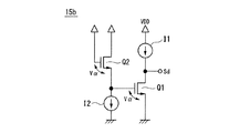
電源電圧監視回路50における信号出力回路1は、一定電流を供給する電流源回路2と、該電流源回路2からの電流を入力とするインピーダンス回路3とが直列に接続されて構成される。また、電流源回路2とインピーダンス回路3の回路接続点から信号電圧Vsigが出力される。
The
このインピーダンス回路3は、例えば、順方向にバイアスされ温度センサとして使用されるダイオード等で構成される。そして、電源の投入時において電源電圧VDDが所定の電圧に遷移するまでの間、すなわち電源電圧が低くインピーダンス回路3に供給される電流が少ない場合は、インピーダンス回路3は高インピーダンス状態を示し、信号電圧Vsigの電圧は電源電圧VDDになる。すなわち、電源電圧VDDが低い状態では、インピーダンス回路3から出力される信号電圧Vsigは、電源電圧VDDの増加と共に直線的に増加する(図4の信号電圧Vsigと電源電圧VDDを参照)。
The
そして、電源電圧VDDが増加し所定の電圧を超えた場合は、電流源回路2を通してインピーダンス回路3に流れる電流が増大するが、インピーダンス回路3に一定値以上の電流が流れると、インピーダンス回路3の両端の電圧は飽和特性を示し、一定の電圧(閾値電圧)となる。さらに、電源電圧が増加し、インピーダンス回路3に供給される電流が増加すると、インピーダンス回路3の両端の電圧は、前述の一定値から飽和特性を持って緩やかに単調増加する電圧となる。なお、インピーダンス回路3が温度センサ用のダイオード等で構成される場合には、前述の一定の電圧(閾値電圧)は温度依存性を示す電圧となる。このインピーダンス回路の詳細については、後述する。
When the power supply voltage VDD increases and exceeds a predetermined voltage, the current flowing through the
上述のインピーダンス回路3から出力される信号電圧Vsigは、信号電圧監視回路4において電源電圧VDDと比較される際の基準電圧となる信号であり、前述のように、インピーダンス回路3が温度センサ用のダイオード等で構成される場合には、温度依存性を示す信号となる。
The signal voltage Vsig output from the
電源電圧監視回路50における信号電圧監視回路4は、2つの入力端子(Tip、Tin)と出力端子Toを有する。信号電圧監視回路4は、入力される2つの信号の電位を比較し、その電位差が所定の値以上であるか否かを検出し、検出結果をローレベルまたはハイレベルの2値化された論理信号によって出力する。
The signal voltage monitoring circuit 4 in the power supply
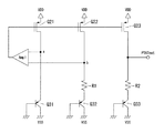
信号電圧監視回路4の一形態としてオフセットコンパレータ5を示す。オフセットコンパレータ5は、バイアス電圧源5a及びコンパレータ5bを備える。バイアス電圧源5aは、所定のバイアス電位Vbを発生させて、入力端子Tipの入力信号に対して電圧オフセットを設定する。コンパレータ5bは、入力される2つの信号の電位差を検出する。
An offset
オフセットコンパレータ5では、入力端子Tinがバイアス電圧源5aを介してコンパレータ5bの反転入力端に接続され、入力端子Tipがコンパレータ5bの非反転入力端に接続され、コンパレータ5bの出力端が出力端子Toに接続される。
In the offset
入力端子Tinに入力される信号は、バイアス電圧源5aによりバイアス電位Vb分だけ高い電位に変換され、コンパレータ5bに入力される。このような構成をとることにより、オフセットコンパレータ5は、入力端子Tipに入力された信号が、入力端子Tinに入力された信号の電圧より、所定の電圧(バイアス電位Vb)分だけ高くなった閾値電圧により比較される。
The signal input to the input terminal Tin is converted to a potential higher by the bias potential Vb by the
入力端子Tipに入力される信号VDDの電位が、入力端子Tinに入力される信号Vsigの電位にバイアス電位Vbを加算した電圧より低い状態から高い状態に遷移すると出力信号Voutが反転する。その出力信号Voutは、入力端子Tipに入力される信号VDDの電位が、入力端子Tinに入力される信号Vsigの電位にバイアス電位Vbを加算した電圧より低い状態では、ロ−レベルを示す。また、出力信号Voutは、入力端子Tipに入力される信号VDDの電位が、入力端子Tinに入力される信号Vsigの電位にバイアス電位Vbを加算した電圧より高い状態では、ハイレベルを示す。 When the potential of the signal VDD input to the input terminal Tip transitions from a state lower than a voltage obtained by adding the bias potential Vb to the potential of the signal Vsig input to the input terminal Tin, the output signal Vout is inverted. The output signal Vout is low when the potential of the signal VDD input to the input terminal Tip is lower than the voltage obtained by adding the bias potential Vb to the potential of the signal Vsig input to the input terminal Tin. The output signal Vout is at a high level when the potential of the signal VDD input to the input terminal Tip is higher than the voltage obtained by adding the bias potential Vb to the potential of the signal Vsig input to the input terminal Tin.
信号電圧監視回路4の出力電圧Voutは、後続するアプリケーション回路6に向けて出力される。アプリケーション回路6では、信号電圧監視回路4の出力電圧Voutを入力し、該出力電圧Voutがハイレベルに遷移したことを検出し、電源電圧が最低動作電源電圧を超えたことを検知する。また、信号出力回路1の信号出力Vsigも、例えば、温度センサの信号としてアプリケーション回路6に出力され、アプリケーション回路6において利用されることがある。
The output voltage Vout of the signal voltage monitoring circuit 4 is output toward the
また、図2は、信号出力回路の構成例を示す図である。図2(A)に示す例は、電流源回路2aを、参照電流Irを生成するデプレッション型のPMOSトランジスタQ13と、カレントミラー回路を構成するPMOSトランジスタQ11,Q12とで構成している。また、インピーダンス回路3aを、ゲートとドレインとを基準電位VSSに共通接続したNMOSトランジスタQ14で構成し、NMOSトランジスタQ14をダイオード(温度検出用センサ)として用いる例を示している。
FIG. 2 is a diagram illustrating a configuration example of the signal output circuit. In the example shown in FIG. 2A, the
また、図2(B)は、バックバイアスをかけたデプレッション型のPMOSランジスタQ15により電流源回路2bを構成し、インピーダンス回路3aを図2(A)と同様に、ゲートとドレインとを基準電位VSSに共通接続したNMOSトランジスタQ14で構成した例を示している。
In FIG. 2B, a depletion type PMOS transistor Q15 to which a back bias is applied constitutes a
なお、インピーダンス回路12aは、図2(A),(B)に示すNMOSトランジスタQ14に限定されず、電流源回路からの電流を入力とし、検出された物理量に応じた電圧信号を出力するセンサであればよい。例えば、図2(C)に示す温度検出用のダイオードDをインピーダンス回路として使用することができる。また、図2(D)に示すMR素子(磁気抵抗素子)をインピーダンス回路として使用することができる。さらに、図2(E)に示す、コレクタとベースを共通接地したバーポラトランジスタ素子Q15を温度センサとして使用することができる。
The
また、図3に示すような、バンドギャップレファレンス回路であってもよい。図3に示すバンドギャップレファレンス回路では、ゲートが共通接続される3つのPMOSトランジスタQ21,Q22,Q23を有している。
また、PMOSトランジスタQ21のドレインにエミッタが接続されると共に、コレクタとベースが基準電位VSSに共通接続されるバイポーラ型のPNPトランジスタQ31と、PMOSトランジスタQ22のドレインに抵抗R1を介してエミッタが接続されると共に、コレクタとベースが基準電位VSSに共通接続されるバイポーラトランジスタQ32を有している。
Further, a band gap reference circuit as shown in FIG. 3 may be used. The band gap reference circuit shown in FIG. 3 has three PMOS transistors Q21, Q22, and Q23 whose gates are commonly connected.
An emitter is connected to the drain of the PMOS transistor Q21, a bipolar PNP transistor Q31 whose collector and base are commonly connected to the reference potential VSS, and an emitter connected to the drain of the PMOS transistor Q22 via the resistor R1. And a bipolar transistor Q32 whose collector and base are commonly connected to the reference potential VSS.
さらに、PMOSトランジスタQ23のドレインに抵抗R2を介してエミッタが接続されると共に、コレクタとベースが基準電位VSSに共通接続されるバイポーラ型のPNPトランジスタQ33を有している。ここで、トランジスタQ31,Q32はエミッタ面積が1対n(n≧1)の関係を有している。 In addition, an emitter is connected to the drain of the PMOS transistor Q23 via a resistor R2, and a bipolar PNP transistor Q33 having a collector and a base commonly connected to the reference potential VSS is provided. Here, the transistors Q31 and Q32 have an emitter area of 1 to n (n ≧ 1).
また、トランジスタQ31のエミッタ側(回路点a)と、抵抗R1の回路点bとが演算増幅器Amp1の入力端子にイマジナリーショート点として入力され、算増幅器Amp1の出力端子は、PMOSトランジスタQ21,Q22,Q23のゲートに接続されている。これにより、前述の回路点aと回路点bの電位が等しくなるようにPMOSトランジスタQ21とQ22に流れる電流が制御される。また、抵抗R1とR2は同じ温度係数を持つ抵抗が選択され、例えば、抵抗R1と抵抗R2の抵抗値が等しくなるように選定する。 The emitter side (circuit point a) of the transistor Q31 and the circuit point b of the resistor R1 are input to the input terminal of the operational amplifier Amp1 as an imaginary short point, and the output terminals of the operational amplifier Amp1 are PMOS transistors Q21 and Q22. , Q23. As a result, the currents flowing through the PMOS transistors Q21 and Q22 are controlled so that the potentials at the circuit points a and b are equal. The resistors R1 and R2 are selected to have the same temperature coefficient, and are selected so that, for example, the resistance values of the resistors R1 and R2 are equal.
この構成において、PMOSトランジスタQ23が電流源回路となり、抵抗R2とトランジスタQ33がインピーダンス回路となるPTAT回路が構成され、出力電圧PTATout(PMOSトランジスタQ23のドレインの電圧)は、 In this configuration, a PTAT circuit is configured in which the PMOS transistor Q23 is a current source circuit and the resistor R2 and the transistor Q33 are impedance circuits, and the output voltage PTATout (the drain voltage of the PMOS transistor Q23) is
「PTATout=(Vt/R1)ln(N)、」
ここで、「Vt=KT/q、K:ボルツマン定数、T:絶対温度、q:電子の電荷量」
で表され、出力電圧PTAToutは絶対温度Tに比例する電圧として出力される。
“PTATout = (Vt / R1) ln (N),”
Here, “Vt = KT / q, K: Boltzmann constant, T: absolute temperature, q: electron charge”
The output voltage PTATout is output as a voltage proportional to the absolute temperature T.
このように、図3に示すバンドギャップレファレンス回路は、電流源回路(PMOSトランジスタQ23)と、インピーダンス回路(抵抗R2とバイポーラトランジスタQ33)を有しており、図1に示す信号出力回路1とすることができる。また、例えば、先行文献(特開2001−147725)において示されるバンドギャップレファレンス回路も、同様に、図1に示す信号出力回路1として用いることができる。
As described above, the bandgap reference circuit shown in FIG. 3 includes the current source circuit (PMOS transistor Q23) and the impedance circuit (resistor R2 and bipolar transistor Q33), which is the
上述したように、信号出力回路1は電流源回路とインピーダンス回路とで構成されるが、このインピーダンス回路は、電源の投入時において電源電圧VDDが所定の電圧に遷移するまでの間は、電源電圧の増加に従い直線的に増加すると共に、電源電圧が所定の電圧範囲を超えた場合に一定値の電圧、または該一定値から緩やかに単調増加する電圧を信号電圧として出力するインピーダンス回路であればよい。すなわち、インピーダンス回路は、図2に示した、トランジスタ、ダイオード、MRセンサ等、図3に示したバンドギャップレファレンス回路に限らす、例えば、ツェナーダイオード(電源に抵抗を介して接続されるツェナーダイオード)等であってもよい。
As described above, the
図4は、第1実施形態における電源電圧監視回路の動作を示すタイミングチャートである。図4に示すタイミングチャートは、図1に示す信号電圧監視回路4のA点に入力される信号電圧Vsig、B点に入力される電源電圧VDD、およびC点から出力される出力信号Voutの遷移状態を示している。 FIG. 4 is a timing chart showing the operation of the power supply voltage monitoring circuit in the first embodiment. The timing chart shown in FIG. 4 shows the transition of the signal voltage Vsig input to the point A of the signal voltage monitoring circuit 4 shown in FIG. 1, the power supply voltage VDD input to the point B, and the output signal Vout output from the point C. Indicates the state.
図に示される初期状態では、電源は未投入の状態であり、それぞれの回路において電荷の充電などもなく、各信号とも無信号の状態を示している。
時刻t1において、信号出力回路1および信号電圧監視回路4に電源が投入される。その後、電源電圧VDDが徐々に上昇する。同じ電源から電力が供給される信号出力回路1の出力である信号電圧Vsigは、電源電圧VDDが低い状態では、電流源回路2の働きにより出力電圧は電源電圧VDDになる。すなわち、信号電圧Vsigは、電源電圧VDDの上昇に応じて同様の変化特性を示して徐々に上昇する。
In the initial state shown in the figure, the power supply is not turned on, and there is no charge charging in each circuit, and each signal shows no signal.
At time t1, the
信号電圧監視回路4では、入力される信号の判定に一方の信号にオフセット電位を印加して比較することにより、入力される信号の電位差が小さな場合でもオフセットされた電位によって比較判定された結果が出力されることから出力信号がハイレベルとローレベルを交互に出力してばたつくような不安定な状態となることはない。このため信号Voutは、ローレベルを示す。すなわち、時刻t1から時刻t2までの間は、信号電圧Vsigおよび電源電圧VDDは徐々に直線的に増加するが、信号電圧Vsigと電源電圧VDDの電位差が、オフセットコンパレータ5に付与されたオフセット電位よりも小さいため、信号Voutは、ローレベルを示す。
In the signal voltage monitoring circuit 4, when an input signal is determined by applying an offset potential to one signal and making a comparison, even if the potential difference between the input signals is small, the result of the comparison determination by the offset potential is obtained. Since the output signal is output, it does not become an unstable state where the output signal flickers alternately between the high level and the low level. Therefore, the signal Vout indicates a low level. That is, between time t1 and time t2, the signal voltage Vsig and the power supply voltage VDD gradually increase linearly, but the potential difference between the signal voltage Vsig and the power supply voltage VDD is greater than the offset potential applied to the offset
電源投入後の最低動作電源電圧が供給されるまでの過渡状態においては、信号電圧監視回路4から出力される信号Voutがローレベルに維持されるため、アプリケーション回路6では、例えば、信号Voutがローレベルの場合に、例えば、自身を非活性状態に置き、不要な信号を出力しないようにできる。
In a transient state after the power is turned on until the minimum operating power supply voltage is supplied, the signal Vout output from the signal voltage monitoring circuit 4 is maintained at a low level. Therefore, in the
時刻t2では、電源電圧VDDが上昇し、それぞれの回路が動作可能な状態に遷移する。信号電圧監視回路4では、入力される信号電圧VSigと電源電圧VDDの電位差が小さな状態にあるが、一方の入力信号にはオフセット電位が印加されていることにより、信号Voutは、ローレベルに確定している。アプリケーション回路6では、信号Voutがローレベルに確定していることにより、例えば、自身を非活性状態に置き、不要な信号を出力しないようにできる。
At time t2, the power supply voltage VDD rises and transitions to a state in which each circuit can operate. In the signal voltage monitoring circuit 4, the potential difference between the input signal voltage VSig and the power supply voltage VDD is in a small state, but the offset potential is applied to one of the input signals, so that the signal Vout is fixed at a low level. is doing. In the
時刻t3では、信号V(A)によって示される信号出力回路1から出力される信号電圧Vsigが所定の電圧に到達すると、インピーダンス回路3の飽和電圧特性により、一定の電圧が出力されるようになる。電源が出力する電源電圧VDDの電位は、継続的に上昇する。また、信号電圧Vsigと電源電圧VDDの電位差は、オフセットコンパレータ5に付与されたオフセット電位よりも小さいため信号Voutは、ローレベルに維持されている。
At time t3, when the signal voltage Vsig output from the
時刻t4では、信号出力回路1から出力される信号電圧Vsigと電源電圧VDDとに、所定の電位差、すなわち信号電圧監視回路4におけるオフセット電位の電圧以上の電位差が生じたことが、信号電圧監視回路4によって検出される。その検出によって、例えば、電源によって印加される電源電圧VDDが信号出力回路1およびアプリケーション回路6に動作可能な電源電圧が供給される状態に遷移したことが示される。
At time t4, the signal voltage monitoring circuit indicates that the signal voltage Vsig output from the
これにより、信号電圧監視回路4は、信号Voutに出力していた出力信号のローレベル状態を解除し、ハイレベルに遷移させる。このハイレベルの電位は、電源電圧VDDの電位上昇にともなって上昇する。 As a result, the signal voltage monitoring circuit 4 cancels the low level state of the output signal output to the signal Vout and makes a transition to the high level. This high level potential rises as the potential of the power supply voltage VDD rises.
時刻t5では、電源電圧VDDが所定の動作可能電源電圧に達して上昇が止まり、電源電圧VDDが一定値を示すようになる。また、信号Voutの上昇も止まり一定値を示す状態に遷移する。 At time t5, the power supply voltage VDD reaches a predetermined operable power supply voltage and stops rising, and the power supply voltage VDD shows a constant value. Further, the rise of the signal Vout stops and the state changes to a state showing a constant value.
以上に示したように電源が投入されたことにより各信号の状態が遷移する。電源が出力する電源電圧VDDが所定の動作可能電源電圧に達するまで、信号Voutに不要な検出信号が出力されることなく、ローレベルを確保できる。 As described above, the state of each signal transitions when the power is turned on. Until the power supply voltage VDD output from the power supply reaches a predetermined operable power supply voltage, a low level can be secured without outputting an unnecessary detection signal as the signal Vout.
また、図5は、図1に示すアプリケーション回路の第1の例を示す図であり、後段に接続されるアプリケーション回路の例として、ボルテージフォロワ回路6aを例に挙げたものである。
FIG. 5 is a diagram showing a first example of the application circuit shown in FIG. 1, and shows an example of the
図5に示す例は、信号出力回路1内のインピーダンス回路を、NMOSトランジスタをダイオードとして使用し、温度センサとしてインピーダンス回路3bを構成した例である。また、ボルテージフォロワ回路6aにおいて、信号出力回路1から出力される信号電圧Vsigと、信号電圧監視回路4からの出力信号Voutの両方を利用する例である。
The example shown in FIG. 5 is an example in which the impedance circuit in the
このボルテージフォロワ回路6aは、カレントミラー負荷型作動入力段と、電流負荷型のソース接地利得段とで構成されるボルテージフォロワ回路であり、NMOSトランジスタQ44のゲートに入力される入力信号V/F・REFの電圧が、出力信号V/F・Outの電圧として出力される。
The
このボルテージフォロワ回路6aにおいて、カレントミラー負荷型作動入力段は、PMOSトランジスタQ41,Q42で構成されるカレントミラー回路と、作動信号がゲートに入力されるNMOSトランジスタQ43,Q44と、バイアス電流源となるNMOSトランジスタQ46,Q47とで構成されている。また、NMOSトランジスタQ43のゲートは、PMOSトランジスタQ45のドレインに接続され、ボルテージフォロワ回路が構成されている。ソース接地利得段は、PMOSトランジスタQ45とNMOSトランジスタQ47とで構成されている。
In this
上記構成において、NMOSトランジスタQ46,Q47のゲートには、信号出力回路1から出力される信号電圧Vsigが入力される。すなわち、ボルテージフォロワ回路6aにおけるバイアス電流は、信号電圧Vsigをゲートに受けるNMOSトランジスタQ46,Q47により、生成されるものとしている。
In the above configuration, the signal voltage Vsig output from the
この構成により、電源電圧VDDが上昇し、信号出力回路1からの出力信号Vsigの電圧レベルが、NMOSトランジスタQ46,Q47のゲート・ソース間の閾値を越えると、ボルテージフォロワ回路6a内のNMOSトランジスタQ46,Q47によりバイアス電流が生成され、ボルテージフォロワ回路6aとしての動作を開始することができる。このように、信号出力回路1からの信号Vsigにより、ボルテージフォロワ回路6aを直接に活性化させることができ、ボルテージフォロワ回路6aにおける最低動作電源電圧の低電圧化を図ることができる。
With this configuration, when the power supply voltage VDD rises and the voltage level of the output signal Vsig from the
また、この図5に示すボルテージフォロワ回路6aにおいては、電源VDDが低下すると、信号電圧Vsigも低下するので、バイアス電流が低下することになり、ボルテージフォロワ回路6aの動作ポイントが大きく想定から外れてしまうことが考えられる。このような場合、信号VoutによってSW1,SW2をON/OFF制御することにより、電流源Is1,Is2によりバイアス電流の低下を補うようなことが可能となる。なお、信号Voutは、信号電圧監視回路4内のオフセットコンパレータ5の出力信号である。
Further, in the
また、図6は、図1に示すアプリケーション回路の第2の例を示す図であり、後段に接続されるアプリケーション回路の例として、コンパレータ回路6bを例に挙げたものである。
FIG. 6 is a diagram illustrating a second example of the application circuit illustrated in FIG. 1, and illustrates a
図6に示す例は、信号出力回路1内のインピーダンス回路を、NMOSトランジスタをダイオードとして使用し、温度センサとしてインピーダンス回路3bを構成した例である。また、コンパレータ回路6bにおいて、信号出力回路1から出力される信号電圧Vsigと、信号電圧監視回路4からの出力信号Voutの両方を利用する例である。
The example shown in FIG. 6 is an example in which the impedance circuit in the
このコンパレータ回路6bは、図5に示すボルテージフォロワ回路6aと同様な回路構成のものであり、同一の構成部分には同一の符号を付し、重複する説明は省略する。このコンパレータ回路6bでは、NMOSトランジスタQ43,Q44のそれぞれのゲートに入力される信号Vin(1)の電圧と、Vin(2)と電圧とが比較され、比較結果が出力信号Comp・Outとして出力される。
The
この構成により、電源電圧VDDが上昇し、信号出力回路1から出力される信号電圧Vsigの電圧レベルが、NMOSトランジスタQ46,Q47のゲート・ソース間の閾値を越えると、コンパレータ回路6b内のNMOSトランジスタQ46,Q47によりバイアス電流が生成され、コンパレータ回路6bとしての動作を開始することができる。このように、信号出力回路1から出力される信号電圧Vsigにより、コンパレータ回路6bを直接に活性化させることができ、コンパレータ回路6bにおける最低動作電源電圧の低電圧化を図ることができる。
With this configuration, when the power supply voltage VDD rises and the voltage level of the signal voltage Vsig output from the
また、この図6に示すコンパレータ回路6bにおいては、電源電圧VDDが低下すると、信号電圧Vsigも低下するので、バイアス電流が低下することになり、コンパレータ回路6bの動作ポイントが大きく想定から外れてしまうことが考えられる。このような場合、VoutによってSW1,SW2をON/OFF制御することにより、電流源Is1,Is2によりバイアス電流の低下を補うようなことが可能となる。なお、信号Voutは、信号電圧監視回路4内のオフセットコンパレータ5の出力信号である。
In the
以上、本発明の第1実施形態について説明したが、図1に示す電源電圧監視回路50において、前述の信号出力回路は信号出力回路1が相当し、前述の信号電圧監視回路は信号電圧監視回路4が相当する。また、前述のオフセット機能付の比較回路はオフセットコンパレータ5が相当し、前述の電流源回路は電流源回路2が相当し、インピーダンス回路はインピーダンス回路3が相当する。
The first embodiment of the present invention has been described above. In the power supply
そして、図1に示す電源電圧監視回路50においては、温度センサ等の印加される電圧に対して飽和特性を示す信号電圧Vsigを出力する信号出力回路1と、電源電圧VDDと信号電圧Vsigとを比較し、電源電圧VDDと信号電圧Vsigとの間に所定の電圧差が発生した場合に、信号電圧Vsigが正常であることを示す信号Voutを出力する信号電圧監視回路4と、を有して構成される。
これにより、電子回路における最低動作電源電圧の低電圧化を図り、電源電圧を効率的に利用することができる。また、電源電圧VDDが所定の電圧になることを持つことなく、例え、定格動作電圧よりもかなり低い電圧であっても、この電源電圧において回路動作を許可することが可能になる。
In the power supply
As a result, the lowest operating power supply voltage in the electronic circuit can be reduced, and the power supply voltage can be used efficiently. In addition, the power supply voltage VDD does not become a predetermined voltage, and even if the voltage is considerably lower than the rated operation voltage, circuit operation can be permitted at this power supply voltage.
また、本発明の電源電圧監視回路50においては、電源から電流源回路2を通して電流の供給を受けるインピーダンス回路3を有し、このインピーダンス回路3により、信号電圧Vsigを生成して出力する信号出力回路1と、信号出力回路1から出力される信号電圧Vsigと電源電圧VDDとを比較し、電源電圧VDDと信号電圧Vsigとの間に所定の電圧差が発生した場合に、電源電圧VDDが電子回路の最低動作電源電圧以上になったことを示す信号Voutを出力する信号電圧監視回路4と、有して構成される。
これにより、電子回路における最低動作電源電圧の低電圧化を図り、電源電圧を効率的に利用することができるようになる。
Further, the power supply
As a result, the lowest operating power supply voltage in the electronic circuit can be reduced and the power supply voltage can be used efficiently.
また、本発明の電源電圧監視回路50においては、インピーダンス回路3により、電源電圧VDDと比較される基準電圧として、さらには温度依存性を示す電圧として信号電圧Vsigを生成して出力する。
これにより、例えば、温度検出用のダイオード等の温度センサの検出信号を信号電圧Vsigとし、この信号電圧Vsigを電源電圧VDDと比較して、信号電圧Vsigが正常であること示す信号Voutを出力することができる。
In the power supply
Accordingly, for example, a detection signal of a temperature sensor such as a temperature detection diode is set as the signal voltage Vsig, and the signal voltage Vsig is compared with the power supply voltage VDD, and a signal Vout indicating that the signal voltage Vsig is normal is output. be able to.
また、本発明の電源電圧監視回路50においては、信号出力回路1は、電源の投入時に電源電圧VDDが所定の電圧になるまでは、電源電圧VDDの増加に従い増加する電圧を信号電圧Vsigとして出力すると共に、電源電圧VDDが所定の電圧を超えて増加する場合に、飽和特性を持って単調増加する電圧を信号電圧Vsigとして出力する。信号電圧監視回路4は、信号出力回路1から出力される信号電圧Vsigと電源電圧VDDとを比較し、電源電圧VDDと信号電圧Vsigとの間に所定の電圧差が発生した場合に、電源電圧VDDが電子回路における最低動作電源電圧以上になったことを示す信号Voutを出力する。
これにより、電子化路における最低動作電源電圧の低電圧化を図り、電源電圧を効率的に利用することができるようになる。
Further, in the power supply
As a result, the lowest operating power supply voltage in the electronic path can be reduced, and the power supply voltage can be used efficiently.
また、本発明の電源電圧監視回路においては、信号電圧監視回路4は、オフセット電位が一方の入力に設定される比較器(オフセットコンパレータ5)を有し、この比較器(オフセットコンパレータ5)により信号出力回路1から出力される信号電圧Vsigと電源電圧VDDとを比較し、信号出力回路1から出力される信号電圧Vsigと電源電圧VDDの電位差がオフセット電位を満たす場合に電源電圧VDDが最低動作電源電圧を超えたことを示す信号Voutを出力する。
これにより、信号出力回路からの信号とオフセット電位とを基に、電子回路における最低動作電源電圧を容易に検出することができる。
In the power supply voltage monitoring circuit of the present invention, the signal voltage monitoring circuit 4 has a comparator (offset comparator 5) in which the offset potential is set to one input, and the comparator (offset comparator 5) outputs a signal. The signal voltage Vsig output from the
Thereby, the minimum operating power supply voltage in the electronic circuit can be easily detected based on the signal from the signal output circuit and the offset potential.
また、本発明の電源電圧監視回路50においては、信号出力回路1は、電流源回路2とインピーダンス回路3とが直列に接続されて構成され、電流源回路2とインピーダンス回路3との回路接続点から信号電圧が出力される。
これにより、例えば、インピーダンス回路として順方向にバイアスされたダイード等を使用して信号出力回路1を容易に構成することができる。また、インピーダンス回路を温度センサ等で構成することができる。
In the power supply
Thus, for example, the
また、本発明の電源電圧監視回路50においては、インピーダンス回路3は、電流源回路2から出力される電流を入力とし、検出された物理量に応じた電圧信号を出力するセンサである。
これにより、センサからの出力信号を検出対象として、センサが安定して動作できる電源電圧のレベルを検出することができる。このため、センサが安定して動作できる電圧を電子回路の最低動作電源電圧とすることができ、電子回路における最低動作電源電圧の低電圧化を図り、電源電圧を効率的に利用することができるようになる。
In the power supply
Thereby, the level of the power supply voltage at which the sensor can operate stably can be detected using the output signal from the sensor as a detection target. For this reason, the voltage at which the sensor can operate stably can be set as the minimum operating power supply voltage of the electronic circuit, the minimum operating power supply voltage in the electronic circuit can be reduced, and the power supply voltage can be used efficiently. It becomes like this.
また、本発明の電源電圧監視回路50においては、インピーダンス回路3は、電流源回路2から出力される電流を入力とし、検出された温度に応じた電圧信号を出力する温度センサである。
これにより、温度センサからの出力信号を検出対象として、この温度センサが安定して動作できる電源電圧のレベルを検出することができる。このため、温度センサが安定して動作できる電圧を電子回路の最低動作電源電圧とすることができ、電子回路における最低動作電源電圧の低電圧化を図り、電源電圧を効率的に利用することができるようになる。
In the power supply
As a result, the level of the power supply voltage at which the temperature sensor can operate stably can be detected using the output signal from the temperature sensor as a detection target. For this reason, the voltage at which the temperature sensor can operate stably can be set as the minimum operating power supply voltage of the electronic circuit, the minimum operating power supply voltage in the electronic circuit can be reduced, and the power supply voltage can be used efficiently. become able to.
また、本発明の電子回路は、本発明の電源電圧監視回路を備えるので、これにより、電子回路における最低動作電源電圧の低電圧化を図り、電源電圧を効率的に利用することができるようになる。 In addition, since the electronic circuit of the present invention includes the power supply voltage monitoring circuit of the present invention, it is possible to reduce the minimum operating power supply voltage in the electronic circuit and to efficiently use the power supply voltage. Become.
(第2実施形態)
図7は、第2実施形態による検出回路を示す概略構成図である。この第2の実施の形態では、図1に示す第1の実施の形態の電源電圧監視回路の応用例であり、温度センサ等の信号を検出する検出回路の例を示したものである。
(Second Embodiment)
FIG. 7 is a schematic configuration diagram illustrating a detection circuit according to the second embodiment. The second embodiment is an application example of the power supply voltage monitoring circuit of the first embodiment shown in FIG. 1, and shows an example of a detection circuit that detects a signal from a temperature sensor or the like.
この図7に示す第2の実施の形態では、図1に示す信号出力回路1中のインピーダンス回路を、例えば、図2に示すようにダイオード等の温度センサとして構成し、この温度センサから信号される信号をVtempとしたものである。すなわち、図1に示す信号出力回路1から出力される信号電圧Vsigを、温度センサの出力信号Vtempとしたものである。また、図1に示す信号電圧監視回路4を、図7に示す割込条件生成回路10aとして使用した例を示したものである。
In the second embodiment shown in FIG. 7, the impedance circuit in the
なお、後述する第3実施形態から第8実施の形態において説明される検出回路、および第9実施形態のセンサ装置も、図1に示す本発明の電源電圧監視回路の応用例として示されるものである。また、図1の信号電圧監視回路4を構成するオフセットコンパレータ5が、第4実施形態から第7の実施形態における割込条件生成回路中のオフセットコンパレータ11に相当するものである。
Note that the detection circuits described in the third to eighth embodiments, which will be described later, and the sensor device of the ninth embodiment are also shown as application examples of the power supply voltage monitoring circuit of the present invention shown in FIG. is there. Further, the offset
図7に示す検出回路100は、割込条件生成回路10a、割込条件受付回路20a及びコンパレータ30を備える。
検出回路100における割込条件生成回路10aは、2つの入力端子(Tip、Tin)と出力端子Toを有する。割込条件生成回路10aは、入力される2つの信号の電位を比較し、その電位差が所定の値以上であるか否かを検出し、検出結果を2値化された論理信号によって出力する。
The
The interrupt
割込条件生成回路10aの一形態としてオフセットコンパレータ11を示す。オフセットコンパレータ11は、バイアス電圧源11b及びコンパレータ11cを備える。バイアス電圧源11bは、所定のバイアス電位Vbを発生させて、入力される信号に発生させた電位分の電圧オフセットを設定する。コンパレータ11cは、入力される2つの信号の電位差を検出する。
オフセットコンパレータ11では、入力端子Tinがバイアス電圧源11bを介してコンパレータ11cの反転入力端に接続され、入力端子Tipがコンパレータ11cの非反転入力端に接続され、コンパレータ11cの出力端が出力端子Toに接続される。
入力端子Tinに入力される信号は、バイアス電圧源11bによりバイアス電位Vb分だけ高い電位に変換され、コンパレータ11cに入力される。
このような構成をとることにより、オフセットコンパレータ11は、入力端子Tipに入力された信号の電圧が、入力端子Tinに入力された信号の電圧より、所定の電圧(バイアス電位Vb)分だけ高くなった閾値電圧により比較される。入力端子Tipに入力される信号の電位が、入力端子Tinに入力される信号の電位にバイアス電位Vbを加算した電圧より低い状態から高い状態に遷移すると出力信号が反転する。その出力信号は、前者の状態(バイアス電位Vbを加算した電圧より低い状態)では、ローレベルを示す。
割込条件生成回路10aからは、オフセットコンパレータ11の出力と同じ信号が出力される。
An offset
In the offset
The signal input to the input terminal Tin is converted to a potential higher by the bias potential Vb by the
By adopting such a configuration, the offset
The same signal as the output of the offset
割込条件受付回路20aは、信号入力端子Inと制御入力端子Contと出力端子Outを有する。
割込条件受付回路20aの一形態として出力設定回路21を示す。出力設定回路21は、インバータ(反転回路)21a及びNAND(反転論理積)ゲート21bを備える。出力設定回路21では、信号入力端子InがNANDゲート21bの一方の入力端に接続され、制御入力端子ContがNANDゲート21bの他方の入力端に接続され、NANDゲート21bの出力端がインバータ21aを介して出力端子Outに接続される。このような構成をとることにより、制御入力端子Contに入力される制御信号Scontがローレベルの場合には、出力信号Voutがローレベルに設定され、制御信号Scontがローレベルの場合には、入力される信号Sgと同じ論理を示す信号が出力信号Voutに出力される。すなわち、割込条件受付回路20aは、制御信号として入力される割込信号による割込みが解除されるまで、入力される信号Sgの出力を許可せずローレベルを示す所定の電圧を出力信号Voutとして出力する。また、割込条件受付回路20aは、割込信号による割込みが解除されると、入力される信号Sgの出力を許可して出力信号Voutとして出力する。
コンパレータ30は、入力される2つの信号の電位差を検出し、検出した電位差に基づいて判定した結果を2値化した論理信号で出力する。
The interrupt
An
The
次に、センサ回路を構成する検出回路100の接続例を示す。検出回路100には、検出回路100を作動させる電源電圧VDDと、図示されないセンサ回路からの入力信号Vtempと、図示されない基準電源RFから出力される基準電圧Vrefとが入力される。図示されないセンサ回路及び基準電源RFは、電源に接続される電源端子に定電流源が接続され、その定電流源の負荷となるインピーダンス素子を介して接地電圧VSSに接続される。それぞれの出力は、定電流源とインピーダンス素子との接続点から出力される。よって、電源電圧VDDが低い状態では、これらの出力電圧は電流源の働きにより電源電圧になる。
割込条件生成回路10aにおける入力端子Tipには、電源が接続され電源電圧VDDが入力される。また、入力端子Tinには、図示されないセンサ回路の出力端が接続される。
コンパレータ30における非反転入力端子には、基準電圧Vrefを出力する図示されない基準電源RFが接続され、反転入力端子には、図示されないセンサ回路の出力端が接続される。
割込条件受付回路20aにおける入力端子Inにはコンパレータ30の出力端が接続され、制御入力端子Contには割込条件生成回路10aの出力端子Toが接続され、出力端子Toが検出回路100の出力端子に接続される。
Next, a connection example of the
A power supply is connected to the input terminal Tip in the interrupt
A reference power supply RF (not shown) that outputs a reference voltage Vref is connected to the non-inverting input terminal of the
The output terminal of the
このような構成による検出回路100では、割込条件生成回路10aから出力される制御信号Scontは、電源電圧VDDが入力信号Vtempの電圧にバイアス電位Vb加算した電位より低い場合にはローレベルを示す。また、割込条件生成回路10aから出力される制御信号Scontは、電源電圧VDDが入力信号Vtempの電圧にバイアス電位Vb加算した電位より高い場合にはハイレベルを示す。
コンパレータ30の出力信号Sgは、入力信号Vtempの電圧が基準電圧Vrefより低い場合にはハイレベルを示す。また、入力信号Vtempの電圧が基準電圧Vrefより高い場合にはローレベルを示す。
割込条件受付回路20aの出力信号Voutには、制御信号Scontがローレベルの場合には、固定的にローレベルが出力され、制御信号Scontがハイレベルの場合には、入力信号Vtempに応じて変化するコンパレータ30からの出力信号Sgが出力される。
In the
The output signal Sg of the
When the control signal Scont is at a low level, the output signal Vout of the interrupt
図8は、第2実施形態における検出回路100の動作を示すタイミングチャートの例である。図7のブロック図に示された点A〜Hにしたがって、それらの点における各信号の遷移について説明する。
点Aの波形は、センサ回路から入力され、検出回路100が検出処理をする入力信号Vtempの電圧遷移を示す。点Bの波形は、検出回路100に供給される電源電圧VDDの電圧遷移を示す。この電源電圧VDDは、検出回路100並びに図7に図示されていない基準電源RF及びセンサ回路に供給されている電源電圧を示す。点Cの波形は、割込条件生成回路10aにおけるオフセットコンパレータ11によって判定され、割込条件生成回路10aから出力された制御信号Scontの電圧遷移を示す。この信号に基づいて、割込条件受付回路20aが制御される。点Fの波形は、基準電源RFから出力される基準電圧Vrefの電圧遷移を示す。点Gの波形は、コンパレータ30による判定結果である出力信号Sgの電圧遷移を示す。この信号は、割込条件受付回路20aへの入力信号になる。点Hの波形は、割込条件受付回路20aの出力信号Voutの電圧遷移を示す。このタイミングチャートに示される範囲では、センサ回路によって検出すべき事象は生じていない状態を示し、出力信号Voutは、常時ローレベルを示す。
FIG. 8 is an example of a timing chart showing the operation of the
The waveform at point A indicates the voltage transition of the input signal Vtemp that is input from the sensor circuit and subjected to detection processing by the
図に示される初期状態では、電源は未投入の状態であり、それぞれの回路において電荷の充電などもなく、各信号とも無信号の状態を示している。
時刻t1において、検出回路100並びに検出回路100に接続されているセンサ回路及び基準電源RFに対し、電源が投入される。
その後、電源電圧VDDが徐々に上昇する。同じ電源から電力が供給されるセンサ回路及び基準電源RFの出力である入力信号Vtemp及び基準電圧Vrefは、電源電圧VDDが低い状態では、電流源の働きによりこれらの出力電圧は電源電圧VDDになる。入力信号Vtemp及び基準電圧Vrefは、電源電圧VDDの上昇に応じて同様の変化特性を示して徐々に上昇する。
割込条件生成回路10aでは、入力される信号の判定に一方の信号にオフセット電位を印加して比較することにより、入力される信号の電位差が小さな場合でもオフセットされた電位によって比較判定された結果が出力されることから出力信号がハイレベルとローレベルを交互に出力してばたつくような不安定な状態となることはない。このため制御信号Scontは、ローレベルを示す。
In the initial state shown in the figure, the power supply is not turned on, and there is no charge charging in each circuit, and each signal shows no signal.
At time t1, power is turned on to the
Thereafter, the power supply voltage VDD gradually increases. The sensor circuit to which power is supplied from the same power source and the input signal Vtemp and the reference voltage Vref, which are the outputs of the reference power supply RF, become the power supply voltage VDD by the action of the current source when the power supply voltage VDD is low. . The input signal Vtemp and the reference voltage Vref gradually increase with the same change characteristics as the power supply voltage VDD increases.
In the interrupt
検出回路100では、電源投入後の動作可能電源電圧が供給されるまでの過度状態においては、コンパレータ30の出力信号Sgに不要な検出信号が出力されることがある。つまり、コンパレータ30が備える入力信号判定回路が正常に動作するために必要な電源電圧に到達していないために、出力信号Sgは、信号の状態を特定できない不定状態となる。
一方、割込条件受付回路20aは、電源電圧が所定の電圧に達するまで入力信号の出力を許可せず所定の電圧を出力信号Voutとして出力する。出力信号Voutとして出力される所定の電圧は、センサ回路において非検出状態(解除状態)を示す電圧が設定され、制御信号Scontに応じて制御される。制御信号Scontには、ローレベルが出力されていることにより、出力信号Voutがローレベルに確保され、不要な検出状態を示す信号が出力されることはない。
In the
On the other hand, the interrupt
時刻t2では、電源電圧VDDが上昇し、それぞれの回路が動作可能な状態に遷移する。
割込条件生成回路10aでは、入力信号Vtempは電源電圧VDDの上昇にしたがって上昇するため、その電位差が小さな状態にある。一方の信号にはオフセット電位が印加されていることにより、出力される制御信号Scontは、ローレベルに確定している。センサ回路及び基準電源RFの出力である入力信号Vtemp及び基準電圧Vrefも電源電圧VDDの上昇にしたがって徐々に上昇するため、その電位差が小さな状態にある。電位差が小さい2つの信号を比較して得られる出力信号Sgは、信号の状態を特定できない不定状態が継続する。割込条件受付回路20aでは、制御信号Scontがローレベルに確定していることにより、出力信号Voutがローレベルに確保され、不要な検出状態を示す信号が出力されることはない。
At time t2, the power supply voltage VDD rises and transitions to a state in which each circuit can operate.
In the interrupt
時刻t3では、基準電源RFから入力される基準電圧Vrefが所定の電圧に到達すると定電圧制御され、一定の電圧が入力されるようになる。電源電圧VDD及びセンサ回路からの入力信号Vtempの電位は、継続的に上昇する。
基準電圧Vrefが所定の電圧を示すようになり、基準電圧Vrefは入力信号Vtempより低い電位を示すことから、出力信号Sgは、状態が定まらない不定状態から正しい判定結果が出力される状態に遷移する。また、制御信号Scontによる制御が継続されることにより、出力信号Voutはローレベルに確保され、不要な検出状態を示す信号が出力されることはない。
At time t3, when the reference voltage Vref input from the reference power supply RF reaches a predetermined voltage, constant voltage control is performed, and a constant voltage is input. The power supply voltage VDD and the potential of the input signal Vtemp from the sensor circuit continuously rise.
Since the reference voltage Vref indicates a predetermined voltage and the reference voltage Vref indicates a potential lower than the input signal Vtemp, the output signal Sg changes from an indefinite state where the state is not determined to a state where a correct determination result is output. To do. Further, by continuing the control by the control signal Scont, the output signal Vout is secured at a low level, and a signal indicating an unnecessary detection state is not output.
時刻t4では、センサ回路からの入力信号Vtempは、所定の検出状態を示す定常動作状態に遷移する。これにより、センサ回路が検出する状態によって入力信号Vtempは変化することになり、これまで継続していた電源電圧VDDの上昇にともなう上昇は停止する。そして、センサ回路が備える定電流回路が供給する電流とセンサ回路のインピーダンスによって定まる入力信号Vtempの電圧値より、電源電圧VDDの方が高くなったことにより、センサ回路からの入力信号Vtempによる変化が検出できるようになる。
時刻t5では、センサ回路からの入力信号Vtempと電源電圧VDDとに、所定の電位差、すなわち割込条件生成回路10aにおけるオフセット電位の電圧以上の電位差が生じることを、割込条件生成回路10aによって検出される。その検出によって、電源電圧VDDがセンサ回路に動作可能な電源電圧が供給される状態に遷移したことが示される。割込条件生成回路10aでは、制御信号Scontの割込み状態(ローレベル)を解除することにより、制御信号Scontの電圧が電源電圧VDDの電位上昇にともなって上昇する。
時刻t6では、電源電圧VDDが所定の動作可能電源電圧に達して上昇が止まり、電源電圧VDDが一定値を示すようになる。また、制御信号Scontの電圧上昇も止まり一定値を示す状態に遷移する。
以上に示したように電源が投入されたことにより各信号の状態が遷移する。電源電圧VDDが所定の動作可能電源電圧に達するまで、出力信号Voutはローレベルに確保され、不要な検出状態を示す信号が出力されることはない。
At time t4, the input signal Vtemp from the sensor circuit transits to a steady operation state indicating a predetermined detection state. As a result, the input signal Vtemp changes depending on the state detected by the sensor circuit, and the rise accompanying the rise of the power supply voltage VDD that has been continued is stopped. Since the power supply voltage VDD is higher than the voltage value of the input signal Vtemp determined by the current supplied by the constant current circuit included in the sensor circuit and the impedance of the sensor circuit, the change due to the input signal Vtemp from the sensor circuit is changed. Can be detected.
At time t5, the interrupt
At time t6, the power supply voltage VDD reaches a predetermined operable power supply voltage and stops rising, and the power supply voltage VDD shows a constant value. In addition, the voltage rise of the control signal Scont stops and the state changes to a state showing a constant value.
As described above, the state of each signal transitions when the power is turned on. Until the power supply voltage VDD reaches a predetermined operable power supply voltage, the output signal Vout is secured at a low level, and a signal indicating an unnecessary detection state is not output.
(第3実施形態)
図を参照し、形態の異なる検出回路の実施形態について示す。
図9は、第3実施形態による検出回路を示す概略構成図である。図9に示す例では、図7に示す第2の実施の形態における割込条件生成回路10a(図1に示す信号電圧監視回路4と同じ構成の回路)に代えて、POC(Power On Clear)回路12を使用する例を示したものである。これは、後述する実施の形態の説明において、図9に示すPOC回路12と、図7に示す割込条件生成回路10aとを併用して使用する場合があるため、ここでPOC回路12を使用する検出回路の例について説明しておくものである。
(Third embodiment)
With reference to the drawings, embodiments of detection circuits having different forms will be described.
FIG. 9 is a schematic configuration diagram illustrating a detection circuit according to the third embodiment. In the example shown in FIG. 9, POC (Power On Clear) is used instead of the interrupt
図9に示す検出回路200は、割込条件生成回路10b、割込条件受付回路20a及びコンパレータ30を備える。図7と同じ構成には同じ符号を付し、異なる構成について説明する。
検出回路200における割込条件生成回路10bは、電源投入時に所定時間の間、初期状態を保持する信号を出力する。割込条件生成回路10bは、POC(Power On Clear)回路12からなる。POC回路12は、いわゆる電源投入初期化回路である。
POC回路12は、直列に接続されたコンデンサ12Cと抵抗12Rは、電源(電源電圧VDD)にコンデンサ12Cの一端が接続され、基準となる電源(接地電圧VSS)に抵抗12Rの一端が接続される。コンデンサ12Cと抵抗12Rの接続点は、インバータ(NOT回路)12aの入力端に接続され、インバータ12aが割込条件生成回路10bの制御信号Scontを出力する。
この割込条件生成回路10bの出力は、割込条件受付回路20aの制御入力端子Contに接続される。
The
The interrupt
In the
The output of the interrupt
このような構成による検出回路200では、割込条件生成回路10bから出力される制御信号Scontは、電源の投入後、所定の時間経過するまでローレベルを示し、所定の時間経過するとハイレベルを示す。
コンパレータ30の出力信号Sgは、入力信号Vtempの電圧が基準電圧Vrefより低い場合にはハイレベルを示す。また、コンパレータ30の出力信号Sgは、入力信号Vtempの電圧が基準電圧Vrefより高い場合にはローレベルを示す。
割込条件受付回路20aの出力信号Voutは、制御信号Scontがローレベルの場合には固定的にローレベルが出力され、制御信号Scontがハイレベルの場合には入力信号Vtempに応じて変化するコンパレータ30の出力信号Sgが出力される。
In the
The output signal Sg of the
The output signal Vout of the interrupt
図10は、第3実施形態における検出回路の動作を示すタイミングチャートである。
図9のブロック図に示された点A〜H、点P及び点Vdにしたがって、それらの点における各信号の遷移について説明する。図8と同じ信号、時刻には同じ符号を付し、異なる信号、時刻を中心に説明する。図8に示した検出回路100は、検出回路200と読み替える。
点の波形VDDは、POC回路12の電源電圧VDDの電圧遷移を示す。点Vdの波形は、POC回路12におけるCR回路の接合点Vdの電圧遷移を示す。点Pの波形は、割込条件生成回路10bにおけるPOC回路12よって判定され、出力された制御信号Scontの電圧遷移を示す。この信号に基づいて、割込条件受付回路20aが制御される。
FIG. 10 is a timing chart showing the operation of the detection circuit in the third embodiment.
The transition of each signal at these points will be described according to points A to H, point P, and point Vd shown in the block diagram of FIG. The same signals and times as those in FIG. 8 are denoted by the same reference numerals, and different signals and times will be mainly described. The
A point waveform VDD indicates a voltage transition of the power supply voltage VDD of the
図に示される初期状態では、電源は未投入の状態であり、それぞれの回路において電荷の充電などもなく、各信号とも無信号の状態を示している。
時刻t1において、検出回路200並びに検出回路200に接続されているセンサ回路及び基準電源RFに対し、電源が投入される。その後、電源電圧VDDが徐々に上昇する。センサ回路及び基準電源RFの出力である入力信号Vtemp及び基準電圧Vrefは、電源電圧VDDが低い状態では、電流源の働きによりこれらの出力電圧は電源電圧になる。入力信号Vtemp及び基準電圧Vrefは、電源電圧VDDの上昇に応じて同様の変化特性を示して徐々に上昇する。
割込条件生成回路10bにおけるPOC回路12では、電源電圧VDDを検出する。
コンデンサ12Cと抵抗12Rからなる時定数回路により、電源電圧VDDを入力としたステップ応答として同定される一次遅れの過度特性により点Vdの電位が遷移する。電源投入に追従して点Vdの電位が上昇するが、インバータ12aがまだ活性化されないことから制御信号Scontはローレベルを示す。
In the initial state shown in the figure, the power supply is not turned on, and there is no charge charging in each circuit, and each signal shows no signal.
At time t1, power is turned on to the
The
By the time constant circuit composed of the capacitor 12C and the
検出回路200では、電源投入後の動作可能電源電圧が供給されるまでの過度状態にあり、コンパレータ30の出力信号Sgは、信号の状態を特定できない不定状態となる。
一方、割込条件受付回路20aは、電源電圧VDDが所定の電圧に達するまで入力信号の出力を許可せず所定の電圧を出力信号Voutとして出力する。出力信号Voutとして出力される所定の電圧は、センサ回路において非検出状態(解除状態)を示す電圧が設定され、制御信号Scontに応じて制御される。制御信号Scontには、ローレベルが出力されていることにより、出力信号Voutはローレベルに確保され、不要な検出状態を示す信号が出力されることはない。
The
On the other hand, the interrupt
時刻t2では、電源電圧VDDが上昇し、それぞれの回路が動作可能な状態に遷移する。
割込条件生成回路10bにおけるPOC回路12では、点Vdの電位がインバータ12aにおける閾値電位より高い状態を示す。インバータ12aの電源電圧が過度的に上昇するにつれインバータ12aの閾値電位も電源電圧の上昇に応じて上昇する。これにより、制御信号Scontは、ローレベルに確定している。センサ回路及び基準電源RFの出力である入力信号Vtemp及び基準電圧Vrefも電源電圧VDDの上昇にしたがって徐々に上昇するため、その電位差が小さな状態にある。電位差が小さい2つの信号を比較して得られる出力信号Sgは、信号の状態を特定できない不定状態が継続する。割込条件受付回路20aでは、制御信号Scontがローレベルに確定していることにより、出力信号Voutはローレベルに確保され、不要な検出状態を示す信号が出力されることはない。
At time t2, the power supply voltage VDD rises and transitions to a state in which each circuit can operate.
In the
時刻t3では、基準電源RFから入力される基準電圧Vrefが所定の電圧に到達すると定電圧制御され、一定の電圧が入力されるようになる。電源電圧VDD及びセンサ回路からの入力信号Vtempの電位は、継続的に上昇する。
基準電圧Vrefが所定の電圧を示すようになり、基準電圧Vrefは入力信号Vtempより低い電位を示すことから、出力信号Sgは、状態が定まらない不定状態から正しい判定結果が出力される状態に遷移する。また、制御信号Scontによる制御が継続されることにより、出力信号Voutはローレベルに確保され、不要な検出状態を示す信号が出力されることはない。
At time t3, when the reference voltage Vref input from the reference power supply RF reaches a predetermined voltage, constant voltage control is performed, and a constant voltage is input. The power supply voltage VDD and the potential of the input signal Vtemp from the sensor circuit continuously rise.
Since the reference voltage Vref indicates a predetermined voltage and the reference voltage Vref indicates a potential lower than the input signal Vtemp, the output signal Sg changes from an indefinite state where the state is not determined to a state where a correct determination result is output. To do. Further, by continuing the control by the control signal Scont, the output signal Vout is secured at a low level, and a signal indicating an unnecessary detection state is not output.
時刻t4では、センサ回路からの入力信号Vtempは、所定の検出状態を示す定常動作状態に遷移する。これにより、センサ回路が検出する状態によって入力信号Vtempは変化することになり、これまで継続していた電源電圧VDDの上昇にともなう上昇は停止する。そして、センサ回路が備える定電流回路が供給する電流とセンサ回路のインピーダンスとによって定まる入力信号Vtempの電圧値より、電源電圧VDDの方が高くなったことにより、センサ回路からの入力信号Vtempによる変化が検出できるようになる。
時刻t6では、電源電圧VDDが所定の動作可能電源電圧に達して上昇が止まり、電源電圧VDDが一定値を示すようになる。また、制御信号Scontの電位の上昇も止まり一定値を示す状態に遷移する。
割込条件生成回路10bにおけるPOC回路12では、電源電圧VDDが定電圧制御に遷移したことから、点Vdの電位上昇が止まり降下に転じる。
時刻t7では、割込条件生成回路10bにおけるPOC回路12では、点Vdの電位がインバータ12aの閾値電圧以下に低下したことにより制御信号Scontがハイレベルに遷移する。割込条件生成回路10bは、制御信号Scontに出力していた制御信号の割込み状態(ローレベル)を解除する。これにより、検出回路200は、検出信号の出力が行える通常状態に遷移する。
以上に示したように電源が投入されたことにより各信号の状態が遷移する。電源電圧VDDが所定の動作可能電源電圧に達するまで、出力信号Voutはローレベルに確保され、不要な検出状態を示す信号が出力されることはない。
At time t4, the input signal Vtemp from the sensor circuit transits to a steady operation state indicating a predetermined detection state. As a result, the input signal Vtemp changes depending on the state detected by the sensor circuit, and the rise accompanying the rise of the power supply voltage VDD that has been continued is stopped. Then, since the power supply voltage VDD is higher than the voltage value of the input signal Vtemp determined by the current supplied by the constant current circuit included in the sensor circuit and the impedance of the sensor circuit, the change due to the input signal Vtemp from the sensor circuit Can be detected.
At time t6, the power supply voltage VDD reaches a predetermined operable power supply voltage and stops rising, and the power supply voltage VDD shows a constant value. In addition, the rise of the potential of the control signal Scont stops and the state changes to a state showing a constant value.
In the
At time t7, in the
As described above, the state of each signal transitions when the power is turned on. Until the power supply voltage VDD reaches a predetermined operable power supply voltage, the output signal Vout is secured at a low level, and a signal indicating an unnecessary detection state is not output.
(第4実施形態)
図を参照し、形態の異なる検出回路の実施形態について示す。
図11は、第4実施形態による検出回路を示す概略構成図である。
検出回路300は、割込条件生成回路10c、割込条件受付回路20a及びコンパレータ30を備える。図7及び図9と同じ構成には同じ符号を付し、異なる構成について説明する。
検出回路300において割込条件生成回路10cは、オフセットコンパレータ11、POC回路13及びRSフリップフロップ14を備える。
POC回路13は、いわゆる電源投入初期化回路である。
POC回路13は、直列に接続されたコンデンサ13Cと抵抗13Rは、電源の正極(電源電圧VDD)にコンデンサ13Cの一端が接続され、電源の負極(接地電圧VSS)に抵抗13Rの一端が接続される。コンデンサ13Cと抵抗13Rの接続点は、バッファ13bの入力端に接続される。バッファ13bは、入力される電圧(点Vdの電圧)がバッファ13bの閾値電圧(反転電圧)以上になると、出力する信号Sp’が電源電圧VDDによって示されるハイレベルになり、閾値電圧(反転電圧)以下になると、信号Sp’が基準電圧VSSによって示されるローレベルになる。バッファ13bから出力される信号は、POC回路13の出力信号となる。Vdがバッファ13bの反転電圧以上になると、信号Sp’が電源電圧VDDになり、反転電圧以下になると、信号Sp’が基準電圧VSSになる。バッファ13bの閾値電圧は、電源電圧VDDの半分の電圧になる。
オフセットコンパレータ11は、信号Scを出力する。信号Scは、実施形態における制御信号Scontに相当する。
RSフリップフロップ14は、RS型フリップフロップを示す。
(Fourth embodiment)
With reference to the drawings, embodiments of detection circuits having different forms will be described.
FIG. 11 is a schematic configuration diagram illustrating a detection circuit according to the fourth embodiment.
The
In the
The
In the
The offset
The RS flip-
オフセットコンパレータ11の出力端がRSフリップフロップ14のセット入力端(S)に接続され、POC回路13の出力端がRSフリップフロップ14のリセット入力端(R)に接続され、RSフリップフロップ14の出力端が割込条件生成回路10cの制御信号Scontを出力する。RSフリップフロップ14は、セット入力端(S)及びリセット入力端(R)にハイレベルが入力された場合は、それぞれ出力信号をハイレベル(セット)及びローレベル(リセット)に設定し、ともにハイレベルが入力されるとリセット要求を優先させてローレベル(リセット)を設定する。
The output terminal of the offset
このような構成による検出回路300では、割込条件生成回路10cから出力される制御信号Scontは、電源電圧VDDが入力信号Vtempの電圧にバイアス電位Vb加算した電位より低い場合にはローレベルを示す。また、制御信号Scontは、電源電圧VDDが入力信号Vtempの電圧にバイアス電位Vb加算した電位より高い場合にはハイレベルを示す。
割込条件生成回路10cから出力される制御信号Scontは、電源の投入後、所定の時間経過するまでハイレベルを示し、所定の時間経過するとローレベルを示す。
In the
The control signal Scont output from the interrupt
コンパレータ30の出力信号Sgは、入力信号Vtempの電圧が基準電圧Vrefより低い場合にはハイレベルを示す。また、入力信号Vtempの電圧が基準電圧Vrefより高い場合にはローレベルを示す。
割込条件受付回路20aの出力信号Voutは、制御信号Scontがローレベルの場合には固定的にローレベルが出力され、制御信号Scontがハイレベルの場合には入力信号Vtempに応じて変化するコンパレータ30の出力信号Sgが出力される。
The output signal Sg of the
The output signal Vout of the interrupt
図12は、第4実施形態における検出回路の動作を示すタイミングチャートである。
図11のブロック図に示された点A〜H及び点P’にしたがって、それらの点における各信号の遷移について説明する。図8及び図10と同じ信号、時刻には同じ符号を付し、異なる信号、時刻を中心に説明する。図8に示した検出回路100及び図10に示した検出回路200は、検出回路300と読み替える。
点Cの波形は、割込条件生成回路10cにおけるオフセットコンパレータ11から出力される信号Scの電圧遷移を示す。点Eの波形は、割込条件生成回路10cにおけるRSフリップフロップ14から出力される制御信号Scontを示す。点P’の波形は、割込条件生成回路10cにおけるPOC回路13から出力される信号Sp’の電圧遷移を示す。
FIG. 12 is a timing chart showing the operation of the detection circuit in the fourth embodiment.
The transition of each signal at the points A to H and the point P ′ shown in the block diagram of FIG. 11 will be described. The same signals and times as those in FIGS. 8 and 10 are given the same reference numerals, and different signals and times will be mainly described. The
A waveform at the point C indicates a voltage transition of the signal Sc output from the offset
図に示される初期状態では、電源は未投入の状態であり、それぞれの回路において電荷の充電などもなく、各信号とも無信号の状態を示している。
時刻t1において、検出回路300並びに検出回路300に接続されているセンサ回路及び基準電源RFに対し、電源が投入される。その後、電源電圧VDDが徐々に上昇する。センサ回路及び基準電源RFの出力である入力信号Vtemp及び基準電圧Vrefは、電源電圧VDDが低い状態では、電流源の働きによりこれらの出力電圧は電源電圧になる。入力信号Vtemp及び基準電圧Vrefは、電源電圧VDDの上昇に応じて同様の変化特性を示して徐々に上昇する。
検出回路300では、電源投入後の動作可能電源電圧が供給されるまでの過度状態にあり、コンパレータ30の出力信号Sgは、信号の状態を特定できない不定状態となる。
In the initial state shown in the figure, the power supply is not turned on, and there is no charge charging in each circuit, and each signal shows no signal.
At time t1, power is turned on to the
The
割込条件生成回路10cにおけるオフセットコンパレータ11では、入力される信号の判定に一方の信号にオフセット電位を印加して比較することにより、入力される信号の電位差が小さな場合でもオフセットされた電位によって比較判定された結果が出力されることから不安定となることはない。このため信号Scは、ローレベルを示す。
POC回路13では、電源電圧VDDを検出する。電源投入に追従して点Vdの電位が上昇するが、バッファ13bがまだ活性化されないことから信号Sp’はローレベルを示す。RSフリップフロップ14は、セット(S)端子にローレベル、リセット(R)端子にローレベルが入力されるが、まだ活性化されないことから制御信号Scontは初期状態が保持されたローレベルが出力される。
The offset
The
一方、割込条件受付回路20aは、電源電圧が所定の電圧に達するまで入力信号の出力を許可せず所定の電圧を出力信号Voutとして出力する。出力信号Voutとして出力される所定の電圧は、センサ回路において非検出状態(解除状態)を示す電圧が設定され、制御信号Scontに応じて制御される。制御信号Scontには、ローレベルが出力されていることにより、出力信号Voutはローレベルに確保され、不要な検出状態を示す信号が出力されることはない。
On the other hand, the interrupt
時刻t2では、電源電圧VDDが上昇し、それぞれの回路が動作可能な状態に遷移する。
割込条件生成回路10cにおけるオフセットコンパレータ11では、入力信号Vtempと電源電圧VDDの電位差が小さな状態にあるが、一方の信号にはオフセット電位が印加されていることにより、信号Scは、ローレベルに確定している。POC回路13では、点Vdにおける信号の電圧がバッファ13bにおける閾値電位より高い状態を示す。バッファ13bの電源電圧VDDが過度的に上昇するにつれバッファ13bの閾値電位も電源電圧VDDの上昇に応じて上昇する。これにより、信号Sp’は、ハイレベルを出力する。RSフリップフロップ14は、セット(S)端子にローレベル、リセット(R)端子にハイレベルが入力され、出力(Q)端子には制御信号Scontとしてローレベルが出力される。
センサ回路及び基準電源RFの出力である入力信号Vtemp及び基準電圧Vrefも電源電圧VDDの上昇にしたがって徐々に上昇するため、その電位差が小さな状態にある。電位差が小さい2つの信号を比較して得られる出力信号Sgは、信号の状態を特定できない不定状態が継続する。
割込条件受付回路20aでは、制御信号Scontがローレベルに確定していることにより、出力信号Voutはローレベルに確保され、不要な検出状態を示す信号が出力されることはない。
At time t2, the power supply voltage VDD rises and transitions to a state in which each circuit can operate.
In the offset
Since the input signal Vtemp and the reference voltage Vref, which are the outputs of the sensor circuit and the reference power supply RF, also gradually increase as the power supply voltage VDD increases, the potential difference is small. In the output signal Sg obtained by comparing two signals having a small potential difference, an indefinite state in which the state of the signal cannot be specified continues.
In the interrupt
時刻t3では、によって示される基準電源RFからの入力が所定の電圧に到達すると定電圧制御され、一定の電圧が入力されるようになる。電源電圧VDD及びセンサ回路からの入力信号Vtempの電位は、継続的に上昇する。
基準電圧Vrefが所定の電圧を示すようになり、基準電圧Vrefは入力信号Vtempより低い電位を示すことから、出力信号Sgは、状態が定まらない不定状態から正しい判定結果が出力される状態に遷移する。また、制御信号Scontによる制御が継続されることにより、出力信号Voutはローレベルに確保され、不要な検出状態を示す信号が出力されることはない。
At time t3, when the input from the reference power supply RF indicated by (1) reaches a predetermined voltage, constant voltage control is performed, and a constant voltage is input. The power supply voltage VDD and the potential of the input signal Vtemp from the sensor circuit continuously rise.
Since the reference voltage Vref indicates a predetermined voltage and the reference voltage Vref indicates a potential lower than the input signal Vtemp, the output signal Sg changes from an indefinite state where the state is not determined to a state where a correct determination result is output. To do. Further, by continuing the control by the control signal Scont, the output signal Vout is secured at a low level, and a signal indicating an unnecessary detection state is not output.
時刻t4では、センサ回路からの入力信号Vtempは、所定の検出状態を示す定常動作状態に遷移する。これにより、センサ回路が検出する状態によって入力信号Vtempは変化することになり、これまで継続していた電源電圧VDDの上昇にともなう上昇は停止する。そして、センサ回路が備える定電流回路が供給する電流とセンサ回路のインピーダンスによって定まる入力信号Vtempの電圧値より、電源電圧VDDの方が高くなったことにより、センサ回路からの入力信号Vtempによる変化が検出できるようになる。 At time t4, the input signal Vtemp from the sensor circuit transits to a steady operation state indicating a predetermined detection state. As a result, the input signal Vtemp changes depending on the state detected by the sensor circuit, and the rise accompanying the rise of the power supply voltage VDD that has been continued is stopped. Since the power supply voltage VDD is higher than the voltage value of the input signal Vtemp determined by the current supplied by the constant current circuit included in the sensor circuit and the impedance of the sensor circuit, the change due to the input signal Vtemp from the sensor circuit is changed. Can be detected.
時刻t5では、センサ回路からの入力信号Vtempと電源電圧VDDとに、所定の電位差、すなわち割込条件生成回路10cにおけるオフセット電位の電圧以上の電位差が生じることを、割込条件生成回路10cにおけるオフセットコンパレータ11が検出する。その検出によって、電源電圧VDDがセンサ回路に動作可能な電源電圧が供給される状態に遷移したことが示される。
オフセットコンパレータ11は、信号Scにハイレベルを出力し、その電位は電源電圧VDDの電位上昇にともなって上昇する。
RSフリップフロップ14は、セット(S)端子にハイレベル、リセット(R)端子にハイレベルが入力され、出力(Q)端子にローレベルを出力する。
また、制御信号Scontによる制御が継続されることにより、出力信号Voutはローレベルに確保され、不要な検出状態を示す信号が出力されることはない。
At time t5, an offset in the interrupt
The offset
The RS flip-
Further, by continuing the control by the control signal Scont, the output signal Vout is secured at a low level, and a signal indicating an unnecessary detection state is not output.
時刻t6では、電源電圧VDDが所定の動作可能電源電圧に達して上昇が止まり、電源電圧VDDが一定値を示すようになる。また、信号Scのほか、他の信号の上昇も止まり一定値を示す状態に遷移する。割込条件生成回路10bにおけるPOC回路13による点Vdでは、点Vdにおける信号の電位が低下する。点Vdにおける信号は、電源電圧VDDの半分の電圧を閾値電圧としてバッファ13bによって判定され、信号Sp’にハイレベルが出力される。
割込条件生成回路10cにおけるRSフリップフロップ14は、入力信号には状態の変更がなくセット(S)端子にハイレベル、リセット(R)端子にハイレベルが入力され、出力(Q)端子にローレベルの出力を継続する。割込条件生成回路10cは、制御信号Scontの割込み状態(ローレベル)を継続させる。また、制御信号Scontによる制御が継続されることにより、出力信号Voutはローレベルに確保され、不要な検出状態を示す信号が出力されることはない。
At time t6, the power supply voltage VDD reaches a predetermined operable power supply voltage and stops rising, and the power supply voltage VDD shows a constant value. In addition to the signal Sc, the rise of other signals also stops and a transition is made to a state showing a constant value. At the point Vd by the
The RS flip-
時刻t7では、割込条件生成回路10bにおけるPOC回路13による点Vdでは、点Vdにおける信号の電位がバッファ13bの閾値電圧(電源電圧VDDの半分の電圧)以下に低下したことにより信号Sp’がローレベルに遷移する。
RSフリップフロップ14は、セット(S)端子にハイレベル、リセット(R)端子にローレベルが入力され、出力(Q)端子にはハイレベルが出力され、制御信号Scontとして出力される。
At time t7, at the point Vd by the
In the RS flip-
割込条件生成回路10cは、制御信号Scontを割込み解除状態(ハイレベル)に設定する。これにより、検出回路300は、検出信号の出力が行える通常状態に遷移し、割込条件受付回路20aの入力である出力信号Sgが出力されるように切り換えられる。出力信号Sgは、ローレベルであることから、出力信号Voutはローレベルに確保され、不要な検出状態を示す信号が出力されることはない。
The interrupt
以上に示したように電源が投入されたことにより各信号の状態が遷移する。電源電圧VDDが所定の動作可能電源電圧に達するまで、出力信号Voutはローレベルに確保され、不要な検出状態を示す信号が出力されることはない。 As described above, the state of each signal transitions when the power is turned on. Until the power supply voltage VDD reaches a predetermined operable power supply voltage, the output signal Vout is secured at a low level, and a signal indicating an unnecessary detection state is not output.
(第5実施形態)
図を参照し、形態の異なる検出回路の実施形態について示す。
図13は、第5実施形態による検出回路を示す概略構成図である。
検出回路400は、割込条件生成回路10d、割込条件受付回路20a及びコンパレータ30を備える。図7及び図11と同じ構成には同じ符号を付し、異なる構成について説明する。
(Fifth embodiment)
With reference to the drawings, embodiments of detection circuits having different forms will be described.
FIG. 13 is a schematic configuration diagram illustrating a detection circuit according to the fifth embodiment.
The
検出回路400において割込条件生成回路10dは、オフセットコンパレータ11、RSフリップフロップ14及び低電源電圧検出回路15を備える。
低電源電圧検出回路15は、電源電圧の低下検出を行う。
図14は、低電源電圧検出回路15の一例を示す概略構成図である。
図14に示した低電源電圧検出回路15は、トランジスタQ1と定電流源I1を備える。
トランジスタQ1は、Nチャネル電界効果型トランジスタ(NMOSFET)を示す。トランジスタQ1は、ゲートが電源の正極(電源電圧VDD)に接続され、ソースが電源の負極(接地電圧VSS)に接続され、ドレインが片端が電源の正極に接続された定電流源I1に接続される。すなわち、トランジスタQ1は、定電流源I1を負荷としたソース接地型増幅回路を構成する。
In the
The low power supply
FIG. 14 is a schematic configuration diagram illustrating an example of the low power supply
The low power supply
The transistor Q1 is an N-channel field effect transistor (NMOSFET). The transistor Q1 has a gate connected to the positive electrode of the power supply (power supply voltage VDD), a source connected to the negative electrode of the power supply (ground voltage VSS), and a drain connected to the constant current source I1 whose one end is connected to the positive electrode of the power supply. The That is, the transistor Q1 constitutes a common source amplifier circuit using the constant current source I1 as a load.
図15は、図14に示した低電源電圧検出回路15の動作を示す図である。
図15(a)は、横軸にトランジスタQ1におけるゲート・ソース間電圧(VGS)を示し、縦軸にドレイン電流(ID)を示し、トランジスタQ1の増幅特性を示すグラフである。グラフの横軸における切片になるVthは、トランジスタQ1のゲート・ソース間電圧の閾値電圧を示す。このグラフに示されるように、トランジスタQ1のゲート・ソース間電圧VGSが所定の電圧Vα以下の状態では、トランジスタQ1は飽和状態にならずに、定電流源I1に設定された定電流i1を流すことができない。また、ゲート・ソース間電圧VGSが所定の電圧Vαを越えた状態では、トランジスタQ1は飽和状態になる。
FIG. 15 is a diagram showing an operation of the low power supply
FIG. 15A is a graph showing the amplification characteristic of the transistor Q1 with the horizontal axis indicating the gate-source voltage (VGS) in the transistor Q1 and the vertical axis indicating the drain current (ID). Vth serving as an intercept on the horizontal axis of the graph indicates a threshold voltage of the gate-source voltage of the transistor Q1. As shown in this graph, when the gate-source voltage VGS of the transistor Q1 is equal to or lower than the predetermined voltage Vα, the transistor Q1 does not become saturated, and the constant current i1 set to the constant current source I1 flows. I can't. In addition, when the gate-source voltage VGS exceeds a predetermined voltage Vα, the transistor Q1 is saturated.
図15(b)は、この回路構成によって示される特性により、徐々に上昇する電源電圧VDDを印加したときの信号Sdの変化を示すタイミングチャートである。
電源電圧VDDが、電圧Vαに到達するまで信号Sdの電圧は、電圧VDDの変化にしたがって遷移する。電源電圧VDDが、電圧Vαに到達すると信号Sdは、ローレベルを示す状態に遷移する。
FIG. 15B is a timing chart showing changes in the signal Sd when the power supply voltage VDD that gradually increases is applied due to the characteristics shown by this circuit configuration.
Until the power supply voltage VDD reaches the voltage Vα, the voltage of the signal Sd changes according to the change of the voltage VDD. When the power supply voltage VDD reaches the voltage Vα, the signal Sd transits to a state indicating a low level.
図13に戻り、割込条件生成回路10dの接続を示す。
オフセットコンパレータ11の出力端がRSフリップフロップ14のセット入力端(S)に接続され、低電源電圧検出回路15の出力端がRSフリップフロップ14のリセット入力端(R)に接続され、RSフリップフロップ14の出力端が割込条件生成回路10dの出力信号を出力する。
Returning to FIG. 13, the connection of the interrupt
The output terminal of the offset
図16は、第5実施形態における検出回路の動作を示すタイミングチャートである。
図13のブロック図に示された点A〜Hにしたがって、それらの点における各信号の遷移について説明する。図8、図10及び図14と同じ信号、時刻には同じ符号を付し、異なる信号、時刻を中心に説明する。図8に示した検出回路100、図10に示した検出回路200及び図14に示した検出回路300は、検出回路400と読み替える。
点の波形Dは、低電源電圧検出回路15から出力される信号Sdを示す。
FIG. 16 is a timing chart showing the operation of the detection circuit in the fifth embodiment.
The transition of each signal at these points will be described according to points A to H shown in the block diagram of FIG. The same signals and times as those in FIGS. 8, 10 and 14 are denoted by the same reference numerals, and different signals and times will be mainly described. The
A dotted waveform D indicates the signal Sd output from the low power supply
図に示される初期状態では、電源は未投入の状態であり、それぞれの回路において電荷の充電などもなく、各信号とも無信号の状態を示している。
時刻t1において、検出回路400並びに検出回路400に接続されているセンサ回路及び基準電源RFに対し、電源が投入される。その後、電源電圧VDDが徐々に上昇する。センサ回路及び基準電源RFの出力である入力信号Vtemp及び基準電圧Vrefは、電源電圧VDDが低い状態では、電流源の働きによりこれらの出力電圧は電源電圧になる。入力信号Vtemp及び基準電圧Vrefは、電源電圧VDDの上昇に応じて同様の変化特性を示して徐々に上昇する。
検出回路400では、電源投入後の動作可能電源電圧が供給されるまでの過度状態にあり、コンパレータ30の出力信号Sgは、信号の状態を特定できない不定状態となる。
In the initial state shown in the figure, the power supply is not turned on, and there is no charge charging in each circuit, and each signal shows no signal.
At time t1, power is turned on to the
The
割込条件生成回路10dにおけるオフセットコンパレータ11では、入力される信号の判定に一方の信号にオフセット電位を印加して比較することにより、入力される信号の電位差が小さな場合でもオフセットされた電位によって比較判定された結果が出力されることから不安定となることはない。このため信号Scは、ローレベルを示す。
低電源電圧検出回路15では、電源電圧が回路を構成する半導体素子(例えば、トランジスタQ1及びQ2)における閾値電位よりも低い状態にあり、信号Sdは電源電圧の上昇と共に上昇する。RSフリップフロップ14は、セット(S)端子にローレベル、リセット(R)端子にローレベルが入力されるが、まだ活性化されないことから制御信号Scontは初期状態が保持されたローレベルが出力される。
The offset
In the low power supply
一方、割込条件受付回路20aは、電源電圧が所定の電圧に達するまで入力信号の出力を許可せず所定の電圧を出力信号Voutとして出力する。出力信号Voutとして出力される所定の電圧は、センサ回路において非検出状態(解除状態)を示す電圧が設定され、制御信号Scontに応じて制御される。制御信号Scontには、制御信号Scontとしてローレベルが出力されていることにより、出力信号Voutはローレベルに確保され、不要な検出状態を示す信号が出力されることはない。
On the other hand, the interrupt
時刻t2では、電源電圧VDDが上昇し、それぞれの回路が動作可能な状態に遷移する。
割込条件生成回路10dにおけるオフセットコンパレータ11では、入力信号Vtempと電源電圧VDDの電位差が小さな状態にあるが、一方の信号にはオフセット電位が印加されていることにより、信号Scは、ローレベルに確定している。低電源電圧検出回路15では、電源電圧が回路を構成する半導体素子(例えば、トランジスタQ1及びQ2)における閾値電位よりも高い状態になり、信号Sdは電源電圧が所定の閾値電圧を超えたことから、ローレベルを出力する。RSフリップフロップ14は、セット(S)端子にローレベル、リセット(R)端子にローレベルが入力され、制御信号Scontには、回路が活性化され入力信号の状態にしたがってローレベルが出力される。
センサ回路及び基準電源RFの出力である入力信号Vtemp及び基準電圧Vrefも電源電圧VDDの上昇にしたがって徐々に上昇するため、その電位差が小さな状態にある。電位差が小さい2つの信号を比較して得られる出力信号Sgは、信号の状態を特定できない不定状態が継続する。
割込条件受付回路20aでは、制御信号Scontがローレベルに確定していることにより、出力信号Voutはローレベルに確保され、不要な検出状態を示す信号が出力されることはない。
At time t2, the power supply voltage VDD rises and transitions to a state in which each circuit can operate.
In the offset
Since the input signal Vtemp and the reference voltage Vref, which are the outputs of the sensor circuit and the reference power supply RF, also gradually increase as the power supply voltage VDD increases, the potential difference is small. In the output signal Sg obtained by comparing two signals having a small potential difference, an indefinite state in which the state of the signal cannot be specified continues.
In the interrupt
時刻t3では、によって示される基準電源RFからの入力が所定の電圧に到達すると定電圧制御され、一定の電圧が入力されるようになる。電源電圧VDD及びセンサ回路からの入力信号Vtempの電位は、継続的に上昇する。 At time t3, when the input from the reference power supply RF indicated by (1) reaches a predetermined voltage, constant voltage control is performed, and a constant voltage is input. The power supply voltage VDD and the potential of the input signal Vtemp from the sensor circuit continuously rise.
基準電圧Vrefが所定の電圧を示すようになり、基準電圧Vrefは入力信号Vtempより低い電位を示すことから、出力信号Sgの出力は、状態が定まらない不定状態から正しい判定結果が出力される状態に遷移する。また、制御信号Scontによる制御が継続されることにより、出力信号Voutはローレベルに確保され、不要な検出状態を示す信号が出力されることはない。 Since the reference voltage Vref indicates a predetermined voltage and the reference voltage Vref indicates a potential lower than the input signal Vtemp, the output of the output signal Sg is a state in which a correct determination result is output from an indefinite state where the state is not determined. Transition to. Further, by continuing the control by the control signal Scont, the output signal Vout is secured at a low level, and a signal indicating an unnecessary detection state is not output.
時刻t4では、センサ回路からの入力信号Vtempは、所定の検出状態を示す定常動作状態に遷移する。これにより、センサ回路が検出する状態によって入力信号Vtempは変化することになり、これまで継続していた電源電圧VDDの上昇にともなう上昇は停止する。そして、センサ回路が備える定電流回路が供給する電流とセンサ回路のインピーダンスによって定まる入力信号Vtempの電圧値より、電源電圧VDDの方が高くなったことにより、センサ回路からの入力信号Vtempによる変化が検出できるようになる。 At time t4, the input signal Vtemp from the sensor circuit transits to a steady operation state indicating a predetermined detection state. As a result, the input signal Vtemp changes depending on the state detected by the sensor circuit, and the rise accompanying the rise of the power supply voltage VDD that has been continued is stopped. Since the power supply voltage VDD is higher than the voltage value of the input signal Vtemp determined by the current supplied by the constant current circuit included in the sensor circuit and the impedance of the sensor circuit, the change due to the input signal Vtemp from the sensor circuit is changed. Can be detected.
時刻t5では、センサ回路からの入力信号Vtempと電源電圧VDDとに、所定の電位差、すなわち割込条件生成回路10dにおけるオフセット電位の電圧以上の電位差が生じることを、割込条件生成回路10dにおけるオフセットコンパレータ11が検出する。その検出によって、電源電圧VDDがセンサ回路に動作可能な電源電圧が供給される状態に遷移したことが示される。
オフセットコンパレータ11は、信号Scにハイレベルを出力し、電源電圧VDDの電位上昇にともなって上昇する。
RSフリップフロップ14は、セット(S)端子にハイレベル、リセット(R)端子にローレベルが入力され、出力を反転させハイレベルを出力する。
割込条件生成回路10dは、制御信号Scontの割込み状態(ローレベル)を解除する。これにより、検出回路400は、検出信号の出力が行える通常状態に遷移する。
At time t5, the offset in the interrupt
The offset
The RS flip-
The interrupt
時刻t6では、電源電圧VDDが所定の動作可能電源電圧に達して上昇が止まり、電源電圧VDDが一定値を示すようになる。また、信号Sc並びに他信号も電源電圧の上昇にともなう電圧の上昇も止まり一定値を示す状態に遷移する。 At time t6, the power supply voltage VDD reaches a predetermined operable power supply voltage and stops rising, and the power supply voltage VDD shows a constant value. Further, the signal Sc and other signals also stop rising in voltage as the power supply voltage rises, and transition to a state in which a constant value is shown.
以上に示したように電源が投入されたことにより各信号の状態が遷移する。電源電圧VDDが所定の動作可能電源電圧に達するまで、出力信号Voutはローレベルに確保され、不要な検出状態を示す信号が出力されることはない。 As described above, the state of each signal transitions when the power is turned on. Until the power supply voltage VDD reaches a predetermined operable power supply voltage, the output signal Vout is secured at a low level, and a signal indicating an unnecessary detection state is not output.
(第6実施形態)
図を参照し、形態の異なる低電源電圧検出回路の実施形態について示す。
図17は、第6実施形態による低電源電圧検出回路を示す概略構成図である。
図17に示した低電源電圧検出回路15bは、トランジスタQ1、Q2と定電流源I1、I2を備える。
トランジスタQ1とQ2は、Nチャネル電界効果型トランジスタ(NMOSFET)を示す。トランジスタQ2は、ゲートとドレインが電源の正極(電源電圧VDD)に接続され、ソースが片端が電源の負極(設置電圧VSS)に接続された定電流源I2に接続される。
トランジスタQ1は、ゲートがトランジスタQ2のソースに接続され、ソースが接地電圧VSSに接続され、ドレインが片端が電源の正極に接続された定電流源I1に接続される。すなわち、トランジスタQ1とQ2は、多段接続された増幅回路を形成し、定電流源I1を負荷としたソース接地型増幅回路を出力段とした構成になる。
(Sixth embodiment)
Referring to the drawings, an embodiment of a low power supply voltage detection circuit having a different form will be described.
FIG. 17 is a schematic configuration diagram showing a low power supply voltage detection circuit according to the sixth embodiment.
The low power supply
Transistors Q1 and Q2 are N-channel field effect transistors (NMOSFETs). The transistor Q2 has a gate and a drain connected to the positive electrode of the power supply (power supply voltage VDD), and a source connected to a constant current source I2 whose one end is connected to the negative electrode of the power supply (installation voltage VSS).
The transistor Q1 has a gate connected to the source of the transistor Q2, a source connected to the ground voltage VSS, and a drain connected to a constant current source I1 whose one end is connected to the positive electrode of the power supply. That is, the transistors Q1 and Q2 form an amplifier circuit connected in multiple stages, and have a configuration in which a source-grounded amplifier circuit using the constant current source I1 as a load is an output stage.
図18は、第6実施形態による低電源電圧検出回路の動作を示す図である。
図18(a)は、横軸にトランジスタQ1(Q2)におけるゲート・ソース間電圧(VGS)を示し、縦軸にドレイン電流(ID)を示し、トランジスタQ1(Q2)の増幅特性を示すグラフである。グラフ横軸の切片になるVthは、トランジスタQ1(Q2)のゲート・ソース間電圧VGSの閾値電圧を示す。このグラフに示されるように、トランジスタQ1(Q2)のゲート・ソース間電圧VGSが所定の電圧Vα以下の状態では、設定された定電流I1を流すことができないトランジスタQ1(Q2)はオフ(遮断)状態になる。また、ゲート・ソース間電圧VGSが所定の電圧Vαを越えた状態では、トランジスタQ1(Q2)はオン(導通)状態になる。なお、トランジスタQ1とQ2は、特性が異なるものを選定しても良い。
FIG. 18 is a diagram illustrating the operation of the low power supply voltage detection circuit according to the sixth embodiment.
FIG. 18A is a graph showing the gate-source voltage (VGS) in the transistor Q1 (Q2) on the horizontal axis, the drain current (ID) on the vertical axis, and the amplification characteristics of the transistor Q1 (Q2). is there. Vth, which is an intercept on the horizontal axis of the graph, indicates the threshold voltage of the gate-source voltage VGS of the transistor Q1 (Q2). As shown in this graph, when the gate-source voltage VGS of the transistor Q1 (Q2) is equal to or lower than a predetermined voltage Vα, the transistor Q1 (Q2) that cannot flow the set constant current I1 is turned off (cut off). ) State. In addition, when the gate-source voltage VGS exceeds the predetermined voltage Vα, the transistor Q1 (Q2) is turned on (conductive). Transistors Q1 and Q2 may have different characteristics.
図18(b)は、この回路構成によって示される特性により、徐々に上昇する電源電圧VDDを印加したときの信号Sdの変化を示すタイミングチャートである。
電源電圧VDDが、電圧(2×Vα)に到達するまで信号Sdの電圧は、電源電圧VDDの変化にしたがって遷移する。電源電圧VDDが、電圧(2×Vα)に到達すると信号Sdは、ローレベルを示す状態に遷移する。
トランジスタQ1とQ2を多段に接続された構成にしたことで、低電源検出電圧の閾値電圧をトランジスタ1段の場合の倍の電圧にすることができる。
FIG. 18B is a timing chart showing changes in the signal Sd when the power supply voltage VDD that gradually increases is applied due to the characteristics shown by this circuit configuration.
Until the power supply voltage VDD reaches the voltage (2 × Vα), the voltage of the signal Sd changes according to the change of the power supply voltage VDD. When the power supply voltage VDD reaches the voltage (2 × Vα), the signal Sd transits to a state indicating a low level.
By adopting a configuration in which the transistors Q1 and Q2 are connected in multiple stages, the threshold voltage of the low power supply detection voltage can be doubled as compared with the case of one transistor.
(第7実施形態)
図を参照し、形態の異なる検出回路の実施形態について示す。
図19は、第7実施形態による検出回路を示す概略構成図である。
検出回路500は、割込条件生成回路10a、割込条件受付回路20b及びコンパレータ30を備える。図7と同じ構成には同じ符号を付し、異なる構成について説明する。
検出回路500における割込条件受付回路20bは、選択回路22を備える。
選択回路22は、入力される制御信号に連動するスイッチ22a及び22bを備える。
スイッチ22a及びスイッチ22bは、入力端(In1、In2)に対応して設けられる出力端(Out1、Out2)との間にそれぞれ接続され、制御信号入力端子Contに制御信号Scontとして入力される割込み信号に応じて、所定の電圧を出力するか入力端に入力された入力信号を出力するかを選択し切り換える。スイッチ22a及びスイッチ22bから出力される所定の電圧は、スイッチ22bから出力される電圧(V+)よりスイッチ22aから出力される電圧(V−)のほうが低く設定される。すなわち、割込条件受付回路20bは、制御信号として入力される割込信号による割込みが解除されるまで入力信号の出力を許可せず、スイッチ22a及びスイッチ22bを介して出力する所定の電圧を出力信号として出力する。また、割込条件受付回路20aは、割込信号による割込みが解除されると入力信号の出力を許可して出力信号として出力する。
次に、検出回路500の接続を示す。
検出回路500には、検出回路500を作動させる電源と、図示されないセンサ回路からの入力信号Vtempと、図示されない基準電源RFから出力される基準電圧Vrefとが入力される。
割込条件生成回路10aにおける入力端子Tipには、電源の正極に接続され電圧VDDが印加される。また、入力端子Tinには、図示されないセンサ回路の出力端が接続される。
割込条件受付回路20bにおける入力端子In1には基準電圧Vrefを出力する図示されない基準電源RFが接続され、入力端子In2には図示されないセンサ回路の出力端が接続され、制御入力端子Contには割込条件生成回路10aの出力端が接続される。
コンパレータ30における非反転入力端子には、割込条件受付回路20bにおける出力端子Oot1が接続され、反転入力端子には、割込条件受付回路20bにおける出力端子Out2が接続される。
(Seventh embodiment)
With reference to the drawings, embodiments of detection circuits having different forms will be described.
FIG. 19 is a schematic configuration diagram illustrating a detection circuit according to the seventh embodiment.
The
The interrupt
The
The
Next, connection of the
The
A voltage VDD is applied to the input terminal Tip of the interrupt
A reference power supply RF (not shown) that outputs a reference voltage Vref is connected to the input terminal In1 of the interrupt
The output terminal Oot1 in the interrupt
図20は、第7実施形態における検出回路の動作を示すタイミングチャートである。
図19のブロック図に示された点A〜G’にしたがって、それらの点における各信号の遷移について説明する。図8と同じ信号、時刻には同じ符号を付し、異なる信号、時刻を中心に説明する。図8に示した検出回路100は、検出回路500と読み替える。
点の波形A’は、割込条件受付回路20bにおける点A’に出力する信号Sa’の電圧遷移を示す。信号Sa’には、センサ回路から入力された入力信号Vtempと同じ信号、又は、予め定められた所定の電圧のいずれかが出力される。
点の波形F’は、割込条件受付回路20bにおける点F’ に出力する信号Sf’の電圧遷移を示す。信号Sf’には、検出回路500に供給される基準電源RFから出力される基準電圧Vref、又は、予め定められた所定の電圧のいずれかが出力される。
点の波形G’は、コンパレータ30によって判定され、検出回路500の出力信号Voutになる。このタイミングチャートに示される範囲では、センサ回路によって検出すべき事象は生じていない状態を示し、出力信号Voutは、常時ローレベルを示す。
FIG. 20 is a timing chart showing the operation of the detection circuit in the seventh embodiment.
According to points A to G ′ shown in the block diagram of FIG. 19, transition of each signal at those points will be described. The same signals and times as those in FIG. 8 are denoted by the same reference numerals, and different signals and times will be mainly described. The
A waveform A ′ of a point indicates a voltage transition of the signal Sa ′ output to the point A ′ in the interrupt
A point waveform F ′ indicates a voltage transition of the signal Sf ′ output to the point F ′ in the interrupt
The point waveform G ′ is determined by the
図に示される初期状態では、電源は未投入の状態であり、それぞれの回路において電荷の充電などもなく、各信号とも無信号の状態を示している。
時刻t1において、検出回路500並びに検出回路500に接続されているセンサ回路及び基準電源RFに対し、電源が投入される。その後、電源電圧VDDが徐々に上昇する。センサ回路及び基準電源RFの出力である入力信号Vtemp及び基準電圧Vrefは、電源電圧VDDが低い状態では、電流源の働きによりこれらの出力電圧は電源電圧VDDになる。入力信号Vtemp及び基準電圧Vrefは、電源電圧VDDの上昇に応じて同様の変化特性を示して徐々に上昇する。
割込条件生成回路10aでは、入力される信号の判定に一方の信号にオフセット電位を印加して比較する。これにより、割込条件生成回路10aでは、入力される信号の電位差が小さな場合でもオフセットされた電位によって比較判定された結果が出力されることから不安定となることはない。このため制御信号Scontは、ローレベルを示す。
In the initial state shown in the figure, the power supply is not turned on, and there is no charge charging in each circuit, and each signal shows no signal.
At time t1, power is turned on to the
In the interrupt
一方、割込条件受付回路20bの信号が入力されるコンパレータ30では、電源電圧VDDが所定の電圧に達するまで出力信号Voutを非検出状態(解除状態)を示すように確定させる処理が施される。解除状態を示すように確定させる処理は、制御信号Scontによって制御される。制御信号Scontがローレベルであることにより、割込条件受付回路20bは、出力端(Out1、Out2)から信号Sf’と信号Sa’によって示される所定の電圧を出力する。割込条件受付回路20bは、信号Sf’には接地電位VSS近傍の電圧(V-)を、信号Sa’には電源電圧VDDに応じて上昇する電圧(V+)を出力する。
これにより、コンパレータ30の出力信号Voutはローレベルに確保され、不要な検出状態を示す信号が出力されることはない。
時刻t2では、電源電圧VDDが上昇し、それぞれの回路が動作可能な状態に遷移する。
割込条件生成回路10aでは、入力信号Vtempと電源電圧VDDの電位差が小さな状態にあるが、一方の信号にはオフセット電位が印加されていることにより、制御信号Scontは、ローレベルに確定している。センサ回路及び基準電源RFの出力である入力信号Vtemp及び基準電圧Vrefも電源電圧VDDが上昇するのにしたがって徐々に上昇する。
制御信号Scontがローレベルであることにより、割込条件受付回路20b並びにコンパレータ30では、時刻t1からの状態が継続する。これにより、コンパレータ30の出力信号Voutはローレベルに確保され、不要な検出状態を示す信号が出力されることはない。
On the other hand, in the
Thereby, the output signal Vout of the
At time t2, the power supply voltage VDD rises and transitions to a state in which each circuit can operate.
In the interrupt
Since the control signal Scont is at the low level, the interrupt
時刻t3では、基準電圧Vrefによって示される基準電源RFからの入力が所定の電圧に到達すると定電圧制御され、一定の電圧が入力されるようになる。電源電圧VDD及びセンサ回路からの入力信号Vtempの電位は、継続的に上昇する。
基準電圧Vrefが所定の電圧を示すようになり、基準電圧Vrefは入力信号Vtempより低い電位を示すようになる。
前述の時刻t2からの状態と同様に割込条件生成回路10aでは、入力信号Vtempと電源電圧VDDの電位差が小さな状態にあるが、一方の信号にはオフセット電位が印加されていることにより、制御信号Scontは、ローレベルに確定している。センサ回路の出力、すなわち入力信号Vtempは電源電圧VDDが上昇するのにしたがって徐々に上昇する。
制御信号Scontがローレベルであることにより、割込条件受付回路20b並びにコンパレータ30では、時刻t1からの状態が継続する。これにより、コンパレータ30の出力信号Voutはローレベルに確保され、不要な検出状態を示す信号が出力されることはない。
At time t3, when the input from the reference power supply RF indicated by the reference voltage Vref reaches a predetermined voltage, constant voltage control is performed, and a constant voltage is input. The power supply voltage VDD and the potential of the input signal Vtemp from the sensor circuit continuously rise.
The reference voltage Vref shows a predetermined voltage, and the reference voltage Vref shows a lower potential than the input signal Vtemp.
In the interrupt
Since the control signal Scont is at the low level, the interrupt
時刻t4では、センサ回路からの入力信号Vtempは、所定の検出状態を示す定常動作状態に遷移する。これにより、センサ回路が検出する状態によって入力信号Vtempは変化することになり、これまで継続していた電源電圧VDDの上昇にともなう上昇は停止する。そして、センサ回路が備える定電流回路が供給する電流とセンサ回路のインピーダンスによって定まる入力信号Vtempの電圧値より、電源電圧VDDの方が高くなったことにより、センサ回路からの入力信号Vtempによる変化が検出できるようになる。 At time t4, the input signal Vtemp from the sensor circuit transits to a steady operation state indicating a predetermined detection state. As a result, the input signal Vtemp changes depending on the state detected by the sensor circuit, and the rise accompanying the rise of the power supply voltage VDD that has been continued is stopped. Since the power supply voltage VDD is higher than the voltage value of the input signal Vtemp determined by the current supplied by the constant current circuit included in the sensor circuit and the impedance of the sensor circuit, the change due to the input signal Vtemp from the sensor circuit is changed. Can be detected.
時刻t5では、センサ回路からの入力信号Vtempと電源電圧VDDとに、所定の電位差、すなわち割込条件生成回路10bにおけるオフセット電位の電圧(バイアス電圧Vb)以上の電位差が生じることを、割込条件生成回路10bによって検出される。その検出によって、電源電圧VDDがセンサ回路に動作可能な電源電圧が供給される状態に遷移したことが示される。割込条件生成回路10bでは、制御信号Scontが割込み解除状態(ハイレベル)に設定され、制御信号Scontの電圧は電源電圧VDDの電位上昇にともなって上昇する。
制御信号Scontが割込み解除状態(ハイレベル)に設定されたことにより、割込条件受付回路20bは、入力端に入力された入力信号を出力するように切り換える。割込条件受付回路20bは、信号Sa’には入力された入力信号Vtempを出力し、信号Sf’には入力された基準電圧Vrefを出力する。
At time t5, it is assumed that a predetermined potential difference, that is, a potential difference equal to or higher than the offset potential voltage (bias voltage Vb) in the interrupt
When the control signal Scont is set to the interrupt release state (high level), the interrupt
時刻t6では、電源電圧VDDが所定の動作可能電源電圧に達して上昇が止まり、一定値を示すようになる。また、制御信号Scontの電圧上昇も止まり一定値を示す状態に遷移する。 At time t6, the power supply voltage VDD reaches a predetermined operable power supply voltage and stops rising, and shows a constant value. In addition, the voltage rise of the control signal Scont stops and the state changes to a state showing a constant value.
以上に示したように電源が投入されたことにより各信号の状態が遷移する。電源電圧VDDが所定の動作可能電源電圧に達するまで、出力信号Voutに不要な検出信号が出力されることなく、出力信号Voutはローレベルに確保され、不要な検出状態を示す信号が出力されることはない。 As described above, the state of each signal transitions when the power is turned on. Until the power supply voltage VDD reaches a predetermined operable power supply voltage, an unnecessary detection signal is not output as the output signal Vout, the output signal Vout is secured at a low level, and a signal indicating an unnecessary detection state is output. There is nothing.
(第8実施形態)
図を参照し、形態の異なる検出回路の実施形態について示す。
図21は、第8実施形態による検出回路を示す概略構成図である。
検出回路600は、割込条件生成回路10b、割込条件受付回路20b及びコンパレータ30を備える。図7、図9及び図19と同じ構成には同じ符号を付している。
(Eighth embodiment)
With reference to the drawings, embodiments of detection circuits having different forms will be described.
FIG. 21 is a schematic configuration diagram showing a detection circuit according to the eighth embodiment.
The
次に、検出回路600の接続を示す。
検出回路600には、検出回路600を作動させる電源と、図示されないセンサ回路からの入力信号Vtempと、図示されない基準電源RFから出力される基準電圧Vrefとが入力される。
割込条件受付回路20bにおける入力端子In1には、基準電圧Vrefを出力する図示されない電源の正極(電源電圧VDD)が接続され、入力端子In2には、図示されないセンサ回路の出力端が接続され、制御入力端子Contには、割込条件生成回路10bの出力端が接続される。
コンパレータ30における非反転入力端子には、割込条件受付回路20bにおける出力端子OUT1が接続され、反転入力端子には、割込条件受付回路20bにおける出力端子OUT1が接続される。
Next, connection of the
The
The input terminal In1 in the interrupt
The output terminal OUT1 of the interrupt
図22は、第8実施形態における検出回路の動作を示すタイミングチャートである。
図21のブロック図に示された点A〜G’及び点Pにしたがって、それらの点における各信号の遷移について説明する。図8、図10及び図20と同じ信号、時刻には同じ符号を付し、異なる信号、時刻を中心に説明する。図7に示した検出回路100、図9に示した検出回路200及び図19に示した検出回路500は、検出回路600と読み替える。
FIG. 22 is a timing chart showing the operation of the detection circuit in the eighth embodiment.
The transition of each signal at these points will be described according to points A to G ′ and point P shown in the block diagram of FIG. The same signals and times as those in FIGS. 8, 10 and 20 are denoted by the same reference numerals, and different signals and times will be mainly described. The
図に示される初期状態では、電源は未投入の状態であり、それぞれの回路において電荷の充電などもなく、各信号とも無信号の状態を示している。
時刻t1において、検出回路600並びに検出回路600に接続されているセンサ回路及び基準電源RFに対し、電源が投入される。その後、電源電圧VDDが徐々に上昇する。センサ回路及び基準電源RFの出力である入力信号Vtemp及び基準電圧Vrefは、電源電圧VDDが低い状態では、電流源の働きによりこれらの出力電圧は電源電圧VDDになる。入力信号Vtemp及び基準電圧Vrefは、電源電圧VDDの上昇に応じて同様の変化特性を示して徐々に上昇する。
割込条件生成回路10bにおけるPOC回路12では、電源電圧VDDを検出する。
コンデンサ12Cと抵抗12Rからなる時定数回路により、電源電圧VDDを入力としたステップ応答として同定される一次遅れの過度特性により点Vdの電位が遷移する。電源投入に追従して電源電圧VDDが上昇するが、インバータ12aがまだ活性化されないことから制御信号Scontはローレベルを示す。
In the initial state shown in the figure, the power supply is not turned on, and there is no charge charging in each circuit, and each signal shows no signal.
At time t1, power is turned on to the
The
By the time constant circuit composed of the capacitor 12C and the
一方、割込条件受付回路20bの信号が入力されるコンパレータ30では、電源電圧VDDが所定の電圧に達するまで出力信号Voutを非検出状態(解除状態)を示すように確定させる処理が施される。解除状態を示すように確定させる処理は、制御信号Scontによって制御される。制御信号Scontがローレベルであることにより、割込条件受付回路20bは、出力端(Out1、Out2)から信号Sf’と信号Sa’によって示される所定の電圧を出力する。信号Sf’には接地電位VSS近傍の電圧(V-)を、信号Sa’には電源電圧VDDに応じて上昇する電圧(V+)を出力する。
これにより、コンパレータ30の出力信号Voutには、ローレベルが出力され、不要な検出状態を示す信号が出力されずに解除状態を示す信号を出力する。
On the other hand, in the
As a result, a low level is output as the output signal Vout of the
時刻t2では、電源電圧VDDが上昇し、それぞれの回路が動作可能な状態に遷移する。
割込条件生成回路10bにおけるPOC回路12では、点Vdの電圧がインバータ12aにおける閾値電位より高い状態を示す。インバータ12aの電源電圧VDDが過度的に上昇するにつれインバータ12aの閾値電位も電源電圧VDDの上昇に応じて上昇する。これにより、制御信号Scontは、ローレベルに確定している。センサ回路及び基準電源RFの出力である入力信号Vtemp及び基準電圧Vrefも電源電圧VDDが上昇するのにしたがって徐々に上昇する。
制御信号Scontがローレベルであることにより、割込条件受付回路20b並びにコンパレータ30では、時刻t1からの状態が継続する。これにより、コンパレータ30の出力信号Voutはローレベルに確保され、不要な検出状態を示す信号が出力されることはない。
At time t2, the power supply voltage VDD rises and transitions to a state in which each circuit can operate.
In the
Since the control signal Scont is at the low level, the interrupt
時刻t3では、基準電源RFから入力される基準電圧Vrefが所定の電圧に到達すると定電圧制御され、一定の電圧が入力されるようになる。電源電圧VDD及びセンサ回路からの入力信号Vtempの電位は、継続的に上昇する。
基準電圧Vrefが所定の電圧を示すようになり、基準電圧Vrefは入力信号Vtempより低い電位を示すようになる。
前述の時刻t2からの状態と同様に割込条件生成回路10bにおける状態の変化はなく、制御信号Scontにはローレベルが出力されている。センサ回路の出力、すなわち入力信号Vtempは電源電圧VDDが上昇するのにしたがって徐々に上昇する。
制御信号Scontがローレベルであることにより、割込条件受付回路20b並びにコンパレータ30では、時刻t1からの状態が継続する。これにより、コンパレータ30の出力信号Voutはローレベルに確保され、不要な検出状態を示す信号が出力されることはない。
At time t3, when the reference voltage Vref input from the reference power supply RF reaches a predetermined voltage, constant voltage control is performed, and a constant voltage is input. The power supply voltage VDD and the potential of the input signal Vtemp from the sensor circuit continuously rise.
The reference voltage Vref shows a predetermined voltage, and the reference voltage Vref shows a lower potential than the input signal Vtemp.
Similar to the state from time t2 described above, there is no change in the state in the interrupt
Since the control signal Scont is at the low level, the interrupt
時刻t4では、センサ回路からの入力信号Vtempは、所定の検出状態を示す定常動作状態に遷移する。これにより、センサ回路が検出する状態によって入力信号Vtempは変化することになり、これまで継続していた電源電圧VDDの上昇にともなう上昇は停止する。 At time t4, the input signal Vtemp from the sensor circuit transits to a steady operation state indicating a predetermined detection state. As a result, the input signal Vtemp changes depending on the state detected by the sensor circuit, and the rise accompanying the rise of the power supply voltage VDD that has been continued is stopped.
時刻t6では、電源電圧VDDが所定の動作可能電源電圧に達して上昇が止まり、一定値を示すようになる。また、制御信号Scontの上昇も止まり一定値を示す状態に遷移する。割込条件生成回路10bにおけるPOC回路12では、点Vdの電位上昇が止まり降下に転じる。
At time t6, the power supply voltage VDD reaches a predetermined operable power supply voltage and stops rising, and shows a constant value. Further, the rise of the control signal Scont stops and the state changes to a state showing a constant value. In the
時刻t7では、割込条件生成回路10bにおけるPOC回路12による点Vdの電位がインバータ12aの閾値電圧以下に低下したことにより制御信号Scontがハイレベルに遷移する。割込条件生成回路10bは、制御信号Scontに出力していた制御信号の割込み状態(ローレベル)を解除し、割込み解除状態を示すハイレベルを出力する。
割込条件受付回路20bからの信号が入力されるコンパレータ30では、割込条件受付回路20bに入力された信号が、割込条件受付回路20bを経由して入力される。電源電圧VDDが所定の電圧に達するまで出力信号Voutを解除状態を示すように確定させる処理が施される。解除状態を示すように確定させる処理は、制御信号Scontとして入力される制御信号Scontによって制御される。
制御信号Scontがハイレベルであることにより、割込条件受付回路20bは、出力端(Out1、Out2)から信号Sf’と信号Sa’を出力し、その信号は基準電圧Vrefと入力信号Vtempによる信号になる。
これにより、検出回路600は、検出信号の出力が行える通常状態に遷移する。
At time t7, the control signal Scont transits to a high level because the potential at the point Vd by the
In the
When the control signal Scont is at the high level, the interrupt
As a result, the
以上に示したように電源が投入されたことにより各信号の状態が遷移する。電源電圧VDDが所定の動作可能電源電圧に達するまで、出力信号Voutはローレベルに確保され、不要な検出状態を示す信号が出力されることはない。 As described above, the state of each signal transitions when the power is turned on. Until the power supply voltage VDD reaches a predetermined operable power supply voltage, the output signal Vout is secured at a low level, and a signal indicating an unnecessary detection state is not output.
(実施形態9)
実施形態1から実施形態7に示した検出回路(検出回路100から検出回路600)は、センサ900と組み合わせることにより、所望のセンサ装置を構成することができる。
センサ900として適応できる各種センサの例として、温度センサ、MRセンサ、BGRセンサなどを上げることができる。
センサ900は、電源の正極(電源電圧VDD)に接続された定電流回路と、定電流回路の負荷になるインピーダンス回路とを組み合わせて構成することができる。インピーダンス回路は、それぞれのセンサの目的により、検出した現象の大きさに応じてインピーダンスが変化する素子を選定する。
これにより、電源投入後の動作において、電源投入によって出力信号に誤った検出信号を送出することなく信頼性の高いセンサ装置を構成することが可能となる。
(Embodiment 9)
The detection circuits (
Examples of various sensors that can be applied as the sensor 900 include a temperature sensor, an MR sensor, a BGR sensor, and the like.
The sensor 900 can be configured by combining a constant current circuit connected to the positive electrode (power supply voltage VDD) of the power supply and an impedance circuit serving as a load of the constant current circuit. The impedance circuit selects an element whose impedance changes according to the magnitude of the detected phenomenon according to the purpose of each sensor.
This makes it possible to configure a highly reliable sensor device without sending an erroneous detection signal to the output signal when the power is turned on.
従来の検出回路及びセンサ装置では、自ら動作可能状態を外部に伝えられる構成を有していないものが一般的である。そのような検出回路及びセンサ装置が、有していた電源電圧監視回路では、電源電圧VDDを効率的に使用できず、最低動作電圧を低くすることを阻害するものであった。本発明を適応することにより、上記の課題も解決することができる。 Conventional detection circuits and sensor devices generally do not have a configuration capable of transmitting an operable state to the outside. The power supply voltage monitoring circuit that such a detection circuit and the sensor device had cannot efficiently use the power supply voltage VDD, which hinders the minimum operating voltage from being lowered. By applying the present invention, the above problem can be solved.
以上、本発明の実施の形態について説明したが、本発明の電源電圧監視回路、この電源電圧監視回路の応用例である検出回路、センサ装置、および電子回路は、上述の図示例にのみ限定されるものではなく、本発明の要旨を逸脱しない範囲内において種々変更を加え得ることは勿論である。 Although the embodiment of the present invention has been described above, the power supply voltage monitoring circuit of the present invention, the detection circuit, the sensor device, and the electronic circuit, which are application examples of the power supply voltage monitoring circuit, are limited only to the illustrated examples described above. Of course, various modifications can be made without departing from the scope of the present invention.
1 信号出力回路
2 電流源回路
3,3a,3b インピーダンス回路
4 信号電圧監視回路
5 オフセットコンパレータ
5a バイアス電圧源
5b コンパレータ
6 アプリケーション回路
6a ボルテージフォロワ回路、
6b コンパレータ回路
50 電源電圧監視回路
100 検出回路
10a 割込条件生成回路
11 オフセットコンパレータ
11b バイアス電圧源
11c コンパレータ
20a 割込条件受付回路
21 出力設定回路
21a インバータ
21b NANDゲート
30 コンパレータ
DESCRIPTION OF
Claims (12)
前記電源電圧の増加に対して飽和特性を示す信号電圧を出力する信号出力回路と、
前記電源電圧そのものと、予め設定された設定電圧を前記信号電圧に加算した加算電圧とを比較し、当該電源電圧が前記加算電圧を超えた場合に、前記信号電圧が正常であることを示す信号を出力する信号電圧監視回路と、
を備えることを特徴とする電源電圧監視回路。 A power supply voltage monitoring circuit for monitoring a power supply voltage supplied to an electronic circuit,
A signal output circuit that outputs a signal voltage exhibiting saturation characteristics with respect to an increase in the power supply voltage;
A signal indicating that the signal voltage is normal when the power supply voltage itself is compared with an addition voltage obtained by adding a preset setting voltage to the signal voltage and the power supply voltage exceeds the addition voltage. A signal voltage monitoring circuit for outputting
A power supply voltage monitoring circuit comprising:
前記電子回路に供給される前記電源電圧の配線が一方の入力端子に接続され、前記信号出力回路から出力される前記信号電圧の配線が他方の入力端子に接続されたコンパレータから構成され、The power supply voltage wiring supplied to the electronic circuit is connected to one input terminal, and the signal voltage wiring output from the signal output circuit is composed of a comparator connected to the other input terminal,
前記コンパレータが、The comparator is
前記他方の入力端子に、前記信号電圧に予め設定された前記設定電圧を加算して前記加算電圧を生成する回路を有し、前記電源電圧と前記加算電圧とを比較し、当該電源電圧が前記加算電圧を超えた場合に、前記信号電圧が正常であることを示す信号を出力するThe other input terminal includes a circuit that generates the added voltage by adding the preset voltage to the signal voltage, and compares the power supply voltage with the added voltage. When the added voltage is exceeded, a signal indicating that the signal voltage is normal is output.
ことを特徴とする請求項1に記載の電源電圧監視回路。The power supply voltage monitoring circuit according to claim 1.
前記信号出力回路が動作可能となる前記電源電圧と、この動作可能となる前記電源電圧が供給された際に前記信号出力回路が出力する前記信号電圧との差分電圧であることを特徴とする請求項1または請求項2に記載の電源電圧監視回路。The differential voltage between the power supply voltage at which the signal output circuit is operable and the signal voltage output from the signal output circuit when the power supply voltage at which the signal output circuit is operable is supplied. The power supply voltage monitoring circuit according to claim 1 or 2.
前記コンデンサの一端と前記抵抗の一端との接続点の電圧である検出電圧が入力され、前記検出電圧と予め設定された閾値電圧とを比較し、前記電源電圧が前記電子回路を動作可能であるか否かを示す動作可能信号を出力する電圧監視部と、
前記動作可能信号がリセット端子に入力され、前記信号電圧が正常であることを示す信号がセット端子に入力され、出力端子から前記信号が正常な検出状態であることを示す検出信号を出力するラッチ部と
をさらに有することを特徴とする請求項1から請求項3のいずれか1項に記載の電源電圧監視回路。 A series circuit in which one end of a capacitor and one end of a resistor are connected, the other end of the capacitor is connected to the power supply voltage wiring, and the other end of the resistor is grounded;
A detection voltage that is a voltage at a connection point between one end of the capacitor and one end of the resistor is input, the detection voltage is compared with a preset threshold voltage, and the power supply voltage can operate the electronic circuit. A voltage monitoring unit that outputs an operable signal indicating whether or not,
A latch for inputting the operable signal to a reset terminal, inputting a signal indicating that the signal voltage is normal to a set terminal, and outputting a detection signal indicating that the signal is in a normal detection state from an output terminal The power supply voltage monitoring circuit according to any one of claims 1 to 3 , further comprising: a section .
電源から電流源回路を通して電流の供給を受けるインピーダンス回路を有し、前記インピーダンス回路により前記信号電圧を生成して出力し、
前記信号電圧監視回路は、
前記電圧差が前記設定電圧を超えた場合に、前記電源電圧が前記電子回路の最低動作電源電圧以上になったことを示す信号を出力する、
ことを特徴とする請求項1から請求項4のいずれか1項に記載の電源電圧監視回路。 The signal output circuit is
An impedance circuit that receives a current supply from a power supply through a current source circuit, generates and outputs the signal voltage by the impedance circuit,
The signal voltage monitoring circuit is
When the voltage difference exceeds the set voltage, a signal indicating that the power supply voltage is equal to or higher than the minimum operating power supply voltage of the electronic circuit is output.
The power supply voltage monitoring circuit according to claim 1, wherein the power supply voltage monitoring circuit is a power supply voltage monitoring circuit.
前記電源電圧と比較される基準電圧として、さらには温度依存性を示す電圧として前記信号電圧を生成して出力すること、
を特徴とする請求項5に記載の電源電圧監視回路。 The impedance circuit is:
Generating and outputting the signal voltage as a reference voltage to be compared with the power supply voltage, and further as a voltage indicating temperature dependence;
The power supply voltage monitoring circuit according to claim 5 .
前記電源の投入時において、前記電源電圧が所定の電圧に遷移するまでの間は、前記電源電圧の増加に従い増加する前記信号電圧を出力すると共に、前記電源電圧が前記所定の電圧を超えて増加する場合に、飽和特性を持って単調増加する電圧を前記信号電圧として出力し、
前記信号電圧監視回路は、
前記信号出力回路から出力される前記信号電圧と前記電源電圧とを比較し、前記電圧差が前記設定電圧を超えた場合に、前記電源電圧が前記電子回路の最低動作電源電圧を超えたことを示す信号を出力すること、
を特徴とする請求項1から請求項6のいずれか1項に記載の電源電圧監視回路。 The signal output circuit is
At the time of turning on the power, until the power supply voltage transitions to a predetermined voltage, the signal voltage that increases as the power supply voltage increases is output, and the power supply voltage increases beyond the predetermined voltage. Output a monotonically increasing voltage with saturation characteristics as the signal voltage,
The signal voltage monitoring circuit is
The signal voltage output from the signal output circuit is compared with the power supply voltage, and when the voltage difference exceeds the set voltage, the power supply voltage exceeds the minimum operating power supply voltage of the electronic circuit. Outputting a signal indicating,
The power supply voltage monitoring circuit according to any one of claims 1 to 6 , wherein:
前記設定電圧である予め定められるオフセット電位を、一方の入力端子に入力される信号の電圧に加えるオフセット機能を有し、
前記一方の入力端子に前記信号電圧を入力し、他方の入力端子に前記電源電圧を入力し、前記電源電圧の電圧値が前記オフセット電位が加えられた前記信号電圧の電圧値を超えた場合に、前記電源電圧が前記電子回路の最低動作電源電圧以上になったことを示す信号を出力する比較回路を
備えることを特徴とする請求項1から請求項7のいずれか1項に記載の電源電圧監視回路。 The signal voltage monitoring circuit is
Having an offset function of adding a predetermined offset potential, which is the set voltage, to the voltage of a signal input to one input terminal;
When the signal voltage is input to the one input terminal, the power supply voltage is input to the other input terminal, and the voltage value of the power supply voltage exceeds the voltage value of the signal voltage to which the offset potential is added , the power supply voltage as claimed in any one of claims 7, characterized in that it comprises a comparator circuit for the power supply voltage and outputs a signal indicating that it is now more than minimum operating voltage of the electronic circuit Supervisory circuit.
前記電流源回路と前記インピーダンス回路とが直列に接続されて構成され、
前記電流源回路と前記インピーダンス回路との回路接続点から前記信号電圧が出力されること
を特徴とする請求項5から請求項8のいずれか1項に記載の電源電圧監視回路。 The signal output circuit is
The current source circuit and the impedance circuit are connected in series, and
The power supply voltage monitoring circuit according to any one of claims 5 to 8 , wherein the signal voltage is output from a circuit connection point between the current source circuit and the impedance circuit.
前記電流源回路から出力される電流を入力とし、
検出された物理量に応じた電圧信号を、前記信号電圧として出力するセンサであること を特徴とする請求項9に記載の電源電圧監視回路。 The impedance circuit is:
With the current output from the current source circuit as input,
The power supply voltage monitoring circuit according to claim 9 , wherein the power supply voltage monitoring circuit is a sensor that outputs a voltage signal corresponding to the detected physical quantity as the signal voltage.
を特徴とする請求項10に記載の電源電圧監視回路。 The power supply voltage monitoring circuit according to claim 10 , wherein the sensor is a temperature sensor that detects temperature.
Priority Applications (5)
| Application Number | Priority Date | Filing Date | Title |
|---|---|---|---|
| JP2009005214A JP4636461B2 (en) | 2009-01-13 | 2009-01-13 | Power supply voltage monitoring circuit and electronic circuit including the power supply voltage monitoring circuit |
| TW099100293A TWI517573B (en) | 2009-01-13 | 2010-01-07 | Power supply voltage monitoring circuit and electronic circuit including the power supply voltage monitoring circuit |
| KR1020100002780A KR101372795B1 (en) | 2009-01-13 | 2010-01-12 | Power supply voltage monitoring circuit and electronic circuit including the power supply voltage monitoring circuit |
| US12/686,684 US8604821B2 (en) | 2009-01-13 | 2010-01-13 | Power supply voltage monitoring circuit and electronic circuit including the power supply voltage monitoring circuit |
| CN2010100039107A CN101783664B (en) | 2009-01-13 | 2010-01-13 | Power supply voltage monitoring circuit and electronic circuit including power supply voltage monitoring circuit |
Applications Claiming Priority (1)
| Application Number | Priority Date | Filing Date | Title |
|---|---|---|---|
| JP2009005214A JP4636461B2 (en) | 2009-01-13 | 2009-01-13 | Power supply voltage monitoring circuit and electronic circuit including the power supply voltage monitoring circuit |
Publications (3)
| Publication Number | Publication Date |
|---|---|
| JP2010166184A JP2010166184A (en) | 2010-07-29 |
| JP2010166184A5 JP2010166184A5 (en) | 2010-09-09 |
| JP4636461B2 true JP4636461B2 (en) | 2011-02-23 |
Family
ID=42318604
Family Applications (1)
| Application Number | Title | Priority Date | Filing Date |
|---|---|---|---|
| JP2009005214A Active JP4636461B2 (en) | 2009-01-13 | 2009-01-13 | Power supply voltage monitoring circuit and electronic circuit including the power supply voltage monitoring circuit |
Country Status (5)
| Country | Link |
|---|---|
| US (1) | US8604821B2 (en) |
| JP (1) | JP4636461B2 (en) |
| KR (1) | KR101372795B1 (en) |
| CN (1) | CN101783664B (en) |
| TW (1) | TWI517573B (en) |
Families Citing this family (9)
| Publication number | Priority date | Publication date | Assignee | Title |
|---|---|---|---|---|
| CN102486517B (en) * | 2010-12-01 | 2015-11-25 | 中国电力科学研究院 | The high voltage direct current transmission converter valve fault current testing method of surge voltage compound |
| JP5754343B2 (en) * | 2011-10-25 | 2015-07-29 | ミツミ電機株式会社 | Low voltage detection circuit |
| US9086434B1 (en) * | 2011-12-06 | 2015-07-21 | Altera Corporation | Methods and systems for voltage reference power detection |
| JP2015211345A (en) * | 2014-04-25 | 2015-11-24 | セイコーインスツル株式会社 | Power supply voltage monitoring circuit, and electronic circuit including the same |
| JP6436728B2 (en) * | 2014-11-11 | 2018-12-12 | エイブリック株式会社 | Temperature detection circuit and semiconductor device |
| KR101742875B1 (en) | 2015-06-18 | 2017-06-01 | 인하대학교 산학협력단 | Active load with current correction circuit for high impedance |
| US9927317B2 (en) | 2015-07-09 | 2018-03-27 | Mks Instruments, Inc. | Ionization pressure gauge with bias voltage and emission current control and measurement |
| CN105141119B (en) * | 2015-10-10 | 2018-01-05 | 上海灿瑞科技股份有限公司 | A kind of upper electricity is reset and under-voltage locking start-up circuit |
| CN109379065B (en) * | 2018-11-30 | 2023-11-10 | 上海艾为电子技术股份有限公司 | Voltage detection circuit, overvoltage protection switch and electronic equipment |
Citations (5)
| Publication number | Priority date | Publication date | Assignee | Title |
|---|---|---|---|---|
| JPH02108323A (en) * | 1988-10-18 | 1990-04-20 | Sanyo Electric Co Ltd | Hybrid integrated circuit |
| JPH04181810A (en) * | 1990-11-15 | 1992-06-29 | Mitsubishi Electric Corp | Semiconductor device |
| JPH06213941A (en) * | 1993-01-14 | 1994-08-05 | Sharp Corp | External power source voltage detection circuit |
| JP2001127594A (en) * | 1999-10-25 | 2001-05-11 | Seiko Instruments Inc | Latch circuit |
| JP2007081533A (en) * | 2005-09-12 | 2007-03-29 | Ricoh Co Ltd | Power-on reset circuit |
Family Cites Families (14)
| Publication number | Priority date | Publication date | Assignee | Title |
|---|---|---|---|---|
| JPH08279739A (en) | 1995-04-06 | 1996-10-22 | Fuji Electric Co Ltd | Command control circuit for electronic circuit |
| JP3338814B2 (en) * | 1999-11-22 | 2002-10-28 | エヌイーシーマイクロシステム株式会社 | Bandgap reference circuit |
| JP3817446B2 (en) * | 2001-02-15 | 2006-09-06 | 株式会社リコー | Power supply circuit and output voltage control method for DC-DC converter |
| JP2004165649A (en) | 2002-10-21 | 2004-06-10 | Matsushita Electric Ind Co Ltd | Semiconductor integrated circuit device |
| US6970334B1 (en) * | 2003-09-09 | 2005-11-29 | National Semiconductor Corporation | Power regulation loop performs two functions |
| US7148742B2 (en) * | 2004-07-07 | 2006-12-12 | Micron Technology, Inc. | Power supply voltage detection circuitry and methods for use of the same |
| JP4660160B2 (en) * | 2004-10-28 | 2011-03-30 | Okiセミコンダクタ株式会社 | Reset circuit |
| JP2006217544A (en) * | 2005-02-07 | 2006-08-17 | Sanyo Electric Co Ltd | Oscillator |
| CN1959595A (en) * | 2005-11-04 | 2007-05-09 | 鸿富锦精密工业(深圳)有限公司 | Reset circuit of computer system |
| JP4902390B2 (en) * | 2007-02-17 | 2012-03-21 | セイコーインスツル株式会社 | Current detection circuit and current mode switching regulator |
| JP5090202B2 (en) * | 2008-02-19 | 2012-12-05 | 株式会社リコー | Power circuit |
| US8339188B1 (en) * | 2008-07-01 | 2012-12-25 | Cypress Semiconductor Corporation | Floating gate reference for sleep/hibernate regulator |
| JP5283078B2 (en) * | 2009-01-13 | 2013-09-04 | セイコーインスツル株式会社 | Detection circuit and sensor device |
| JP2012108087A (en) * | 2010-10-28 | 2012-06-07 | Seiko Instruments Inc | Temperature detector |
-
2009
- 2009-01-13 JP JP2009005214A patent/JP4636461B2/en active Active
-
2010
- 2010-01-07 TW TW099100293A patent/TWI517573B/en active
- 2010-01-12 KR KR1020100002780A patent/KR101372795B1/en active IP Right Grant
- 2010-01-13 US US12/686,684 patent/US8604821B2/en active Active
- 2010-01-13 CN CN2010100039107A patent/CN101783664B/en active Active
Patent Citations (5)
| Publication number | Priority date | Publication date | Assignee | Title |
|---|---|---|---|---|
| JPH02108323A (en) * | 1988-10-18 | 1990-04-20 | Sanyo Electric Co Ltd | Hybrid integrated circuit |
| JPH04181810A (en) * | 1990-11-15 | 1992-06-29 | Mitsubishi Electric Corp | Semiconductor device |
| JPH06213941A (en) * | 1993-01-14 | 1994-08-05 | Sharp Corp | External power source voltage detection circuit |
| JP2001127594A (en) * | 1999-10-25 | 2001-05-11 | Seiko Instruments Inc | Latch circuit |
| JP2007081533A (en) * | 2005-09-12 | 2007-03-29 | Ricoh Co Ltd | Power-on reset circuit |
Also Published As
| Publication number | Publication date |
|---|---|
| TW201041300A (en) | 2010-11-16 |
| KR20100083728A (en) | 2010-07-22 |
| JP2010166184A (en) | 2010-07-29 |
| US20100176839A1 (en) | 2010-07-15 |
| US8604821B2 (en) | 2013-12-10 |
| CN101783664A (en) | 2010-07-21 |
| KR101372795B1 (en) | 2014-03-10 |
| CN101783664B (en) | 2013-09-25 |
| TWI517573B (en) | 2016-01-11 |
Similar Documents
| Publication | Publication Date | Title |
|---|---|---|
| JP4636461B2 (en) | Power supply voltage monitoring circuit and electronic circuit including the power supply voltage monitoring circuit | |
| US10591947B2 (en) | Power supply voltage monitoring circuit | |
| JP5283078B2 (en) | Detection circuit and sensor device | |
| US9819173B2 (en) | Overheat protection circuit and voltage regulator | |
| JP5808116B2 (en) | Reference voltage circuit and semiconductor integrated circuit | |
| TWI651609B (en) | Low voltage locking circuit and device thereof integrated with reference voltage generating circuit | |
| US10613562B2 (en) | Voltage regulator including fault detection circuit | |
| JP6476049B2 (en) | Temperature sensor circuit | |
| JP5272467B2 (en) | Semiconductor integrated circuit with built-in reference voltage generation circuit and reset circuit | |
| US8575912B1 (en) | Circuit for generating a dual-mode PTAT current | |
| US9816883B2 (en) | Current source circuit and detection circuit | |
| TWI686030B (en) | Overheat detection circuit and power supply device | |
| JP6378230B2 (en) | Semiconductor device | |
| JP2004304632A (en) | Power-on detector, and power-on reset circuit using the power-on detector | |
| JP2002323519A (en) | Voltage monitoring circuit | |
| JP2008282313A (en) | Power supply circuit | |
| US20190288501A1 (en) | Semiconductor integrated circuit | |
| KR102658159B1 (en) | Overheat protection circuit and semiconductor apparatus having the same | |
| WO2023139678A1 (en) | Reference voltage generation circuit and semiconductor integrated circuit | |
| JP7126931B2 (en) | Overheat protection circuit and semiconductor device | |
| TWI666938B (en) | Analog block implemented with band-gap reference scheme and related driving method | |
| JP2008085541A (en) | Voltage level detection circuit and power-on resetting circuit using same | |
| KR20240012328A (en) | Bandgap reference voltage generation circuit and semiconductor device with the same | |
| JP2015207151A (en) | regulator circuit | |
| KR20200047349A (en) | Reference voltage circuit and power on reset circuit |
Legal Events
| Date | Code | Title | Description |
|---|---|---|---|
| A521 | Request for written amendment filed |
Free format text: JAPANESE INTERMEDIATE CODE: A523 Effective date: 20100609 |
|
| A621 | Written request for application examination |
Free format text: JAPANESE INTERMEDIATE CODE: A621 Effective date: 20100609 |
|
| A871 | Explanation of circumstances concerning accelerated examination |
Free format text: JAPANESE INTERMEDIATE CODE: A871 Effective date: 20100609 |
|
| A975 | Report on accelerated examination |
Free format text: JAPANESE INTERMEDIATE CODE: A971005 Effective date: 20100713 |
|
| A131 | Notification of reasons for refusal |
Free format text: JAPANESE INTERMEDIATE CODE: A131 Effective date: 20100720 |
|
| A521 | Request for written amendment filed |
Free format text: JAPANESE INTERMEDIATE CODE: A523 Effective date: 20100906 |
|
| TRDD | Decision of grant or rejection written | ||
| A01 | Written decision to grant a patent or to grant a registration (utility model) |
Free format text: JAPANESE INTERMEDIATE CODE: A01 Effective date: 20101019 |
|
| A01 | Written decision to grant a patent or to grant a registration (utility model) |
Free format text: JAPANESE INTERMEDIATE CODE: A01 |
|
| RD03 | Notification of appointment of power of attorney |
Free format text: JAPANESE INTERMEDIATE CODE: A7423 Effective date: 20101115 |
|
| A61 | First payment of annual fees (during grant procedure) |
Free format text: JAPANESE INTERMEDIATE CODE: A61 Effective date: 20101115 |
|
| FPAY | Renewal fee payment (event date is renewal date of database) |
Free format text: PAYMENT UNTIL: 20131203 Year of fee payment: 3 |
|
| R150 | Certificate of patent or registration of utility model |
Ref document number: 4636461 Country of ref document: JP Free format text: JAPANESE INTERMEDIATE CODE: R150 Free format text: JAPANESE INTERMEDIATE CODE: R150 |
|
| S111 | Request for change of ownership or part of ownership |
Free format text: JAPANESE INTERMEDIATE CODE: R313113 |
|
| R350 | Written notification of registration of transfer |
Free format text: JAPANESE INTERMEDIATE CODE: R350 |
|
| R250 | Receipt of annual fees |
Free format text: JAPANESE INTERMEDIATE CODE: R250 |
|
| R250 | Receipt of annual fees |
Free format text: JAPANESE INTERMEDIATE CODE: R250 |
|
| S533 | Written request for registration of change of name |
Free format text: JAPANESE INTERMEDIATE CODE: R313533 |
|
| R350 | Written notification of registration of transfer |
Free format text: JAPANESE INTERMEDIATE CODE: R350 |
|
| R250 | Receipt of annual fees |
Free format text: JAPANESE INTERMEDIATE CODE: R250 |
|
| R250 | Receipt of annual fees |
Free format text: JAPANESE INTERMEDIATE CODE: R250 |
|
| R250 | Receipt of annual fees |
Free format text: JAPANESE INTERMEDIATE CODE: R250 |
|
| S531 | Written request for registration of change of domicile |
Free format text: JAPANESE INTERMEDIATE CODE: R313531 |
|
| R350 | Written notification of registration of transfer |
Free format text: JAPANESE INTERMEDIATE CODE: R350 |
|
| R250 | Receipt of annual fees |
Free format text: JAPANESE INTERMEDIATE CODE: R250 |
|
| R250 | Receipt of annual fees |
Free format text: JAPANESE INTERMEDIATE CODE: R250 |
|
| S531 | Written request for registration of change of domicile |
Free format text: JAPANESE INTERMEDIATE CODE: R313531 |
|
| R350 | Written notification of registration of transfer |
Free format text: JAPANESE INTERMEDIATE CODE: R350 |
|
| R250 | Receipt of annual fees |
Free format text: JAPANESE INTERMEDIATE CODE: R250 |