JP4635651B2 - Pattern recognition apparatus and pattern recognition method - Google Patents
Pattern recognition apparatus and pattern recognition method Download PDFInfo
- Publication number
- JP4635651B2 JP4635651B2 JP2005063309A JP2005063309A JP4635651B2 JP 4635651 B2 JP4635651 B2 JP 4635651B2 JP 2005063309 A JP2005063309 A JP 2005063309A JP 2005063309 A JP2005063309 A JP 2005063309A JP 4635651 B2 JP4635651 B2 JP 4635651B2
- Authority
- JP
- Japan
- Prior art keywords
- image
- value
- luminance
- pattern
- brightness correction
- Prior art date
- Legal status (The legal status is an assumption and is not a legal conclusion. Google has not performed a legal analysis and makes no representation as to the accuracy of the status listed.)
- Expired - Fee Related
Links
Images


Landscapes
- Investigating Materials By The Use Of Optical Means Adapted For Particular Applications (AREA)
- Image Processing (AREA)
- Supply And Installment Of Electrical Components (AREA)
Description
本発明は、ガラス基板などの透明基板に設けられたITO膜などの透明電極のパターンを認識するパターン認識装置およびパターン認識方法に関するものである。 The present invention relates to a pattern recognition apparatus and a pattern recognition method for recognizing a pattern of a transparent electrode such as an ITO film provided on a transparent substrate such as a glass substrate.
液晶パネルなどの表示パネルでは、ガラス基板などの透明基板にITO膜などの透明電極が形成され、ガラス基板への電子部品実装においては、これらの透明電極を認識する認識処理が行われる(例えば特許文献1参照)。この認識処理においては、ガラス基板をカメラで撮像した画像を認識処理することにより、認識対象を背景画像から識別して検出するパターン認識が行われる。
しかしながら、ガラス基板におけるITO膜などの透明電極を検出対象とする場合には、認識対象物の材質特性により認識が安定せず、認識エラーを多発する場合があるという課題があった。すなわち、ITO膜の背景のガラス基板は同軸照明によって認識対象となる画像中で高輝度で現れ、検出対象であるITO膜とのコントラストは低い。このため、認識画像中に画像ノイズや異物の映像が存在する場合には、パターンマッチングにおける相関値が下がって認識エラーを生じやすく、認識エラーによる装置停止を招いていた。 However, when a transparent electrode such as an ITO film on a glass substrate is a detection target, there is a problem in that recognition is not stable due to the material characteristics of the recognition target object, and recognition errors often occur. That is, the glass substrate in the background of the ITO film appears with high brightness in the image to be recognized by coaxial illumination, and the contrast with the ITO film to be detected is low. For this reason, when there is image noise or a foreign object image in the recognized image, the correlation value in the pattern matching is lowered and a recognition error is likely to occur, and the apparatus is stopped due to the recognition error.
そこで本発明は、認識を安定させることができるパターン認識装置およびパターン認識方法を提供することを目的とする。 SUMMARY An advantage of some aspects of the invention is that it provides a pattern recognition apparatus and a pattern recognition method that can stabilize recognition.
本発明のパターン認識装置は、透明電極が形成された透明基板をカメラで撮像することにより前記透明電極のパターンを認識するパターン認識装置であって、前記カメラにより撮像された画像の画像データを読み取る画像読取処理部と、前記画像読取処理部によって読み取られた画像を記憶する読取画像記憶部と、予め設定され設定値記憶部に記憶された第1の設定値および第2の設定値に基づき前記画像記憶部に記憶された画像を対象として明るさ補正処理を行う明るさ補正処理部と、明るさ補正処理が行われた補正画像を記憶する補正画像記憶部と、前記補正画像を対象として前記透明電極のパターンを検出するパターン検出処理部とを備え、前記明るさ補正処理部は、前記明るさ補正処理の対象となる画像において前記透明電極に対応する画素の輝度の下限値に基づいて設定された前記第1の設定値よりも高輝度の画素の輝度値を前記読取画像を構成する画素の輝度値における最大階調値に変換し、前記画像において前記透明基板に対応する画素の輝度の上限値に基づいて設定された前記第2の設定値よりも低輝度の画素の輝度値を前記読取画像を構成する画素の輝度値における最小階調値に変換するヒストグラム拡張処理を実行する。 The pattern recognition apparatus of the present invention is a pattern recognition apparatus that recognizes a pattern of the transparent electrode by imaging a transparent substrate on which the transparent electrode is formed, and reads image data of an image captured by the camera. Based on an image reading processing unit, a read image storage unit that stores an image read by the image reading processing unit, and a first setting value and a second setting value that are set in advance and stored in the setting value storage unit A brightness correction processing unit that performs brightness correction processing on an image stored in the image storage unit, a correction image storage unit that stores a correction image on which brightness correction processing has been performed, and the correction image as a target A pattern detection processing unit that detects a pattern of the transparent electrode, and the brightness correction processing unit corresponds to the transparent electrode in the image subjected to the brightness correction processing. That than the first set value that is set based on the lower limit value of the luminances of pixels to convert the luminance value of the pixels of high brightness to the maximum tone value in the luminance value of the pixels constituting the read image, the image The minimum gradation value in the luminance value of the pixels constituting the read image is the luminance value of the pixel having a lower luminance than the second set value set based on the upper limit value of the luminance of the pixel corresponding to the transparent substrate in FIG. Execute histogram expansion processing to convert to .
本発明のパターン認識方法は、透明電極が形成された透明基板をカメラで撮像することにより前記透明電極のパターンを認識するパターン認識方法であって、前記カメラにより撮像された画像の画像データを読み取る画像読取処理工程と、前記画像読取処理工程において読み取られた画像を記憶する読取画像記憶工程と、予め設定され記憶された第1の設定値および第2の設定値に基づき前記画像記憶部に記憶された画像を対象として明るさ補正処理を行う明るさ補正処理工程と、前記明るさ補正処理が行われた補正画像を記憶する補正画像記憶工程と、前記補正画像を対象として前記透明電極のパターンを検出するパターン検出処理を行うパターン検出処理工程とを含み、前記明るさ補正処理工程において、前記明るさ補正処理の対象となる画像において前記透明電極に対応する画素の輝度の下限値に基づいて設定された前記第1の設定値よりも高輝度の画素の輝度値を前記読取画像を構成する画素の輝度値における最大階調値に変換し、前記画像において前記透明基板に対応する画素の輝度の上限値に基づいて設定された前記第2の設定値よりも低輝度の画素の輝度値を前記読取画像を構成する画素の輝度値における最小階調値に変換するヒストグラム拡張処理を実行する。 The pattern recognition method of the present invention is a pattern recognition method for recognizing a pattern of the transparent electrode by imaging a transparent substrate on which the transparent electrode is formed, and reads image data of an image captured by the camera. An image reading process step, a read image storing step for storing an image read in the image reading process step, and storing in the image storage unit based on a first set value and a second set value set and stored in advance A brightness correction processing step for performing brightness correction processing on the image that has been processed, a correction image storage step for storing the corrected image on which the brightness correction processing has been performed, and a pattern of the transparent electrode for the correction image A pattern detection processing step for performing pattern detection processing to detect the brightness, and in the brightness correction processing step, the brightness correction processing target Maximum gradation in the luminance value of the pixels constituting the read image luminance value of the luminance said first high-luminance pixels than the set value that is set based on the lower limit value of the pixel corresponding to the transparent electrode in the image A luminance value of a pixel having a lower luminance than the second set value set based on the upper limit value of the luminance of the pixel corresponding to the transparent substrate in the image is converted to a value of the pixel constituting the read image A histogram expansion process for converting the luminance value into the minimum gradation value is executed .
本発明によれば、明るさ補正の対象となる画像において検出対象となる透明電極に対応する画素の輝度の下限値および透明基板に対応する画素の輝度の上限値に基づいてそれぞれ第1の設定値および第2の設定値を設定し、パターン検出処理に先立って、第1の設定値よりも高輝度の画素の輝度値を第1の設定値よりも高輝度に設定された第1の補正値以上の輝度値に変換し、第2の設定値よりも低輝度の画素の輝度値を第2の設定値よりも低輝度に設定された第2の補正値以下の輝度値に変換する明るさ補正を実行することにより、認識対象の読取画像中の画像ノイズや異物の映像による影響を排除して、安定した認識を行うことができる。 According to the present invention, the first setting is performed based on the lower limit value of the luminance of the pixel corresponding to the transparent electrode to be detected and the upper limit value of the luminance of the pixel corresponding to the transparent substrate in the image to be subjected to brightness correction. And a first correction in which the luminance value of the pixel having a higher luminance than the first setting value is set to be higher than the first setting value prior to the pattern detection process. Brightness that is converted to a luminance value that is greater than or equal to the value, and that converts a luminance value of a pixel that is lower in brightness than the second setting value to a luminance value that is less than or equal to the second correction value that is set to be lower than the second setting value By executing the depth correction, it is possible to eliminate the influence of the image noise in the read image to be recognized and the image of the foreign matter and perform stable recognition.
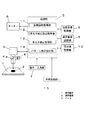
次に本発明の実施の形態を図面を参照して説明する。図1は本発明の一実施の形態のパターン認識装置の構成を示すブロック図、図2、図4は本発明の一実施の形態のパターン認識装置の操作画面を示す図、図3は本発明の一実施の形態のパターン認識方法の明るさ補正処理における輝度値変換の説明図、図5は本発明の一実施の形態のパターン認識方法の処理フロー図である。 Next, embodiments of the present invention will be described with reference to the drawings. FIG. 1 is a block diagram showing a configuration of a pattern recognition apparatus according to an embodiment of the present invention, FIGS. 2 and 4 are diagrams showing an operation screen of the pattern recognition apparatus according to an embodiment of the present invention, and FIG. FIG. 5 is an explanatory diagram of luminance value conversion in the brightness correction processing of the pattern recognition method of one embodiment, and FIG. 5 is a process flow diagram of the pattern recognition method of one embodiment of the present invention.
まず図1を参照して、パターン認識装置の構成を説明する。図1において、透明基板1はガラスなどの透明な板状部材であり、透明基板1には透明な導電体であるITO膜によって透明電極2が形成されている。透明基板1はパネル保持部(図示省略)によって保持された状態で、カメラ3の下方に位置決めされる。透明基板1の上方には照明装置4が配設されており、照明装置4とカメラ3の光軸上に配置されたハーフミラー4aによって透明基板1を上方から照明した状態でカメラ3によって透明基板1を撮像することにより、透明電極2を含む透明基板1の画像が読み取られる(図2参照)。そして読み取られた画像に対して後述するパターン認識処理を実行することにより、透明電極2のパターンが認識される。
First, the configuration of the pattern recognition apparatus will be described with reference to FIG. In FIG. 1, a
カメラ3によって撮像された画像データは処理部5に送られ、パターン認識処理の対象となる。処理部5は、画像読取処理部11、明るさ補正設定処理部12、明るさ補正処理部13、パターン検出処理部14の各処理機能部を備えている。また処理部5にはモニタ6、操作・入力部7、読取画像記憶部8、補正画像記憶部9、設定値記憶部10が付属しており、さらに、処理部5はこのパターン認識装置が組み込まれた電子部品実装装置などの外部装置の制御装置である外部制御部15に接続されている。外部制御部15からは処理部5に対してパターン認識処理の実行が指示され、処理部5から外部制御部15に対してパターン認識処理結果が出力される。
Image data picked up by the
モニタ6は表示パネルであり、カメラ3によって撮像して読み取った画像の表示や、後述する明るさ補正処理のための設定値の入力操作を行うための操作画面を表示する。操作・入力部7はキーボードやマウス、モニタ6のパネルに設けられた操作ボタンなどであり、パネル認識装置への操作入力や後述する設定値の入力操作を行う。なお、操作・入力部7をパターン認識装置に設ける替わりに、この機能を外部制御部15の操作入力機能によって行うようにしてもよい。
The
次に処理部5の処理機能を説明する。画像読取処理部11は、カメラ3によって撮像された画像の読み取り処理を行う。画像読取処理部11によって読み取られた画像は読取画像記憶部8に記憶される。明るさ補正設定処理部12は、以下に説明する明るさ補正処理部13による明るさ補正処理において用いられる設定値を設定するための処理(設定モード)を行う。後述するように、この処理はモニタ6に表示された操作画面上で行われる。
Next, the processing function of the
明るさ補正処理部13は、予め明るさ補正設定処理部12によって設定され設定値記憶部10に記憶された第1の設定値および第2の設定値に基づき、読取画像記憶部8に記憶された画像を対象として、後述する明るさ補正処理を行う。明るさ補正処理が行われた補正画像は、補正画像記憶部9に記憶される。パターン検出処理部14は、補正画像記憶部9に記憶された補正画像を対象として、透明電極のパターンを検出するパターン検出処理を行う。パターン検出結果は、外部制御部15に対して出力される。
The brightness
次に明るさ補正設定処理部12、明るさ補正処理部13によって行われる処理の内容について、モニタ6に表示される操作画面に則して説明する。図2に示す表示画面6aは、明るさ補正設定処理部12によってモニタ6に表示される操作画面を示している。表示画面6aには、画像表示フィールド20、ヒストグラム表示フィールド24、設定値入力フィールド27a、27b、入力値増減ボタン28、明るさ補正チェックボックス29が設けられている。また、マニュアル操作で明るさ補正処理部13による明るさ補正処理やパターン検出処理部14によるパターン検出処理を実行させるための操作ボタン31,32、明るさ補正設定処理部12による処理(設定モード)を終了させる終了ボタン33が設けられている。
Next, the content of the processing performed by the brightness correction setting processing unit 12 and the brightness
画像表示フィールド20にはカメラ3によって透明基板1を撮像して読み取られた読取画像20aが表示される。ヒストグラム表示フィールド24には、読取画像20aを構成する画素の輝度分布を示すヒストグラム24aが表示される。設定値入力フィールド27a、27bには、後述する第1の設定値T1、第2の設定値T2を設定するための数値が表示され、入力値増減ボタン28により数値の増減が行えるようになっている。明るさ補正チェックボックス29は、パターン認識処理(自動処理モード)において、後述する明るさ補正を実行するか否かの選択を行うために用いられ、チェックマークを付することにより、明るさ補正の実行が選択される。
In the
設定操作ボタン30を操作することにより、設定値入力フィールド27a、27bに表示された数値が第1の設定値T1、第2の設定値T2として取り込まれ設定される。操作ボタン31を操作することにより、第1の設定値T1、第2の設定値T2に基づいて明るさ補正が実行される。操作ボタン32を操作することにより、明るさ補正後の補正画像を対象としてパターン検出処理が実行され、終了ボタン33を操作することにより、設定モードを終了する。
By operating the
ここで、透明基板1を撮像した読取画像20aについて説明する。読取画像20aには、透明基板1により照明装置4の照明光が反射されて得られた背景画像21中に、同様に透明電極2により照明光が反射されて得られたパターン画像22が現れている。この読取画像20aにおいては、パターン画像22の方が背景画像21よりも高輝度の画像要素として現れるものの、これらの間には大きなコントラスト差が存在しない。そして背景画像21中にはゴミなどの非透光性の異物が暗色部分として現れた異物画像23が点在している。
Here, the
このような画像要素を含んだ読取画像20aをそのままパターン画像22を検出するためのパターンマッチングの対象とすると、読取画像20aとテンプレート画像との相互相
関を示す相関値が低下して認識エラーを生じやすい。すなわち、パターン画像22には画像ノイズが存在してパターン画像22の輝度値にはばらつきが存在する。このため前述のように背景画像21とパターン画像22とのコントラスト差が小さい場合には、この画像ノイズに起因して相関値を低下させる度合いが無視できない。さらに異物画像23は低輝度であり背景画像21との輝度差が大きいことから、異物画像23の存在により相関値はさらに低下する。そしてこれらの要因が複合すると、パターンマッチングにおけるマッチング率が低下し、認識エラーが高頻度で発生するおそれがある。
If the
このような認識エラーの発生を防止するため、本実施の形態においては、以下に説明する方法で読取画像20aに対して明るさ補正を実行し、上述の画像ノイズや異物の映像の影響を排除した補正画像を対象として、パターン検出のためのパターンマッチングを実行するようにしている。以下、この明るさ補正処理について説明する。
In order to prevent the occurrence of such a recognition error, in the present embodiment, brightness correction is performed on the read
まずヒストグラム24aについて説明する。ヒストグラム24aは、読取画像20aを構成する各画素の輝度を256階調に区分して輝度の度数分布をヒストグラムとして表示したものであり、0〜255の階調値が画素の輝度値に対応している。ヒストグラム24aには、近接した輝度値の画素に対応して度数が特定範囲の階調値に集積した梯状の度数集積部25が現れる。すなわち、図4に示すように、読取画像20aおける背景画像21、パターン画像22は、ヒストグラム24aでは高輝度範囲において比較的近接して存在する2つの度数集積部25a、25bとして現れ、また透明基板1上に存在するゴミなどの異物に対応した異物画像23は、ヒストグラム24aでは度数集積部25cとして度数集積部25bから隔たった低輝度範囲に現れる。
First, the
ヒストグラム24aには、後述する第1の設定値T1、第2の設定値T2を設定するための設定値カーソルライン26a、26bが表示されており、設定値入力フィールド27a、27bに表示される階調値(輝度値)をそれぞれ入力値増減ボタン28によって増減することにより、ヒストグラム24aにおいて設定値カーソルライン26a、26bが上下方向に移動する。そして設定操作ボタン30を操作することにより、ヒストグラム24aにおいて設定値カーソルライン26a、26bに対応する輝度値が、第1の設定値T1、第2の設定値T2として設定される。
The
明るさ補正処理においては、まず背景画像21中のパターン画像22を明瞭に識別することを目的として、ヒストグラム24aにおいて比較的近接して存在する2つの度数集積部25a、25bを確実に切り分けるための第1の設定値T1、第2の設定値T2を設定する。すなわち度数集積部25aの下限値の直下に第1の設定値T1を設定し、度数集積部25bの上限値の直上に第2の設定値T2を設定する。この設定は、図3に示す表示画面6aにおいて、入力値増減ボタン28を操作して設定値カーソルライン26a、26bを移動させることにより行われる。図3に示す例では、第1の設定値T1、第2の設定値T2はそれぞれ階調値194,168に設定されている。
In the brightness correction process, first, for the purpose of clearly identifying the
次いで設定された第1の設定値T1、第2の設定値T2に基づいて、輝度値の変換を行う。すなわち、第1の設定値T1以上の輝度値の各画素の輝度値を第1の補正値(ここでは最大階調値255)に変換するとともに、第2の設定値T2以下の輝度値の各画素の輝度値を第2の補正値(ここでは最小階調値0)に変換する。この変換処理は、処理部5に備えられたヒストグラム拡張処理機能を用いて行われる。換言すれば、ヒストグラム24aにおいて、第1の設定値T1〜第2の設定値T2の範囲を、最大階調値(255)から最小階調値(0)の範囲に拡大し、これに伴って第1の設定値T1以上の部分および第2の設定値T2以下の部分をそれぞれ圧縮したことを意味している。
Next, luminance values are converted based on the set first set value T1 and second set value T2. That is, the luminance value of each pixel having a luminance value equal to or higher than the first setting value T1 is converted into a first correction value (here, the maximum gradation value 255), and each luminance value equal to or lower than the second setting value T2 is converted. The luminance value of the pixel is converted to a second correction value (here, minimum gradation value 0). This conversion processing is performed using a histogram expansion processing function provided in the
この輝度値変換により、読取画像20aに対応したヒストグラム24aは、ヒストグラ
ム24bのような輝度分布に変化する。そしてヒストグラム24bにおいては、度数集積部25aに属していた画素の輝度値は全て一律に階調値255に変換され、また度数集積部25b、25cに属していた画素の輝度値は全て一律に階調値0に変換される。
By this luminance value conversion, the
図5は、このようにして明るさ補正が行われた後の補正画像を示している。すなわち図3に示す操作画面において、上述のように第1の設定値T1、第2の設定値T2を設定した後、操作ボタン31を操作することにより、明るさ補正処理部13による明るさ補正処理が実行され、表示画面6aの画像表示フィールド20には補正画像20bが表示される。この補正画像20bにおいては、背景画像21中にパターン画像22が明瞭なコントラストで現れており、しかも背景画像21中に点在していた異物画像23は背景画像21と同一輝度値に変換されて画像から消去された形となっている。そしてこの後、操作ボタン32を操作することにより、補正画像20bとテンプレート画像とのパターンマッチングがパターン検出処理部14によって実行され、背景画像21中のパターン画像22のパターンが検出される。
FIG. 5 shows a corrected image after the brightness correction is performed in this way. That is, on the operation screen shown in FIG. 3, after setting the first set value T1 and the second set value T2 as described above, the brightness
なお、第1の補正値、第2の補正値として、ここでは最大階調値および最小階調値を採用した例を示しているが、これ以外の値に設定してもよい。すなわち第1の補正値としては第1の設定値T1以上の輝度値、また第2の補正値としては第2の設定値T2以下の輝度値であって、輝度変換後の明るさ補正画像とテンプレート画像とをパターンマッチングした場合に、安定したマッチング結果を与える相関値が得られるような値であればよい。 In addition, although the example which employ | adopted the maximum gradation value and the minimum gradation value is shown here as a 1st correction value and a 2nd correction value, you may set to values other than this. That is, the first correction value is a luminance value that is equal to or higher than the first set value T1, and the second correction value is a luminance value that is equal to or lower than the second set value T2, and the brightness correction image after luminance conversion and Any value may be used as long as a correlation value giving a stable matching result is obtained when pattern matching is performed with the template image.
換言すれば、上述の明るさ補正処理においては、明るさ補正の対象となる画像において透明電極2に対応する画素の輝度の下限値に基づいて設定された第1の設定値T1よりも高輝度の画素の輝度値を、第1の設定値よりも高輝度に設定された第1の補正値以上の輝度値に変換し、読取画像20aにおいて透明基板1に対応した画素の輝度の上限値に基づいて設定された第2の設定値T2よりも低輝度の画素の輝度値を、第2の設定値T2よりも低輝度に設定された第2の補正値以下の輝度値に変換するようにしている。
In other words, in the brightness correction process described above, the brightness is higher than the first set value T1 set based on the lower limit value of the brightness of the pixel corresponding to the
そして、明るさ補正設定処理部12によって行われる明るさ補正設定処理においては、第1の設定値および第2の設定値の設定を、読取画像20aにおける画素の輝度分布を示すヒストグラム24aが表示された操作画面上で行うようにしている。これにより、明るさ補正を行うための設定値を、操作画面上で背景画像21と認識対象であるパターン画像22との輝度分布の相違をヒストグラム24a上で視覚的に確認しながら、適切にしかも簡便な操作で設定することが可能となっている。
In the brightness correction setting processing performed by the brightness correction setting processing unit 12, the
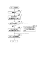
次に、パターン認識装置によって行われるパターン認識処理(自動処理モード)を、図5のフローに沿って各図を参照して説明する。パターン認識処理の実行に先立って、まず第1の設定値および第2の設定値の設定が行われる。この設定処理は、新たなワーク品種を対象とする場合に実行されるものであり、透明基板1に透明電極2が形成された実物ワークを用い、図3に示す操作画面上に、認識対象の読取画像20aを表示させて行われる。
Next, pattern recognition processing (automatic processing mode) performed by the pattern recognition apparatus will be described with reference to each drawing along the flow of FIG. Prior to the execution of the pattern recognition process, first, the first set value and the second set value are set. This setting process is executed when a new workpiece type is targeted. A real workpiece in which the
そして読取画像20aとともに表示されたヒストグラム24aにおいて背景画像21に対応した度数集積部25aとパターン画像22に対応した度数集積部25bの分布を観察し、入力値増減ボタン28を操作することにより度数集積部25aの下限値よりも低い階調値に第1の設定値T1を設定し、度数集積部25bの上限値よりも高い階調値に第2の設定値T2を設定する。
Then, in the
この後、外部制御部15よりパターン認識処理の実行が指示されると、処理部5によってパターン認識処理が実行される。まず透明基板1を撮像位置に位置決めし、透明電極2
が形成された認識対象部位をカメラ3の直下に位置させて、撮像を実行する(ST1)。次いでカメラにより撮像された画像の画像データの読み取りを実行し(画像読取処理工程)、読み取られた画像を読取画像記憶部8に記憶する(ST2)(読取画像記憶工程)。
Thereafter, when execution of pattern recognition processing is instructed by the external control unit 15, the pattern recognition processing is executed by the
The recognition target part where the is formed is positioned immediately below the
ここで、明るさ補正実行の要否(明るさ補正チェックボックス29のチェックマークの有無)を判断し(ST3)、明るさ補正を実行する場合には、明るさ補正処理部13によって前述の明るさ補正を実行する。すなわち、予め設定され記憶された第1の設定値T1および第2の設定値T2に基づき読取画像記憶部8に記憶された読取画像20a(図3)を対象として、前述の明るさ補正処理を行う(明るさ補正処理工程)。そして明るさ補正が行われた補正画像20b(図4)を補正画像記憶部9に記憶する(ST4)。また明るさ補正を実行しない場合には、読取画像記憶部8の画像データを補正画像記憶部9に転送する(ST5)。
Here, it is determined whether or not the brightness correction needs to be executed (whether or not the brightness
そして補正画像記憶部9に記憶された補正画像20bを対象として、パターン検出処理部14によって透明電極2のパターン検出処理を実行し(ST6)(パターン検出処理工程)、パターン検出結果を、外部制御部15に対して出力して、1つの認識部位を対象とした処理を終了する。
Then, the pattern detection processing unit 14 performs pattern detection processing of the
上記説明したように、本実施の形態に示すパターン認識処理は、ガラス基板などの透明基板1上に形成されたITO膜などの透明電極2を画像認識により検出するパターン認識において、パターン検出処理に先立って、明るさ補正の対象となる画像において検出対象となるパターン画像の画素の輝度の下限値に基づいて設定された第1の設定値T1よりも高輝度の画素の輝度値をより高輝度に変換し、背景画像の画素の輝度の上限値に基づいて設定された第2の設定値T2よりも低輝度の画素の輝度値をより低輝度に変換するようにしたものである。
As described above, the pattern recognition process shown in the present embodiment is a pattern detection process in pattern recognition in which a
これにより、読取画像20aにおいては背景画像21中に低コントラストで存在するパターン画像22を検出対象とする場合にあっても、パターン画像21と背景画像22とのコントラストを拡大することができる。したがって読取画像中の画像ノイズや異物の存在に起因して生じるパターンマッチングにおける相関値の低下が無く、これにより認識エラーを排除して、安定した認識を行うことができる。
As a result, even when the
本発明のパターン認識装置およびパターン認識方法は、読取画像中のゴミやノイズの影響を排除して、安定した認識を行うことができるという効果を有し、ガラス基板におけるITO膜など、明るい背景画像中に低コントラストで存在するパターンを検出するパターン認識の分野に有用である。 The pattern recognition apparatus and the pattern recognition method of the present invention have the effect of eliminating the influence of dust and noise in a read image and performing stable recognition, and a bright background image such as an ITO film on a glass substrate It is useful in the field of pattern recognition for detecting patterns existing in low contrast.
1 透明基板
2 透明電極
3 カメラ
20a 読取画像
20b 補正画像
24a、24b ヒストグラム
T1 第1の設定値
T2 第2の設定値
DESCRIPTION OF
Claims (4)
前記カメラにより撮像された画像の画像データを読み取る画像読取処理部と、前記画像読取処理部によって読み取られた画像を記憶する読取画像記憶部と、予め設定され設定値記憶部に記憶された第1の設定値および第2の設定値に基づき前記画像記憶部に記憶された画像を対象として明るさ補正処理を行う明るさ補正処理部と、明るさ補正処理が行われた補正画像を記憶する補正画像記憶部と、前記補正画像を対象として前記透明電極のパターンを検出するパターン検出処理部とを備え、
前記明るさ補正処理部は、前記明るさ補正処理の対象となる画像において前記透明電極に対応する画素の輝度の下限値に基づいて設定された前記第1の設定値よりも高輝度の画素の輝度値を前記読取画像を構成する画素の輝度値における最大階調値に変換し、前記画像において前記透明基板に対応する画素の輝度の上限値に基づいて設定された前記第2の設定値よりも低輝度の画素の輝度値を前記読取画像を構成する画素の輝度値における最小階調値に変換するヒストグラム拡張処理を実行することを特徴とするパターン認識装置。 A pattern recognition device for recognizing a pattern of the transparent electrode by capturing an image of the transparent substrate on which the transparent electrode is formed with a camera,
An image reading processing unit that reads image data of an image captured by the camera, a read image storage unit that stores an image read by the image reading processing unit, and a first preset value stored in a setting value storage unit A brightness correction processing unit that performs a brightness correction process on the image stored in the image storage unit based on the set value and the second set value, and a correction that stores the corrected image on which the brightness correction process has been performed An image storage unit, and a pattern detection processing unit that detects a pattern of the transparent electrode for the corrected image,
The brightness correction processing unit is configured to detect pixels having a luminance higher than the first set value set based on a lower limit value of the luminance of the pixel corresponding to the transparent electrode in the image subjected to the brightness correction processing. From the second set value set based on the upper limit value of the luminance of the pixel corresponding to the transparent substrate in the image, by converting the luminance value into the maximum gradation value in the luminance value of the pixel constituting the read image A pattern recognition apparatus that executes a histogram expansion process for converting a luminance value of a low-luminance pixel into a minimum gradation value in a luminance value of a pixel constituting the read image .
前記明るさ補正設定処理部は、前記ヒストグラムにおいて、前記透明電極により反射光が反射されて得られたパターン画像に対応する度数集積部の下限値に基づいて前記第1の設定値を設定し、前記透明基板により反射光が反射されて得られた背景画像に対応する度数集積部の上限値に基づいて第2の設定値を設定することを特徴とする請求項1記載のパターン認識装置。 A brightness correction setting processing unit configured to perform setting of the first setting value and the second setting value on an operation screen on which a histogram indicating a luminance distribution of pixels in the image is displayed;
The brightness correction setting processing unit sets the first setting value based on a lower limit value of a frequency accumulation unit corresponding to a pattern image obtained by reflecting reflected light by the transparent electrode in the histogram. The pattern recognition apparatus according to claim 1, wherein the second set value is set based on an upper limit value of a power accumulation unit corresponding to a background image obtained by reflecting reflected light from the transparent substrate .
前記カメラにより撮像された画像の画像データを読み取る画像読取処理工程と、前記画像読取処理工程において読み取られた画像を記憶する読取画像記憶工程と、予め設定され記憶された第1の設定値および第2の設定値に基づき前記画像記憶部に記憶された画像を対象として明るさ補正処理を行う明るさ補正処理工程と、前記明るさ補正処理が行われた補正画像を記憶する補正画像記憶工程と、前記補正画像を対象として前記透明電極のパターンを検出するパターン検出処理を行うパターン検出処理工程とを含み、
前記明るさ補正処理工程において、前記明るさ補正処理の対象となる画像において前記透明電極に対応する画素の輝度の下限値に基づいて設定された前記第1の設定値よりも高輝度の画素の輝度値を前記読取画像を構成する画素の輝度値における最大階調値に変換し、前記画像において前記透明基板に対応する画素の輝度の上限値に基づいて設定された前記第2の設定値よりも低輝度の画素の輝度値を前記読取画像を構成する画素の輝度値における最小階調値に変換するヒストグラム拡張処理を実行することを特徴とするパターン認識方法。 A pattern recognition method for recognizing a pattern of the transparent electrode by imaging a transparent substrate on which the transparent electrode is formed with a camera,
An image reading processing step for reading image data of an image captured by the camera, a read image storing step for storing an image read in the image reading processing step, a first set value and a first setting value stored in advance; A brightness correction processing step for performing brightness correction processing on the image stored in the image storage unit based on the set value of 2, and a correction image storage step for storing the correction image on which the brightness correction processing has been performed; A pattern detection processing step for performing a pattern detection process for detecting a pattern of the transparent electrode for the corrected image,
In the brightness correction processing step, pixels having higher brightness than the first set value set based on the lower limit value of the brightness of the pixel corresponding to the transparent electrode in the image subjected to brightness correction processing. From the second set value set based on the upper limit value of the luminance of the pixel corresponding to the transparent substrate in the image, by converting the luminance value into the maximum gradation value in the luminance value of the pixel constituting the read image A pattern recognition method comprising: performing a histogram expansion process for converting a luminance value of a low-luminance pixel into a minimum gradation value in a luminance value of a pixel constituting the read image .
前記ヒストグラムにおいて、前記透明電極により反射光が反射されて得られたパターン画像に対応する度数集積部の下限値に基づいて前記第1の設定値を設定し、前記透明基板により反射光が反射されて得られた背景画像に対応する度数集積部の上限値に基づいて第2の設定値を設定することを特徴とする請求項3記載のパターン認識方法。 The setting of the first setting value and the second setting value is performed on an operation screen on which a histogram indicating a luminance distribution of pixels in the image is displayed,
In the histogram, the first set value is set based on a lower limit value of the frequency accumulation unit corresponding to the pattern image obtained by reflecting the reflected light by the transparent electrode, and the reflected light is reflected by the transparent substrate. 4. The pattern recognition method according to claim 3, wherein the second set value is set based on the upper limit value of the frequency accumulating unit corresponding to the background image obtained in this way.
Priority Applications (1)
| Application Number | Priority Date | Filing Date | Title |
|---|---|---|---|
| JP2005063309A JP4635651B2 (en) | 2005-03-08 | 2005-03-08 | Pattern recognition apparatus and pattern recognition method |
Applications Claiming Priority (1)
| Application Number | Priority Date | Filing Date | Title |
|---|---|---|---|
| JP2005063309A JP4635651B2 (en) | 2005-03-08 | 2005-03-08 | Pattern recognition apparatus and pattern recognition method |
Publications (2)
| Publication Number | Publication Date |
|---|---|
| JP2006250536A JP2006250536A (en) | 2006-09-21 |
| JP4635651B2 true JP4635651B2 (en) | 2011-02-23 |
Family
ID=37091222
Family Applications (1)
| Application Number | Title | Priority Date | Filing Date |
|---|---|---|---|
| JP2005063309A Expired - Fee Related JP4635651B2 (en) | 2005-03-08 | 2005-03-08 | Pattern recognition apparatus and pattern recognition method |
Country Status (1)
| Country | Link |
|---|---|
| JP (1) | JP4635651B2 (en) |
Families Citing this family (5)
| Publication number | Priority date | Publication date | Assignee | Title |
|---|---|---|---|---|
| JP4889018B2 (en) * | 2006-11-06 | 2012-02-29 | 株式会社山武 | Appearance inspection method |
| JP5257375B2 (en) * | 2009-03-13 | 2013-08-07 | オムロン株式会社 | Image processing apparatus and image processing method |
| JP5904295B2 (en) * | 2014-03-31 | 2016-04-13 | 大日本印刷株式会社 | Colony detection system, colony detection method, and program |
| JP6286291B2 (en) * | 2014-06-19 | 2018-02-28 | 株式会社Screenホールディングス | Image processing apparatus, image acquisition apparatus, image processing method, and image acquisition method |
| WO2025032756A1 (en) * | 2023-08-09 | 2025-02-13 | 株式会社Fuji | Mounting device and component presence/absence determination method |
Family Cites Families (10)
| Publication number | Priority date | Publication date | Assignee | Title |
|---|---|---|---|---|
| JPH04343180A (en) * | 1991-05-20 | 1992-11-30 | Omron Corp | Method for displaying picture at time of setting binarizing threshold |
| JPH05256791A (en) * | 1992-03-13 | 1993-10-05 | Komatsu Ltd | Substrate defect inspection system |
| JPH07230546A (en) * | 1994-02-18 | 1995-08-29 | Mitsubishi Electric Corp | Image processing apparatus and image processing method |
| JP3424138B2 (en) * | 1994-05-11 | 2003-07-07 | カシオ計算機株式会社 | Transparent substrate alignment method |
| JPH09236487A (en) * | 1996-02-29 | 1997-09-09 | New Japan Radio Co Ltd | Method for inspecting cover tape of embossed tape |
| JP3049488B2 (en) * | 1997-04-17 | 2000-06-05 | 日本アビオニクス株式会社 | Pattern inspection method and pattern inspection device |
| JP3700577B2 (en) * | 2000-12-15 | 2005-09-28 | 株式会社島津製作所 | Foreign matter inspection device |
| JP2003196641A (en) * | 2001-12-25 | 2003-07-11 | Aisin Aw Co Ltd | Article recognition device and method |
| JP2004012422A (en) * | 2002-06-11 | 2004-01-15 | Dainippon Screen Mfg Co Ltd | Pattern inspection device, pattern inspection method, and program |
| JP4172761B2 (en) * | 2002-10-08 | 2008-10-29 | 大日本スクリーン製造株式会社 | Defect inspection apparatus, defect inspection method and program |
-
2005
- 2005-03-08 JP JP2005063309A patent/JP4635651B2/en not_active Expired - Fee Related
Also Published As
| Publication number | Publication date |
|---|---|
| JP2006250536A (en) | 2006-09-21 |
Similar Documents
| Publication | Publication Date | Title |
|---|---|---|
| US20100053348A1 (en) | Image capture device, image analysis device, external light intensity calculation method, image analysis method, image capture program, image analysis program, and storage medium | |
| CN110620887B (en) | Image generation device and image generation method | |
| JP2008170325A (en) | Spot defect detection method and spot defect detection apparatus | |
| CN111369923B (en) | Display screen outlier detection method, detection apparatus, and readable storage medium | |
| US20180332207A1 (en) | Information processing device, information processing method, and program | |
| JP2005308476A (en) | Liquid crystal display inspection apparatus and liquid crystal display inspection method | |
| JP6186465B2 (en) | Electronic display adjustment based on gaze tracking | |
| JP2009079983A (en) | Point defect detection apparatus and point defect detection method | |
| KR20140075042A (en) | Apparatus for inspecting of display panel and method thereof | |
| JP2009229197A (en) | Linear defect detecting method and device | |
| CN115330789A (en) | Screen defect detection method, device, equipment and readable storage medium | |
| JP4635651B2 (en) | Pattern recognition apparatus and pattern recognition method | |
| JP5152317B2 (en) | Presentation control apparatus and program | |
| JP2006098217A (en) | Image inspection apparatus, image inspection method, and image inspection program | |
| WO2010001973A1 (en) | Image inspection processing device, image inspection processing method, program, and recording medium | |
| JP4080514B2 (en) | Inspection device, inspection method, inspection program, and computer-readable recording medium | |
| JP2011044094A (en) | Display device | |
| JP4143660B2 (en) | Image analysis method, image analysis apparatus, inspection apparatus, image analysis program, and computer-readable recording medium | |
| JP2009115681A (en) | Image acquisition and display device | |
| JP2009060460A (en) | Optical axis adjustment value calculation device, optical axis adjustment value calculation method, optical axis adjustment value calculation program, and computer-readable recording medium | |
| JP2011029710A (en) | Image processor, image processing program, and imaging apparatus | |
| JP3408879B2 (en) | Display defect extraction method for flat panel display and apparatus therefor | |
| JP2012014558A (en) | Image processing method, image processing device, program and recording medium | |
| JP4715653B2 (en) | Laser pointer position determination system and laser pointer position determination method | |
| JP2000162089A (en) | Screen inspection method and device |
Legal Events
| Date | Code | Title | Description |
|---|---|---|---|
| A621 | Written request for application examination |
Free format text: JAPANESE INTERMEDIATE CODE: A621 Effective date: 20070125 |
|
| RD01 | Notification of change of attorney |
Free format text: JAPANESE INTERMEDIATE CODE: A7421 Effective date: 20070214 |
|
| A977 | Report on retrieval |
Free format text: JAPANESE INTERMEDIATE CODE: A971007 Effective date: 20090820 |
|
| A131 | Notification of reasons for refusal |
Free format text: JAPANESE INTERMEDIATE CODE: A131 Effective date: 20090901 |
|
| RD01 | Notification of change of attorney |
Free format text: JAPANESE INTERMEDIATE CODE: A7421 Effective date: 20091126 |
|
| A131 | Notification of reasons for refusal |
Free format text: JAPANESE INTERMEDIATE CODE: A131 Effective date: 20100413 |
|
| A521 | Request for written amendment filed |
Free format text: JAPANESE INTERMEDIATE CODE: A523 Effective date: 20100603 |
|
| TRDD | Decision of grant or rejection written | ||
| A01 | Written decision to grant a patent or to grant a registration (utility model) |
Free format text: JAPANESE INTERMEDIATE CODE: A01 Effective date: 20101026 |
|
| A01 | Written decision to grant a patent or to grant a registration (utility model) |
Free format text: JAPANESE INTERMEDIATE CODE: A01 |
|
| A61 | First payment of annual fees (during grant procedure) |
Free format text: JAPANESE INTERMEDIATE CODE: A61 Effective date: 20101108 |
|
| FPAY | Renewal fee payment (event date is renewal date of database) |
Free format text: PAYMENT UNTIL: 20131203 Year of fee payment: 3 |
|
| FPAY | Renewal fee payment (event date is renewal date of database) |
Free format text: PAYMENT UNTIL: 20131203 Year of fee payment: 3 |
|
| S111 | Request for change of ownership or part of ownership |
Free format text: JAPANESE INTERMEDIATE CODE: R313113 |
|
| R350 | Written notification of registration of transfer |
Free format text: JAPANESE INTERMEDIATE CODE: R350 |
|
| LAPS | Cancellation because of no payment of annual fees |