JP4635498B2 - Display device, control method, recording medium, and program - Google Patents
Display device, control method, recording medium, and program Download PDFInfo
- Publication number
- JP4635498B2 JP4635498B2 JP2004212986A JP2004212986A JP4635498B2 JP 4635498 B2 JP4635498 B2 JP 4635498B2 JP 2004212986 A JP2004212986 A JP 2004212986A JP 2004212986 A JP2004212986 A JP 2004212986A JP 4635498 B2 JP4635498 B2 JP 4635498B2
- Authority
- JP
- Japan
- Prior art keywords
- switch
- pixel
- display
- data
- light
- Prior art date
- Legal status (The legal status is an assumption and is not a legal conclusion. Google has not performed a legal analysis and makes no representation as to the accuracy of the status listed.)
- Expired - Fee Related
Links
Images


Classifications
-
- G—PHYSICS
- G09—EDUCATION; CRYPTOGRAPHY; DISPLAY; ADVERTISING; SEALS
- G09G—ARRANGEMENTS OR CIRCUITS FOR CONTROL OF INDICATING DEVICES USING STATIC MEANS TO PRESENT VARIABLE INFORMATION
- G09G3/00—Control arrangements or circuits, of interest only in connection with visual indicators other than cathode-ray tubes
- G09G3/20—Control arrangements or circuits, of interest only in connection with visual indicators other than cathode-ray tubes for presentation of an assembly of a number of characters, e.g. a page, by composing the assembly by combination of individual elements arranged in a matrix no fixed position being assigned to or needed to be assigned to the individual characters or partial characters
- G09G3/22—Control arrangements or circuits, of interest only in connection with visual indicators other than cathode-ray tubes for presentation of an assembly of a number of characters, e.g. a page, by composing the assembly by combination of individual elements arranged in a matrix no fixed position being assigned to or needed to be assigned to the individual characters or partial characters using controlled light sources
- G09G3/30—Control arrangements or circuits, of interest only in connection with visual indicators other than cathode-ray tubes for presentation of an assembly of a number of characters, e.g. a page, by composing the assembly by combination of individual elements arranged in a matrix no fixed position being assigned to or needed to be assigned to the individual characters or partial characters using controlled light sources using electroluminescent panels
- G09G3/32—Control arrangements or circuits, of interest only in connection with visual indicators other than cathode-ray tubes for presentation of an assembly of a number of characters, e.g. a page, by composing the assembly by combination of individual elements arranged in a matrix no fixed position being assigned to or needed to be assigned to the individual characters or partial characters using controlled light sources using electroluminescent panels semiconductive, e.g. using light-emitting diodes [LED]
- G09G3/3208—Control arrangements or circuits, of interest only in connection with visual indicators other than cathode-ray tubes for presentation of an assembly of a number of characters, e.g. a page, by composing the assembly by combination of individual elements arranged in a matrix no fixed position being assigned to or needed to be assigned to the individual characters or partial characters using controlled light sources using electroluminescent panels semiconductive, e.g. using light-emitting diodes [LED] organic, e.g. using organic light-emitting diodes [OLED]
- G09G3/3225—Control arrangements or circuits, of interest only in connection with visual indicators other than cathode-ray tubes for presentation of an assembly of a number of characters, e.g. a page, by composing the assembly by combination of individual elements arranged in a matrix no fixed position being assigned to or needed to be assigned to the individual characters or partial characters using controlled light sources using electroluminescent panels semiconductive, e.g. using light-emitting diodes [LED] organic, e.g. using organic light-emitting diodes [OLED] using an active matrix
-
- G—PHYSICS
- G09—EDUCATION; CRYPTOGRAPHY; DISPLAY; ADVERTISING; SEALS
- G09G—ARRANGEMENTS OR CIRCUITS FOR CONTROL OF INDICATING DEVICES USING STATIC MEANS TO PRESENT VARIABLE INFORMATION
- G09G2360/00—Aspects of the architecture of display systems
- G09G2360/14—Detecting light within display terminals, e.g. using a single or a plurality of photosensors
- G09G2360/141—Detecting light within display terminals, e.g. using a single or a plurality of photosensors the light conveying information used for selecting or modulating the light emitting or modulating element
- G09G2360/142—Detecting light within display terminals, e.g. using a single or a plurality of photosensors the light conveying information used for selecting or modulating the light emitting or modulating element the light being detected by light detection means within each pixel
Landscapes
- Engineering & Computer Science (AREA)
- Physics & Mathematics (AREA)
- Computer Hardware Design (AREA)
- General Physics & Mathematics (AREA)
- Theoretical Computer Science (AREA)
- Electroluminescent Light Sources (AREA)
- Control Of Indicators Other Than Cathode Ray Tubes (AREA)
- Devices For Indicating Variable Information By Combining Individual Elements (AREA)
- Control Of El Displays (AREA)
Description
本発明は、表示装置、制御方法、記録媒体、およびプログラムに関し、特に、外部から照射された光に対する検出感度を向上させることができるようにする表示装置、制御方法、記録媒体、およびプログラムに関する。 The present invention relates to a display device, a control method, a recording medium, and a program, and more particularly, to a display device, a control method, a recording medium, and a program that can improve detection sensitivity to light emitted from the outside.
近年、タッチパネルなどを重畳して設けることなく、表示装置に対して各種の情報を直接入力することができる技術が各種提案されている(特許文献1,2)。
In recent years, various techniques for directly inputting various types of information to a display device without providing a touch panel or the like have been proposed (
例えば、特許文献2には、印加する電圧を制御することによって、それぞれの画素に、画像を表示する動作である発光動作と、外部からの光を検出する動作である受光動作を行わせることができるディスプレイが開示されている。このディスプレイにおいては、受光動作の際、発光動作のときと逆方向の電圧が印加され、そのような逆方向の電圧が印加された状態で光が照射されたときに画素内で発生されるリーク電流を用いて外部からの光が検出される。これにより、ユーザは、所定のデータを表す光をディスプレイに照射することによって、そのデータをディスプレイに直接入力することができる。
For example, in
同様に、外部からの光に応じた所定の動作を行うものとして、特許文献3には、光応答性を有する膜を用い、光入力に応じた発光表示が行われるようにした発光表示素子が、特許文献4には、ストライプ状の電極群を直交させ、その交点にアモルファスシリコンの層を挟み込むことによって、各交点に光電池を配置するようにした装置がそれぞれ開示されている。
Similarly, as a device that performs a predetermined operation according to light from the outside, Patent Document 3 discloses a light-emitting display element that uses a film having photoresponsiveness to perform light-emitting display according to light input.
また、特許文献5には、発光素子である有機EL素子により、光入力された情報を検出させる技術が開示されている。
ところで、例えば、特許文献2に開示されているディスプレイのように、画素で発生されたリーク電流を用いることによって外部からの光の有無を検出する装置においては、単位面積に含まれる画素を照射した光の量(エネルギー)によって検出感度が定まる。
By the way, for example, in a device that detects the presence or absence of light from the outside by using a leak current generated in a pixel, such as a display disclosed in
すなわち、十分の量の光が照射された場合には、それに応じて十分な量のリーク電流が発生されるから検出感度が高まり、少ない量の光が照射された場合には、それに応じて少ない量のリーク電流が発生されるから検出感度が低くなる。 That is, when a sufficient amount of light is irradiated, a sufficient amount of leakage current is generated accordingly, so that the detection sensitivity is increased, and when a small amount of light is irradiated, the amount is decreased accordingly. Since a large amount of leakage current is generated, the detection sensitivity is lowered.
このように、照射された光の量によって検出感度が定まることから、光の量が多い場合には問題ないものの、照射された光の量が少ない場合には、外部からの入力を正しく検出させることができないおそれがあり、問題である。 In this way, the detection sensitivity is determined by the amount of irradiated light, so there is no problem when the amount of light is large, but when the amount of irradiated light is small, the input from the outside is correctly detected. This is a problem.
このことは、外部からの光の入力に応じて所定の動作を行う、他の文献に開示されている素子や装置などにも共通することである。 This is also common to elements and devices disclosed in other documents that perform a predetermined operation in response to external light input.
本発明はこのような状況に鑑みてなされたものであり、外部から照射された光に対する検出感度を向上させることができるようにするものである。 The present invention has been made in view of such a situation, and makes it possible to improve detection sensitivity with respect to light irradiated from the outside.
本発明の表示装置は、EL素子と、前記EL素子と並列に設けられる容量と、表示データを表す信号の伝送に用いられる表示データ信号線に接続されるとともに、発光動作を行わせる画素の選択に用いられる表示ライン選択線を介して導通/非導通が制御される第1のスイッチと、前記EL素子のアノード電極と前記第1のスイッチの間に設けられる第2のスイッチと、前記EL素子のアノード電極に接続され、受光動作を行わせる画素の選択に用いられる読み出しライン選択線を介して導通/非導通が制御される第3のスイッチと、前記EL素子のアノード電極と前記容量の間に設けられる第4のスイッチと、前記第3のスイッチを介して供給された信号をデータに変換し、前記データの伝送に用いられる受光データ信号線に出力する変換回路とが各画素に配置されたディスプレイと、前記ディスプレイの画素の前記第1乃至第4のスイッチが非導通の状態において、所定の画素に発光動作を行わせる場合、発光動作を行わせる画素を、前記表示ライン選択線を介して前記第1のスイッチを導通状態として前記表示データを表す信号を導通させ、前記第1のスイッチを非導通状態とした後、前記第2のスイッチを導通状態として、前記第2のスイッチを介して前記表示データを表す信号を前記EL素子に供給させて前記EL素子を発光させるように制御し、発光動作を行っていた画素に受光動作を行わせる場合、受光動作を行わせる画素を、前記第4のスイッチを導通状態、前記第2のスイッチを非導通状態とし、光が照射されることに応じて前記EL素子が発生した電荷を前記第4のスイッチを介して前記容量に蓄積させ、所定の期間経過後に、前記読み出しライン選択線を介して前記第3のスイッチを導通状態とし、前記容量に蓄積させた電荷を前記第4のスイッチと前記第3のスイッチを介して前記変換回路に供給させ、前記変換回路から前記データを出力させるように制御する制御手段と、受光動作を行っていた画素から前記受光データ信号線を介して供給された前記データを検出する検出手段とを備える。 The display device of the present invention is connected to an EL element, a capacitor provided in parallel with the EL element, and a display data signal line used for transmission of a signal representing display data, and selection of a pixel for performing a light emitting operation A first switch whose conduction / non-conduction is controlled via a display line selection line used for the display, a second switch provided between the anode electrode of the EL element and the first switch, and the EL element A third switch connected to the anode electrode of the EL element and controlled to be conductive / non-conductive through a read line selection line used to select a pixel for performing a light receiving operation, and between the anode electrode of the EL element and the capacitor And a conversion circuit that converts a signal supplied via the third switch into data and outputs the data to a light reception data signal line used for transmission of the data. When a predetermined pixel is caused to perform a light emission operation in a state where the display arranged in the display and the first to fourth switches of the display pixel are non-conductive, the pixel for performing the light emission operation is selected as the display line. The signal representing the display data is turned on by setting the first switch to a conductive state via a line, the first switch is turned off, and then the second switch is turned on. A pixel that performs a light receiving operation when a signal that represents the display data is supplied to the EL element via a switch and the EL element is controlled to emit light and the light emitting operation is performed on the pixel that has performed the light emitting operation. The fourth switch is turned on, the second switch is turned off, and the charge generated by the EL element in response to light irradiation is transmitted through the fourth switch. After the predetermined period has elapsed, the third switch is turned on via the read line selection line, and the charge accumulated in the capacitor is transferred to the fourth switch and the third switch. A control means for controlling to supply the data to the conversion circuit and outputting the data from the conversion circuit; and detecting the data supplied via the light reception data signal line from a pixel that has performed a light reception operation. Detecting means.
前記容量は、前記EL素子と並列に設けられる寄生容量とは異なる容量であるようにすることができる。 The capacitance may be different from a parasitic capacitance provided in parallel with the EL element.
本発明の制御方法は、EL素子と、前記EL素子と並列に設けられる容量と、表示データを表す信号の伝送に用いられる表示データ信号線に接続されるとともに、発光動作を行わせる画素の選択に用いられる表示ライン選択線を介して導通/非導通が制御される第1のスイッチと、前記EL素子のアノード電極と前記第1のスイッチの間に設けられる第2のスイッチと、前記EL素子のアノード電極に接続され、受光動作を行わせる画素の選択に用いられる読み出しライン選択線を介して導通/非導通が制御される第3のスイッチと、前記EL素子のアノード電極と前記容量の間に設けられる第4のスイッチと、前記第3のスイッチを介して供給された信号をデータに変換し、前記データの伝送に用いられる受光データ信号線に出力する変換回路とが各画素に配置されたディスプレイを備える表示装置の制御方法において、前記ディスプレイの画素の前記第1乃至第4のスイッチが非導通の状態において、所定の画素に発光動作を行わせる場合、発光動作を行わせる画素を、前記表示ライン選択線を介して前記第1のスイッチを導通状態として前記表示データを表す信号を導通させ、前記第1のスイッチを非導通状態とした後、前記第2のスイッチを導通状態として、前記第2のスイッチを介して前記表示データを表す信号を前記EL素子に供給させて前記EL素子を発光させるように制御し、発光動作を行っていた画素に受光動作を行わせる場合、受光動作を行わせる画素を、前記第4のスイッチを導通状態、前記第2のスイッチを非導通状態とし、光が照射されることに応じて前記EL素子が発生した電荷を前記第4のスイッチを介して前記容量に蓄積させ、所定の期間経過後に、前記読み出しライン選択線を介して前記第3のスイッチを導通状態とし、前記容量に蓄積させた電荷を前記第4のスイッチと前記第3のスイッチを介して前記変換回路に供給させ、前記変換回路から前記データを出力させるように制御し、受光動作を行っていた画素から前記受光データ信号線を介して供給された前記データを検出するステップを含む。
According to the control method of the present invention, an EL element, a capacitor provided in parallel with the EL element, a display data signal line used for transmission of a signal representing display data, and a pixel for performing a light emitting operation are selected. A first switch whose conduction / non-conduction is controlled via a display line selection line used for the display, a second switch provided between the anode electrode of the EL element and the first switch, and the EL element A third switch connected to the anode electrode of the EL element and controlled to be conductive / non-conductive through a read line selection line used to select a pixel for performing a light receiving operation, and between the anode electrode of the EL element and the capacitor And a conversion circuit that converts a signal supplied via the third switch into data and outputs the data to a light reception data signal line used for transmission of the data. In the control method of the display device including the display disposed in the display device, when the first pixel to the fourth switch of the pixel of the display are in a non-conductive state, the light emitting operation is performed when the predetermined pixel performs the light emitting operation. The pixel makes the first switch conductive through the display line selection line to conduct a signal representing the display data, and the first switch is made non-conductive, and then the second switch is made conductive. A state where a signal representing the display data is supplied to the EL element through the second switch to control the EL element to emit light, and the pixel that has performed the light emitting operation performs the light receiving operation. The EL element is generated in response to the irradiation of light with the pixel that performs the light receiving operation in which the fourth switch is turned on and the second switch is turned off. Charge is accumulated in the capacitor via the fourth switch, and after a predetermined period, the third switch is turned on via the read line selection line, and the charge accumulated in the capacitor is 4 is supplied to the conversion circuit via the
本発明の記録媒体は、EL素子と、前記EL素子と並列に設けられる容量と、表示データを表す信号の伝送に用いられる表示データ信号線に接続されるとともに、発光動作を行わせる画素の選択に用いられる表示ライン選択線を介して導通/非導通が制御される第1のスイッチと、前記EL素子のアノード電極と前記第1のスイッチの間に設けられる第2のスイッチと、前記EL素子のアノード電極に接続され、受光動作を行わせる画素の選択に用いられる読み出しライン選択線を介して導通/非導通が制御される第3のスイッチと、前記EL素子のアノード電極と前記容量の間に設けられる第4のスイッチと、前記第3のスイッチを介して供給された信号をデータに変換し、前記データの伝送に用いられる受光データ信号線に出力する変換回路とが各画素に配置されたディスプレイを備える表示装置を制御するコンピュータに実行させるプログラムが記録された記録媒体において、前記ディスプレイの画素の前記第1乃至第4のスイッチが非導通の状態において、所定の画素に発光動作を行わせる場合、発光動作を行わせる画素を、前記表示ライン選択線を介して前記第1のスイッチを導通状態として前記表示データを表す信号を導通させ、前記第1のスイッチを非導通状態とした後、前記第2のスイッチを導通状態として、前記第2のスイッチを介して前記表示データを表す信号を前記EL素子に供給させて前記EL素子を発光させるように制御し、発光動作を行っていた画素に受光動作を行わせる場合、受光動作を行わせる画素を、前記第4のスイッチを導通状態、前記第2のスイッチを非導通状態とし、光が照射されることに応じて前記EL素子が発生した電荷を前記第4のスイッチを介して前記容量に蓄積させ、所定の期間経過後に、前記読み出しライン選択線を介して前記第3のスイッチを導通状態とし、前記容量に蓄積させた電荷を前記第4のスイッチと前記第3のスイッチを介して前記変換回路に供給させ、前記変換回路から前記データを出力させるように制御し、受光動作を行っていた画素から前記受光データ信号線を介して供給された前記データを検出するステップを含む処理をコンピュータに実行させるプログラムが記録された記録媒体である。 The recording medium of the present invention includes an EL element, a capacitor provided in parallel with the EL element, a display data signal line used for transmission of a signal representing display data, and a pixel for performing a light emitting operation. A first switch whose conduction / non-conduction is controlled via a display line selection line used for the display, a second switch provided between the anode electrode of the EL element and the first switch, and the EL element A third switch connected to the anode electrode of the EL element and controlled to be conductive / non-conductive through a read line selection line used to select a pixel for performing a light receiving operation, and between the anode electrode of the EL element and the capacitor And a conversion circuit that converts a signal supplied via the third switch into data and outputs the data to a light reception data signal line used for transmission of the data. In a recording medium on which is recorded a program to be executed by a computer that controls a display device including a display arranged on the display device, light is emitted to a predetermined pixel when the first to fourth switches of the display pixel are non-conductive When the operation is performed, the pixel that performs the light emitting operation causes the signal representing the display data to be turned on by setting the first switch to the conductive state via the display line selection line, and the first switch is turned off. After that, the second switch is turned on, and a signal representing the display data is supplied to the EL element through the second switch so that the EL element emits light, and the light emitting operation is performed. When the light receiving operation is performed on the pixel that has been performed, the fourth switch is turned on and the second switch is turned off for the pixel that performs the light receiving operation. The charge generated by the EL element in response to light irradiation is accumulated in the capacitor via the fourth switch, and after a predetermined period has elapsed, the charge is generated via the read line selection line. 3 is turned on, and the charge accumulated in the capacitor is supplied to the conversion circuit via the fourth switch and the third switch, and the data is output from the conversion circuit. A recording medium on which a program for causing a computer to execute a process including a step of detecting the data supplied from the pixel that has been performing the light receiving operation via the light receiving data signal line is recorded.
本発明のプログラムは、EL素子と、前記EL素子と並列に設けられる容量と、表示データを表す信号の伝送に用いられる表示データ信号線に接続されるとともに、発光動作を行わせる画素の選択に用いられる表示ライン選択線を介して導通/非導通が制御される第1のスイッチと、前記EL素子のアノード電極と前記第1のスイッチの間に設けられる第2のスイッチと、前記EL素子のアノード電極に接続され、受光動作を行わせる画素の選択に用いられる読み出しライン選択線を介して導通/非導通が制御される第3のスイッチと、前記EL素子のアノード電極と前記容量の間に設けられる第4のスイッチと、前記第3のスイッチを介して供給された信号をデータに変換し、前記データの伝送に用いられる受光データ信号線に出力する変換回路とが各画素に配置されたディスプレイを備える表示装置を制御するコンピュータに実行させるプログラムにおいて、前記ディスプレイの画素の前記第1乃至第4のスイッチが非導通の状態において、所定の画素に発光動作を行わせる場合、発光動作を行わせる画素を、前記表示ライン選択線を介して前記第1のスイッチを導通状態として前記表示データを表す信号を導通させ、前記第1のスイッチを非導通状態とした後、前記第2のスイッチを導通状態として、前記第2のスイッチを介して前記表示データを表す信号を前記EL素子に供給させて前記EL素子を発光させるように制御し、発光動作を行っていた画素に受光動作を行わせる場合、受光動作を行わせる画素を、前記第4のスイッチを導通状態、前記第2のスイッチを非導通状態とし、光が照射されることに応じて前記EL素子が発生した電荷を前記第4のスイッチを介して前記容量に蓄積させ、所定の期間経過後に、前記読み出しライン選択線を介して前記第3のスイッチを導通状態とし、前記容量に蓄積させた電荷を前記第4のスイッチと前記第3のスイッチを介して前記変換回路に供給させ、前記変換回路から前記データを出力させるように制御し、受光動作を行っていた画素から前記受光データ信号線を介して供給された前記データを検出するステップを含む処理をコンピュータに実行させる。 The program of the present invention is used to select an EL element, a capacitor provided in parallel with the EL element, a display data signal line used for transmission of a signal representing display data, and a pixel for performing a light emitting operation. A first switch whose conduction / non-conduction is controlled via a display line selection line used; a second switch provided between the anode electrode of the EL element and the first switch; A third switch connected to the anode electrode and controlled to be conductive / non-conductive through a read line selection line used for selecting a pixel for performing a light receiving operation; and between the anode electrode of the EL element and the capacitor. A fourth switch provided; and a conversion circuit that converts a signal supplied via the third switch into data and outputs the data to a light reception data signal line used for transmission of the data. In a program that is executed by a computer that controls a display device that includes a display that is arranged in a raw manner, when a first pixel to a fourth switch of a pixel of the display are in a non-conductive state, a predetermined pixel performs a light emitting operation The pixel that performs the light emitting operation is made to conduct the signal representing the display data through the display line selection line by setting the first switch to the conductive state, and the first switch to the non-conductive state. The second switch is turned on, and a signal representing the display data is supplied to the EL element through the second switch so that the EL element emits light. When the light receiving operation is performed, the pixel that performs the light receiving operation is turned on by turning on the fourth switch and turning off the second switch. In response to this, the charge generated by the EL element is accumulated in the capacitor via the fourth switch, and after a predetermined period, the third switch is turned on via the read line selection line. The charge accumulated in the capacitor is supplied to the conversion circuit via the fourth switch and the third switch, and the data is output from the conversion circuit to perform the light receiving operation. A computer is caused to execute processing including a step of detecting the data supplied from a pixel via the light reception data signal line.
本発明においては、ディスプレイの画素の第1乃至第4のスイッチが非導通の状態において、所定の画素に発光動作を行わせる場合、発光動作を行わせる画素が、表示ライン選択線を介して前記第1のスイッチを導通状態として表示データを表す信号を導通させ、前記第1のスイッチを非導通状態とした後、前記第2のスイッチを導通状態として、前記第2のスイッチを介して前記表示データを表す信号をEL素子に供給させて前記EL素子を発光させるように制御される。また、発光動作を行っていた画素に受光動作を行わせる場合、受光動作を行わせる画素が、前記第4のスイッチを導通状態、前記第2のスイッチを非導通状態とし、光が照射されることに応じて前記EL素子が発生した電荷を前記第4のスイッチを介して容量に蓄積させ、所定の期間経過後に、前記読み出しライン選択線を介して前記第3のスイッチを導通状態とし、前記容量に蓄積させた電荷を前記第4のスイッチと前記第3のスイッチを介して前記変換回路に供給させ、前記変換回路から前記データを出力させるように制御される。さらに、受光動作を行っていた画素から受光データ信号線を介して供給された前記データが検出される。 In the present invention, when a predetermined pixel performs a light emission operation in a state where the first to fourth switches of the display pixels are non-conductive, the pixel performing the light emission operation is connected to the pixel via the display line selection line. A signal representing display data is turned on by turning on the first switch, the first switch is turned off, and then the second switch is turned on and the display is made via the second switch. The EL element is controlled to emit light by supplying a signal representing data to the EL element. In addition, when a light receiving operation is performed on a pixel that has performed a light emitting operation, the pixel that performs the light receiving operation sets the fourth switch to a conductive state and the second switch to a nonconductive state, and is irradiated with light. Accordingly, the charge generated by the EL element is accumulated in a capacitor via the fourth switch, and after a predetermined period, the third switch is turned on via the read line selection line, Control is performed such that the charge accumulated in the capacitor is supplied to the conversion circuit via the fourth switch and the third switch, and the data is output from the conversion circuit. Further, the data supplied from the pixel that has been performing the light receiving operation via the light receiving data signal line is detected.
本発明によれば、画像の表示と、外部からの光の検出が可能になる。 According to the present invention, it is possible to display an image and detect light from the outside.
また、本発明によれば、外部からの光に対する検出感度を向上させることができる。 In addition, according to the present invention, it is possible to improve the detection sensitivity for light from the outside.
以下、本発明の実施の形態について図を参照して説明する。 Hereinafter, embodiments of the present invention will be described with reference to the drawings.
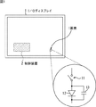
図1は、本発明を適用したI/O(IN/OUT)ディスプレイ1の外観の例を示す図である。
FIG. 1 is a diagram showing an example of the appearance of an I / O (IN / OUT)
I/Oディスプレイ1は、それを構成する各画素により、外部から照射された光を検出するIN機能(検出機能)と、所定の画像を表示するOUT機能(表示機能)を実現可能なディスプレイである。
The I /
図1の円の中に拡大して示すように、I/Oディスプレイ1を構成する各画素は、例えば、TFT(Thin Film Transistor)よりなるスイッチ11、有機または無機のEL素子12、EL素子12に寄生する容量である寄生容量13で表される。すなわち、I/Oディスプレイ1は、アクティブマトリクス駆動が可能な自発光型のELディスプレイである。
As shown in an enlarged circle in FIG. 1, each pixel constituting the I /
I/Oディスプレイ1においては、その各画素の動作が制御装置2により制御され、IN機能とOUT機能が実現される。
In the I /
ここで、IN機能とOUT機能について説明する。 Here, the IN function and the OUT function will be described.
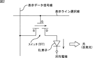
図2および図3は、I/Oディスプレイ1の1画素に相当する回路の例を示す図である。
2 and 3 are diagrams illustrating examples of circuits corresponding to one pixel of the I /
表示ライン選択線(ゲート線)によりTFTのゲート電極Gに正方向の電圧(バイアス)が印加されたとき、図2の実線矢印で示すように、表示データ信号線(ソース線)によりソース電極Sに印加された電圧に応じて、アモルファスシリコンやポリシリコンからなる活性半導体層(チャネル)中をソース電極Sからドレイン電極D方向に電流が流れる。 When a positive voltage (bias) is applied to the TFT gate electrode G by the display line selection line (gate line), as shown by the solid line arrow in FIG. 2, the display data signal line (source line) causes the source electrode S. A current flows in the direction from the source electrode S to the drain electrode D in an active semiconductor layer (channel) made of amorphous silicon or polysilicon in accordance with the voltage applied to the first electrode.
TFTのドレイン電極DにはEL素子のアノード電極が接続されており、TFTのチャネル中を電流が流れることにより生じるアノード−カソード電極間の電位差に応じて、図2の白抜き矢印で示すようにEL素子が発光する。 The anode electrode of the EL element is connected to the drain electrode D of the TFT, and as shown by the white arrow in FIG. 2 according to the potential difference between the anode and the cathode electrode caused by the current flowing in the TFT channel. The EL element emits light.
EL素子からの光はディスプレイの外部に出射される。従って、このような画素の動作により画像の表示、すなわち、OUT機能が実現される。 Light from the EL element is emitted outside the display. Therefore, the display of an image, that is, the OUT function is realized by the operation of such a pixel.
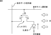
一方、TFTのゲート電極Gに0V近傍かまたは逆方向の電圧が表示ライン選択線により印加された場合、ソース電極Sに表示データ信号線により電圧が印加されているときでもチャネル中を電流が流れず、EL素子のアノード−カソード電極間には電位差が生じないから発光しない。 On the other hand, when a voltage in the vicinity of 0V or in the reverse direction is applied to the TFT gate electrode G by the display line selection line, a current flows through the channel even when a voltage is applied to the source electrode S by the display data signal line. In addition, since no potential difference is generated between the anode and the cathode of the EL element, no light is emitted.
この状態で、外部からの光が白抜き矢印で示すように図3の画素を照射したとき、TFTのチャネルの光伝導性によりゲート電極Gが開き(チャネルができ)、微量ではあるがドレイン電極Dからソース電極S方向にリーク電流(オフ電流)が流れる。また、EL素子においては、リーク電流が発生される。 In this state, when light from the outside irradiates the pixel of FIG. 3 as indicated by a white arrow, the gate electrode G is opened due to the photoconductivity of the TFT channel (a channel is formed), and a small amount of the drain electrode A leakage current (off-state current) flows from D to the source electrode S direction. In addition, a leak current is generated in the EL element.
このことから、0V近傍かまたは逆方向の電圧を印加した画素(TFT、EL素子)を流れるリーク電流を増幅してその有無を検出することによって、画素に対して外部から光が照射されたのか否かを識別することが可能になる。また、リーク電流の量によって、光の量も識別することが可能になる。すなわち、これによりIN機能が実現される。 From this, whether the pixel was exposed to light from outside by amplifying the leakage current flowing through the pixel (TFT, EL element) applied with a voltage in the vicinity of 0 V or in the reverse direction and detecting its presence or absence It becomes possible to identify whether or not. Further, the amount of light can be identified by the amount of leakage current. That is, the IN function is realized by this.
例えば、ユーザは、このような画素からなるディスプレイに所定のデータを表す光を当てることによって、当てた光をディスプレイに検出させることができ、光を介してデータを入力することができる。 For example, the user can cause the display to detect the applied light by applying light representing predetermined data to the display including such pixels, and can input the data through the light.
以下、図2に示すように正方向の電圧が印可されたときの画素(EL素子)の動作を発光動作と、図3に示すように、逆方向の電圧が印可され、外部から照射された光に応じてリーク電流を発生する画素の動作を受光動作という。 Hereinafter, the operation of the pixel (EL element) when a positive voltage is applied as shown in FIG. 2 and the light emission operation as shown in FIG. 3, and a reverse voltage is applied and irradiated from the outside as shown in FIG. The operation of a pixel that generates a leak current in response to light is called a light receiving operation.
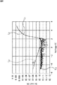
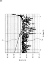
図4は、図2および図3に示す画素の電流特性を示す図である。縦軸は画素中の電流の値を表し、横軸はゲート電極Gに印加された電圧の値を表す。 FIG. 4 is a diagram showing current characteristics of the pixels shown in FIGS. The vertical axis represents the value of the current in the pixel, and the horizontal axis represents the value of the voltage applied to the gate electrode G.
計測結果を表す線L1は、正方向の電圧が印加された状態で光が照射されたときに画素で検出される電流(TFTのチャネル中を流れる電流と、EL素子が発生する電流)の値を表しており、線L2は、正方向の電圧が印加された状態で光が照射されていないときに画素で検出される電流の値を表している。 The line L 1 representing the measurement result is a current detected by the pixel when light is irradiated with a positive voltage applied (current flowing in the TFT channel and current generated by the EL element). represents a value, the line L 2 represents the value of the current light in a state where the forward voltage is applied is detected by the pixel when not irradiated.
この線L1およびL2により、正方向の電圧が印加されている場合は、外部からの光の有無に関わらず、検出される電流値には差がみられないことがわかる。 It can be seen from these lines L 1 and L 2 that when a positive voltage is applied, there is no difference in the detected current value regardless of the presence or absence of light from the outside.
一方、図4の線L3は、逆方向の電圧が印加されている状態で外部から光が照射されたときに、その画素で検出された電流の値を表しており、線L4は、逆方向の電圧が印加されている状態で外部から光が照射されていないときに、その画素で検出された電流の値を表している。 On the other hand, the line L 3 in FIG. 4, when the external light is irradiated in a state in which a reverse voltage is applied, which represents the value of the current detected by the pixel, the line L 4 are, The value of the current detected in the pixel when light is not irradiated from the outside in a state where a reverse voltage is applied is shown.
線L3と線L4を比較してわかるように、逆方向の電圧が印加されている場合、外部から光が照射されたときと、照射されていないときとで、その画素で検出される電流に差が生じている。例えば、約−5ボルトの電圧(逆方向の電圧)が印加されている状態において、外部から所定の光量の光が照射された場合、「1E−8(A)」程度の電流(TFTの活性半導体層中を流れる電流と、EL素子により発生された電流)が検出される。 As can be seen by comparing line L 3 and line L 4 , when a reverse voltage is applied, the pixel is detected when light is irradiated from the outside and when it is not irradiated. There is a difference in current. For example, when a predetermined amount of light is applied from the outside in a state where a voltage of about −5 volts (reverse voltage) is applied, a current of about “1E-8 (A)” (the TFT activity) Current flowing in the semiconductor layer and current generated by the EL element) are detected.
図4においては、外部から光が照射されていない場合であっても、「1E−10(A)」程度の微小な電流が発生していることが線L4により示されているが、これは計測中のノイズによるものである。なお、RGBのうちのいずれの色を発光するEL素子の画素であっても、図4に示すものとほぼ同様の計測結果が得られる。 In FIG. 4, the line L 4 indicates that a minute current of about “1E-10 (A)” is generated even when light is not irradiated from the outside. Is due to noise during measurement. Note that the measurement result almost the same as that shown in FIG. 4 can be obtained for any pixel of the EL element that emits any color of RGB.
図5は、図4の0V近傍を拡大して示す図である。 FIG. 5 is an enlarged view showing the vicinity of 0V in FIG.
図5の線L3と線L4により示されるように、0V近傍の電圧が印加されている状態でも、光が照射されている場合と、照射されていない場合とで、その電流値に差が検出される。 As shown by the lines L 3 and L 4 in FIG. 5, even when a voltage near 0 V is applied, there is a difference in the current value between when light is irradiated and when it is not irradiated. Is detected.
従って、0V近傍の電圧を印加している状態でも、発生した電流を増幅させることで、この差、すなわち、光が照射されているか否かの検出が可能となる。 Therefore, even when a voltage in the vicinity of 0 V is applied, it is possible to detect this difference, that is, whether or not light is irradiated, by amplifying the generated current.
このことから、積極的に逆方向の電圧を印加することなく、ゲート電圧が0V近傍の値になるように制御することで、ある画素に受光動作を行わせることができる。 Therefore, it is possible to cause a certain pixel to perform a light receiving operation by controlling the gate voltage to be a value in the vicinity of 0 V without actively applying a reverse voltage.
ゲート電圧が0V近傍の値になるように制御して受光動作を行わせることにより、逆方向の電圧を印加してその動作を行わせる場合に較べて、逆方向の電圧の分だけ消費電力を抑えることができる。 By controlling the gate voltage to be a value near 0V and performing the light receiving operation, the power consumption is reduced by the amount of the reverse voltage compared to applying the reverse voltage and performing the operation. Can be suppressed.
また、制御する電圧の数が少なくなるため、その制御、さらにはシステム構成が容易になる。すなわち、ゲート電圧が0V近傍の値になるように制御することは、正方向の電圧が印加されないように制御することでもあるから、正方向の電圧が印加されるようにゲート電圧を制御する制御線や電源回路だけをもって実現することができる(逆方向の電圧が印加されるようにゲート電圧を制御する制御線を別に設ける必要がない)。 Further, since the number of voltages to be controlled is reduced, the control and the system configuration are facilitated. In other words, the control to control the gate voltage so that the positive voltage is applied since the control so that the gate voltage becomes a value near 0V is also the control so that the positive voltage is not applied. It can be realized with only a line and a power supply circuit (there is no need to provide a separate control line for controlling the gate voltage so that a reverse voltage is applied).
これにより、ディスプレイの駆動基板やシステム基板上の電源回路の構成を簡略化することができ、低消費電力化を実現することができるだけでなく、基板上の限られたスペースの効率的な利用も実現することができる。 This simplifies the configuration of the power supply circuit on the display drive board and system board, and not only lowers power consumption, but also makes efficient use of limited space on the board. Can be realized.
さらに、逆方向の電圧を印加しないようにすることにより、逆方向の電圧を印加したときに生じることのあるTFTやEL素子の破壊を回避することができる。例えば、チャネル長(L長)を長くすることでTFTの耐電圧性を高めることができるが、この場合、導通時の電流が下がってしまい、十分な電流を確保するためには、チャネル幅(W長)を大きくする必要がある。 Further, by not applying the reverse voltage, it is possible to avoid the breakdown of the TFT or EL element that may occur when the reverse voltage is applied. For example, the withstand voltage of the TFT can be increased by increasing the channel length (L length). However, in this case, the current during conduction decreases, and the channel width ( W length) needs to be increased.
この結果、TFTを流れる電流値を変えることなく耐電圧性を高めるためには、1つのTFTのサイズを大きくする必要があり、各画素のサイズが小さい高精細なディスプレイの各画素に、そのTFTを配置することが困難となる。 As a result, in order to increase the withstand voltage without changing the current value flowing through the TFT, it is necessary to increase the size of one TFT, and each TFT of a high-definition display with a small size of each pixel has its TFT. It becomes difficult to arrange.
従って、逆方向の電圧をなくすことで、TFTやEL素子の耐圧設計が容易になり、かつ、TFTやEL素子そのもののサイズを小さくすることができ、これにより、高精細なディスプレイを実現することが可能になる。 Therefore, by eliminating the reverse voltage, the withstand voltage design of the TFT and EL elements can be facilitated, and the size of the TFT and EL elements themselves can be reduced, thereby realizing a high-definition display. Is possible.
以上のように、各画素にTFTとEL素子が設けられているI/Oディスプレイ1によっては、画像の表示だけでなく、0V近傍か、それより逆方向の電圧を印加することによって、画素を用いて外部からの光を検出させることが可能になる。
As described above, depending on the I /
ところで、このように発光動作だけでなく受光動作が可能な画素からなるディスプレイにおいては、受光動作を行っている画素を照射する光の量(エネルギー)によって、EL素子の光電効果により発生されるリーク電流の量が異なる。 By the way, in such a display composed of pixels that can perform not only light emission operation but also light reception operation, leakage caused by the photoelectric effect of the EL element is caused by the amount (energy) of light irradiating the pixel performing light reception operation. The amount of current is different.
従って、照射する光の量が多い程、発生されるリーク電流の量が多くなることから、受光感度は上がり、一方、照射する光の量が少ない程、発生されるリーク電流の量が少なくなることから、受光感度は下がることになる。 Accordingly, the greater the amount of light that is emitted, the greater the amount of leak current that is generated, so the light receiving sensitivity is increased. On the other hand, the smaller the amount of light that is irradiated, the smaller the amount of leak current that is generated. Therefore, the light receiving sensitivity is lowered.
そこで、図1のI/Oディスプレイ1においては、受光動作を行っている画素が外部からの光を受けることに応じて発生した電荷を所定の期間だけ所定の容量に蓄積させておき、蓄積させておいた電荷の量(電流の量)をまとめて検出することにより、受光感度を上げるようになされている。
Therefore, in the I /
すなわち、光を受けることに応じて発生された電流の量を、その発生直後に検出し、外部からの光の入力の有無を検出するのではなく、所定の期間に発生された全体の電流の量に基づいて、外部からの光の入力の有無が検出されることになる。 That is, the amount of current generated in response to receiving light is detected immediately after it is generated, and not the presence or absence of external light input, but the total current generated during a predetermined period is detected. Based on the amount, the presence or absence of external light input is detected.
電荷を蓄積する容量には、例えば、EL素子12に並列に接続される寄生容量13が用いられる。
For example, a
ここで、図6および図7を参照して回路の動作について説明する。図1の回路と対応する構成には同一の符号を付してある。 Here, the operation of the circuit will be described with reference to FIGS. Components corresponding to those in the circuit of FIG.
この例においては、外部からの光の検出がEL素子12が発生するリーク電流に基づいて行われるものとする。また、受光動作は、逆方向のバイアスを積極的に印可するのではなく、スイッチ11(TFT)に印可する電圧を0V近傍とすること(スイッチ11を非導通にすること)により行われるものとする。
In this example, it is assumed that detection of light from the outside is performed based on a leak current generated by the
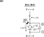
図6は、発光動作(画像の表示)を行う回路の状態の例を示す図である。 FIG. 6 is a diagram illustrating an example of a state of a circuit that performs a light emission operation (image display).
図6に示すように、スイッチ11を導通状態とし、正方向のバイアスを印加した場合、EL素子12に順方向の発光電流I_el1が流れ、素子が発光する。このとき、寄生容量13には、EL素子12のアノード電極側に正電荷が、カソード電極側に負電荷が、それぞれ発光電流I_el1の量に応じた量だけ蓄積される。例えば、発光電流I_el1の量が多く、発光のレベルが高い程(輝度が高い程)、EL素子12の両電極間にかかる電位差が大きくなり、寄生容量13に蓄積される電荷の量も多くなる。
As shown in FIG. 6, when the
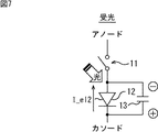
図7は、受光動作を行う回路の状態の例を示す図である。 FIG. 7 is a diagram illustrating an example of a state of a circuit that performs a light receiving operation.
図7に示すように、0V近傍のバイアスを印可した状態(スイッチ11を非導通にした状態)で外部から光が照射された場合、発光電流I_el1と反対方向の受光電流I_el2が流れる。
As shown in FIG. 7, when light is irradiated from the outside with a bias in the vicinity of 0 V (the
このときEL素子12は発光しない。また、発光電流I_el1と受光電流I_el2は向きが逆であるため、発光動作のときと反対の極性の電荷が寄生容量13に蓄積される。
At this time, the
この状態は所定の期間保持される。従って、その所定の期間にEL素子12により発生された電荷が全て寄生容量13に蓄積される。
This state is maintained for a predetermined period. Therefore, all the charges generated by the
所定の期間の経過後、寄生容量13に蓄積された全体の電荷の量に基づいて外部からの入力が検出される。すなわち、寄生容量13に接続されるパス(図示せず)から、蓄積された電荷全体が取り出され、入力が検出される。
After the elapse of a predetermined period, an external input is detected based on the total amount of charges accumulated in the
このように、所定の期間に発生された電荷全体に基づいて外部からの入力を検出するようにしたため、発生された電荷を順次取り出して外部からの入力を検出する場合に較べて、電荷の量を表す信号(電流値を表す信号、電流値を電圧値に変換して得られる電圧値を表す信号)の振幅を大きくとることができ、それに基づいて行う入力の検出が容易になる。 As described above, since the input from the outside is detected based on the entire charge generated in a predetermined period, the amount of charge is larger than that in the case where the generated charges are sequentially taken out and the input from the outside is detected. (A signal representing a current value, a signal representing a voltage value obtained by converting a current value into a voltage value) can be increased in amplitude, and input detection performed based on the amplitude can be facilitated.
次に、図8乃至図12を参照して、発光から受光までの一連の動作を、より具体的な回路の例を用いて説明する。 Next, a series of operations from light emission to light reception will be described with reference to FIGS. 8 to 12 using more specific circuit examples.
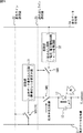
図8は、I/Oディスプレイ1を構成する各画素内の回路の例を示す図である。図6等に対応する構成には同一の符号を付してある。
FIG. 8 is a diagram illustrating an example of a circuit in each pixel constituting the I /
スイッチSW1乃至SW3は、アモルファスシリコンやポリシリコンなどで形成されるスイッチング素子である。 The switches SW1 to SW3 are switching elements formed of amorphous silicon or polysilicon.
このうちのスイッチSW1(例えば、図6のスイッチ11に対応する)は、表示ライン選択線22によりその導通/非導通が制御され、導通状態のとき、表示データ信号線21から供給される、表示データを表す信号を回路群31に出力する。表示データを表す信号は、例えば、制御装置2から供給されてくるものである。
Among these switches, the switch SW1 (for example, corresponding to the
スイッチSW2は、制御装置2によるEL素子発光制御に従って、その導通/非導通が制御され、導通状態のとき、回路群31の出力をEL素子12に供給する。
The switch SW2 controls conduction / non-conduction in accordance with the EL element light emission control by the
スイッチSW3は、読み出しライン選択線23によりその導通/非導通が制御され、導通状態のとき、EL素子12が所定の期間光の照射を受けることにより発生したリーク電流(寄生容量13に蓄積された電荷)を回路群32に供給する。すなわち、スイッチSW3は、受光動作が開始されてから所定の期間経過後に導通状態にされるスイッチである。
The switch SW3 has its conduction / non-conduction controlled by the readout
回路群31は、例えば、表示データ書き込み回路、閾値ばらつき補正回路などからなる。表示データ書き込み回路は、スイッチSW1から供給されてきた信号を一時的に蓄積し、EL素子12を発光させるためのI/V(電流/電圧)変換を行う回路である。閾値ばらつき補正回路は、例えば、スイッチSW1の出力に現れる信号のばらつきを補正する回路(TFTの閾値補正回路)である。
The circuit group 31 includes, for example, a display data writing circuit, a threshold value variation correcting circuit, and the like. The display data writing circuit is a circuit that temporarily accumulates the signal supplied from the switch SW1 and performs I / V (current / voltage) conversion for causing the
回路群32は、例えば、読み出し回路、電流・電圧増幅回路、A/D(Analog/Digital)変換回路などからなる。読み出し回路は、EL素子12で発生された受光信号をスイッチSW3を介して読み出す回路であり、電流・電圧増幅回路は、受光電流や、受光電流に対応する電圧を増幅させる回路である。A/D変換回路は、電流・電圧増幅回路により増幅された電流値、電圧値をディジタルデータ(受光データ)に変換し、受光データ信号線24に出力する。受光データ信号線24に出力された受光データは制御装置2に供給され、制御装置2により外部からの光の入力が検出される。
The
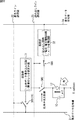
図8においては、スイッチSW1乃至SW3がいずれも非導通の状態である。この状態は、発光動作、受光動作のいずれの動作も行われていない状態である。 In FIG. 8, the switches SW1 to SW3 are all in a non-conductive state. This state is a state in which neither light emission operation nor light reception operation is performed.
このような状態の画素に発光動作を行わせる場合、始めに、図9に示すように、表示ライン選択線22によりスイッチSW1が導通状態にされる。このとき、表示データ信号線21から供給されてきた表示データを表す信号がスイッチSW1を介して回路群31に入力される。回路群31においてはI/V変換やばらつきの補正が行われる。
When the pixel in such a state is caused to perform a light emitting operation, first, as shown in FIG. 9, the switch SW <b> 1 is turned on by the display
次に、図10に示すように、スイッチSW1が非導通状態にされた後に、制御装置2によりEL素子発光制御が行われ、スイッチSW2が導通状態にされることに応じて、表示データに相当する発光電流I_el1が回路群31からEL素子12に流れる。これにより、表示データに応じたレベルでEL素子12が発光する。
Next, as shown in FIG. 10, after the switch SW1 is turned off, the EL light emission control is performed by the
このとき、EL素子12のアノード−カソード電極間には、発光のレベルに相当する電位差、すなわち表示データに相当する電位差がかかっており、電位差に応じた電荷が寄生容量13に蓄積される。この図10の状態が、図6の状態に相当する。
At this time, a potential difference corresponding to the light emission level, that is, a potential difference corresponding to display data is applied between the anode and the cathode electrode of the
次に、発光動作を受光動作に切り替える場合、図11に示すように、スイッチSW2が非導通状態にされ、この状態が所定の期間保持される。外部からの光を受けることに応じてEL素子12により発生された電荷(受光信号I_el2)は寄生容量13に蓄積される。図11の例においては、EL素子12のカソード電極側のインピーダンスがアノード電極側と較べて低いため、寄生容量13のカソード電極側の電荷は抜けることになるが、アノード電極側には電荷を放電するパスが無いため負電荷が蓄積され続ける。この図11の状態が、図7の状態に相当する。
Next, when switching the light emitting operation to the light receiving operation, as shown in FIG. 11, the switch SW2 is turned off, and this state is maintained for a predetermined period. The charge (light reception signal I_el2) generated by the
図11の状態が所定の期間保持された後、図12に示すように、読み出しライン選択線23によりスイッチSW3が導通状態にされ、寄生容量13に蓄積された量の電荷に対応する電流がスイッチSW3を介して回路群32に供給される。また、スイッチSW3が導通状態にされている間にEL素子12により発生された受光信号I_el2も回路群32に供給される。
After the state of FIG. 11 is maintained for a predetermined period, as shown in FIG. 12, the switch SW3 is turned on by the read
回路群32においては、供給されてきた信号に対して増幅等の所定の処理が施され、得られた受光データが受光データ信号線24を介して制御装置2に出力される。
In the
以上の動作により、寄生容量13に蓄積された全体の電荷の量に基づいて、外部からの入力の検出が行われることになる。このように各画素の動作を制御する制御装置2の処理についてはフローチャートを参照して後述する。
With the above operation, input from the outside is detected based on the total amount of charges accumulated in the
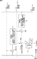
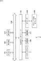
図13は、制御装置2の構成例を示すブロック図である。
FIG. 13 is a block diagram illustrating a configuration example of the
CPU(Central Processing Unit)101は、ROM(Read Only Memory)102に記憶されているプログラム、または、記憶部106からRAM(Random Access Memory)103にロードされたプログラムに従って各種の処理を実行する。RAM103にはまた、CPU101が各種の処理を実行する上において必要なデータなどが適宜記憶される。
A CPU (Central Processing Unit) 101 executes various processes according to a program stored in a ROM (Read Only Memory) 102 or a program loaded from a
CPU101、ROM102、およびRAM103は、バス104を介して相互に接続されている。このバス104にはまた、入出力インタフェース105も接続されている。
The
入出力インタフェース105には、I/Oディスプレイ1の他、ハードディスクなどより構成される記憶部106、ネットワークを介しての通信処理を行う通信部107などが接続される。
In addition to the I /
入出力インタフェース105にはまた、必要に応じてドライブ108が接続され、磁気ディスク、光ディスク、光磁気ディスク、或いは半導体メモリなどよりなるリムーバブルメディア109が適宜装着され、それから読み出されたコンピュータプログラムが、必要に応じて記憶部106にインストールされる。
A
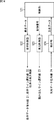
図14は、制御装置2の機能構成例を示すブロック図である。
FIG. 14 is a block diagram illustrating a functional configuration example of the
図14に示す構成の少なくとも一部は、図13のCPU101により所定のプログラムが実行されることで実現される。
At least a part of the configuration shown in FIG. 14 is realized by executing a predetermined program by the
制御部121は、例えば、取得した表示データを表示制御部122に出力し、発光動作を行うI/Oディスプレイ1の画素を用いて表示データを表示させる(表示データに対応するレベルで発光させる)。
For example, the
また、制御部121は、受光制御部123を制御して、I/Oディスプレイ1の所定の画素に受光動作を行わせる。制御部121は、検出部124から受光データが供給されてきたとき、それに基づいて所定の処理を行う。
The
表示制御部122は、制御部121から供給されてきた表示データに基づいて、発光動作を行わせる画素のラインを表示ライン選択線22により選択し、表示データを表す信号を表示データ信号線21から供給させることによって、選択したラインの画素に発光動作を行わせる。また、表示制御部122は、所定のタイミングでEL素子発光制御を行い、スイッチSW2を導通状態にさせる。
Based on the display data supplied from the
受光制御部123は、制御部121による制御に従って、受光動作を行わせる画素のラインを読み出しライン選択線23により選択し、受光動作が開始されてから所定の期間検出後、スイッチSW3を導通状態にする。
Under the control of the
検出部124は、受光データ信号線24を介して供給されてくる受光データに基づいて、光を介して外部から入力されたデータを検出し、検出した受光データを制御部121に出力する。
The
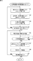
次に、図15のフローチャートを参照して、以上のような構成を有する制御装置2により行われるI/Oディスプレイ1の制御処理について説明する。例えば、図8に示すような状態で、制御部121から表示制御部122に表示データが供給されたときにこの処理が開始される。
Next, with reference to the flowchart of FIG. 15, the control process of the I /
ステップS1において、表示制御部122は、制御部121から供給されてきた表示データに基づいて、発光動作を行わせる画素のラインを表示ライン選択線22により選択し、選択したラインの画素のスイッチSW1を導通状態(ON)にさせる(図9)。
In step S <b> 1, the
また、表示制御部122は、ステップS2において、発光動作を行わせる画素に対して、表示データを表す信号を表示データ信号線21から供給し、ステップS3に進み、EL素子発光制御を行う。これによりスイッチSW2が導通状態になり、回路群31において所定の処理が施されることによって得られた発光電流I_el1がEL素子12に流れ、EL素子12が発光する(図10)。
In step S2, the
なお、表示制御部122によっては、EL素子発光制御の前にスイッチSW1を非導通状態(OFF)にすること、および、EL素子12を発光させた後にスイッチSW2を非導通状態にすることも行われる。
Depending on the
表示制御部122は、ステップS4において、発光動作を行わせた画素の動作を受光動作に切り替えるか否かを判定し、切り替えないと判定した場合、ステップS1に戻り、上述した処理を繰り返す。
In step S4, the
ステップS4において、発光動作を行わせた画素の動作を受光動作に切り替えると表示制御部122により判定された場合、処理はステップS5に進む。
In step S4, when the
ステップS5においては、スイッチSW2の非導通状態は保持され、光を受けることに応じてEL素子12により発生された電荷が寄生容量13に蓄積され続ける(図11)。
In step S5, the non-conducting state of the switch SW2 is maintained, and the charge generated by the
ステップS6において、受光制御部123は、受光動作を行わせている画素のスイッチSW2が非導通状態になってから所定の期間経過したか否かを判定し、経過したと判定するまで待機する。
In step S6, the light
受光制御部123は、ステップS6において、スイッチSW2が非導通状態になってから所定の期間経過したと判定した場合、ステップS7に進み、受光動作を行わせた画素のスイッチSW3を導通状態にすることで、EL素子12により発生され、寄生容量13に蓄積されていた電荷に対応する信号を回路群32に供給させる。
If the light
回路群32に供給された受光電流I_el2に対しては、増幅等の所定の処理が施され、得られた受光データが受光データ信号線24を介して制御装置2の検出部124に供給される(図12)。
The light reception current I_el2 supplied to the
ステップS8において、検出部124は、受光データ信号線24を介して供給されてきた受光データを検出し、検出した受光データを制御部121に出力する。
In step S <b> 8, the
ステップS9において、受光制御部123は、受光動作を終了させるか否かを判定し、終了させないと判定した場合、スイッチSW3を非導通状態にさせた後、ステップS5に戻り、それ以降の処理を行わせる。受光制御部123は、ステップS9において、終了させると判定したとき、処理を終了させる。
In step S9, the light
以上の処理をそれぞれの画素に繰り返し行わせることによって、画像の表示と光の検出を行わせることができる。また、その光の検出の際の受光感度を上げることが可能になる。 By repeating the above processing for each pixel, it is possible to display an image and detect light. In addition, it is possible to increase the light receiving sensitivity when detecting the light.
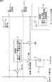
以上においては、EL素子12により発生された電荷を蓄積する素子として寄生容量13が用いられるとしたが、図16に示すように、EL素子12に寄生する容量ではない容量131を、EL素子12に並列に設けるようにしてもよい。
In the above description, the
これにより、EL素子12により発生された電荷を、寄生容量13に依存することなく任意の量だけ容量131に蓄積させることができる。
As a result, the electric charge generated by the
また、図17に示すように、EL素子12に対して容量131を並列に接続するかしないかを切り替えることができるように、EL素子12のアノード電極と容量131の間にスイッチSW4を挿入するようにしてもよい。
In addition, as shown in FIG. 17, a switch SW4 is inserted between the anode electrode of the
スイッチSW4は、EL素子12が受光動作を行っているときには導通状態にされ、発光動作を行っているとき(発光動作を開始するとき)には非導通状態にされる。EL素子12に並列に接続される容量131は、発光動作時には時定数を増加させる素子として働き、EL素子12に常時接続されている場合には発光の応答性を損う作用を及ぼすため、このように発光動作のときにEL素子12に対して切り離すことができるようにすることにより、発光時の応答性が損なわれることを防止することができる。
The switch SW4 is turned on when the
このように、EL素子12により発生された電荷を蓄積する容量である容量131は、それぞれの画素内に設けられるものに限らず、図18に示すように、画素の外に、読み出しライン選択線23に接続されるようにして設けられるようにしてもよい。図18の例においては、画素の内部にはスイッチSW1,SW2,SW3、EL素子12、寄生容量13、および回路群31が設けられるものとし、容量131は、その外側(ゲート線(表示ライン選択線22)とソース線(表示データ信号線21)で囲まれる範囲の外側)に設けられる。
As described above, the
図19は、EL素子12により発生された電荷を蓄積する容量である容量131が、ディスプレイの外側に設けられる例を示している。ここで、ディスプレイとは、スイッチSW1,SW2,SW3、EL素子12、寄生容量13、および回路群31が設けられる画素が複数配列して構成されるディスプレイ面をいい、図19の例においては、このディスプレイ面の外側に容量131と回路群32が設けられている。
FIG. 19 shows an example in which a
すなわち、EL素子12により発生された電荷を蓄積することができる位置であれば、図18、図19に示すように、画素の外部、ディスプレイの外部などの様々な位置に容量131を設けることが可能である。
In other words, as long as the charge generated by the
以上においては、図1に示したように、制御装置2はI/Oディスプレイ1に内蔵されるとしたが、当然、I/Oディスプレイ1の外部に設けられるようにしてもよい。
In the above description, as shown in FIG. 1, the
上述した一連の処理は、ハードウェアにより実行させることもできるが、ソフトウェアにより実行させることもできる。 The series of processes described above can be executed by hardware, but can also be executed by software.
一連の処理をソフトウェアにより実行させる場合には、そのソフトウェアを構成するプログラムが、専用のハードウェアに組み込まれているコンピュータ、または、各種のプログラムをインストールすることで、各種の機能を実行することが可能な、例えば、汎用のパーソナルコンピュータなどに、ネットワークや記録媒体からインストールされる。 When a series of processing is executed by software, a program constituting the software may execute various functions by installing a computer incorporated in dedicated hardware or various programs. For example, it is installed from a network or a recording medium into a general-purpose personal computer or the like.
この記録媒体は、図13に示されるように、装置本体とは別に、ユーザにプログラムを提供するために配布される、プログラムが記録されている磁気ディスク(フレキシブルディスクを含む)、光ディスク(CD-ROM(Compact Disk-Read Only Memory),DVD(Digital Versatile Disk)を含む)、光磁気ディスク(MD(登録商標)(Mini-Disk)を含む)、もしくは半導体メモリなどよりなるリムーバブルメディア109により構成されるだけでなく、装置本体に予め組み込まれた状態でユーザに提供される、プログラムが記録されているROM102や、記憶部106に含まれるハードディスクなどで構成される。
As shown in FIG. 13, the recording medium is distributed to provide a program to the user separately from the apparatus main body, and includes a magnetic disk (including a flexible disk) on which the program is recorded, an optical disk (CD- ROM (Compact Disk-Read Only Memory), DVD (including Digital Versatile Disk)), magneto-optical disk (including MD (registered trademark) (Mini-Disk)), or
なお、本明細書において、各ステップは、記載された順序に従って時系列的に行われる処理はもちろん、必ずしも時系列的に処理されなくとも、並列的あるいは個別に実行される処理をも含むものである。 In the present specification, each step includes not only processing performed in time series according to the described order but also processing executed in parallel or individually, although not necessarily performed in time series.
1 I/Oディスプレイ, 2 制御装置, 11 スイッチ, 12 EL素子, 13 寄生容量, 121 制御装置, 122 表示制御部, 123 受光制御部, 124 検出部 1 I / O display, 2 control device, 11 switch, 12 EL element, 13 parasitic capacitance, 121 control device, 122 display control unit, 123 light reception control unit, 124 detection unit
Claims (5)
前記EL素子と並列に設けられる容量と、 A capacitor provided in parallel with the EL element;
表示データを表す信号の伝送に用いられる表示データ信号線に接続されるとともに、発光動作を行わせる画素の選択に用いられる表示ライン選択線を介して導通/非導通が制御される第1のスイッチと、 A first switch that is connected to a display data signal line used for transmission of a signal representing display data and whose conduction / non-conduction is controlled via a display line selection line used for selection of a pixel that performs a light emitting operation. When,
前記EL素子のアノード電極と前記第1のスイッチの間に設けられる第2のスイッチと、 A second switch provided between the anode electrode of the EL element and the first switch;
前記EL素子のアノード電極に接続され、受光動作を行わせる画素の選択に用いられる読み出しライン選択線を介して導通/非導通が制御される第3のスイッチと、 A third switch connected to the anode electrode of the EL element, the conduction / non-conduction of which is controlled via a readout line selection line used for selection of a pixel for performing a light receiving operation;
前記EL素子のアノード電極と前記容量の間に設けられる第4のスイッチと、 A fourth switch provided between the anode electrode of the EL element and the capacitor;
前記第3のスイッチを介して供給された信号をデータに変換し、前記データの伝送に用いられる受光データ信号線に出力する変換回路と A conversion circuit for converting a signal supplied via the third switch into data and outputting the data to a light reception data signal line used for transmission of the data;
が各画素に配置されたディスプレイと、 A display arranged in each pixel;
前記ディスプレイの画素の前記第1乃至第4のスイッチが非導通の状態において、所定の画素に発光動作を行わせる場合、発光動作を行わせる画素を、前記表示ライン選択線を介して前記第1のスイッチを導通状態として前記表示データを表す信号を導通させ、前記第1のスイッチを非導通状態とした後、前記第2のスイッチを導通状態として、前記第2のスイッチを介して前記表示データを表す信号を前記EL素子に供給させて前記EL素子を発光させるように制御し、発光動作を行っていた画素に受光動作を行わせる場合、受光動作を行わせる画素を、前記第4のスイッチを導通状態、前記第2のスイッチを非導通状態とし、光が照射されることに応じて前記EL素子が発生した電荷を前記第4のスイッチを介して前記容量に蓄積させ、所定の期間経過後に、前記読み出しライン選択線を介して前記第3のスイッチを導通状態とし、前記容量に蓄積させた電荷を前記第4のスイッチと前記第3のスイッチを介して前記変換回路に供給させ、前記変換回路から前記データを出力させるように制御する制御手段と、 When the first to fourth switches of the display pixels are in a non-conducting state, when causing a predetermined pixel to perform a light emission operation, the pixel that performs the light emission operation is selected via the display line selection line. The switch is turned on to turn on a signal representing the display data, and the first switch is turned off. Then, the second switch is turned on and the display data is passed through the second switch. When the EL element is controlled so as to emit light and the pixel that has performed the light emitting operation performs the light receiving operation, the pixel that performs the light receiving operation is set to the fourth switch. And the second switch is turned off, and the charge generated by the EL element in response to light irradiation is accumulated in the capacitor via the fourth switch. After the elapse, the third switch is made conductive through the readout line selection line, and the charge accumulated in the capacitor is supplied to the conversion circuit through the fourth switch and the third switch, Control means for controlling the conversion circuit to output the data;
受光動作を行っていた画素から前記受光データ信号線を介して供給された前記データを検出する検出手段と Detecting means for detecting the data supplied from the pixel that has been performing the light receiving operation via the light receiving data signal line;
を備える表示装置。 A display device comprising:
請求項1に記載の表示装置。 The display device according to claim 1.
前記EL素子と並列に設けられる容量と、 A capacitor provided in parallel with the EL element;
表示データを表す信号の伝送に用いられる表示データ信号線に接続されるとともに、発光動作を行わせる画素の選択に用いられる表示ライン選択線を介して導通/非導通が制御される第1のスイッチと、 A first switch that is connected to a display data signal line used for transmission of a signal representing display data and whose conduction / non-conduction is controlled via a display line selection line used for selection of a pixel that performs a light emitting operation. When,
前記EL素子のアノード電極と前記第1のスイッチの間に設けられる第2のスイッチと、 A second switch provided between the anode electrode of the EL element and the first switch;
前記EL素子のアノード電極に接続され、受光動作を行わせる画素の選択に用いられる読み出しライン選択線を介して導通/非導通が制御される第3のスイッチと、 A third switch connected to the anode electrode of the EL element, the conduction / non-conduction of which is controlled via a readout line selection line used for selection of a pixel for performing a light receiving operation;
前記EL素子のアノード電極と前記容量の間に設けられる第4のスイッチと、 A fourth switch provided between the anode electrode of the EL element and the capacitor;
前記第3のスイッチを介して供給された信号をデータに変換し、前記データの伝送に用いられる受光データ信号線に出力する変換回路と A conversion circuit for converting a signal supplied via the third switch into data and outputting the data to a light reception data signal line used for transmission of the data;
が各画素に配置されたディスプレイを備える表示装置の制御方法において、 In a control method of a display device including a display arranged in each pixel,
前記ディスプレイの画素の前記第1乃至第4のスイッチが非導通の状態において、所定の画素に発光動作を行わせる場合、発光動作を行わせる画素を、前記表示ライン選択線を介して前記第1のスイッチを導通状態として前記表示データを表す信号を導通させ、前記第1のスイッチを非導通状態とした後、前記第2のスイッチを導通状態として、前記第2のスイッチを介して前記表示データを表す信号を前記EL素子に供給させて前記EL素子を発光させるように制御し、 When the first to fourth switches of the display pixels are in a non-conducting state, when causing a predetermined pixel to perform a light emission operation, the pixel that performs the light emission operation is selected via the display line selection line. The switch is turned on to turn on a signal representing the display data, and the first switch is turned off. Then, the second switch is turned on and the display data is passed through the second switch. To control the EL element to emit light by supplying a signal representing the EL element,
発光動作を行っていた画素に受光動作を行わせる場合、受光動作を行わせる画素を、前記第4のスイッチを導通状態、前記第2のスイッチを非導通状態とし、光が照射されることに応じて前記EL素子が発生した電荷を前記第4のスイッチを介して前記容量に蓄積させ、所定の期間経過後に、前記読み出しライン選択線を介して前記第3のスイッチを導通状態とし、前記容量に蓄積させた電荷を前記第4のスイッチと前記第3のスイッチを介して前記変換回路に供給させ、前記変換回路から前記データを出力させるように制御し、 When a light receiving operation is performed on a pixel that has performed a light emitting operation, the pixel that performs the light receiving operation is turned on with the fourth switch in a conductive state and the second switch in a nonconductive state. In response, the charge generated by the EL element is accumulated in the capacitor via the fourth switch, and after a predetermined period, the third switch is turned on via the read line selection line, and the capacitor The charge accumulated in the first switch is supplied to the conversion circuit via the fourth switch and the third switch, and the data is output from the conversion circuit.
受光動作を行っていた画素から前記受光データ信号線を介して供給された前記データを検出する Detecting the data supplied from the pixel that has been performing the light receiving operation via the light receiving data signal line
ステップを含む制御方法。 A control method including steps.
前記EL素子と並列に設けられる容量と、 A capacitor provided in parallel with the EL element;
表示データを表す信号の伝送に用いられる表示データ信号線に接続されるとともに、発光動作を行わせる画素の選択に用いられる表示ライン選択線を介して導通/非導通が制御される第1のスイッチと、 A first switch that is connected to a display data signal line used for transmission of a signal representing display data and whose conduction / non-conduction is controlled via a display line selection line used for selection of a pixel that performs a light emitting operation. When,
前記EL素子のアノード電極と前記第1のスイッチの間に設けられる第2のスイッチと、 A second switch provided between the anode electrode of the EL element and the first switch;
前記EL素子のアノード電極に接続され、受光動作を行わせる画素の選択に用いられる読み出しライン選択線を介して導通/非導通が制御される第3のスイッチと、 A third switch connected to the anode electrode of the EL element, the conduction / non-conduction of which is controlled via a readout line selection line used for selection of a pixel for performing a light receiving operation;
前記EL素子のアノード電極と前記容量の間に設けられる第4のスイッチと、 A fourth switch provided between the anode electrode of the EL element and the capacitor;
前記第3のスイッチを介して供給された信号をデータに変換し、前記データの伝送に用いられる受光データ信号線に出力する変換回路と A conversion circuit for converting a signal supplied via the third switch into data and outputting the data to a light reception data signal line used for transmission of the data;
が各画素に配置されたディスプレイを備える表示装置を制御するコンピュータに実行させるプログラムが記録された記録媒体において、 In a recording medium on which a program to be executed by a computer that controls a display device having a display arranged in each pixel is recorded,
前記ディスプレイの画素の前記第1乃至第4のスイッチが非導通の状態において、所定の画素に発光動作を行わせる場合、発光動作を行わせる画素を、前記表示ライン選択線を介して前記第1のスイッチを導通状態として前記表示データを表す信号を導通させ、前記第1のスイッチを非導通状態とした後、前記第2のスイッチを導通状態として、前記第2のスイッチを介して前記表示データを表す信号を前記EL素子に供給させて前記EL素子を発光させるように制御し、 When the first to fourth switches of the display pixels are in a non-conducting state, when causing a predetermined pixel to perform a light emission operation, the pixel that performs the light emission operation is selected via the display line selection line. The switch is turned on to turn on a signal representing the display data, and the first switch is turned off. Then, the second switch is turned on and the display data is passed through the second switch. To control the EL element to emit light by supplying a signal representing the EL element,
発光動作を行っていた画素に受光動作を行わせる場合、受光動作を行わせる画素を、前記第4のスイッチを導通状態、前記第2のスイッチを非導通状態とし、光が照射されることに応じて前記EL素子が発生した電荷を前記第4のスイッチを介して前記容量に蓄積させ、所定の期間経過後に、前記読み出しライン選択線を介して前記第3のスイッチを導通状態とし、前記容量に蓄積させた電荷を前記第4のスイッチと前記第3のスイッチを介して前記変換回路に供給させ、前記変換回路から前記データを出力させるように制御し、 When a light receiving operation is performed on a pixel that has performed a light emitting operation, the pixel that performs the light receiving operation is turned on with the fourth switch in a conductive state and the second switch in a nonconductive state. In response, the charge generated by the EL element is accumulated in the capacitor via the fourth switch, and after a predetermined period, the third switch is turned on via the read line selection line, and the capacitor The charge accumulated in the first switch is supplied to the conversion circuit via the fourth switch and the third switch, and the data is output from the conversion circuit.
受光動作を行っていた画素から前記受光データ信号線を介して供給された前記データを検出する Detecting the data supplied from the pixel that has been performing the light receiving operation via the light receiving data signal line
ステップを含む処理をコンピュータに実行させるプログラムが記録された記録媒体。 A recording medium on which a program for causing a computer to execute processing including steps is recorded.
前記EL素子と並列に設けられる容量と、 A capacitor provided in parallel with the EL element;
表示データを表す信号の伝送に用いられる表示データ信号線に接続されるとともに、発光動作を行わせる画素の選択に用いられる表示ライン選択線を介して導通/非導通が制御される第1のスイッチと、 A first switch that is connected to a display data signal line used for transmission of a signal representing display data and whose conduction / non-conduction is controlled via a display line selection line used for selection of a pixel that performs a light emitting operation. When,
前記EL素子のアノード電極と前記第1のスイッチの間に設けられる第2のスイッチと、 A second switch provided between the anode electrode of the EL element and the first switch;
前記EL素子のアノード電極に接続され、受光動作を行わせる画素の選択に用いられる読み出しライン選択線を介して導通/非導通が制御される第3のスイッチと、 A third switch connected to the anode electrode of the EL element, the conduction / non-conduction of which is controlled via a readout line selection line used for selection of a pixel for performing a light receiving operation;
前記EL素子のアノード電極と前記容量の間に設けられる第4のスイッチと、 A fourth switch provided between the anode electrode of the EL element and the capacitor;
前記第3のスイッチを介して供給された信号をデータに変換し、前記データの伝送に用いられる受光データ信号線に出力する変換回路と A conversion circuit for converting a signal supplied via the third switch into data and outputting the data to a light reception data signal line used for transmission of the data;
が各画素に配置されたディスプレイを備える表示装置を制御するコンピュータに実行させるプログラムにおいて、 In a program to be executed by a computer that controls a display device having a display arranged in each pixel,
前記ディスプレイの画素の前記第1乃至第4のスイッチが非導通の状態において、所定の画素に発光動作を行わせる場合、発光動作を行わせる画素を、前記表示ライン選択線を介して前記第1のスイッチを導通状態として前記表示データを表す信号を導通させ、前記第1のスイッチを非導通状態とした後、前記第2のスイッチを導通状態として、前記第2のスイッチを介して前記表示データを表す信号を前記EL素子に供給させて前記EL素子を発光させるように制御し、 When the first to fourth switches of the display pixels are in a non-conducting state, when causing a predetermined pixel to perform a light emission operation, the pixel that performs the light emission operation is selected via the display line selection line. The switch is turned on to turn on a signal representing the display data, and the first switch is turned off. Then, the second switch is turned on and the display data is passed through the second switch. To control the EL element to emit light by supplying a signal representing the EL element,
発光動作を行っていた画素に受光動作を行わせる場合、受光動作を行わせる画素を、前記第4のスイッチを導通状態、前記第2のスイッチを非導通状態とし、光が照射されることに応じて前記EL素子が発生した電荷を前記第4のスイッチを介して前記容量に蓄積させ、所定の期間経過後に、前記読み出しライン選択線を介して前記第3のスイッチを導通状態とし、前記容量に蓄積させた電荷を前記第4のスイッチと前記第3のスイッチを介して前記変換回路に供給させ、前記変換回路から前記データを出力させるように制御し、 When a light receiving operation is performed on a pixel that has performed a light emitting operation, the pixel that performs the light receiving operation is turned on with the fourth switch in a conductive state and the second switch in a nonconductive state. In response, the charge generated by the EL element is accumulated in the capacitor via the fourth switch, and after a predetermined period, the third switch is turned on via the read line selection line, and the capacitor The charge accumulated in the first switch is supplied to the conversion circuit via the fourth switch and the third switch, and the data is output from the conversion circuit.
受光動作を行っていた画素から前記受光データ信号線を介して供給された前記データを検出する Detecting the data supplied from the pixel that has been performing the light receiving operation via the light receiving data signal line
ステップを含む処理をコンピュータに実行させるプログラム。 A program that causes a computer to execute processing including steps.
Priority Applications (2)
| Application Number | Priority Date | Filing Date | Title |
|---|---|---|---|
| JP2004212986A JP4635498B2 (en) | 2004-07-21 | 2004-07-21 | Display device, control method, recording medium, and program |
| US11/182,409 US20060017717A1 (en) | 2004-07-21 | 2005-07-15 | Controlling apparatus and method, recording medium, program, and inputting/outputting apparatus |
Applications Claiming Priority (1)
| Application Number | Priority Date | Filing Date | Title |
|---|---|---|---|
| JP2004212986A JP4635498B2 (en) | 2004-07-21 | 2004-07-21 | Display device, control method, recording medium, and program |
Publications (2)
| Publication Number | Publication Date |
|---|---|
| JP2006030855A JP2006030855A (en) | 2006-02-02 |
| JP4635498B2 true JP4635498B2 (en) | 2011-02-23 |
Family
ID=35656642
Family Applications (1)
| Application Number | Title | Priority Date | Filing Date |
|---|---|---|---|
| JP2004212986A Expired - Fee Related JP4635498B2 (en) | 2004-07-21 | 2004-07-21 | Display device, control method, recording medium, and program |
Country Status (2)
| Country | Link |
|---|---|
| US (1) | US20060017717A1 (en) |
| JP (1) | JP4635498B2 (en) |
Families Citing this family (5)
| Publication number | Priority date | Publication date | Assignee | Title |
|---|---|---|---|---|
| JP4934976B2 (en) * | 2005-03-24 | 2012-05-23 | ソニー株式会社 | Display device and driving method of display device |
| JP4341661B2 (en) | 2005-11-22 | 2009-10-07 | ソニー株式会社 | Input device, input method, and input device manufacturing method |
| JP4838090B2 (en) * | 2006-10-13 | 2011-12-14 | グローバル・オーエルイーディー・テクノロジー・リミテッド・ライアビリティ・カンパニー | Panel current measuring method and panel current measuring device |
| KR100879059B1 (en) * | 2006-11-14 | 2009-01-15 | 기아자동차주식회사 | Cut valve |
| US12342429B2 (en) * | 2020-07-29 | 2025-06-24 | Sharp Kabushiki Kaisha | Light-emitting device and driving method for light-emitting device |
Family Cites Families (5)
| Publication number | Priority date | Publication date | Assignee | Title |
|---|---|---|---|---|
| US5382975A (en) * | 1991-08-30 | 1995-01-17 | Fuji Xerox Co., Ltd. | Image reading apparatus |
| JPH1069238A (en) * | 1996-08-26 | 1998-03-10 | Pioneer Electron Corp | Organic electrolumiescence display device |
| JPH11274444A (en) * | 1998-03-19 | 1999-10-08 | Toshiba Corp | X-ray imaging device |
| JP2001203078A (en) * | 2000-01-19 | 2001-07-27 | Tdk Corp | Driving device of light emitting and receiving element, light emitting and receiving device, communication system and display device |
| JP4200435B2 (en) * | 2002-09-10 | 2008-12-24 | ソニー株式会社 | Information processing apparatus and method, recording medium, and program |
-
2004
- 2004-07-21 JP JP2004212986A patent/JP4635498B2/en not_active Expired - Fee Related
-
2005
- 2005-07-15 US US11/182,409 patent/US20060017717A1/en not_active Abandoned
Also Published As
| Publication number | Publication date |
|---|---|
| JP2006030855A (en) | 2006-02-02 |
| US20060017717A1 (en) | 2006-01-26 |
Similar Documents
| Publication | Publication Date | Title |
|---|---|---|
| US11651736B2 (en) | Electronic display with hybrid in-pixel and external compensation | |
| JP4734529B2 (en) | Display device | |
| CN101251978B (en) | Display device and driving method thereof | |
| US11164520B2 (en) | Power off method of display device, and display device | |
| KR101451584B1 (en) | Organic light emitting diode display | |
| US10089932B2 (en) | Method for powering off display apparatus, and display apparatus | |
| JP4571375B2 (en) | Active drive type light emitting display device and drive control method thereof | |
| KR20080084730A (en) | Pixel circuits and display devices and their driving methods | |
| KR20080061268A (en) | Pixel circuit, display device, and driving method of pixel circuit | |
| CN109754754B (en) | Drive control circuit for driving pixel drive circuit and display device | |
| US20140055042A1 (en) | Controlling apparatus and method, recording medium, program and inputting and outputting apparatus | |
| US10726771B2 (en) | Pixel circuit, driving method and display device | |
| KR20090055476A (en) | Display | |
| JP2016109911A (en) | Display device, display method and program | |
| US20030117082A1 (en) | Organic electroluminescent device compensated pixel driver circuit | |
| JP4635498B2 (en) | Display device, control method, recording medium, and program | |
| JP6311170B2 (en) | Display device power-off method and display device | |
| JP5257075B2 (en) | Image display device | |
| JP5305242B2 (en) | Pixel drive circuit, light emitting device, drive control method thereof, and electronic apparatus | |
| JP2009069373A (en) | Image display device | |
| JP5015428B2 (en) | Display device | |
| JP2008180836A (en) | Display device having partial display function | |
| JP4665423B2 (en) | Display device and driving method thereof | |
| JP2006072227A (en) | Drive circuit of display device | |
| JP2010049075A (en) | Pixel circuit and display device |
Legal Events
| Date | Code | Title | Description |
|---|---|---|---|
| A621 | Written request for application examination |
Free format text: JAPANESE INTERMEDIATE CODE: A621 Effective date: 20070607 |
|
| A977 | Report on retrieval |
Free format text: JAPANESE INTERMEDIATE CODE: A971007 Effective date: 20100722 |
|
| A131 | Notification of reasons for refusal |
Free format text: JAPANESE INTERMEDIATE CODE: A131 Effective date: 20100727 |
|
| A521 | Request for written amendment filed |
Free format text: JAPANESE INTERMEDIATE CODE: A523 Effective date: 20100916 |
|
| TRDD | Decision of grant or rejection written | ||
| A01 | Written decision to grant a patent or to grant a registration (utility model) |
Free format text: JAPANESE INTERMEDIATE CODE: A01 Effective date: 20101026 |
|
| A01 | Written decision to grant a patent or to grant a registration (utility model) |
Free format text: JAPANESE INTERMEDIATE CODE: A01 |
|
| A61 | First payment of annual fees (during grant procedure) |
Free format text: JAPANESE INTERMEDIATE CODE: A61 Effective date: 20101108 |
|
| FPAY | Renewal fee payment (event date is renewal date of database) |
Free format text: PAYMENT UNTIL: 20131203 Year of fee payment: 3 |
|
| FPAY | Renewal fee payment (event date is renewal date of database) |
Free format text: PAYMENT UNTIL: 20131203 Year of fee payment: 3 |
|
| LAPS | Cancellation because of no payment of annual fees |