JP4200435B2 - Information processing apparatus and method, recording medium, and program - Google Patents
Information processing apparatus and method, recording medium, and program Download PDFInfo
- Publication number
- JP4200435B2 JP4200435B2 JP2003281480A JP2003281480A JP4200435B2 JP 4200435 B2 JP4200435 B2 JP 4200435B2 JP 2003281480 A JP2003281480 A JP 2003281480A JP 2003281480 A JP2003281480 A JP 2003281480A JP 4200435 B2 JP4200435 B2 JP 4200435B2
- Authority
- JP
- Japan
- Prior art keywords
- information processing
- display
- light
- data
- image
- Prior art date
- Legal status (The legal status is an assumption and is not a legal conclusion. Google has not performed a legal analysis and makes no representation as to the accuracy of the status listed.)
- Expired - Fee Related
Links
Images


Classifications
-
- G—PHYSICS
- G06—COMPUTING; CALCULATING OR COUNTING
- G06F—ELECTRIC DIGITAL DATA PROCESSING
- G06F3/00—Input arrangements for transferring data to be processed into a form capable of being handled by the computer; Output arrangements for transferring data from processing unit to output unit, e.g. interface arrangements
- G06F3/01—Input arrangements or combined input and output arrangements for interaction between user and computer
- G06F3/03—Arrangements for converting the position or the displacement of a member into a coded form
- G06F3/041—Digitisers, e.g. for touch screens or touch pads, characterised by the transducing means
- G06F3/0412—Digitisers structurally integrated in a display
-
- G—PHYSICS
- G06—COMPUTING; CALCULATING OR COUNTING
- G06F—ELECTRIC DIGITAL DATA PROCESSING
- G06F1/00—Details not covered by groups G06F3/00 - G06F13/00 and G06F21/00
- G06F1/16—Constructional details or arrangements
- G06F1/1613—Constructional details or arrangements for portable computers
-
- G—PHYSICS
- G06—COMPUTING; CALCULATING OR COUNTING
- G06F—ELECTRIC DIGITAL DATA PROCESSING
- G06F1/00—Details not covered by groups G06F3/00 - G06F13/00 and G06F21/00
- G06F1/16—Constructional details or arrangements
- G06F1/1613—Constructional details or arrangements for portable computers
- G06F1/1633—Constructional details or arrangements of portable computers not specific to the type of enclosures covered by groups G06F1/1615 - G06F1/1626
- G06F1/1684—Constructional details or arrangements related to integrated I/O peripherals not covered by groups G06F1/1635 - G06F1/1675
- G06F1/1698—Constructional details or arrangements related to integrated I/O peripherals not covered by groups G06F1/1635 - G06F1/1675 the I/O peripheral being a sending/receiving arrangement to establish a cordless communication link, e.g. radio or infrared link, integrated cellular phone
-
- G—PHYSICS
- G06—COMPUTING; CALCULATING OR COUNTING
- G06F—ELECTRIC DIGITAL DATA PROCESSING
- G06F3/00—Input arrangements for transferring data to be processed into a form capable of being handled by the computer; Output arrangements for transferring data from processing unit to output unit, e.g. interface arrangements
- G06F3/002—Specific input/output arrangements not covered by G06F3/01 - G06F3/16
-
- G—PHYSICS
- G06—COMPUTING; CALCULATING OR COUNTING
- G06F—ELECTRIC DIGITAL DATA PROCESSING
- G06F3/00—Input arrangements for transferring data to be processed into a form capable of being handled by the computer; Output arrangements for transferring data from processing unit to output unit, e.g. interface arrangements
- G06F3/01—Input arrangements or combined input and output arrangements for interaction between user and computer
- G06F3/02—Input arrangements using manually operated switches, e.g. using keyboards or dials
- G06F3/0227—Cooperation and interconnection of the input arrangement with other functional units of a computer
-
- G—PHYSICS
- G06—COMPUTING; CALCULATING OR COUNTING
- G06F—ELECTRIC DIGITAL DATA PROCESSING
- G06F3/00—Input arrangements for transferring data to be processed into a form capable of being handled by the computer; Output arrangements for transferring data from processing unit to output unit, e.g. interface arrangements
- G06F3/01—Input arrangements or combined input and output arrangements for interaction between user and computer
- G06F3/048—Interaction techniques based on graphical user interfaces [GUI]
- G06F3/0481—Interaction techniques based on graphical user interfaces [GUI] based on specific properties of the displayed interaction object or a metaphor-based environment, e.g. interaction with desktop elements like windows or icons, or assisted by a cursor's changing behaviour or appearance
-
- H—ELECTRICITY
- H04—ELECTRIC COMMUNICATION TECHNIQUE
- H04N—PICTORIAL COMMUNICATION, e.g. TELEVISION
- H04N25/00—Circuitry of solid-state image sensors [SSIS]; Control thereof
- H04N25/70—SSIS architectures; Circuits associated therewith
- H04N25/76—Addressed sensors, e.g. MOS or CMOS sensors
-
- G—PHYSICS
- G09—EDUCATION; CRYPTOGRAPHY; DISPLAY; ADVERTISING; SEALS
- G09G—ARRANGEMENTS OR CIRCUITS FOR CONTROL OF INDICATING DEVICES USING STATIC MEANS TO PRESENT VARIABLE INFORMATION
- G09G2300/00—Aspects of the constitution of display devices
- G09G2300/08—Active matrix structure, i.e. with use of active elements, inclusive of non-linear two terminal elements, in the pixels together with light emitting or modulating elements
- G09G2300/0809—Several active elements per pixel in active matrix panels
- G09G2300/0842—Several active elements per pixel in active matrix panels forming a memory circuit, e.g. a dynamic memory with one capacitor
Landscapes
- Engineering & Computer Science (AREA)
- Theoretical Computer Science (AREA)
- General Engineering & Computer Science (AREA)
- General Physics & Mathematics (AREA)
- Human Computer Interaction (AREA)
- Physics & Mathematics (AREA)
- Computer Hardware Design (AREA)
- Signal Processing (AREA)
- Multimedia (AREA)
- Control Of Indicators Other Than Cathode Ray Tubes (AREA)
- Controls And Circuits For Display Device (AREA)
- Liquid Crystal Display Device Control (AREA)
- Image Input (AREA)
- Position Input By Displaying (AREA)
- Control Of El Displays (AREA)
Description
本発明は、情報処理装置および方法、記録媒体、並びにプログラムに関し、特に、情報の送受信を、直感的に、かつ容易に行うことができるようにする情報処理装置および方法、記録媒体、並びにプログラムに関する。 The present invention relates to an information processing apparatus and method, a recording medium, and a program, and more particularly, to an information processing apparatus and method, a recording medium, and a program that enable intuitive transmission and reception of information. .
近年、タッチパネルなどを重畳して設けることなく、テレビジョン受像機などの表示装置に対して各種の情報を直接入力する技術が各種提案されている。 In recent years, various techniques for directly inputting various types of information to a display device such as a television receiver have been proposed without providing a touch panel or the like.
例えば、特許文献1には、表示装置(情報入出力装置)の内側から外側に向かって出射された赤外線の光量と、その反射光の光量に基づいて、ユーザの動作に対応する情報や、ユーザが提示したカードに表されている情報を検出させることが開示されている。これにより、ユーザは、マウスやキーボードを操作することなく、所定の情報を表示装置に入力することができる。
For example,
また、特許文献2には、表示装置を構成する素子である、光入力方式で書き込まれた情報に応じて発光表示が可能な有機EL素子について記載されている。
しかしながら、このように、ユーザの動作に対応する情報や、ユーザが提示したカードに表されている情報を検出させることで表示装置に情報を入力する場合、所定の時間内に入力できる情報の量に限界があるという課題があった。 However, when information is input to the display device by detecting information corresponding to the user's action or information displayed on the card presented by the user, the amount of information that can be input within a predetermined time There was a problem that there was a limit.
また、表示装置に情報を入力するためには、近年急激に普及しつつあるIEEE(Institute of Electrical and Electronics Engineers)802.11a,または802.11bなどのいわゆる無線LAN(Local Area Network)や、Bluetooth(登録商標)により通信を行うモジュールを表示装置に設け、同様の通信モジュールが設けられている情報端末から、無線通信により表示装置に情報を入力(送信)することも考えられるが、通信を開始するまでの設定が煩雑であり、情報を容易に入力することができないという課題がある。 In addition, in order to input information to a display device, so-called wireless LAN (Local Area Network) such as IEEE (Institute of Electrical and Electronics Engineers) 802.11a or 802.11b and Bluetooth (registered) It is conceivable to provide a display device with a module that performs communication according to a trademark, and input (transmit) information to the display device by wireless communication from an information terminal provided with a similar communication module. Is complicated, and there is a problem that information cannot be easily input.
さらに、ユーザは、情報端末の画面上でデータの送信を指示するため、例えば、タッチパネルが設けられている表示装置に対して情報を直接入力する場合(表示部を直接押下する場合)に較べて、情報を直感的に入力することができない。 Furthermore, since the user instructs data transmission on the screen of the information terminal, for example, compared with a case where information is directly input to a display device provided with a touch panel (when the display unit is directly pressed). Unable to input information intuitively.
本発明はこのような状況に鑑みてなされたものであり、表示装置との間における情報の送受信を、直感的に、かつ容易に行うことができるようにするものである。 The present invention has been made in view of such a situation, and makes it possible to intuitively and easily perform transmission and reception of information with a display device.
本発明の第1の情報処理装置は、他の情報処理装置に出力する出力データを表す複数の第1の図形画像を生成する生成手段と、生成手段により生成された複数の第1の図形画像のそれぞれを順次表示する表示手段と、所定の画像を表示する表示手段の表示領域の一部に、他の情報処理装置から入力されてくる入力データを表す第2の図形画像が検出される検出領域を形成する形成手段と、複数の第2の図形画像のそれぞれが、他の情報処理装置において順次表示されることに応じて、検出領域を構成する画素に配設されるトランジスタの活性半導体層において、外部からの光に応じて発生される電流に基づいて第2の図形画像を検出する検出手段と、検出手段により検出された複数の第2の図形画像に基づいて、入力データを取得する取得手段とを備える。 The first information processing apparatus according to the present invention includes a generation unit that generates a plurality of first graphic images representing output data to be output to another information processing apparatus, and a plurality of first graphic images generated by the generation unit. A second graphic image representing input data input from another information processing device is detected in a part of the display area of the display means for sequentially displaying each of the display means and the display means for displaying a predetermined image An active semiconductor layer of a transistor disposed in a pixel constituting the detection area in response to the formation means for forming the area and each of the plurality of second graphic images being sequentially displayed in another information processing apparatus , Input means is obtained based on a detection means for detecting a second graphic image based on a current generated in response to light from the outside and a plurality of second graphic images detected by the detection means. Acquisition hand Provided with a door.
本発明の第1の情報処理装置の情報処理方法は、他の情報処理装置に出力する出力データを表す複数の第1の図形画像を生成する生成ステップと、生成ステップの処理により生成された複数の第1の図形画像のそれぞれを順次表示する表示ステップと、所定の画像を表示する表示手段の表示領域の一部に、他の情報処理装置から入力されてくる入力データを表す第2の図形画像が検出される検出領域を形成する形成ステップと、複数の第2の図形画像のそれぞれが、他の情報処理装置において順次表示されることに応じて、検出領域を構成する画素に配設されるトランジスタの活性半導体層において、外部からの光に応じて発生される電流に基づいて第2の図形画像を検出する検出ステップと、検出ステップの処理により検出された複数の第2の図形画像に基づいて、入力データを取得する取得ステップとを含む。 An information processing method of a first information processing apparatus according to the present invention includes a generation step of generating a plurality of first graphic images representing output data to be output to another information processing apparatus, and a plurality of generations generated by processing of the generation step A display step for sequentially displaying each of the first graphic images, and a second graphic representing input data input from another information processing device in a part of the display area of the display means for displaying the predetermined image A forming step for forming a detection region in which an image is detected and each of the plurality of second graphic images are sequentially displayed on other information processing devices, and are arranged in pixels constituting the detection region. in the active semiconductor layer of that transistor, a detection step of detecting a second graphic image based on the current generated in response to light from the outside, a plurality of which are detected by the processing of the detection step the Based on the graphic image, including an acquisition step of acquiring input data.
本発明の第1の記録媒体に記録されているプログラムは、他の情報処理装置に出力する出力データを表す複数の第1の図形画像を生成する生成ステップと、生成ステップの処理により生成された複数の第1の図形画像のそれぞれを順次表示することを制御する表示制御ステップと、所定の画像を表示する表示手段の表示領域の一部に、他の情報処理装置から入力されてくる入力データを表す第2の図形画像が検出される検出領域を形成する形成ステップと、複数の第2の図形画像のそれぞれが、他の情報処理装置において順次表示されることに応じて、検出領域を構成する画素に配設されるトランジスタの活性半導体層において、外部からの光に応じて発生される電流に基づいて第2の図形画像を検出する検出制御ステップと、検出制御ステップの処理により検出された複数の第2の図形画像に基づいて、入力データを取得する取得ステップとを含む。 The program recorded on the first recording medium of the present invention is generated by a generation step for generating a plurality of first graphic images representing output data to be output to another information processing apparatus, and processing of the generation step Display control step for controlling the sequential display of each of the plurality of first graphic images, and input data input from another information processing apparatus to a part of the display area of the display means for displaying the predetermined image Forming a detection region in which a second graphic image representing the image is detected, and a plurality of second graphic images are sequentially displayed on another information processing apparatus to form the detection region in the active semiconductor layer of a transistor disposed in a pixel of a detection control step of detecting a second graphic image based on the current generated in response to light from the outside, the detection control stearate Based on the plurality of second graphic image detected by the processing of the flop, including an acquisition step of acquiring input data.
本発明の第1のプログラムは、他の情報処理装置に出力する出力データを表す複数の第1の図形画像を生成する生成ステップと、生成ステップの処理により生成された複数の第1の図形画像のそれぞれを順次表示することを制御する表示制御ステップと、所定の画像を表示する表示手段の表示領域の一部に、他の情報処理装置から入力されてくる入力データを表す第2の図形画像が検出される検出領域を形成する形成ステップと、複数の第2の図形画像のそれぞれが、他の情報処理装置において順次表示されることに応じて、検出領域を構成する画素に配設されるトランジスタの活性半導体層において、外部からの光に応じて発生される電流に基づいて第2の図形画像を検出する検出制御ステップと、検出制御ステップの処理により検出された複数の第2の図形画像に基づいて、入力データを取得する取得ステップとをコンピュータに実行させる。 The first program of the present invention includes a generation step for generating a plurality of first graphic images representing output data to be output to another information processing apparatus, and a plurality of first graphic images generated by the processing of the generation step And a second graphic image representing input data input from another information processing device in a part of the display area of the display means for displaying a predetermined image. A forming step for forming a detection area in which detection is performed, and each of the plurality of second graphic images is sequentially displayed on another information processing apparatus, and is arranged in a pixel constituting the detection area. in the active semiconductor layer of a transistor, a detection control step of detecting a second graphic image based on the current generated in response to light from the outside, is detected by the processing of the detection control step Based on the plurality of second graphic images, to execute an obtaining step of obtaining input data to the computer.
本発明の第2の情報処理装置は、他の情報処理装置に出力する出力データを表す複数の図形画像を生成する生成手段と、生成手段により生成された複数の図形画像のそれぞれを順次表示する表示手段と、音楽データに基づく音を出力する出力手段とを備え、表示手段は、出力データが音楽データである場合、出力手段による音の出力とともに、複数の図形画像のそれぞれを順次表示する。 The second information processing apparatus according to the present invention sequentially generates a plurality of graphic images representing output data to be output to another information processing apparatus, and a plurality of graphic images generated by the generation means. When the output data is music data, the display means sequentially displays each of the plurality of graphic images together with the output of the sound by the output means when the output data is music data.
前記図形画像は、その1つにより所定のデータ量のデータが表される2次元コードであるようにすることができる。 The graphic image may be a two-dimensional code in which a predetermined amount of data is represented by one of the graphic images.
1回の画面走査で1フレームの画像が表示される場合、前記表示手段は、1フレームの表示毎に複数の図形画像のそれぞれを表示するようにすることができる。 When one frame image is displayed by one screen scan, the display means can display each of a plurality of graphic images for each frame display.
前記表示手段は、出力データが画像データである場合、画像データに基づく画像を表示するとともに、その近傍に、図形画像を表示するようにすることができる。 When the output data is image data, the display means can display an image based on the image data and display a graphic image in the vicinity thereof.
本発明の第2の情報処理装置の情報処理方法は、他の情報処理装置に出力する出力データを表す複数の図形画像を生成する生成ステップと、生成ステップの処理により生成された複数の図形画像のそれぞれを順次表示する表示ステップとを含み、表示ステップの処理においては、出力データが音楽データである場合、音楽データに基づく音を出力する出力手段による音の出力とともに、複数の図形画像のそれぞれが順次表示される。 The information processing method of the second information processing apparatus of the present invention includes a generation step for generating a plurality of graphic images representing output data output to another information processing apparatus, and a plurality of graphic images generated by the processing of the generation step. sequential saw including a display step of displaying, respectively, in the processing of the display step, when the output data is music data, the output of sound by the output means for outputting a sound based on the music data, the plurality of graphic images Each is displayed sequentially.
本発明の第2の記録媒体に記録されているプログラムは、他の情報処理装置に出力する出力データを表す複数の図形画像を生成する生成ステップと、生成ステップの処理により生成された複数の図形画像のそれぞれを順次表示することを制御する表示制御ステップとを含み、表示制御ステップの処理においては、出力データが音楽データである場合、音楽データに基づく音を出力する出力手段による音の出力とともに、複数の図形画像のそれぞれが順次表示される。 The program recorded on the second recording medium of the present invention includes a generation step for generating a plurality of graphic images representing output data output to another information processing apparatus, and a plurality of graphics generated by the processing of the generation step. look including a display control step of controlling to sequentially display each image in the processing of the display control step, when the output data is music data, the sound by the output means for outputting a sound based on the music data output At the same time, each of the plurality of graphic images is sequentially displayed.
本発明の第2のプログラムは、他の情報処理装置に出力する出力データを表す複数の図形画像を生成する生成ステップと、生成ステップの処理により生成された複数の図形画像のそれぞれを順次表示することを制御する表示制御ステップとを含み、表示制御ステップの処理においては、出力データが音楽データである場合、音楽データに基づく音を出力する出力手段による音の出力とともに、複数の図形画像のそれぞれが順次表示される。 The second program of the present invention sequentially displays a generation step for generating a plurality of graphic images representing output data to be output to another information processing apparatus, and a plurality of graphic images generated by the processing of the generation step. look including a display control step of controlling that, in the context of processing of the display control step, when the output data is music data, the output of sound by the output means for outputting a sound based on the music data, the plurality of graphic images Each is displayed sequentially.
本発明の第3の情報処理装置は、所定の画像を表示する表示手段の表示領域の一部に、他の情報処理装置から入力されてくる入力データを表す図形画像が検出される検出領域を形成する形成手段と、複数の図形画像のそれぞれが、他の情報処理装置において順次表示されることに応じて、検出領域を構成する画素に配設されるトランジスタの活性半導体層において、外部からの光に応じて発生される電流に基づいて図形画像を検出する検出手段と、検出手段により検出された複数の図形画像に基づいて、入力データを取得する取得手段とを備える。 In the third information processing apparatus of the present invention, a detection area in which a graphic image representing input data input from another information processing apparatus is detected is part of a display area of a display unit that displays a predetermined image. The forming means for forming and each of the plurality of graphic images are sequentially displayed on the other information processing device, and in response to the external display in the active semiconductor layer of the transistor disposed in the pixel constituting the detection region, Detection means for detecting a graphic image based on a current generated according to light, and acquisition means for acquiring input data based on a plurality of graphic images detected by the detection means .
前記図形画像は、その1つにより所定のデータ量のデータが表される2次元コードであるようにすることができる。 The graphic image may be a two-dimensional code in which a predetermined amount of data is represented by one of the graphic images.
前記形成手段は、検出領域を構成させる表示領域の各画素に、画像を表示する各画素に対して印加される電圧と、逆方向の電圧を印加することで検出領域を形成するようにすることができる。 The forming means forms a detection region by applying a voltage in the opposite direction to a voltage applied to each pixel displaying an image to each pixel of the display region constituting the detection region. Can do.
前記形成手段は、表示手段による画面の走査に併せて順次移動されるように検出領域を形成するようにすることができる。 The forming unit may form the detection area so as to be sequentially moved along with the scanning of the screen by the display unit.
前記取得手段により、入力データに付随する、入力データの処理を指示する指示情報が取得されたとき、指示情報に基づいて入力データを処理する処理手段をさらに備えるようにすることができる。 When the acquisition unit acquires instruction information for instructing processing of input data accompanying the input data, the acquisition unit may further include a processing unit for processing the input data based on the instruction information.
前記取得手段により取得された入力データが画像データである場合、前記処理手段は、指示情報に基づいて、画像データに対応する画像の表示を制御するようにすることができる。 When the input data acquired by the acquisition unit is image data, the processing unit can control display of an image corresponding to the image data based on the instruction information.
前記処理手段は、指示情報に基づいて、前記取得手段により取得された入力データを保存するようにすることができる。 The processing means can store the input data acquired by the acquisition means based on the instruction information.
前記処理手段は、指示情報に基づいて、取得手段により取得された入力データの、他の機器への送信を制御するようにすることができる。 The processing means can control transmission of input data acquired by the acquiring means to another device based on the instruction information.
本発明の第3の情報処理装置の情報処理方法は、所定の画像を表示する表示手段の表示領域の一部に、他の情報処理装置から入力されてくる入力データを表す図形画像が検出される検出領域を形成する形成ステップと、複数の図形画像のそれぞれが、他の情報処理装置において順次表示されることに応じて、検出領域を構成する画素に配設されるトランジスタの活性半導体層において、外部からの光に応じて発生される電流に基づいて図形画像を検出する検出ステップと、検出ステップの処理により検出された複数の図形画像に基づいて、入力データを取得する取得ステップとを含む。 In the information processing method of the third information processing apparatus of the present invention, a graphic image representing input data input from another information processing apparatus is detected in a part of the display area of the display means for displaying a predetermined image. In the active semiconductor layer of the transistor disposed in the pixel constituting the detection region , each of the formation step for forming the detection region and each of the plurality of graphic images are sequentially displayed on another information processing device . includes a detection step of detecting a graphic image based on the current generated in response to light from the outside, based on the plurality of graphic images detected by the processing of the detection step, and an acquisition step of acquiring input data .
本発明の第3の記録媒体に記録されているプログラムは、所定の画像を表示する表示手段の表示領域の一部に、他の情報処理装置から入力されてくる入力データを表す図形画像が検出される検出領域を形成する形成ステップと、複数の図形画像のそれぞれが、他の情報処理装置において順次表示されることに応じて、検出領域を構成する画素に配設されるトランジスタの活性半導体層において、外部からの光に応じて発生される電流に基づいて図形画像を検出する検出制御ステップと、検出制御ステップの処理により検出された複数の図形画像に基づいて、入力データを取得する取得ステップとを含む。 The program recorded on the third recording medium of the present invention detects a graphic image representing input data input from another information processing apparatus in a part of the display area of the display means for displaying a predetermined image. Forming a detection region, and an active semiconductor layer of a transistor disposed in a pixel constituting the detection region in response to each of a plurality of graphic images being sequentially displayed in another information processing device Detection step for detecting a graphic image based on a current generated in response to light from the outside, and an acquisition step for acquiring input data based on a plurality of graphic images detected by the processing of the detection control step Including.
本発明の第3のプログラムは、所定の画像を表示する表示手段の表示領域の一部に、他の情報処理装置から入力されてくる入力データを表す図形画像が検出される検出領域を形成する形成ステップと、複数の図形画像のそれぞれが、他の情報処理装置において順次表示されることに応じて、検出領域を構成する画素に配設されるトランジスタの活性半導体層において、外部からの光に応じて発生される電流に基づいて図形画像を検出する検出制御ステップと、検出制御ステップの処理により検出された複数の図形画像に基づいて、入力データを取得する取得ステップとを含む。 The third program of the present invention forms a detection area in which a graphic image representing input data input from another information processing apparatus is detected in a part of the display area of the display means for displaying a predetermined image. In response to the formation step and each of the plurality of graphic images being sequentially displayed on another information processing device, the active semiconductor layer of the transistor disposed in the pixel constituting the detection region is exposed to light from the outside. A detection control step for detecting a graphic image based on a current generated in response thereto, and an acquisition step for acquiring input data based on a plurality of graphic images detected by the processing of the detection control step .
本発明の第4の情報処理装置は、電界発光素子に印加する電圧の方向を切り替えることで、電界発光素子による発光駆動と受光駆動を切り替える切替手段と、切替手段による切り替えによって受光駆動を行う電界発光素子が受光したときに発生する電流に基づいて、外部からの入力を検出する検出手段とを備え、切替手段が、所定の波長の光を出射する、発光駆動を行う素子である第1の電界発光素子を有する第1の画素の近傍に、所定の波長の光に対する受光感度が高い素子である、受光駆動を行う第2の電界発光素子を有する第2の画素を形成する場合、検出手段は、第2の電界発光素子が、第1の電界発光素子から出射された光の反射光を受光したときに発生する電流に基づいて、外部からの入力を検出する。 According to a fourth information processing apparatus of the present invention, by switching the direction of the voltage applied to the electroluminescent element, a switching unit that switches between light emission driving and light receiving drive by the electroluminescent element, and an electric field that performs light reception driving by switching by the switching unit. Detection means for detecting an input from the outside based on a current generated when the light emitting element receives light , and the switching means is a first element that emits light of a predetermined wavelength and performs light emission driving. In the case where a second pixel having a second electroluminescent element that performs light reception driving is formed in the vicinity of the first pixel having the electroluminescent element, which is an element having high light receiving sensitivity with respect to light of a predetermined wavelength. Detects the input from the outside based on the current generated when the second electroluminescent element receives the reflected light of the light emitted from the first electroluminescent element.
切替手段は、受光駆動を行う第2の電界発光素子を有する複数の第2の画素からなる検出領域を、表示部の所定の領域に形成するようにすることができる。 Switching means, a detection region comprising a plurality of second pixels having a second electroluminescent element for receiving the drive, it is possible to form in a predetermined area of the display unit.
切替手段は、検出領域と異なる表示部の領域に、発光駆動を行う第1の電界発光素子を有する複数の第1の画素からなる表示領域を形成するようにすることができる。 Switching means, in the area of different the detection area display unit, it is possible to form a display region comprising a plurality of first pixels having a first electroluminescent element for emitting light driving.
検出手段は、表示部の表面に所定の物体が近接されたことを外部からの入力として検出するようにすることができる。 The detecting means can detect that a predetermined object has approached the surface of the display unit as an input from the outside.
検出手段は、第2の電界発光素子が、第1の電界発光素子から出射された光の反射光を受光したときに発生する電流に基づいて、表示部の表面に接触、または、近接する物体の面情報を、外部からの入力として検出するようにすることができる。 The detecting means is an object that contacts or approaches the surface of the display unit based on a current generated when the second electroluminescent element receives reflected light of the light emitted from the first electroluminescent element. This surface information can be detected as an input from the outside.
表示部から離れた位置にある物体の像を結像する結像手段をさらに備え、検出手段は、受光駆動を行う第2の電界発光素子が受光したときに発生する電流に基づいて、結像手段により結像される物体の像を外部からの入力として検出するようにすることができる。 An image forming unit that forms an image of an object at a position away from the display unit is further provided, and the detection unit forms an image based on a current generated when the second electroluminescence element that performs light reception driving receives the light. The object image formed by the means can be detected as an input from the outside.
本発明の第4の情報処理方法は、電界発光素子に印加する電圧の方向を切り替えることで、電界発光素子による発光駆動と受光駆動を切り替える切替ステップと、切替ステップの処理による切り替えによって受光駆動を行う電界発光素子が受光したときに発生する電流に基づいて、外部からの入力を検出する検出ステップとを含み、切替ステップの処理により、所定の波長の光を出射する、発光駆動を行う素子である第1の電界発光素子を有する第1の画素の近傍に、所定の波長の光に対する受光感度が高い素子である、受光駆動を行う第2の電界発光素子を有する第2の画素が形成される場合、検出ステップの処理においては、第2の電界発光素子が、第1の電界発光素子から出射された光の反射光を受光したときに発生する電流に基づいて、外部からの入力が検出される。 According to a fourth information processing method of the present invention, the direction of the voltage applied to the electroluminescent element is switched to switch the light emission drive and the light reception drive by the electroluminescent element, and the light reception drive by the switching by the process of the switching step. electroluminescent device made based on the current occurs when the received, viewed including a detection step of detecting an input from the outside, by the process of switching step, emits light of a predetermined wavelength to emit light driving device In the vicinity of the first pixel having the first electroluminescent element, a second pixel having a second electroluminescent element that performs light reception driving, which is an element having high light receiving sensitivity to light of a predetermined wavelength, is formed. In the detection step, the second electroluminescent element is based on a current generated when the second electroluminescent element receives reflected light of the light emitted from the first electroluminescent element. Input from the outside is detected.
本発明の第4の記録媒体に記録されているプログラム、および、本発明の第4のプログラムは、電界発光素子に印加する電圧の方向を切り替えることで、電界発光素子による発光駆動と受光駆動を切り替える切替ステップと、切替ステップの処理による切り替えによって受光駆動を行う電界発光素子が受光したときに発生する電流に基づいて、外部からの入力を検出する検出ステップとを含み、切替ステップの処理により、所定の波長の光を出射する、発光駆動を行う素子である第1の電界発光素子を有する第1の画素の近傍に、所定の波長の光に対する受光感度が高い素子である、受光駆動を行う第2の電界発光素子を有する第2の画素が形成される場合、検出ステップの処理においては、第2の電界発光素子が、第1の電界発光素子から出射された光の反射光を受光したときに発生する電流に基づいて、外部からの入力が検出される。 The program recorded on the fourth recording medium of the present invention and the fourth program of the present invention perform light emission driving and light receiving driving by the electroluminescent element by switching the direction of the voltage applied to the electroluminescent element. a switching step of switching an electroluminescent element for receiving driving by switching by the processing switching step based on the current occurs when the received, viewed including a detection step of detecting an input from the outside, by the process of switching step In the vicinity of the first pixel that has the first electroluminescence element that emits light of a predetermined wavelength and performs light emission driving, the light reception driving that is an element having high light receiving sensitivity to light of the predetermined wavelength is performed. When the second pixel having the second electroluminescent element to be formed is formed, the second electroluminescent element is separated from the first electroluminescent element in the processing of the detection step. The reflected light Isa light based on the current generated when the received input from the outside is detected.
本発明の第1の情報処理装置および方法、並びにプログラムにおいては、他の情報処理装置に出力する出力データを表す複数の第1の図形画像が生成され、生成された複数の第1の図形画像のそれぞれが順次表示される。また、所定の画像を表示する表示手段の表示領域の一部に、他の情報処理装置から入力されてくる入力データを表す第2の図形画像が検出される検出領域が形成され、複数の第2の図形画像のそれぞれが、他の情報処理装置において順次表示されることに応じて、検出領域を構成する画素に配設されるトランジスタの活性半導体層において、外部からの光に応じて発生される電流に基づいて第2の図形画像が検出され、検出された複数の第2の図形画像に基づいて、入力データが取得される。 In the first information processing apparatus, method, and program of the present invention, a plurality of first graphic images representing output data to be output to another information processing apparatus are generated, and the generated first graphic images Each of these is displayed sequentially. In addition, a detection area in which a second graphic image representing input data input from another information processing apparatus is detected is formed in a part of the display area of the display unit for displaying a predetermined image, and a plurality of second areas are detected. Each of the two graphic images is generated in response to light from the outside in the active semiconductor layer of the transistor disposed in the pixel constituting the detection region in response to the sequential display on the other information processing apparatus. The second graphic image is detected based on the detected current, and the input data is acquired based on the plurality of detected second graphic images.
本発明の第2の情報処理装置および方法、並びにプログラムにおいては、他の情報処理装置に出力する出力データを表す複数の図形画像が生成され、生成された複数の図形画像のそれぞれが順次表示される。また、出力データが音楽データである場合、出力手段による音の出力とともに、複数の図形画像のそれぞれが順次表示される。 In the second information processing apparatus and method and program of the present invention, a plurality of graphic images representing output data to be output to another information processing apparatus are generated, and each of the generated plurality of graphic images is sequentially displayed. The When the output data is music data, each of the plurality of graphic images is sequentially displayed along with the sound output by the output means.
本発明の第3の情報処理装置および方法、並びにプログラムにおいては、所定の画像を表示する表示手段の表示領域の一部に、他の情報処理装置から入力されてくる入力データを表す図形画像が検出される検出領域が形成され、複数の図形画像のそれぞれが、他の情報処理装置において順次表示されることに応じて、検出領域を構成する画素に配設されるトランジスタの活性半導体層において、外部からの光に応じて発生される電流に基づいて図形画像が検出され、検出された複数の図形画像に基づいて、入力データが取得される。 In the third information processing apparatus, method, and program of the present invention, a graphic image representing input data input from another information processing apparatus is displayed in a part of the display area of the display means for displaying a predetermined image. In the active semiconductor layer of the transistor disposed in the pixels constituting the detection region , a detection region to be detected is formed, and each of the plurality of graphic images is sequentially displayed in another information processing device . A graphic image is detected based on a current generated in response to light from the outside , and input data is acquired based on the detected plurality of graphic images.
本発明の第4の情報処理装置および方法、並びにプログラムにおいては、電界発光素子に印加する電圧の方向を切り替えることで、電界発光素子による発光駆動と受光駆動が切り替えられ、受光駆動を行う電界発光素子が受光したときに発生する電流に基づいて、外部からの入力が検出される。また、所定の波長の光を出射する、発光駆動を行う素子である第1の電界発光素子を有する第1の画素の近傍に、所定の波長の光に対する受光感度が高い素子である、受光駆動を行う第2の電界発光素子を有する第2の画素を形成する場合、第2の電界発光素子が、第1の電界発光素子から出射された光の反射光を受光したときに発生する電流に基づいて、外部からの入力が検出される。 In the fourth information processing apparatus, method, and program of the present invention, the light emission drive and the light reception drive by the electroluminescence element are switched by switching the direction of the voltage applied to the electroluminescence element, and the light emission drive that performs the light reception drive. An external input is detected based on the current generated when the element receives light. In addition, a light receiving drive which is an element having a high light receiving sensitivity with respect to light of a predetermined wavelength in the vicinity of the first pixel having a first electroluminescent element which emits light of a predetermined wavelength and performs light emission driving. In the case of forming the second pixel having the second electroluminescent element that performs the above, the current generated when the second electroluminescent element receives the reflected light of the light emitted from the first electroluminescent element. Based on this, an external input is detected.
第1の本発明によれば、より直感的な操作で、かつ、容易に、外部の機器からデータを取り込むことができるとともに、その外部の機器に対して、容易に、データを転送することができる。 According to the first aspect of the present invention, data can be taken from an external device easily and more intuitively, and data can be easily transferred to the external device. it can.
第2の本発明によれば、より直感的な操作で、かつ、容易に、外部の機器に対してデータを転送することができる。 According to the second aspect of the present invention, data can be transferred to an external device easily and more intuitively.
第3の本発明によれば、より直感的な操作で、かつ、容易に、外部の機器からデータを取り込むことができる。 According to the third aspect of the present invention, data can be taken from an external device easily and more intuitively.
第4の本発明によれば、画像の表示とともに、外部からの入力を検出することができる。 According to the fourth aspect of the present invention, it is possible to detect external input as well as image display.
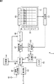
図1は、本発明を適用した情報処理システムの構成例を示す図である。 FIG. 1 is a diagram showing a configuration example of an information processing system to which the present invention is applied.
表示装置(情報処理装置)1の正面には、そのほぼ全体にわたって表示部11が形成されている。表示部11は、例えば、TFT(Thin Film Transistor)が各画素に配設された、有機または無機のEL(Electroluminescence)ディスプレイやLCD(Liquid Crystal Display)からなり、画素毎にその駆動を制御し、所定の図形や文字などの画像を表示する。
On the front surface of the display device (information processing device) 1, a
表示部11に表示されているウインドウ12には、動画像12Aが表示され、その右隅にマトリクス型の2次元コードであるシンボル13が表示されている。シンボル13は、動画像12Aのデータを表す図形画像であり、例えば、表示部11による1フレームの表示毎に、その白黒のパターンが切り換えられる。具体的には、表示装置1は、動画像12Aのソースデータを取得したとき、そのソースデータを表す、複数のシンボル(2次元コード)からなるシンボル列を生成し、1フレームの表示毎に各シンボルを順次表示する。
In the
従って、表示されるシンボルを検出し、それを解析することにより、シンボルを検出可能なリーダが設けられている機器は、表示部11に表示されるシンボルを介してソースデータを取得することができる。
Therefore, by detecting a displayed symbol and analyzing it, a device provided with a reader capable of detecting the symbol can acquire source data via the symbol displayed on the
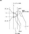
情報処理端末21は、PDA(Personal Digital Assistants)やパーソナルコンピュータ、或いは、携帯電話機などから構成され、ケーブル23を介して、表示装置1に表示されるシンボルを読み取り可能なリーダライタ24が接続されている。先端面24Aが表示部11に表示されているシンボル13に当接されたとき、リーダライタ24により、表示部11に表示されるシンボル13が読み取られる。
The
すなわち、リーダライタ24は、表示部11の表示周期に併せて、表示されるシンボル13のパターンを所定の期間だけ検出する。リーダライタ24により検出されたシンボルのデータは、ケーブル23を介して情報処理端末21に出力される。
That is, the reader /
情報処理端末21は、リーダライタ24から転送されたデータに基づいて、複数のシンボルが時系列的に並べられたシンボル列を取得し、さらに、取得したシンボル列からソースデータ(表示装置1により表示されている画像のソースデータ)を取得する。これにより、シンボル13を介して、表示装置1から情報処理端末21に対して、表示部11に表示されている画像に対応するデータが転送されることになる。
Based on the data transferred from the reader /
例えば、60Hzの周波数でプログレッシブ方式によりシンボルが順次表示され、かつ、1シンボルにより2KB(Byte)のデータが表される場合、960Kbps(60(回/秒)×2(KB)×8(bit))の転送レートでデータが転送されることになる。また、近年、400Hzの周波数で高画質な映像を表示できるディスプレイなども開発されているが、そのように非常に短い周期で、1つで2KBのデータが表されるシンボルが順次表示された場合、6400Kbps(400(回/秒)×2(KB)×8(bit))の転送レートでデータが転送されることになる。 For example, when symbols are sequentially displayed by a progressive method at a frequency of 60 Hz and 2 KB (Byte) data is represented by one symbol, 960 Kbps (60 (times / second) × 2 (KB) × 8 (bit) ) Data is transferred at a transfer rate. In recent years, displays that can display high-quality images at a frequency of 400 Hz have been developed, but when symbols that represent 2 KB of data are displayed one by one in such a very short cycle. Thus, data is transferred at a transfer rate of 6400 Kbps (400 (times / second) × 2 (KB) × 8 (bit)).
すなわち、IEEE(Institute of Electrical and Electronics Engineers)802.11a,802.11bなどのいわゆる無線LAN(Local Area Network)や、Bluetoothなどの無線通信によらずに、比較的高い転送レートでデータを送受信させることができる。 In other words, data can be transmitted and received at a relatively high transfer rate without using so-called wireless LAN (Local Area Network) such as IEEE (Institute of Electrical and Electronics Engineers) 802.11a, 802.11b, or wireless communication such as Bluetooth. it can.
なお、1つのシンボルにより表されるデータ量は、その大きさや誤り訂正の方式などにより適宜変更可能である。また、1つのシンボルにより表されるデータ量と、表示部11の表示周波数により、転送レートも適宜変更可能である。
Note that the amount of data represented by one symbol can be changed as appropriate depending on the size and error correction method. Further, the transfer rate can be appropriately changed according to the amount of data represented by one symbol and the display frequency of the
情報処理端末21においては、シンボル13を介して表示装置1から転送されたデータが内部の記憶部に保存されたり、或いは、転送されてきたデータに基づいて、対応する画像が表示部22に表示される。
In the
従って、ユーザは、リーダライタ24の先端面24Aを、表示されているシンボル13に当接させるといった、非常に直感的な操作により、表示装置1から情報処理端末21にデータを取り込ませることができる。
Therefore, the user can capture data from the
また、ユーザは、リーダライタ24の先端面24Aを、表示部11の所定の位置に形成された読み取り領域に当接させることで、上述したものと反対に、情報処理端末21から表示装置1に対してデータを入力することができる。
In addition, the user brings the
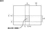
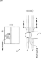
例えば、図2に示されるように、表示部11の右下に、表示装置1により読み取り領域31が形成され、そこに当接されたリーダライタ24から、シンボルを介してのデータの転送が行われる。
For example, as shown in FIG. 2, a
詳細な説明については後述するが、表示部11の各画素に配設されているTFTには、その画素により所定の画像の一部を表示させるとき、正方向のバイアス電圧が印加され、一方、その画素により、リーダライタ24において出力されるシンボルを検出させるとき、逆方向のバイアス電圧が印加される。従って、読み取り領域31は、例えば、表示部11の各画素のうち、逆方向のバイアス電圧が印加された複数の画素から構成される。
Although a detailed description will be given later, when a part of a predetermined image is displayed on the TFT disposed in each pixel of the
そのように逆方向のバイアス電圧が印加された画素(TFT)に対して、外部から光が入射されたとき(リーダライタ24からシンボルの白黒のパターンを表す光が入射されたとき)、TFTの活性半導体層ではリーク電流が発生するため、読み取り領域31を構成する各画素において検出されるリーク電流の有無に基づいて、各画素に対する、外部からの光の照射の有無が検出される。
When light is incident from the outside to the pixel (TFT) to which the reverse bias voltage is applied as described above (when light representing a black and white pattern of the symbol is incident from the reader / writer 24), Since a leak current is generated in the active semiconductor layer, the presence / absence of external light irradiation to each pixel is detected based on the presence / absence of the leak current detected in each pixel constituting the reading
すなわち、リーダライタ24の内部に設けられているシンボル表示部104(図8参照)にシンボルを表示させ、そのシンボルに対応する光が読み取り領域31に照射されたとき、読み取り領域31を構成する各画素において、光の有無、換言すれば、シンボルの白黒が検出される。
That is, when a symbol is displayed on the symbol display unit 104 (see FIG. 8) provided inside the reader /
具体的には、リーダライタ24内において表示されるシンボルのうち、黒色の部分が当接された読み取り領域31の画素ではリーク電流が発生されず、一方、白色の部分が当接された画素ではリーク電流が発生され、それが検出される。
Specifically, among the symbols displayed in the reader /
そして、読み取り領域31の各画素における検出結果が合成され、リーダライタ24内において表示された1つのシンボルが表示装置1により取得される。また、それが所定の期間繰り返されることで、リーダライタ24内において表示されたシンボル列(情報処理端末21から転送されてくるデータを表す全てのシンボル)が表示装置1に取り込まれる。表示装置1においては、情報処理端末21により表示装置1に転送するものとして選択されたデータがシンボル列の解析により復元され、取得される。
Then, the detection results in the respective pixels in the
これによりユーザは、表示部11に表示されるシンボル13にリーダライタ24を当接させるだけで表示装置1から情報処理端末21にデータを取り込むことができるとともに、リーダライタ24を読み取り領域31に当接させるだけで、情報処理端末21において選択したデータを表示装置1に転送することができる。
As a result, the user can capture data from the
すなわち、表示装置1と情報処理端末21との間で無線LANやBluetoothにより通信を行い、データを送受信する場合に較べて、煩雑な設定を行うことなく、直感的な操作で、容易にデータを送受信させることができる。
That is, compared with the case where communication is performed between the
なお、図2の例においては、表示部11に形成される読み取り領域31が点線で表されているが、ユーザが目視できるように、所定の大きさの枠画像が表示され、その枠の中に形成されるようにしてもよい。
In the example of FIG. 2, the
また、図2の例においては、表示部11のうち、読み取り領域31以外の領域にはいずれの画像も表示されていないが、逆方向のバイアス電圧が印加される読み取り領域31以外の領域には、テレビジョン番組の映像などの各種の画像を表示させておくことが可能である。
In the example of FIG. 2, no image is displayed in an area other than the reading
表示装置1と情報処理端末21との間で行われるデータの送受信については、フローチャートを参照して後に詳述する。
Data transmission / reception performed between the
図3は、図1の表示装置1の構成例を示すブロック図である。
FIG. 3 is a block diagram illustrating a configuration example of the
制御部45は、図示せぬROM(Read Only Memory)などに記憶されている制御プログラムに基づいて表示装置1の全体の動作を制御し、例えば、所定のチャンネルの番組の映像を表示させたり、所定のサイトにアクセスし、そのサイトの画面を表示させるなど、リモートコントローラなどよりなる入力部46からの、ユーザの指示に対応した処理を実行する。
The
信号処理部42は、制御部45による制御に基づいて、アンテナ41において受信されるテレビジョン放送波の中から所定のチャンネルの信号を取得し、そのチャンネルにより放送される番組のデータを制御部45に出力する。通信部43は、インターネットなどのネットワークを介して、各種の機器と有線または無線により通信し、取得したデータを制御部45に出力する。
Based on the control by the
記憶部44は、ハードディスクなどより構成され、情報処理端末21から転送されたデータ、テレビジョン番組の番組データ、通信部43により取得されたデータなど、各種のデータを記憶する。
The storage unit 44 includes a hard disk and stores various data such as data transferred from the
画像信号生成部47は、制御部45から供給されるデータに対応する画像を表示するための画像信号を生成し、生成した画像信号を、表示部11の駆動を制御するコントローラ48に出力する。
The image
また、画像信号生成部47は、シンボル処理部52により生成され、供給されたデータに基づいて、例えば、1画面毎(1フレームの表示毎)に1つのシンボルを表示させるための画像信号を生成し、それをコントローラ48に出力する。
Further, the image
コントローラ48は、表示部11の各画素に配設されるTFTのゲート電極に印加される電圧を制御するゲートドライバ50、および、ゲートドライバ50の駆動に連動して、TFTのソース電極−ドレイン電極間の電圧を制御するソースドライバ49の駆動を制御する。
The
例えば、コントローラ48は、表示部11の所定の位置に読み取り領域を形成することが制御部45から指示されたとき、読み取り領域を形成する画素(画素のTFT)には、逆方向のバイアス電圧が印加されるようにゲートドライバ50を制御するとともに、それ以外の領域には、正方向のバイアス電圧が印加されるようにゲートドライバ50を制御する。
For example, when the
これにより、読み取り領域を形成する画素は、ゲートがオフにされた状態となり、上述したように、外部から照射される光に対応したリーク電流の有無に基づいて、リーダライタ24において出力されているシンボルのパターンを検出することが可能となる。また、それ以外の画素は、ゲートがオンにされた状態となり、ソースドライバ49により供給される電圧に対応する電流により、画素電極に接続されているEL素子を発光し、画像の一部を表示する。
As a result, the pixels forming the reading region are in a state where the gate is turned off, and are output from the reader /
ここで、図4および図5を参照して、表示部11の各画素に配設されるTFTの動作についてより詳細に説明する。
Here, with reference to FIG. 4 and FIG. 5, the operation of the TFT arranged in each pixel of the
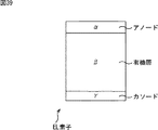
図4は、画像を表示する画素(シンボルの読み取り領域を構成する画素ではない画素)としてコントローラ48により制御された表示部11の1画素を示している。
FIG. 4 shows one pixel of the
例えば、ゲートドライバ50によりTFT71のゲート電極71A(G)に正方向の電圧が印加され、オンにされたとき、実線矢印で示されるように、ソースドライバ49により印加された電圧に応じて、アルファモスシリコンやポリシリコンからなる活性半導体層(チャネル)中を、ソース電極71B(S)からドレイン電極71C(D)方向に電流が流れる。
For example, when a positive voltage is applied to the
TFT71のドレイン電極71Cには、EL素子74のアノード電極74Aが接続されており、ドレイン電極71Cから供給された電流がEL素子74間を流れたとき、その電流に応じて、電界発光素子であるEL素子74が発光する。
The
このようにして発光された光が表示部11の表面を透過して表示装置1の外部に出射され、図4の画素により画像の一部が表示される。なお、図4においては、説明の便宜上、EL素子74から、白抜き矢印で示されるように図の右方向に光が出射されているが、実際には、アノード電極74Aまたはカソード電極74Bのいずれかが透明電極により構成され、その透明電極を透過して、EL素子74により発光された光が外部に出射される。
The light thus emitted passes through the surface of the
一方、ゲートドライバ50によりTFT71のゲート電極71A(G)に逆方向の電圧が印加され、ゲートがオフにされたとき、ソースドライバ49により電圧が印加された場合であっても活性半導体層中に電流が流れず、結果として、EL素子74に電流が流れないため発光が生じない。この状態において、図5の白抜き矢印で示されるように、外部から光が照射されたとき、TFT71の活性半導体層の光伝導性により、微量ではあるがドレイン電極71Cからソース電極71B方向にリーク電流(オフ電流)が発生する。また、EL素子74も、同様に、逆方向の電圧が印加された状態において光が照射されたとき、発光することなく、逆方向の電流を発生する。
On the other hand, when a reverse voltage is applied to the
このようにして発生した電流が検出され、図5の画素に外部から光が照射されたこと、すなわち、図5の画素に対応するリーダライタ24のシンボル表示部104(図8)の位置(図5の画素の正面)には、シンボルの白の領域が表示されていることが検出される。
The current generated in this way is detected, and the pixel of FIG. 5 is irradiated with light from the outside, that is, the position of the symbol display unit 104 (FIG. 8) of the reader /
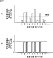
図6は、図4および図5に示される画素において発生された電流の計測結果を表している。図6において、横軸はゲート電極71Aに印加された電圧を表しており、縦軸は画素中の電流を表している。
FIG. 6 shows a measurement result of the current generated in the pixel shown in FIGS. In FIG. 6, the horizontal axis represents the voltage applied to the
計測結果l1は、正方向の電圧が印加された状態において、光が照射されたときにチャネル中を流れた電流の値を示しており、計測結果l2は、正方向の電圧が印加された状態において、光が照射されていないときにチャネル中を流れた電流の値を示している。 The measurement result l1 indicates the value of the current that flows through the channel when light is applied in a state where a positive voltage is applied, and the measurement result l2 indicates a state where a positive voltage is applied. Fig. 4 shows the value of the current that flows in the channel when no light is irradiated.
この計測結果l1およびl2により、正方向の電圧が印加されている場合は、外部からの光の有無に関わらず、ソースドライバ49により印加された電圧に応じた電流が流れていることがわかる。すなわち、この場合、計測対象の画素により、画像の一部が表示されている。
From the measurement results l1 and l2, it can be seen that when a positive voltage is applied, a current corresponding to the voltage applied by the
一方、図6の計測結果l3は、逆方向の電圧が印加されている状態において、外部から光が照射されたときに、その画素において発生したリーク電流の値を表しており、外部から光が照射されていないときの電流値を表す計測結果l4と比較して明らかなように、発生する電流に差が生じている。 On the other hand, the measurement result l3 in FIG. 6 represents the value of the leakage current generated in the pixel when light is irradiated from the outside in a state where a reverse voltage is applied. As apparent from comparison with the measurement result l4 representing the current value when not irradiated, there is a difference in the generated current.
例えば、約マイナス5ボルトの電圧(逆方向の電圧)が印加されている状態において、外部から所定の光量の光が照射された場合、「1E−8(A)」程度の電流(TFTの活性半導体層中において発生した電流と、EL素子が発生した電流)が発生している。 For example, when a predetermined amount of light is irradiated from the outside in a state where a voltage of about minus 5 volts (reverse voltage) is applied, a current of about 1E-8 (A) (the TFT activity) A current generated in the semiconductor layer and a current generated by the EL element are generated.
従って、逆方向のバイアス電圧が印加された画素において検出される電流の値が、所定の閾値以上の値をとるか否かに基づいて、その画素に対して光が照射されたか否かが検出される。なお、実際には、図6の各信号がそれぞれ増幅され、増幅後の信号から、光の照射の有無が検出される。 Therefore, based on whether or not the current value detected in a pixel to which a reverse bias voltage is applied takes a value equal to or greater than a predetermined threshold value, it is detected whether or not the pixel is irradiated with light. Is done. Actually, each signal in FIG. 6 is amplified, and the presence or absence of light irradiation is detected from the amplified signal.
図6においては、計測結果l4により、外部から光が照射されていない場合であっても、「1E−10(A)」程度の微小な電流が発生していることが示されているが、これは計測中のノイズによるものである。なお、RGBのうちのいずれの色を発光するEL素子であっても、図6に示されるものとほぼ同一の計測結果が得られる。
In FIG. 6, the
図4および図5の例においては、1画素に1つのTFTが設けられるとしたが、2つのTFTが設けられる2TFT型の画素や、4つのTFTが設けられる4TFT型の画素の場合でも、同様に、それぞれのTFTが発生するリーク電流に基づいて、外部からのシンボルの入力を検出させることができる。 4 and 5, one TFT is provided for one pixel. However, the same applies to a case of a 2 TFT type pixel provided with two TFTs or a 4 TFT type pixel provided with four TFTs. Further, it is possible to detect the input of symbols from the outside based on the leakage current generated by each TFT.
また、表示部11がLCDである場合(EL素子74が設けられる自発光型のディスプレイでない場合)、図4および図5のEL素子74の位置に液晶が設けられ、各画素が構成される。この場合、逆方向のバイアス電圧が印加され、外部から光が照射された場合であっても、液晶はEL素子74のように電流を発生しないため、その画素に配設されているTFTが発生したリーク電流のみに基づいて、シンボルの白黒のパターンが検出される。
When the
図3の説明に戻り、検出部53は、上述したように、逆方向のバイアス電圧が印加された画素において発生した電流を検出し、その検出結果をシンボル処理部52に出力する。
Returning to the description of FIG. 3, the
シンボル処理部52は、検出部53からの出力に基づいて、読み取り領域を構成する各画素における検出結果を合成し、リーダライタ24により出力されたシンボルを取得する。
Based on the output from the
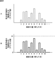
また、シンボルを検出する処理が所定の期間(ソースデータを転送するのに必要な期間)だけ繰り返し実行され、図7に示されるようなシンボル列がシンボル処理部52により取得される。 Further, the symbol detection process is repeatedly executed for a predetermined period (period necessary for transferring the source data), and a symbol string as shown in FIG.
図7に示される例においては、シンボルS1乃至S3は、検出の際に同期をとるためのシンボルであり、単純なパターンからなるシンボルを繰り返すものとされる。そして、シンボルS4乃至Snにより、例えば、画像データ、音楽データ、テキストデータなどの各種のソースデータが表される。 In the example shown in FIG. 7, the symbols S1 to S3 are symbols for synchronization at the time of detection, and a symbol having a simple pattern is repeated. The symbols S4 to Sn represent various source data such as image data, music data, and text data.
図7に示されるようなシンボル列がシンボル処理部52により取得され、データ処理部51に出力される。
A symbol string as shown in FIG. 7 is acquired by the
また、シンボル処理部52は、表示部11の所定の位置にシンボルを表示し、情報処理端末21にデータを転送するとき、データ処理部51から供給されたデータに基づいてシンボルを生成する。シンボル処理部52により生成されたシンボル列のデータは画像信号生成部47に出力される。例えば、シンボル処理部52により、図7のシンボル列が生成された場合、表示部11には、シンボルS1乃至Snのそれぞれが、1フレームの表示毎に順次表示される。
Further, the
データ処理部51は、表示部11にシンボルを表示するとき、制御部45により取得され、供給されたソースデータ(情報処理端末21に転送するデータ)に対して、スクランブル、誤り訂正ブロックの付加、変調処理等を適宜施し、得られたデータをシンボル処理部52に出力する。
When displaying a symbol on the
また、データ処理部51は、表示部11に形成された読み取り領域においてシンボルが検出され、それを表すデータがシンボル処理部52から供給されたとき、供給されたデータに対して復調処理、誤り訂正処理、およびデスクランブル処理等を適宜施し、得られたソースデータ(情報処理端末21から転送されたデータ)を制御部45に供給する。
In addition, when a symbol is detected in the reading area formed on the
制御部45に供給された、情報処理端末21から転送されてきたデータは、記憶部44に記憶されたり、或いは、転送されてきたデータに基づく画像信号生成部47およびコントローラ48の処理により、対応する画像が表示部11に表示される。
The data transferred from the
図8は、情報処理端末21とリーダライタ24の構成例を示すブロック図である。
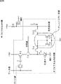
FIG. 8 is a block diagram illustrating a configuration example of the
リーダライタ24の先端面24Aにはレンズ101が配設されており、例えば、表示部11に表示されているシンボルに先端面24Aが当接または近接されたとき、表示部11から出射される、シンボルのパターンを表す光がレンズ101を介してリーダライタ24の内部に入射される。入射された光は、ハーフミラー102で反射され、シンボル検出部103により受光される。
The
シンボル検出部103には、光の有無を検出する光センサがアレイ状に配設されており、ハーフミラー102で反射され、受光された光から、そのとき表示部11に表示されているシンボルが検出される。シンボル検出部103の検出結果は、ケーブル23を介して情報処理端末21のシンボル処理部112に出力される。
In the
シンボル表示部104は、プログレッシブ方式により表示可能なLCDなどから構成され、表示部11と同じ周波数でシンボルを表示する。例えば、表示装置1にデータを転送するとき、シンボル表示部104は、画像信号生成部111から供給された信号に基づいて、転送するデータを表すシンボルを順次表示し、自分自身を挟んでハーフミラー102と対向する位置に設けられている光源(図示せず)からの光を利用して、シンボルを表す光を、表示部11に形成される読み取り領域に照射する。照射された光は、ハーフミラー102およびレンズ101を介してリーダライタ24の先端面24Aから外部に出射される。
The
制御部114は、ROM(図示せず)やハードディスクなどよりなる記憶部118に記憶されている制御プログラムに基づいて、情報処理端末21の全体の動作を制御する。通信部115は、インターネットなどのネットワークを介して、各種の機器と有線または無線により通信を行う。
The
入力部117は、所定の入力ボタンや、表示部22に重畳して配置されるタッチパネルなどに入力されるユーザからの指示を制御部114に出力する。
The input unit 117 outputs an instruction from a user input to a predetermined input button or a touch panel arranged to be superimposed on the
画像信号生成部111は、シンボル処理部112により生成され、供給されたシンボル列のデータに基づいて、シンボル表示部104にシンボルを表示させるための画像信号を生成し、それを、ケーブル23を介してシンボル表示部104に出力する。
The image
シンボル処理部112は、表示装置1からデータを取得するとき、シンボル検出部103による検出結果に基づいてシンボルを復元し、表示部11に表示されたシンボル列を取得する。すなわち、シンボルを検出する処理が所定の期間だけ繰り返し実行され、例えば、図7に示されるようなシンボル列がシンボル処理部112により取得される。
When the
また、シンボル処理部112は、シンボル表示部104にシンボルを表示し、表示装置1にデータを転送するとき、データ処理部113から供給されたデータに基づいてシンボルを生成する。シンボル処理部112により生成されたシンボルのデータは、画像信号生成部111に出力される。
The
データ処理部113は、シンボル表示部104にシンボルを表示するとき、制御部114から供給されたソースデータ(表示装置1に転送するデータ)に対して、スクランブル、誤り訂正ブロックの付加、変調処理等を適宜施し、得られたデータをシンボル処理部112に出力する。また、データ処理部113は、検出されたシンボルを表すデータがシンボル処理部112から供給されたとき、そのデータに対して復調処理、誤り訂正処理、およびデスクランブル処理等を適宜施し、得られたソースデータ(表示装置1から転送されたデータ)を制御部114に供給する。
When displaying a symbol on the
なお、制御部114には、必要に応じてドライブ116が接続され、磁気ディスク131、光ディスク132、光磁気ディスク133、或いは半導体メモリ134などが適宜装着され、それから読み出されたコンピュータプログラムが、必要に応じて記憶部118にインストールされる。
Note that a drive 116 is connected to the
次に、図1の情報処理システムの動作についてフローチャートを参照して説明する。 Next, the operation of the information processing system in FIG. 1 will be described with reference to a flowchart.
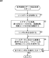
始めに、図9のフローチャートを参照して、情報処理端末21に対してデータを転送する表示装置1の処理について説明する。
First, processing of the
ステップS1において、制御部45は、情報処理端末21に転送するソースデータを取得する。例えば、制御部45は、ユーザからの指示により、所定のテレビジョン番組を表示部11に表示させている状態において、その番組のデータを転送することが指示されたとき、或いは、ネットワークを介して取得した画像データなどを表示部11に表示させている状態において、その画像データを転送することが指示されたとき、その指示に応じて、番組データや画像データをソースデータとして取得する。
In step S <b> 1, the
当然、ユーザは、表示装置1の記憶部44に記憶されている音楽データやテキストデータなど、各種のデータを情報処理端末21に転送することを表示装置1に指示することができる。
Naturally, the user can instruct the
制御部45により取得されたソースデータは、例えば、画像信号生成部47とデータ処理部51に出力される。
The source data acquired by the
ステップS2において、データ処理部51は、制御部45から供給されたソースデータに応じて、シンボル列によりソースデータを表すことができるように、所定の単位のデータ毎に、スクランブル処理、誤り訂正コードの付加、変調処理、および同期コードの付加などを適宜行う。
In step S2, the
また、転送されるデータのタイトルやカテゴリを表す情報、或いは、データ量やデータのフォーマットを表す情報などが、サブデータとして適宜付加される。データ処理部51により各種の処理が施された後に得られたデータは、シンボル処理部52に供給される。
Also, information indicating the title and category of data to be transferred, information indicating the data amount and data format, and the like are appropriately added as sub-data. Data obtained after various processes are performed by the
シンボル処理部52は、ステップS3において、例えば、予め用意されている変換テーブルを参照し、データ処理部51から供給されたデータに対応するシンボルを生成する。生成されるシンボルは、各セルが黒白でコード化されたマトリクス型のシンボルであってもよいし、バーコードが積み重ねられてコード化されたスタック型のシンボルであってもよい。
In step S3, the
ソースデータのデータ量に対応する所定の数のシンボルがシンボル処理部52により生成され、例えば、図7に示されるようなシンボル列が画像信号生成部47に出力される。
A predetermined number of symbols corresponding to the data amount of the source data is generated by the
ステップS4において、画像信号生成部47は、制御部45から供給されたソースデータに対応する画像を表示させるための画像信号と、シンボル処理部52から供給されたシンボル列を表示させるための画像信号を重畳して得られた画像信号をコントローラ48に供給し、ソースデータに対応する画像とともにシンボルを順次表示させる。
In step S4, the image
これにより、表示されている画像に対応するシンボル(表示されている画像を転送するためのシンボル)が、例えば、画像の近傍などの、表示部11の所定の位置に表示される。
Thereby, a symbol corresponding to the displayed image (a symbol for transferring the displayed image) is displayed at a predetermined position of the
ステップS5において、コントローラ48は、転送するデータを表す全てのシンボルを表示したか否かを判定し、全てのシンボルを表示したと判定するまで、ステップS4に戻り、シンボルの表示を順次繰り返す。その後、ステップS5において、全てのシンボルを表示したと判定された場合、処理が終了される。
In step S5, the
なお、表示されているシンボルを取り込むことで、そのとき表示部11に表示されている画像データを情報処理端末21に取り込むことができることをユーザが認識できるように、転送するデータによる画像が表示されている期間だけ、シンボル列が繰り返し表示されるようにしてもよい。例えば、10分間の動画像が表示部11に表示されている場合、その動画像のデータから生成されたシンボル列が、画像の表示に併せて10分間繰り返し表示される。
By capturing the displayed symbol, an image of the data to be transferred is displayed so that the user can recognize that the image data displayed on the
以上のようにして表示部11の所定の位置に表示されるシンボルをリーダライタ24で読み取ることにより、ユーザは、表示装置1から情報処理端末21にデータを取り込むことができる。
By reading the symbol displayed at the predetermined position of the
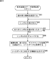
次に、図10のフローチャートを参照して、図9の処理に対応して実行される、情報処理端末21のデータ取得処理について説明する。
Next, a data acquisition process of the
リーダライタ24の先端面24Aが表示部11に当接され、当接された位置に表示されているシンボルの同期コード(図7)を検出したとき、シンボル検出部103は、ステップS21において、それを読み取る。
When the
ステップS22において、シンボル検出部103は、全てのシンボルを読み取ったか否かを判定し、読み取っていないと判定した場合、ステップS21に戻り、表示されるシンボルを繰り返し読み取る。シンボル検出部103により読み取られたシンボルの情報は、例えば、シンボル処理部112に順次出力される。
In step S22, the
シンボル検出部103は、例えば、シンボル列の終端のシンボルであることを表すシンボルを検出したとき、ステップS22において、転送されるデータを表す全てのシンボルを読み取ったと判定する。
For example, when the
ステップS23において、シンボル処理部112は、シンボル列をデコードし、得られたデータをデータ処理部113に出力する。データ処理部113は、シンボル処理部112から供給されたデータに対して、復調処理、誤り訂正処理、デスクランブル処理等をステップS24において適宜行い、ソースデータを取得する。これにより、表示装置1において、情報処理端末21に転送するものとして選択されたソースデータが情報処理端末21により取得される。
In step S23, the
ステップS25において、制御部114は、データ処理部113により取得されたソースデータに対応する処理を行う。
In step S <b> 25, the
例えば、図11に示されるように、ウインドウ151に、動画像151Aと、動画像151Aのデータを表すシンボル152が表示され(図9の処理)、ユーザがリーダライタ24によりシンボル152を読み取らせた場合、動画像151Aのソースデータが情報処理端末21に転送され(図10のステップS21乃至S24の処理)、制御部114は、ステップS25において、転送されたソースデータに基づいて、動画像を表示部22に表示させる。
For example, as shown in FIG. 11, the moving
これにより、ユーザは、ウインドウ151に表示されているものと同一の画像を、表示部22に表示させることができ、表示装置1と離れた場所でも、情報処理端末21を用いて、動画像151Aの内容を確認することができる。
Thereby, the user can display the same image as that displayed on the
また、情報処理端末21に転送されたソースデータは、ステップS25において、記憶部118に保存されたり、通信部115を介して他の機器に送信されたり、或いは、ドライブ116に装着された記録媒体に記録される。
Further, the source data transferred to the
さらに、図11のウインドウ161に、例えば、ネットワークを介して取得されたテキスト画像161Aが表示され(図9の処理)、ユーザがウインドウ161の右隅に表示されているシンボル162をリーダライタ24により読み取らせた場合、テキストデータ(ソースデータ)が情報処理端末21に転送される(図10のステップS21乃至S24の処理)。
Further, for example, a
制御部114は、ステップS25において、転送されたテキストデータを記憶部118に保存させたり、或いは、対応する画像(テキスト画像)を表示部22に表示させる。
In step S25, the
図11のウインドウ171に表示されるシンボル172は、音楽データをソースデータとして生成され、表示されるものであり(図9の処理)、シンボル172にリーダライタ24が所定の期間(音楽データのデータ量に対応するシンボルが表示される期間)だけ当接されたとき、情報処理端末21により音楽データが取り込まれる(図10のステップS21乃至S24の処理)。取り込まれた音楽データは、例えば、図10のステップS25において再生され、情報処理端末21の図示せぬスピーカから出力される。
The
なお、ウインドウ171には、情報処理端末21に取り込むことができる音楽のタイトルやアーティストに関する情報などのサブデータが表示されるようにしてもよい。
Note that the
例えば、テレビジョン番組において音楽が流れると同時にウインドウ171とシンボル172が表示部11の所定の位置に表示される場合、ユーザは、表示されるシンボル172をリーダライタ24で読み取らせることにより、その音楽データを情報処理端末21に取り込むことができる。
For example, when music flows in a television program and the
また、ソースデータとして、所定のサイトにアクセスするためのURLが取得された場合、ウインドウ181には、そのURLを表すシンボル182が表示される(図9の処理)。リーダライタ24がシンボル182に当接され、URLが制御部114により取得された場合、制御部114は、ステップS25において、通信部115を制御して、取得したURLにより指定されるサイトにアクセスし、アクセスしたサイトの画面を表示部22に表示させる。
When a URL for accessing a predetermined site is acquired as source data, a
当然、ウインドウ181にサイトの画面がシンボル182とともに表示されており、そのシンボル182を読み取らせることで、情報処理端末21においてもサイトの画面を確認できるようにしてもよい。
Naturally, the screen of the site is displayed in the
以上のように、ユーザは、表示されるシンボルをリーダライタ24により読み取らせるだけでよいため、直感的かつ容易な操作により、各種のデータを情報処理端末21に取り込むことができる。
As described above, since the user only needs to read the displayed symbol with the reader /
次に、図12および図13のフローチャートを参照して、図9および図10を参照して説明したものと反対に、情報処理端末21から表示装置1に対してデータを転送する情報処理システムの動作について説明する。
Next, referring to the flowcharts of FIGS. 12 and 13, the information processing system for transferring data from the
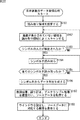
始めに、図12のフローチャートを参照して、表示装置1にデータを転送する情報処理端末21の処理について説明する。
First, the processing of the
図12に示される処理は、図9を参照して説明した表示装置1の処理と基本的に同様の処理である。すなわち、制御部114は、ステップS41において、表示装置1に転送するソースデータを取得する。例えば、ユーザの入力部117に対する入力により、記憶部118に記憶されている所定のデータを転送することが指示されたとき、或いは、ネットワークを介して取得した画像データなどを表示部22に表示させている状態において、その画像データを転送することが指示されたとき、制御部114は、その指示に応じてソースデータを取得する。
The process shown in FIG. 12 is basically the same as the process of the
ステップS42において、データ処理部113は、制御部114から供給されたソースデータに応じて、シンボル列によりソースデータを表すことができるように、所定の単位のデータ毎に、スクランブル処理、誤り訂正コードの付加、変調処理、および同期コードの付加などを適宜行う。
In step S42, the
シンボル処理部112は、ステップS43において、例えば、予め用意されている変換テーブルを参照し、データ処理部113から供給されたデータに対応するシンボル列を生成する。生成されたシンボル列は、画像信号生成部111に出力される。
In step S43, the
ステップS44において、画像信号生成部111は、シンボル処理部112から供給されたシンボル列のデータに基づいて、シンボルを表示させるための画像信号を生成し、シンボル表示部104に順次表示させる。
In step S <b> 44, the image
シンボル表示部104においては、例えば、表示装置1の表示部11と同じ周波数でシンボル列のそれぞれのシンボルが順次表示され、シンボルを表す光がハーフミラー102およびレンズ101を介してリーダライタ24の外部に出射される。
In the
後述するように、リーダライタ24の先端面24Aが表示部11に形成される読み取り領域に当接されているとき、ステップS44において表示されるシンボル(リーダライタ24から出射されるシンボルを表す光)が読み取り領域において読み取られる(図13のステップS62)。
As will be described later, when the
画像信号生成部111は、ステップS45において、転送するデータを表すシンボル列の各シンボルを、シンボル表示部104に全て表示したか否かを判定し、表示していないと判定した場合、ステップS44に戻り、シンボルの表示を繰り返す。画像信号処理部111は、ステップS45において、全てのシンボルを表示したと判定した場合、処理を終了させる。
In step S45, the image
次に、図13のフローチャートを参照して、図12の処理に対応して実行される、表示装置1のデータ取得処理について説明する。
Next, a data acquisition process of the
ステップS61において、制御部45は、表示部11の所定の位置に読み取り領域を設定する。すなわち、制御部45は、所定の画素(TFT)に逆方向のバイアス電圧を印加し、読み取り領域を表示部11に形成する。
In step S <b> 61, the
読み取り領域は、所定の位置に固定的に常時形成されるようにしてもよいし、それまで正方向のバイアス電圧が印加されており、シンボルが表示されていた位置に形成されるようにしてもよい。 The reading area may be always formed fixedly at a predetermined position, or may be formed at a position where a positive bias voltage has been applied and the symbol has been displayed. Good.
形成された読み取り領域にリーダライタ24の先端面24Aが当接され、リーダライタ24のシンボル表示部104に表示されているシンボルを表す光が照射されたとき、シンボル処理部52は、ステップS62において、検出部53による検出結果に基づいてシンボルを読み取る。
When the
上述したように、シンボル処理部52は、読み取り領域を構成するそれぞれの画素においてリーク電流が検出された場合、その画素の正面にはシンボルの白の領域があるものとし、一方、リーク電流が検出されていない場合、その画素の正面にはシンボルの黒の領域があるとものして、読み取り領域を構成する各画素の検出結果を合成し、1つのシンボルを読み取る。
As described above, when a leak current is detected in each pixel constituting the reading area, the
シンボル処理部52は、ステップS63において、全てのシンボルを読み取ったか否かを判定し、読み取っていないと判定した場合、ステップS62に戻り、リーダライタ24において出力されるシンボルを繰り返し読み取る。検出部53により読み取られたシンボルの情報は、シンボル処理部52に順次出力される。
In step S63, the
シンボル処理部52は、ステップS63において、シンボル列の終端であることを表すシンボルが検出されたとき、転送されるデータを表す全てのシンボルを読み取ったと判定し、ステップS64に進む。
When the symbol representing the end of the symbol string is detected in step S63, the
ステップS64において、シンボル処理部52は、2次元コードのパターンと、データの対応テーブルを参照してシンボル列をデコードし、得られたデータをデータ処理部51に出力する。
In step S <b> 64, the
データ処理部51は、ステップS65において、シンボル処理部52から供給されたデータに対して、復調処理、誤り訂正処理、デスクランブル処理等を適宜行い、ソースデータを取得する。これにより、情報処理端末21において選択されたソースデータが表示装置1により取得された状態になる。
In step S65, the
ステップS66において、制御部45は、データ処理部51により取得されたソースデータに対応する処理を行う。
In step S <b> 66, the
例えば、図12に示されるように、情報処理端末21の表示部22に表示されている動画像22Aが、表示装置1に転送するデータとして選択された場合、動画像22Aを表すシンボル列が生成され、リーダライタ24から、各シンボルを表す光が順次出射される(図12のステップS44)。
For example, as shown in FIG. 12, when a moving
そして、リーダライタ24から出射されるシンボル列が、表示部11の右下方に形成される読み取り領域192において読み取られた場合(図13のステップS62)、ウインドウ191が表示され、そこに、読み取られたシンボル列から取得されたソースデータ(動画像22Aのデータ)に対応する動画像が表示される(図13のステップS66)。
When the symbol string emitted from the reader /
このように、ユーザは、情報処理端末21において指定し、リーダライタ24を読み取り領域192に当接させるだけで、指定した画像を表示部11に拡大表示させることができる。例えば、情報処理端末21がPDAなどの端末である場合、表示部22の大きさが制限されることから、画像の詳細を確認することが困難である場合があるが、以上のようにして、情報処理端末21から表示装置1にデータを転送し、表示部11に画像を拡大表示させることで、その詳細を容易に確認することができる。
In this way, the user can enlarge and display the designated image on the
同様にして、情報処理端末21において選択された音楽データが表示装置1に転送されたとき、表示装置1により音楽データが再生され、再生音がスピーカから出力される。
Similarly, when the music data selected in the
また、情報処理端末21において指定されたURLが表示装置1に転送されたとき、表示装置1により、そのURLにより指定されるサイトに対するアクセスが通信部43を介して行われ、アクセスしたサイトの画面が表示部11に表示される。
When the URL specified in the
以上においては、単にデータのみが送受信されるとしたが、取得されたデータに対する処理の内容を指示する命令コード(指示情報)がシンボル列に含まれている場合、そのシンボル列を読み取った機器により、命令コードに応じて各種の処理が実行されるようにしてもよい。 In the above, it is assumed that only data is transmitted / received. However, when an instruction code (instruction information) for instructing the content of processing for the acquired data is included in the symbol string, it is determined by the device that has read the symbol string. Various processes may be executed according to the instruction code.
次に、図15のフローチャートを参照して、命令コードを含むシンボル列を表示し、データを表示装置1に転送する情報処理端末21の処理について説明する。
Next, processing of the
図15に示される処理は、ユーザからの入力に基づいて命令コードを生成し、それをソースデータに付加する処理が行われる点を除いて、基本的に、図12のステップS41乃至S45の処理と同様の処理であり、詳細な説明は省略する。 The process shown in FIG. 15 is basically the process of steps S41 to S45 in FIG. 12 except that an instruction code is generated based on an input from the user and is added to the source data. The detailed processing is omitted.
すなわち、制御部114は、ステップS81において、ソースデータを取得したとき、ステップS82に進み、取得したソースデータに命令コードを付加する。例えば、命令コードとして、命令コードとともに転送されたソースデータの画像を表示するウインドウの大きさ、表示位置、表示時間などを指示するコードや、命令コードとともに転送されたソースデータに、その転送主(ユーザ)のみが表示装置1において再生できるような鍵を設定することを指示するコードなどがユーザからの指示に基づいて付加される。
That is, when the
ステップS83において、データ処理部113により、命令コードが付加されたソースデータに各種の処理が施される。また、各種の処理が施されて得られたデータに基づいて、ステップS84において、シンボル処理部112によりシンボル列が生成される。
In step S83, the
そして、ステップS85において、各シンボルがシンボル表示部104に順次表示され、全てのシンボルが表示されたとき、処理が終了される。
In step S85, each symbol is sequentially displayed on the
次に、図16のフローチャートを参照して、図15の処理に対応して実行される、表示装置1のデータ取得処理について説明する。
Next, a data acquisition process of the
ステップS101乃至S105の処理は、図13のステップS61乃至S65の処理と同様の処理であるため、その説明は省略する。すなわち、表示部11に形成した読み取り領域においてシンボル列を読み取り、ソースデータを取得したとき、ステップS106において、表示装置1の制御部45は、取得したデータから命令コードを抽出する。
The processing in steps S101 to S105 is the same as the processing in steps S61 to S65 in FIG. That is, when the symbol string is read in the reading area formed on the
ステップS107において、制御部45は、抽出した命令コードに基づいて画像信号生成部47を制御し、ソースデータに対応する画像の表示を制御する。
In step S107, the
例えば、命令コードとして、表示部11の所定の位置にウインドウを表示し、そこに、ソースデータに対応する画像を表示させることを指示するコードを抽出した場合、制御部45は、そのコードに従ってウインドウの表示位置を決定する。また、制御部45は、命令コードとしてウインドウのサイズを指示するコードも含まれている場合、指示されるサイズのウインドウを表示し、ソースデータに対応する画像を表示する。
For example, when a window is displayed as a command code at a predetermined position on the
さらに、制御部45は、命令コードとして、ソースデータに対応する画像を表示する期間を指示するコードを抽出した場合、それにより指定された時刻までソースデータに対応する画像を表示し続ける。
Further, when the
このように、ユーザは、情報処理端末21において表示の設定を行い、その設定通りに、表示装置1に画像を表示させることができる。
Thus, the user can set display on the
同様に、転送するデータが音楽データである場合、その音楽データを再生するときの音量を指示するコードや、再生モード(リピート再生、シャッフル再生等)などを指示するコードが命令コードとして含まれ、その命令コードに従って、表示装置1において音楽データが再生される。
Similarly, when the data to be transferred is music data, a code for instructing a volume when reproducing the music data, a code for instructing a reproduction mode (repeat reproduction, shuffle reproduction, etc.), etc. are included as instruction codes. Music data is reproduced on the
図17は、図15の処理に対応して実行される、表示装置1の他のデータ取得処理について説明するフローチャートである。
FIG. 17 is a flowchart for explaining another data acquisition process of the
この例においては、ソースデータを表示装置1に転送した本人のみが、そのソースデータを表示装置1において再生できるようにすることを指示するコードが、命令コードとして、ソースデータとともに情報処理端末21から表示装置1に転送される。
In this example, only the person who transferred the source data to the
ステップS121乃至S126の処理は、図16のステップS101乃至S106の処理と同様の処理であるため、その説明は省略する。すなわち、読み取り領域において読み取ったシンボル列からソースデータを取得し、命令コードを抽出したとき、ステップS127において、表示装置1の制御部45は、取得したデータを記憶部44に保存し、保存したデータに鍵を設定する。
The processing in steps S121 to S126 is the same as the processing in steps S101 to S106 in FIG. That is, when the source data is acquired from the symbol string read in the reading area and the instruction code is extracted, the
例えば、情報処理端末21からの命令コードには、情報処理端末21に固有のものとして設定される識別情報が含まれており、その識別情報と組み合わせることで鍵を解くことができるシンボルを生成し、表示部11に表示させる。表示部11に表示されたシンボルと、情報処理端末21の識別情報を組み合わせることで生成できる解読シンボルは、保存することが指示されたデータと対応付けて記憶部44に保存される。
For example, the instruction code from the
情報処理端末21から転送されたデータに鍵が設定されたとき、表示部11には、図18に示されるような画面が表示される。
When a key is set in the data transferred from the
例えば、ユーザAが利用する情報処理端末21からデータが転送され、そのデータに鍵を設定することが命令コードにより指示されたとき、制御部45は、情報処理端末21の識別情報と組み合わせることで解読シンボルを生成できるシンボル201を、ユーザ名(ユーザA)の直右方に表示させる。なお、ユーザ名は、命令コードに含まれる情報に基づいて表示されるものである。
For example, when data is transferred from the
従って、ユーザは、表示装置1に転送し、保存しておいたデータを再生するとき、リーダライタ24によりシンボル201を読み取り、情報処理端末21に、鍵を解くための解読シンボルを生成させる。
Therefore, when the user transfers the data transferred to the
例えば、シンボル201が表示されている位置には、所定の周期で読み取り領域が設定されるため(シンボル201が表示されている画素に印加されるバイアス電圧の極性が所定の周期で切り換えられるため)、ユーザは、新たに形成される読み取り領域に、情報処理端末21において生成させた解読シンボルをリーダライタ24から入力し、保存しておいたデータを再生(出力)させる。
For example, a reading area is set at a predetermined cycle at a position where the
なお、シンボルの表示と読み取り領域の形成が周期的に切り換えられるのではなく、例えば、図18のシンボル201の近傍に読み取り領域が常時設定されているようにしてもよい。
It should be noted that the symbol display and the reading area formation are not periodically switched, but for example, the reading area may be always set in the vicinity of the
図17の説明に戻り、ステップS128において、制御部45は、データ処理部51からの出力に基づいて、解読シンボルが読み取り領域において読み取られたか否かを判定し、読み取られたと判定するまで待機する。上述したようにして、情報処理端末21において生成された解読シンボルが読み取り領域に入力されたとき、検出部53により検出された解読シンボルを表すデータが、シンボル処理部52およびデータ処理部51を介して制御部45に供給される。
Returning to the description of FIG. 17, in step S128, the
制御部45は、ステップS128において、解読シンボルが供給されたと判定した場合、ステップS129に進み、供給された解読シンボルに対応付けて保存されているデータを記憶部44から読み出し、再生する。例えば、保存されていたデータが画像データである場合、対応する画像が表示部11に表示され、保存されていたデータが音楽データである場合、その音楽データが再生される。
If it is determined in step S128 that the decoded symbol has been supplied, the
以上のように、自分自身の名前の近傍に表示されるシンボルをリーダライタ24により読み取り、それに応じて生成された解読シンボルを表示装置1に入力することで、保存しておいたデータを再生させることができるため、ユーザは、直感的な操作で、データを保存することができるとともに、その再生を指示することができる。
As described above, the symbol displayed in the vicinity of the user's own name is read by the reader /
なお、図18の例においては、ユーザBが使用する端末から転送されたデータと、ユーザCが使用する端末から転送されたデータに対しても鍵が設定されていることが表示されている。 In the example of FIG. 18, it is displayed that the key is set for the data transferred from the terminal used by the user B and the data transferred from the terminal used by the user C.
仮に、ユーザAが情報処理端末21のリーダライタ24によりシンボル202(ユーザBが使用する端末の識別情報と組み合わせることで解読シンボルを生成することができるシンボル)を読み取った場合であっても、ユーザBの端末の識別情報が情報処理端末21には用意されていないため、ユーザAは、ユーザBにより保存され、鍵が設定されたデータを再生させることができない。
Even if the user A reads the symbol 202 (a symbol that can generate a decoded symbol by combining with the identification information of the terminal used by the user B) by the reader /
従って、自分が保存していたデータが他人に利用されることを防止することができる。なお、以上においては、端末の識別情報と、表示されるシンボルに基づいて解読シンボルが生成され、それにより鍵を解除することができるとしたが、鍵の設定と解読のアルゴリズムは適宜変更可能である。 Therefore, it is possible to prevent data stored by the user from being used by others. In the above description, the decryption symbol is generated based on the terminal identification information and the displayed symbol, and thus the key can be released. However, the key setting and decryption algorithm can be changed as appropriate. is there.
次に、図19のフローチャートを参照して、図15の処理に対応して実行される、表示装置1のさらに他のデータ取得処理について説明する。
Next, still another data acquisition process of the
この例においては、指定する機器にデータを送信することを指示するコードが、命令コードとして情報処理端末21から表示装置1に転送される。例えば、機器を指定する情報であるアドレスなどが命令コードに含まれ、その命令コードが、アドレスで指定する機器に送信するデータとともに転送される。
In this example, a code instructing to transmit data to a designated device is transferred from the
ステップS141乃至S146の処理は、図16のステップS101乃至S106の処理と同様の処理であるため、その説明は省略する。すなわち、読み取り領域において読み取ったシンボル列からソースデータを取得し、命令コードを抽出したとき、ステップS147において、表示装置1の制御部45は、命令コードにより指定される機器に、取得したデータを送信する。
The processing in steps S141 to S146 is the same as the processing in steps S101 to S106 in FIG. That is, when the source data is acquired from the symbol string read in the reading area and the instruction code is extracted, in step S147, the
例えば、情報処理端末21において入力された、ネットワークを介して接続される機器のアドレスが命令コードに含まれている場合、制御部45は、通信部43を制御し、情報処理端末21から転送されたデータを、そのアドレスで指定される機器に送信する。
For example, when the instruction code includes an address of a device connected via the network that is input at the
これにより、ユーザは、情報処理端末21に通信部115が設けられていない場合であっても、情報処理端末21において送信先の機器を指定し、リーダライタ24を表示部11に当接させるだけで、表示装置1を介して、他の機器にデータを送信することができる。
As a result, even when the
以上においては、命令コードとして、画像の表示を制御する情報、送信したデータに鍵を設定することを指示する情報、および、データの送信先を指定する情報などが含まれるとしたが、これ以外にも、各種の情報を命令コードに含めることができるようにしてもよい。 In the above, the instruction code includes information for controlling image display, information for instructing to set a key for transmitted data, and information for specifying a data transmission destination. In addition, various kinds of information may be included in the instruction code.
例えば、データの属性を表す情報を命令コードとしてデータとともに転送し、その命令コードを取得した機器において、命令コードに応じた処理が行われるようにしてもよい。データの属性を表す情報として、それぞれのデータの優先度が含まれている場合、優先度に応じて、表示される順番が制御されたり、或いは、それぞれのデータの表示サイズが制御される。また、データの属性を表す情報として、ユーザの嗜好情報(視聴履歴情報)が含まれている場合、ユーザの嗜好に応じて、表示される順番や表示位置などが制御される。 For example, information representing the attribute of data may be transferred together with data as an instruction code, and processing corresponding to the instruction code may be performed in a device that has acquired the instruction code. When the priority of each data is included as information representing the attribute of the data, the display order is controlled according to the priority, or the display size of each data is controlled. When user preference information (viewing history information) is included as information representing data attributes, the display order, display position, and the like are controlled according to the user preference.
以上においては、読み取り領域は、表示部11の所定の位置に固定して形成されるか、または、シンボルが表示される位置に周期的に形成される場合について説明したが、表示部11の走査に併せて、読み取り領域の移動が行われるようにしてもよい。
In the above description, the case where the reading area is fixedly formed at a predetermined position of the
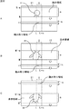
例えば、図20の点線矢印で示されるように、表示部11の画面走査が画面の左上端から1/60(秒)の周期で行われる場合、この走査に併せて逆方向の電圧が印加される画素が切り換えられることで読み取り領域211の移動が行われる。これにより、表示部11にリーダライタ24が当接されたか否かが、1/60(秒)の周期でスキャンされることになる。
For example, as shown by the dotted arrow in FIG. 20, when the screen scan of the
なお、表示部11にウインドウ212が既に表示されている場合、画像の表示と同時に、読み取り領域として1つの画素(ウインドウ212の画素)を機能させることができないため、ウインドウ212が表示される領域以外の領域で、読み取り領域211によるスキャンが行われる。
When the
例えば、図21に示される表示部11の位置Pにユーザがリーダライタ24を当接させているときに、読み取り領域211により位置Pがスキャンされた場合、リーダライタ24から出力されるシンボルが読み取り領域211により読み取られ、情報処理端末21において選択されたデータが表示装置1に転送される。
For example, if the position P is scanned by the
データが表示装置1に転送されたとき、例えば、読み取り領域211が右隅に位置するように、ウインドウ221が表示され、そこに、取り込まれたデータに対応する画像が表示される。
When the data is transferred to the
このように表示部11の表面にリーダライタ24が当接されたか否か(データの転送が行われるか否か)が周期的にスキャンされ、当接された位置を基準としてウインドウが表示されるようにしたため、ユーザは、画像が表示されていない領域であれば、リーダライタ24を移動させやすい位置、或いは、ウインドウを表示させたい位置、すなわち、好みの位置にリーダライタ24を当接させることでデータを表示装置1に転送することができる。
As described above, whether the reader /
次に、図22のフローチャートを参照して、図20および図21に示されるように、リーダライタ24からの入力の有無を読み取り領域によりスキャンし、リーダライタ24が当接されたときに情報処理端末21からデータを取得する表示装置1の処理について説明する。
Next, referring to the flowchart of FIG. 22, as shown in FIGS. 20 and 21, the presence / absence of input from the reader /
ステップS161において、制御部45は、所定の画素に逆方向のバイアス電圧を印加して読み取り領域を設定し、ステップS162に進み、画像が表示されていない領域を、設定した読み取り領域によりスキャンする。
In step S161, the
ステップS163において、制御部45は、リーダライタ24が表示部11の表面に当接され、シンボルの入力が読み取り領域において検出されたか否かを判定し、検出されていないと判定した場合、ステップS162に戻り、スキャンを繰り返す。
In step S163, the
一方、読み取り領域において、リーク電流が発生されたことが検出され、シンボルが入力されたと判定した場合、制御部45は、読み取り領域の移動を停止し、ステップS164に進み、シンボルを読み取る。
On the other hand, when it is detected that a leak current has occurred in the reading area and it is determined that a symbol has been input, the
すなわち、ステップS164乃至S167において、上述した処理と同様のシンボルの読み取り処理が実行され、ソースデータが取得される。ソースデータが取得されたとき、制御部45は、ステップS168において、リーダライタ24が当接された位置を基準としてウインドウを表示させ、そこに、転送されてきたデータに対応する画像を表示させる。
That is, in steps S164 to S167, a symbol reading process similar to the process described above is executed, and source data is acquired. When the source data is acquired, in step S168, the
以上の処理により、ユーザは、所定の位置に固定して設定されている読み取り領域にリーダライタ24を当接させることなく、好みの位置に、かつ、容易に、データを表示装置1に転送することができる。
Through the above processing, the user can easily transfer the data to the
なお、図20および図21に示される例においては、説明の便宜上、比較的広い範囲に読み取り領域が形成され、それが移動されるとしたが、1画素からなる読み取り領域により順次スキャンが行われるようにしてもよい。 In the example shown in FIG. 20 and FIG. 21, it is assumed that the reading area is formed and moved in a relatively wide range for convenience of explanation, but scanning is sequentially performed by the reading area consisting of one pixel. You may do it.
この場合、スキャンが行われる1画素によりシンボルの入力が検出されたとき、検出された位置の周囲の所定の範囲に読み取り領域が拡大して設定され(検出された位置の周囲の画素の極性が切り換えられ)、設定された読み取り領域により、リーダライタ24から出射されるシンボルが読み取られる。
In this case, when the input of the symbol is detected by one pixel to be scanned, the reading area is set to be enlarged to a predetermined range around the detected position (the polarity of the pixel around the detected position is set). The symbols emitted from the reader /
ユーザからの入力の有無を検出する画素は、必要最小限の1画素だけでよいため、これにより、その1画素を除く、他の全ての画素に画像を表示させることができる。従って、ユーザからの入力を順次スキャンする場合であっても、より広い領域を表示領域として確保することができる。 Since only the minimum necessary pixel for detecting the presence or absence of input from the user is required, an image can be displayed on all other pixels except the one pixel. Therefore, even when the input from the user is sequentially scanned, a wider area can be secured as the display area.
以上においては、情報処理端末21には、シンボルの読み書きのみを行うリーダライタ24がケーブル23を介して接続されるとしたが、表示部22が、表示装置1の表示部11と同様にTFTが各画素に配置された表示デバイスにより構成され、その極性を制御することで画像を表示するだけでなく、外部からの光を検出できるセンサ(読み取り領域)として駆動することが可能である場合、リーダライタ24が情報処理端末21に設けられている必要はない。
In the above description, the
図23は、表示装置1の表示部11と同様に、TFTが各画素に配置された表示デバイスが設けられる情報処理端末231の外観を示している。このように、リーダライタが設けられていない場合であっても、表示装置1の表示部11に情報処理端末231の表示部232を当接または近接させることで、上述したようにして、表示装置1と情報処理端末231との間でデータの送受信を実行させることが可能である。
FIG. 23 shows the appearance of the
すなわち、ユーザは、情報処理端末231の表示部232に表示させたシンボルを、表示装置1の表示部11に形成される読み取り領域に読み取らせることにより、情報処理端末231から表示装置1にデータを転送することができる。
That is, the user reads data from the
また、ユーザは、反対に、逆方向のバイアス電圧が印加され、外部からの光を検出するセンサとして駆動するように形成された表示部232の読み取り領域で、表示装置1の表示部11に表示されるシンボルを読み取らせることにより、表示装置1から情報処理端末231にデータを転送することができる。
On the contrary, the user applies a reverse bias voltage and displays on the
従って、情報処理端末231は、ユーザが容易にその位置や向きを変えることができるような大きさの端末とされる。
Therefore, the
以上においては、表示装置1の表示部11は、TFTが各画素に配置されたELディスプレイまたはLCDであるとしたが、図24に示されるように、表示部242のうちの領域243がPDP(Plasma Display Panel)として構成され、領域244が、TFTが各画素に配置されるLCDとして構成されるハイブリッド型のディスプレイであってもよい。
In the above description, the
この場合、表示装置241は、画像の表示のみを行う場合(外部から入力されるシンボルの検出を行わない場合)、PDPからなる領域243とLCDからなる領域244に、すなわち、表示部242全体に画像を表示し、一方、外部から入力されるシンボルを検出する読み取り領域を形成する必要があるとき、領域244の所定の領域の画素に逆方向のバイアス電圧を印加し、読み取り領域を形成する。
In this case, when only displaying an image (when not detecting a symbol input from the outside), the
これにより、TFTが各画素に配置されるELディスプレイやLCDにより表示部242の全体を構成する場合に較べて、容易に、上述したようにして各種のデータを送受信することができる表示装置の大画面化を図ることができる。
Accordingly, as compared with the case where the
また、PDPからなる領域243にのみ画像が表示され、領域244の全体には、外部からの光の有無を検出する光センサがアレイ状に常時配置されるようにしてもよい。この場合、当然、領域244には、画像が表示されない。
In addition, an image may be displayed only in the
さらに、表示装置の縁(表示部が形成されていない部分)や、表示装置の側面などの所定の位置に光センサが設けられ、そこでシンボルが検出されるようにしてもよいし、シンボルの読み書きを行うための小型のTFTディスプレイ(TFTが各画素に配置されたELディスプレイ、LCD)が設けられ、そこでシンボルの表示と検出が行われるようにしてもよい。 Furthermore, a light sensor may be provided at a predetermined position such as an edge of the display device (a portion where the display portion is not formed) or a side surface of the display device, and a symbol may be detected there, or reading / writing of the symbol may be performed. A small TFT display (EL display or LCD in which the TFT is arranged in each pixel) may be provided, and symbol display and detection may be performed there.
シンボルの読み書きを行うための小型のTFTディスプレイが情報処理端末に設けられる場合、その外観構成は、例えば、図25に示されるものとなる。 When a small-sized TFT display for reading and writing symbols is provided in the information processing terminal, the appearance configuration is as shown in FIG. 25, for example.
図25に示される情報処理端末251には、表示部252が筐体の正面に設けられ、表示部252の直右側には、図の垂直方向を軸として回動自在なリーダライタ部253が形成され、そこに、TFTディスプレイ254が設けられている。
In the
例えば、外部の機器に対してシンボルを介してデータを転送する場合、TFTディスプレイ254には、シンボルが順次連続して表示され、シンボルに対応する光が外部に照射される。また、外部の機器に表示されているシンボルを検出する場合、TFTディスプレイ254の各画素には逆方向のバイアス電圧が印加され、光センサとしての駆動が行われる。
For example, when data is transferred to an external device via a symbol, the symbols are sequentially displayed on the
このように、リーダライタ部253が情報処理端末251の筐体に対して回動自在に形成されている場合、表示部252とTFTディスプレイ254の正面を、それぞれ異なる方向に位置させることができるため、ユーザは、表示部252の表示を確認しながら、転送するデータを選択し、表示部252と反対方向に向けられているTFTディスプレイ254の表示によりデータを転送することができる。
As described above, when the reader /
また、図26に示されるように、図1のリーダライタ24の内部に、小型のTFTディスプレイ262が配置され、それにより、シンボルの表示と検出が行われるようにしてもよい。
Further, as shown in FIG. 26, a
以上においては、TFTが各画素に配設されたLCDによっても、逆方向のバイアス電圧を印加することで、外部からの光を検出できるセンサとして駆動させることができるとしたが、仮に、その検出の際にバックライトからの光が誤検出を引き起こすおそれがあるとき、或いは、外部から照射されるシンボルを検出することができないときは、外部からの光を検出するときだけ、バックライトの出力がオフにされるようにしてもよい。 In the above, it is said that the TFT with TFTs arranged in each pixel can be driven as a sensor that can detect light from the outside by applying a reverse bias voltage. If there is a risk that the light from the backlight may cause a false detection at the time, or the symbol irradiated from the outside cannot be detected, the output of the backlight is only detected when the light from the outside is detected. It may be turned off.
これにより、TFTが各画素に配設されたLCDによっても、バックライトの影響を受けることなく、外部からの光を検出できるセンサとして駆動させることができ、シンボルを介して各種のデータの送受信を行わせることが可能となる。 As a result, an LCD with a TFT installed in each pixel can be driven as a sensor that can detect light from the outside without being affected by the backlight, and various data can be sent and received via symbols. It is possible to make it happen.
以上のようにして行われるデータの送受信は、例えば、パーソナルコンピュータ、携帯電話機、PDA、テレビジョン受像機、音楽再生機、ディジタルカメラ、ビデオカメラなどの、表示部が設けられる様々な情報処理装置に実行させることができる。 Data transmission / reception performed as described above is performed on various information processing apparatuses provided with a display unit such as a personal computer, a mobile phone, a PDA, a television receiver, a music player, a digital camera, and a video camera. Can be executed.
ここで、画像の表示と、外部からの入力の検出とを切り替える動作について、より具体的に説明する。 Here, the operation of switching between image display and external input detection will be described more specifically.
図27は、表示装置1の他の構成例を示す図である。図3と同じ部分には同一の符号を付してあり、重複する説明については適宜省略する。
FIG. 27 is a diagram illustrating another configuration example of the
切替部301は、コントローラ48による制御に基づいて、各画素に設けられるスイッチ(TFT)のオン/オフを切り替え、各画素を、画像を表示する画素として、または、外部からの入力を検出する画素として駆動させる。すなわち、上述した構成においては、画像を表示する画素として、または、外部からの入力を検出する画素として駆動させることの切り替えは、TFTのゲート電極に印加する電圧の方向が切り替えられることで行われるものとしたが、この例においては、切替部301によるスイッチの切り替えに応じて行われる。切替部301によるスイッチのオン/オフに連動して、各画素に設けられるEL素子に印加される電圧の方向が切り替えられる(図29)。
The switching unit 301 switches on / off of a switch (TFT) provided in each pixel based on control by the
以下、適宜、RGBを1組とする画素を「ピクセル」と称し、1ピクセルを構成するRGBのそれぞれを「サブピクセル」と称する。 Hereinafter, as appropriate, a set of RGB pixels is referred to as a “pixel”, and each of the RGB constituting one pixel is referred to as a “sub-pixel”.
図28は、図27の表示部11に接続される各信号線の例を示す図である。ここでは、データ線と受光信号線は、それぞれ、左から1乃至XまでのX本だけ配設され、ゲート線と切替線は、それぞれ、上から1乃至YまでのY本だけ配設されている。例えば、表示部11がXGA(eXtended Graphics Array)サイズのディスプレイである場合、Xの値は1024×3(RGB)となり、Yの値は768となる。
FIG. 28 is a diagram illustrating an example of each signal line connected to the
図27のソースドライバ49は、データ線(ソース線)を介して、各サブピクセルに、表示する画像に対応する信号を供給し、ゲートドライバ50は、ゲート線を介して、各行のピクセルのTFTのオン/オフを制御する。検出部53は、受光信号線を介して、外部からの入力を検出するサブピクセルとして駆動しているサブピクセルで生じたリーク電流を表す受光信号を検出し、切替部301は、切替線を介して、各サブピクセルを、画像を表示するサブピクセルとして、または、外部からの入力を検出するサブピクセルとして駆動させる。
The
なお、1ピクセルを構成する3つのサブピクセルの全てにおいて外部からの入力を検出することができるのではなく、1ピクセルを構成する3つのサブピクセルのうち、例えば、赤色(R)などの、1つのサブピクセルでのみ、外部からの入力を検出することができるようになされている場合、受光信号線の数は、各ピクセルに1本ずつ、すなわち、Xとなる。後述するように、RGBのそれぞれの受光特性が異なることから、このように、受光感度のよいEL素子を有するサブピクセルのみが、画像を表示するだけでなく、外部からの入力を検出するサブピクセルとしても駆動することができるようにしてもよい。 In addition, it is not possible to detect an input from the outside in all three sub-pixels constituting one pixel, but among the three sub-pixels constituting one pixel, for example, 1 such as red (R) When the input from the outside can be detected by only one sub-pixel, the number of light receiving signal lines is one for each pixel, that is, X. As will be described later, since each RGB light receiving characteristic is different, only the subpixel having an EL element with good light receiving sensitivity not only displays an image but also detects an input from the outside. Or may be driven.
図29は、画像を表示するサブピクセルとして駆動するだけでなく、外部からの入力を検出するサブピクセルとしても駆動可能なサブピクセルに形成される回路(点線内の回路)の例を示す図である。以下、画像を表示するサブピクセルとしての駆動を発光駆動と、外部からの入力を検出するサブピクセルとしての駆動を受光駆動と、適宜称する。 FIG. 29 is a diagram illustrating an example of a circuit (a circuit in a dotted line) formed in a subpixel that can be driven not only as a subpixel that displays an image but also as a subpixel that detects an input from the outside. is there. Hereinafter, driving as a subpixel for displaying an image is appropriately referred to as light emission driving, and driving as a subpixel for detecting an input from the outside is appropriately referred to as light receiving driving.
図29のサブピクセルが発光駆動を行う場合、データ線からの信号に基づく電流がEL素子に供給されるように、切替部301により、トランジスタTr3が切替線を介してオン(接続状態)にされる。また、トランジスタTr3の動作に反転して、トランジスタTr4とTr5がオフ(絶縁状態)にされる。なお、トランジスタTr4およびTr5には、切替部301が、そのオン/オフを制御するための切替線(図示せず)が接続される。 When the sub-pixel in FIG. 29 performs light emission driving, the transistor Tr3 is turned on (connected) via the switching line by the switching unit 301 so that a current based on a signal from the data line is supplied to the EL element. The Further, in reverse to the operation of the transistor Tr3, the transistors Tr4 and Tr5 are turned off (insulated). Note that a switching line (not shown) is connected to the transistors Tr4 and Tr5 for the switching unit 301 to control on / off thereof.
トランジスタTr3がオンにされている状態でゲート線がアクティブになった場合(ゲート端子に電圧が印加された場合)、トランジスタTr1がオンにされ、データ線を介して供給される電荷がコンデンサCにチャージされる。また、コンデンサCに電荷がチャージされることで生じる電位差に応じてトランジスタTr2が開放し、トランジスタTr2中を電流(+Vccに基づく電流)が流れる。このとき、トランジスタTr3がオンにされ、EL素子のカソードがGND1に接続されていることから、トランジスタTr2によって生じた電流がEL素子のアノードに供給され、これによりEL素子が発光する。 When the gate line becomes active with the transistor Tr3 turned on (when a voltage is applied to the gate terminal), the transistor Tr1 is turned on and the charge supplied via the data line is applied to the capacitor C. Charged. Further, the transistor Tr2 is opened according to the potential difference generated by charging the capacitor C, and a current (current based on + Vcc) flows through the transistor Tr2. At this time, since the transistor Tr3 is turned on and the cathode of the EL element is connected to the GND1, the current generated by the transistor Tr2 is supplied to the anode of the EL element, whereby the EL element emits light.
一方、図29のサブピクセルが受光駆動を行う場合、切替部301により、切替線を介してトランジスタTr3がオフにされ、それに反転して、トランジスタTr4とTr5がオンにされる。トランジスタTr3がオフにされている状態でEL素子に光が入射した場合、GND1と-Vccによりカソードが高電位、アノードが低電位になるため、上述したように、入射光量に応じてリーク電流IELが生じ、これが、トランジスタTr4を介してトランジスタTr6のソース端子、トランジスタTr6とTr7のゲート端子に供給される。このとき、トランジスタTr6とTr7によりカレントミラー回路が形成されていることから、トランジスタTr6のソース端子に入力された電流に比例する量の電流I(サブピクセルの外から供給される電流I)が、トランジスタTr5を介してトランジスタTr7に供給され、それにより抵抗Rの両端子間に生じた電位差V-signalが受光信号として取り出される。 On the other hand, when the subpixel of FIG. 29 performs light reception driving, the switching unit 301 turns off the transistor Tr3 via the switching line, and inverts it to turn on the transistors Tr4 and Tr5. When light is incident on the EL element with the transistor Tr3 turned off, the cathode is at a high potential and the anode is at a low potential due to GND1 and -Vcc. As described above, the leakage current I depends on the amount of incident light. EL is generated and supplied to the source terminal of the transistor Tr6 and the gate terminals of the transistors Tr6 and Tr7 via the transistor Tr4. At this time, since a current mirror circuit is formed by the transistors Tr6 and Tr7, an amount of current I (current I supplied from outside the subpixel) proportional to the current input to the source terminal of the transistor Tr6 is It is supplied to the transistor Tr7 via the transistor Tr5, whereby the potential difference V -signal generated between both terminals of the resistor R is taken out as a light receiving signal.
このように、発光駆動を行うための回路(トランジスタTr1,Tr2、コンデンサCからなる回路)と受光駆動を行うための回路(トランジスタTr4,Tr5,Tr6,Tr7からなる回路)のうち、そのときに動作を行う回路を切替線を介して切り替えることによって、サブピクセルの発光駆動と受光駆動の切り替えが行われる。 As described above, of the circuit for performing light emission driving (circuit consisting of transistors Tr1, Tr2 and capacitor C) and the circuit for performing light receiving driving (circuit consisting of transistors Tr4, Tr5, Tr6, Tr7), at that time By switching the circuit that performs the operation through the switching line, the light emission drive and the light reception drive of the subpixel are switched.
図29に示されるような回路を有するサブピクセルが、表示部11を構成する1ピクセルに少なくとも1つ設けられ、各ピクセルにおいて、画像の表示と外部からの入力の検出が行われる。
At least one sub-pixel having a circuit as shown in FIG. 29 is provided in one pixel constituting the
ここで、図30のフローチャートを参照して、表示部11に画像を表示するとともに、その画像を表示する領域とは異なる領域に、外部からの入力を検出可能な読み取り領域を形成し、画像の表示と外部からの入力の検出を行う表示装置1の処理について説明する。
Here, referring to the flowchart of FIG. 30, an image is displayed on the
ステップS201において、制御部45は、例えば、ユーザからの指示や、そのとき実行しているアプリケーションに応じて、読み取り領域を形成する範囲、位置等を設定する。ここでは、例えば、表示部11の全面を読み取り領域にすること、表示部11の所定の範囲のみを読み取り領域にすること、所定の範囲のみが読み取り領域にされる場合の、その位置、および、図20を参照して説明したように移動する読み取り領域であるのか、といった、読み取り領域に関する各種の設定が行われる。読み取り領域を形成する範囲、位置等を表す情報は、コントローラ48に出力される。
In step S <b> 201, the
ステップS202において、コントローラ48は、制御部45により設定された読み取り領域を形成する範囲、位置等と、画像信号生成部47から供給されるテレビジョン番組などの画像信号に基づいて、表示部11の全ての行のうち、所定の数の、発光駆動を行わせる行と受光駆動を行わせる行を選択する。ELディスプレイにおいては、所定の数の行をひとまとまりに発光させ、そのひとまとまりの範囲を上から下方向に、例えば、1/60秒などの表示周波数に従って順次移動させることを繰り返すことで画像の表示が行われるため、ここでは、所定の数の行が発光駆動を行わせる行として選択される。
In step S202, the
ステップS203において、コントローラ48は、処理対象の行が発光駆動を行わせる行であるか否かを判定し、発光駆動を行わせる行の処理についてはステップS204に進む。また、コントローラ48は、受光駆動を行わせる行の処理についてはステップS206に進む。
In step S203, the
ステップS204において、コントローラ48は、切替部301を制御し、発光駆動を行わせる行のサブピクセルのトランジスタTr3(図29)をオンとし、それとともに、トランジスタTr4とTr5をオフにする。これにより、受光駆動を行うための回路(トランジスタTr4,Tr5,Tr6,Tr7からなる回路)とEL素子の接続が遮断される。
In step S204, the
また、コントローラ48は、ステップS205において、ゲートドライバ50を制御してゲート線をアクティブにするとともに、ソースドライバ49を制御し、表示させる画像に対応する信号をゲート線から発光駆動を行わせるサブピクセルに送る。これにより、発光駆動を行うサブピクセルにおいては、トランジスタTr1がオンにされ、データ線を介して供給される電荷がコンデンサCにチャージされる。また、コンデンサCに電荷がチャージされることで生じる電位差に応じてトランジスタTr2が開放し、トランジスタTr2により生成された電流によりEL素子が発光する。
In step S205, the
発光駆動を行うものとして選択された行のサブピクセルの全てにおいて、このような処理が行われ、形成される表示領域に画像が表示される。 Such processing is performed on all the sub-pixels in the row selected to perform light emission driving, and an image is displayed in the formed display area.
一方、コントローラ48は、ステップS206において、受光駆動を行わせる行の読み取り領域を形成するサブピクセルのトランジスタTr3を、切替部301を制御してオフにし、それに反転して、トランジスタTr4とTr5をオンにする。この状態でEL素子に外部から光が入射した場合、ステップS207において、検出部53は、入射光量に応じて生じるリーク電流IELにより抵抗Rの端子間に生じる電位差V-signalを受光信号として検出する。検出された受光信号は、シンボル処理部52に出力され、例えば、上述したシンボルを用いてなどの、外部からの入力の検出が行われる。
On the other hand, in step S206, the
ステップS205における発光駆動、ステップS207における受光駆動が行われた後、処理はステップS208に進む。ステップS208において、表示終了であると判定されるまでステップS202以降の処理が繰り返され、表示終了であると判定された場合、処理が終了される。 After the light emission drive in step S205 and the light reception drive in step S207 are performed, the process proceeds to step S208. In step S208, the processes in and after step S202 are repeated until it is determined that the display is finished. If it is determined that the display is finished, the process is ended.
以上のようにして、図29の回路の動作が制御され、画像の表示と外部からの入力の検出が行われる。 As described above, the operation of the circuit of FIG. 29 is controlled, and image display and external input detection are performed.
図31A乃至Cは、以上の処理によって表示部11に形成される表示領域(発光駆動を行うピクセル(サブピクセル)からなる領域)と読み取り領域(受光駆動を行うピクセル(サブピクセル)からなる領域)の例を示す図である。なお、図31A乃至Cの例は、いずれも、表示部11の表示周波数に相当する、ある1/60秒間での表示領域と読み取り領域の例を示している。後述する、図33A乃至C、図35A乃至C、図37A乃至Cについても同様である。
31A to 31C show display areas (areas composed of pixels (subpixels) that perform light emission driving) and reading areas (areas composed of pixels (subpixels that perform light reception driving)) formed in the
図31A乃至Cは、表示領域の先頭(第N行目)と読み取り領域の先頭(第P行目)が同じ間隔を保持したまま、ともに、白抜き矢印で示されるように上から下方向に移動し、最下行のY行目まできたときには、第1行目から下方向に移動することを繰り返すことで表示領域と読み取り領域が形成される場合の例を示している。 In FIGS. 31A to 31C, the top of the display area (Nth row) and the top of the reading area (Pth row) are kept at the same interval, and both from top to bottom as indicated by the white arrows. An example is shown in which the display area and the reading area are formed by repeating the downward movement from the first line when moving to the bottom Y line.
図31Aにおいては、読み取り領域は、その縦方向が上から第P行目を先頭(領域の移動方向の先頭)として第P−q行目までとされ、横方向が表示部11の横方向全体と同じになるように形成されている。なお、説明の便宜上、読み取り領域には斜線を付してあるが、発光駆動を行っていないサブピクセルからなる領域であるため、実際には、斜線を含むいずれの画像も表示されない。
In FIG. 31A, the vertical direction of the reading area is from the top to the P-th line starting from the top P-th line (first in the movement direction of the area), and the horizontal direction is the entire horizontal direction of the
また、表示領域は、その縦方向が上から第N行目を先頭として第N−m行目までとされ、横方向が、表示部11の横方向全体となるように形成されている。上述したように、ELディスプレイにおいては、所定の数の行をひとまとまりとして発光させ、そのひとまとまりの範囲を図の白抜き矢印で示されるように上から下方向に順次移動させることを表示周波数に従って繰り返すことで画像の表示が行われており、この例においては、ある1/60秒間のタイミングで発光駆動を行う行の数がmとされている。この表示領域が表示周波数に従って順次移動することで1フレームの画像が表示される。
The display area is formed such that the vertical direction is from the top to the N-mth line from the Nth line to the top, and the horizontal direction is the entire horizontal direction of the
このように、ある1/60秒間のタイミングでは、そのとき発光駆動している表示領域により、例えば、図31Aのように人物Hの一部(顔を中心とする部分)が表示される。なお、表示領域以外の領域は発光駆動していないため、瞬間的には黒が表示される領域である。 In this way, at a timing of 1/60 seconds, a part of the person H (part centered on the face) is displayed as shown in FIG. Note that since the area other than the display area is not driven to emit light, it is an area where black is instantaneously displayed.
図31Bは、図31Aの動作が行われた後の、ある1/60秒間のタイミングでの表示領域と読み取り領域の例を示している。 FIG. 31B shows an example of a display area and a reading area at a timing of 1/60 second after the operation of FIG. 31A is performed.
図31Bにおいては、読み取り領域は、その縦方向が、第P行目(図31A)から下方にある、上から第P’行目を先頭として第P’−q行目までとされ、横方向が表示部11の横方向全体となるように形成されている。また、表示領域は、その縦方向が、第N行目から下方にある、上から第N’行目を先頭として第N’−m行目までとされ、横方向が、表示部11の横方向全体となるように形成されている。図31Bの表示領域に表示されている人物Hは、図31Aの表示領域に表示されているものと較べて、表示範囲が下方に切り替わっている。
In FIG. 31B, the vertical direction of the reading area is from the P-th row (FIG. 31A) downward, from the top to the P′-q row starting from the P′-th row, and in the horizontal direction. Is formed so as to be the entire horizontal direction of the
図31Cは、図31Bの動作が行われた後の、ある1/60秒間のタイミングでの表示領域と読み取り領域の例を示している。 FIG. 31C shows an example of a display area and a reading area at a timing of 1/60 seconds after the operation of FIG. 31B is performed.
図31Cの例においては、読み取り領域は、その縦方向が、上から第P’’行目を先頭として第P’’−q行目までとされ、横方向が表示部11の横方向全体となるように形成されている。また、表示領域は、その縦方向が、上から第N’’行目を先頭として第N’’−m行目までとされ、横方向が、表示部11の横方向全体となるように形成されている。図31Cの表示領域に表示されている人物Hは、図31Bの表示領域に表示されているものと較べて、表示範囲が下方に切り替わっている。
In the example of FIG. 31C, the vertical direction of the reading area is from the top to the P ″ -qth row starting from the P ″ th row, and the horizontal direction is the entire horizontal direction of the
このように、読み取り領域の横方向を表示部11の横方向全体と同じとし、表示周波数に従って読み取り領域の位置を順次切り替える(順次移動させる)ことにより、表示部11の全体が読み取り領域によりスキャンされることになる。従って、この場合、ユーザは、表示部11のどこにでも、外部から光を照射したりすることで表示装置1に所定の情報を入力することができる。すなわち、ある1/60秒間ではなく、所定の期間を全体として見た場合、図32に示されるように、表示部11の全体に読み取り領域が形成されることになる。
Thus, the horizontal direction of the reading area is the same as the entire horizontal direction of the
この場合であっても、ある1/60秒間においては、読み取り領域とは異なる位置に表示領域が常に形成されていることから、当然、ユーザは、人物Hを含む画像の全体を見ることもできる。 Even in this case, since the display area is always formed at a position different from the reading area in a certain 1/60 second, the user can naturally see the entire image including the person H. .
図33A乃至Cは、図30の処理により形成される表示領域と読み取り領域の他の例を示す図である。 33A to 33C are diagrams showing another example of the display area and the reading area formed by the process of FIG.
図33A乃至Cは、読み取り領域の横方向の範囲が制限されている点を除いて、図31A乃至Cと同様に、表示領域の先頭(第N行目)と、読み取り領域の先頭(第P行目)が同じ間隔を保持したまま、ともに、白抜き矢印で示されるように上から下に移動し、最下行のY行目まできたときには、第1行目からそれを繰り返すことで、表示領域と受光領域が形成される場合の例を示している。 33A to 33C are the same as FIGS. 31A to 31C, except that the horizontal range of the reading area is limited, and the top of the display area (Nth row) and the top of the reading area (Pth). (Line 2) with the same spacing, move from top to bottom as indicated by the white arrow, and when it reaches the bottom line Y, it repeats from the first line to display An example in which a region and a light receiving region are formed is shown.
図33A乃至Cにおいては、受光駆動しているサブピクセルからなる読み取り領域は、その横方向が表示部11の第L列目から第L+s列目までの範囲になるように形成されている。切替線を介して、サブピクセル毎の駆動を制御することが可能であることから、このように、読み取り領域の横方向の範囲を制限したりすることもできる。
In FIGS. 33A to 33C, the reading region composed of the sub-pixels that are driven to receive light is formed so that the horizontal direction is the range from the L-th column to the L + s-th column of the
このように、横方向が制限された読み取り領域の位置が順次移動することにより、表示部11の第L列目から第L+s列目までの範囲で繰り返しスキャンが行われることになる。従って、この場合、ユーザは、第L列目から第L+s列目までの範囲に、外部から光を照射するなどして所定の情報を表示装置1に入力することができる。すなわち、ある1/60秒間ではなく、所定の期間を全体として見た場合、図34に示されるように、表示部11の第L列目から第L+s列目までの範囲に、読み取り領域が形成されることになる。
As described above, the position of the reading region whose horizontal direction is limited is sequentially moved, so that scanning is repeatedly performed in the range from the L-th column to the L + s-th column of the
図35A乃至Cは、図30の処理により形成される表示領域と読み取り領域のさらに他の例を示す図である。図35A乃至Cにおいては、読み取り領域の上下方向の移動範囲が、第L’行目から第L’−s’行目までの範囲内になるように制限されている点を除いて、図31A乃至Cに示すものと同様である。すなわち、図35A乃至Cにおいては、読み取り領域の先頭の行が第L’行目にきた次の瞬間、第L’ −s’行目を先頭として読み取り領域が形成される。 35A to 35C are diagrams showing still another example of the display area and the reading area formed by the process of FIG. 35A to 35C, except that the vertical movement range of the reading area is limited to be within the range from the L′ th row to the L′-s′th row. To C. That is, in FIGS. 35A to 35C, the reading area is formed with the L′-s ′ line as the head at the next moment when the top line of the reading area reaches the L′ th line.
このように、読み取り領域の縦方向の移動範囲が第L’行目から第L’−s’行目の範囲になるように制限されることにより、表示部11の第L’行目から第L’−s行目の範囲で繰り返しスキャンが行われることになる。従って、この場合、ユーザは、第L’行目から第L’−s行目の範囲に光を照射するなどして所定の情報を表示装置1に入力することができる。すなわち、ある1/60秒間ではなく、所定の期間を全体として見た場合、図36に示されるように、表示部11の第L’行目から第L’−s’行目までの縦方向の範囲に、その横方向を表示部11の横方向と同じにする読み取り領域が形成されることになる。
As described above, the vertical movement range of the reading area is limited to the range from the L′ th row to the L′−s′th row, and thus the L′ th row from the L′ th row of the
図37A乃至Cは、図33A乃至Cに示されるように横方向の範囲を制限して読み取り領域を形成する動作と、図35A乃至Cに示されるように、その縦方向の移動範囲を制限して読み取り領域を形成する動作とを組み合わせた動作により読み取り領域が形成される場合の例を示す図である。 37A to 37C limit the horizontal range as shown in FIGS. 33A to 33C to form a reading area, and limit the vertical movement range as shown in FIGS. 35A to 35C. FIG. 6 is a diagram illustrating an example in which a reading region is formed by an operation combined with an operation of forming a reading region.
すなわち、図37A乃至Cの例においては、図33A乃至Cの場合と同様に、読み取り領域の横方向が、表示部11の第L列目から第L+s列目の範囲になるように制限され、かつ、読み取り領域の上下方向の移動範囲が、第L’行目から第L’−s’行目の範囲になるように制限されている。図37A乃至Cに示される表示領域と読み取り領域は、この点を除いて、図31A乃至Cに示すものと同様である。
That is, in the example of FIGS. 37A to 37C, as in the case of FIGS. 33A to 33C, the horizontal direction of the reading area is limited to the range of the Lth column to the (L + s) th column of the
このように、読み取り領域の上下方向の移動範囲と横方向の範囲を制限することにより、表示部11の第L列目から第L+s列目の範囲であって、第L’行目から第L’−s’行目の範囲で繰り返しスキャンが行われることになる。従って、この場合、ユーザは、第L列目から第L+s列目の範囲、かつ、第L’行目から第L’−s’行目の範囲に光を照射するなどして所定の情報を表示装置1に入力することができる。すなわち、ある1/60秒間ではなく、所定の期間を全体として見た場合、図38に示されるように、表示部11の第L’行目から第L’+s’行目の範囲に、その横方向を第L列目から第L+s列目とする方形の読み取り領域が形成されることになる。
In this way, by restricting the vertical movement range and the horizontal range of the reading area, the range of the
なお、上述した図20の読み取り領域(画面全体を移動する読み取り領域)は、このように、図38の方形の読み取り領域の形成範囲が、各サブピクセルの動作により順次切り替えられることで実現されるものである。 Note that the above-described reading area in FIG. 20 (reading area for moving the entire screen) is realized by sequentially switching the formation range of the rectangular reading area in FIG. 38 according to the operation of each subpixel. Is.
以上のように、サブピクセル毎に、発光駆動または受光駆動を行わせることが可能であるため、そのときの目的に応じて、位置、範囲(大きさ)、移動させるか否か等を設定し、読み取り領域を形成することが可能になる。また、例えば、図38に示される方形の読み取り領域が、表示部11上に同時に複数形成されるように、読み取り領域の数も、アプリケーションなどによる目的に応じて適宜設定可能である。
As described above, light emission drive or light reception drive can be performed for each sub-pixel, so the position, range (size), whether to move, etc. are set according to the purpose at that time. The reading area can be formed. Further, for example, the number of reading areas can be set as appropriate according to the purpose of the application or the like so that a plurality of rectangular reading areas shown in FIG. 38 are simultaneously formed on the
以上においては、外部からの光を受光することで所定の情報の入力を検出する場合について説明したが、この受光に関する特性は、EL素子の材料などによって異なるものとなる。 In the above description, the case where the input of predetermined information is detected by receiving light from the outside has been described. However, the characteristics relating to this light reception vary depending on the material of the EL element.
ここで、EL素子(有機EL素子)の材料と特性について説明する。 Here, materials and characteristics of the EL element (organic EL element) will be described.
図39に示されるように、アノードの材料をα、発光層、正孔輸送層、電子輸送層からなる有機層の材料をβ、カソードの材料をγとしてEL素子を生成する場合、その材料の組み合わせによって、EL素子の受光感度は、図40に示されるようにそれぞれ異なるものとなる。なお、図40は、発光駆動を行う場合に、赤(R)を発光するEL素子の特性を示している。図40の横軸は波長nmを示し、縦軸は受光感度A/W(光電流(A)/入射光量(W))を示す。 As shown in FIG. 39, when an EL element is formed with α as the anode material, β as the organic layer material composed of the light emitting layer, the hole transport layer, and the electron transport layer, and γ as the cathode material, Depending on the combination, the light receiving sensitivity of the EL elements varies as shown in FIG. Note that FIG. 40 shows characteristics of an EL element that emits red (R) when light emission is performed. In FIG. 40, the horizontal axis indicates the wavelength nm, and the vertical axis indicates the light receiving sensitivity A / W (photocurrent (A) / incident light amount (W)).
図40において、特性曲線l11は、アノードの材料をα1、有機層の材料をβ1、カソードの材料をγ1とした場合のEL素子の特性を示している。同様に、特性曲線l12は、アノードをα2、有機層をβ2、カソードをγ2とした場合のEL素子の特性を示し、特性曲線l13は、アノードをα3、有機層をβ3、カソードをγ3とした場合のEL素子の特性を示している。また、特性曲線l14は、アノードをα4、有機層をβ4、カソードをγ4とした場合のEL素子の特性を示し、特性曲線l15は、アノードをα5、有機層をβ5、カソードをγ5とした場合のEL素子の特性を示し、特性曲線l16は、アノードをα6、有機層をβ6、カソードをγ6とした場合のEL素子の特性を示している。 In FIG. 40, a characteristic curve l 11 shows the characteristics of the EL element when the anode material is α 1 , the organic layer material is β 1 , and the cathode material is γ 1 . Similarly, the characteristic curve l 12 shows the characteristics of the EL element when the anode is α 2 , the organic layer is β 2 , and the cathode is γ 2. The characteristic curve l 13 is the anode α 3 and the organic layer β 3 shows the characteristics of the EL element when the cathode is γ 3 . A characteristic curve l 14 shows the characteristics of the EL element when the anode is α 4 , the organic layer is β 4 , and the cathode is γ 4, and the characteristic curve l 15 is α 5 for the anode and β 5 for the organic layer. , cathode shows the characteristic of the EL element in the case of the gamma 5, characteristic curve l 16 is an anode alpha 6, the organic layer beta 6, shows the characteristic of the EL element in the case where the cathode and gamma 6.
このように、材料の組み合わせによりEL素子の受光感度の特性が異なるものになることがわかる。また、図40からは、赤を発光するEL素子は、特に、390nmに近い波長の紫外の光や、500nm近傍の波長の緑の光に対する受光感度が高いことがわかる。 Thus, it can be seen that the light receiving sensitivity characteristic of the EL element varies depending on the combination of materials. In addition, FIG. 40 shows that the EL element that emits red has particularly high light receiving sensitivity to ultraviolet light having a wavelength near 390 nm and green light having a wavelength near 500 nm.
従って、外部から所定の情報を入力するときに照射する光としては、紫外線を用いることが好ましい。例えば、情報処理端末21のリーダライタ24を利用して、表示装置1に情報を入力する場合、リーダライタ24にシンボル(2次元コード)を表示させるための光源として、紫外線を出射する光源を用いることにより、発光駆動を行っているときには赤を発光するEL素子に対して(図40の受光感度を有するEL素子に対して)、より確実に情報を入力することができる。
Accordingly, it is preferable to use ultraviolet rays as light to be irradiated when predetermined information is input from the outside. For example, when information is input to the
また、図41に示されるように、受光側のディスプレイAと発行側のディスプレイBを対向させて所定の情報を入力する場合、あるピクセルP1のうちのRのサブピクセルに受光駆動を行わせ、それに対向する位置にある、ピクセルP2のGのサブピクセルに発光駆動を行わせることにより、より確実に、外部からの光の検出をさせること、すなわち、ディスプレイBからディスプレイAに情報を入力することができる。このような駆動も、それぞれのディスプレイにおいて、上述したように切替線を介して回路の駆動を切り替えることにより実現することができる。 As shown in FIG. 41, when predetermined information is input with the light receiving side display A and the issuing side display B facing each other, the R subpixel of a certain pixel P 1 is driven to receive light. By making the G sub-pixel of the pixel P 2 at the opposite position to emit light, the light from the outside can be detected more reliably, that is, information is input from the display B to the display A. can do. Such driving can also be realized in each display by switching the driving of the circuit via the switching line as described above.
さらに、表示装置1が、自分自身が出射した光の反射光を検出することで、例えば、ユーザが指を表示部11の表面に近接させたことを検出し、それに基づいて所定の処理を行うようになされている場合、図42に示されるように、ユーザの指Fに光を照射するサブピクセルは緑(G)を発光するサブピクセルSP11とし、サブピクセルSP11から出射された光の反射光(指Fで反射された光)を受光するサブピクセルは、サブピクセルSP11の近傍にある、赤(R)のサブピクセルSP12(発光駆動を行うときには赤を発光するサブピクセル)とするのが好ましい。また、サブピクセルSP11とサブピクセルSP12の間隔が近いほど、指Fが近接されたことをより確実に検出することができるため、例えば、サブピクセルSP11がある第Y1行目とサブピクセルSP12がある第Y2行目の間隔は数行間隔とされる。
Further, the
また、図43に示されるように、ユーザの指Fを検出する方形の読み取り領域が表示部11の上から第Y11行目から第Y12行目に形成されている場合、その位置の近傍にある、例えば、図の斜線で示されるような上下の範囲A1,A2のピクセルが、緑を発光するように動作することにより、より確実に、ユーザの入力(指Fが近づけられたこと)を検出することができる。
In addition, as shown in FIG. 43, when a square reading area for detecting the user's finger F is formed on the
なお、指Fだけでなく、図44に示されるように、所定の反射率を有する物体Oを表示部11の表面に近づけることによっても、ユーザは、表示装置1に情報を入力することができる(物体Oを近づけたことを検出させることができる)。これにより、例えば、表示部11に表示されている物と同じ物を表示部11に近づけることで情報を入力するといった、直感的な操作が可能になる。
Note that the user can input information to the
これらの近接されたものの検出も、切替線を介して回路の駆動を切り替え、ある行のサブピクセルに受光駆動を行わせ、その近傍のサブピクセルに発光駆動を行わせることにより実現することが可能である。 Detection of these adjacent objects can also be realized by switching the driving of the circuit via the switching line, causing the subpixels in a row to perform light reception driving, and causing the subpixels in the vicinity to perform light emission driving. It is.
また、同様に、出射した光の反射光を表示装置1に検出させることで、ユーザは、指が近接されているか否かなどの、点で検出できる情報だけでなく、表示部11の表面に当接させた指の指紋などの所定の面情報を入力することもできる。
Similarly, by causing the
図45は、あるタイミングにおける、表示部11(ディスプレイ)の断面と、表示部11の表面に触れているユーザの指Fを示す図である。また、図46は、図45の状態の外観を示す図である。
FIG. 45 is a diagram illustrating a cross section of the display unit 11 (display) and a user's finger F touching the surface of the
このように、サブピクセルSP11を含む、発光駆動を行う第Y1行目にあるサブピクセル(G)からなる発光領域から出射した光の反射光を、その近傍のサブピクセルSP12を含む、受光駆動を行う第Y2行目にあるサブピクセル(R)からなる読み取り領域で受光することにより、表示装置1は、そのとき発光領域が照射している指Fの横方向の情報(図45の点線で囲われる部分の紙面方向の凹凸の有無)を取得することができる。また、発光駆動を行うサブピクセルの行と、受光駆動を行うサブピクセルの行の位置関係を保持しつつ、図46の白抜き矢印で示されるように、ともに下方向に移動させ、それぞれのタイミングで取得される横方向の情報(時分割で取得される情報)を合成することにより、表示装置1は、ユーザが表示部11に当接している指Fの指紋全体の情報を取得することができる。
Thus, including the sub-pixel SP 11, the reflected light of the light emitted from the light emitting region consisting of the sub-pixels (G) in the Y 1 row to perform light emission driving, comprising subpixel SP 12 in the vicinity thereof, By receiving light in the reading area composed of the sub-pixel (R) in the Y second row where light reception driving is performed, the
図47Aは、図45、図46に示されるように、第Y1行目のGのサブピクセルを発光させ、その反射光を第Y2行目のGのサブピクセルで受光させたときの、受光駆動を行っている各サブピクセルで発生された受光信号の出力(アナログ値)を示す図である。図47Aにおいて、横軸は、図46の横方向の位置に対応し、第Y2行目にあるサブピクセルの位置を表す。また、縦軸は、第Y2行目にあるサブピクセルのそれぞれの受光信号線の出力を表す。 47A, as shown in FIGS. 45 and 46, when the G subpixel in the Y 1st row emits light and the reflected light is received by the G subpixel in the Y 2nd row, FIG. It is a figure which shows the output (analog value) of the light reception signal generate | occur | produced in each sub pixel which is performing light reception drive. In FIG. 47A, the horizontal axis corresponds to the position in the horizontal direction of FIG. 46 and represents the position of the sub-pixel in the Y 2nd row. The vertical axis represents the output of each light receiving signal line of the sub-pixel in the Y second row.
図47Bは、図47Aの点線で示される閾値以上の出力を1と、閾値以下の出力を0として図47Aの各サブピクセルにおける出力をディジタル値で表したものである。 FIG. 47B shows the output at each sub-pixel in FIG. 47A as a digital value, where 1 is the output above the threshold indicated by the dotted line in FIG. 47A and 0 is the output below the threshold.
図46の白抜き矢印で示されるように発光領域と読み取り領域をともに下方向に移動させることにより、図47AおよびBに示されるような出力が、発光領域が照射する位置毎に得られることになる。従って、それぞれの位置で取得された出力を合成することにより、表示装置1は、指Fの表面全体の凹凸の情報を取得することができ、指紋を検出することが可能になる。
By moving both the light emitting area and the reading area downward as indicated by the white arrows in FIG. 46, an output as shown in FIGS. 47A and 47B can be obtained for each position irradiated by the light emitting area. Become. Therefore, by combining the outputs acquired at the respective positions, the
なお、図47Bに示されるように、指紋情報を「1」、「0」で2値化するのではなく、図47Aと同じ図48Aの出力が取得された場合、図48Bに示されるように、各サブピクセルの出力に所定の数のビットを割り当て、ディジタル値の出力に階調を持たせることも可能である。 47B, when the fingerprint information is not binarized by “1” and “0”, but the output of FIG. 48A same as FIG. 47A is acquired, as shown in FIG. 48B. It is also possible to assign a predetermined number of bits to the output of each sub-pixel so that the output of the digital value has a gradation.
表示部11においては、各サブピクセルの動作を切り替えることができるため、例えば、図49に示されるように、指紋を検出している位置の近傍に指紋表示領域311を形成し、その指紋表示領域311に、既に検出された行の指紋から順に、指紋の画像を表示させるようにしてもよい。これにより、ユーザは、指紋の検出が行われていることを直感的に確認することができる。
In the
当然、指紋表示領域311を形成し、そこに検出済みの指紋の画像を表示するのではなく、ユーザが指Fを当接しているその位置に、検出済みの指紋の画像を順次表示させるようにしてもよい。受光駆動を行い、指紋の検出を終えた行のサブピクセルから順次表示駆動を行わせ、指紋の画像を表示させるように駆動することにより、このような、検出を行う位置にその検出結果を表示することも可能である。
Naturally, the
また、上述したような、近接されたもの、または接触しているものの情報を取得するのと同様に、所定の数のサブピクセルに受光駆動を行わせることにより、表示装置1の前方にある対象を撮像することもできる。
In addition, as in the case of acquiring information on the close proximity or in contact as described above, a target in front of the
図50は、受光駆動を行うサブピクセルにより撮像を行う場合の概念を示す図である。例えば、第Y1行目乃至第Y1+K行目のRのサブピクセルに切替線を介して受光駆動を行わせ、それらのサブピクセルに撮像対象の像を結ぶレンズを表示部11(ディスプレイ)の表面などに設けることにより、受光駆動を行っているサブピクセルの受光信号から対象の撮像を行うことができる。 FIG. 50 is a diagram illustrating a concept when imaging is performed by subpixels that perform light reception driving. For example, the R sub-pixels in the Y 1st row to the Y 1 + K-th row are driven to receive light via switching lines, and lenses that connect the image to be imaged to these sub-pixels are displayed on the display unit 11 (display). By providing it on the surface of the light source, it is possible to take an image of the object from the light reception signal of the subpixel that is performing light reception driving.
図51Aは、図50の第Y1行目にあるサブピクセルのそれぞれにおいて検出される受光信号のアナログ値での出力を示し、図51Bは、第Y1+K行目にあるサブピクセルのそれぞれにおいて検出される受光信号のアナログ値での出力を示している。また、図52Aは、図51Aの出力をディジタル値に変換したものであり、図52Bは、図51Bの出力をディジタル値に変換したものである。このような出力を、第Y1行目乃至第Y1+K行目のそれぞれについて検出し、それらを合成することにより、表示装置1の前方にある撮像対象の画像を取得することができる。
FIG. 51A shows the output of the received light signal as an analog value detected in each of the sub-pixels in the Y 1st row of FIG. 50, and FIG. 51B shows in each of the sub-pixels in the Y 1 + K-th row. It shows the output of the detected light reception signal as an analog value. 52A shows the output of FIG. 51A converted into a digital value, and FIG. 52B shows the output of FIG. 51B converted into a digital value. Such an output, detected for the Y 1 line to each of the Y 1 + K-th row, by synthesizing them, it is possible to obtain an image of the imaging target in front of the
また、撮像結果を、撮像が行われた直後に表示部11に表示させることにより、ユーザは、迅速に、かつ容易に撮像結果を確認することができる。
Further, by displaying the imaging result on the
以上のように、受光駆動を行っているサブピクセルにおいては、可視光を検出することが可能である。従って、例えば、図53に示されるように、赤などの可視光を出射可能なレーザポインタ321(一般的に普及しているレーザポインタ)を用いても表示装置1に情報を入力することができる。
As described above, visible light can be detected in a sub-pixel that is performing light reception driving. Therefore, for example, as shown in FIG. 53, information can be input to the
図53の表示部11にはテレビジョン番組の予約画面が表示されており、そこに、チャンネル選択ボタン331が表示されている。このチャンネル選択ボタン331(1,3,4,6,8,10,12チャンネルのボタン)は、例えば、表示部11の表示周波数に従って発光駆動と受光駆動を交互に行うようになされており、受光駆動を行っている瞬間にレーザポインタ321からの光が照射されることにより、表示装置1は、レーザポインタ321からの入力を検出することができる。図53の例においては、「6チャンネル」を選択されたことが検出される。なお、この場合、レーザポインタ321は、単に、レーザポインタ321の表面に設けられるボタンが押下された場合にオンの信号を出力し、それ以外の期間は出力をオフにする、図54に示されるような信号を出力可能なレーザポインタで実現することが可能である。
53, a television program reservation screen is displayed, and a
また、図55のレーザポインタ321が、図56に示されるような、所定のデータを表す可視光を出射することが可能なもの(データを変調し、それに対応する光(オン/オフ)を所定の周波数で出力可能なもの)である場合、表示部11に形成されるデータ入力用窓331に対してレーザポインタ321を用いてデータを入力することができる。このデータ入力用窓331(読み取り領域)は、受光駆動を行っているサブピクセルから形成されるものである。
Also, the
以上においては、Gのサブピクセルに発光駆動を行わせ、その近傍にあるRのサブピクセルに受光駆動を行わせて、表示部11の表面に近接している物体の有無などを検出することについて主に説明したが、発光駆動を行うサブピクセルと受光駆動を行うサブピクセルの組み合わせは、その組み合わせ(GとRの組み合わせ)に限られるものではない。すなわち、上述したように、EL素子の電極と有機層の材料により受光駆動を行うサブピクセルの受光感度の特性が異なるため、発光駆動を行うサブピクセルと受光駆動を行うサブピクセルの組み合わせは、発光駆動を行うサブピクセルと、そのサブピクセルから出射された光に対する受光感度が高いサブピクセルの組み合わせであれば、どのようなサブピクセルの組み合わせでもよい。
In the above, the G sub-pixel is driven to emit light and the R sub-pixel in the vicinity thereof is driven to receive light to detect the presence or absence of an object close to the surface of the
上述した一連の処理は、ハードウェアにより実行させることもできるが、ソフトウェアにより実行させることもできる。 The series of processes described above can be executed by hardware, but can also be executed by software.
一連の処理をソフトウェアにより実行させる場合には、そのソフトウェアを構成するプログラムが、専用のハードウェアに組み込まれているコンピュータ、または、各種のプログラムをインストールすることで、各種の機能を実行することが可能な、例えば、汎用のパーソナルコンピュータなどに、ネットワークや記録媒体からインストールされる。 When a series of processing is executed by software, a program constituting the software may execute various functions by installing a computer incorporated in dedicated hardware or various programs. For example, it is installed from a network or a recording medium into a general-purpose personal computer or the like.
この記録媒体は、図8に示されるように、装置本体とは別に、ユーザにプログラムを提供するために配布される、プログラムが記録されている磁気ディスク131(フレキシブルディスクを含む)、光ディスク132(CD-ROM(Compact Disk-Read Only Memory),DVD(Digital Versatile Disk)を含む)、光磁気ディスク133(MD(登録商標)(Mini-Disk)を含む)、もしくは半導体メモリ134などよりなるパッケージメディアにより構成されるだけでなく、装置本体に予め組み込まれた状態でユーザに提供される、プログラムが記録されているROMや、記憶部118に含まれるハードディスクなどで構成される。
As shown in FIG. 8, the recording medium is distributed to provide a program to the user separately from the apparatus main body, and a magnetic disk 131 (including a flexible disk) on which the program is recorded, an optical disk 132 ( Package media comprising CD-ROM (compact disk-read only memory), DVD (digital versatile disk), magneto-optical disk 133 (including MD (registered trademark) (mini-disk)), or semiconductor memory 134 In addition to the above, it is configured by a ROM in which a program is recorded and a hard disk included in the
なお、本明細書において、記録媒体に記録されるプログラムを記述するステップは、記載された順序に従って時系列的に行われる処理はもちろん、必ずしも時系列的に処理されなくとも、並列的あるいは個別に実行される処理をも含むものである。 In the present specification, the step of describing the program recorded in the recording medium is not limited to the processing performed in time series according to the described order, but is not necessarily performed in time series, either in parallel or individually. The process to be executed is also included.
また、本明細書において、システムとは、複数の装置により構成される装置全体を表わすものである。 Further, in this specification, the system represents the entire apparatus composed of a plurality of apparatuses.
1 表示装置, 11 表示部, 13 シンボル, 21 情報処理端末, 24 リーダライタ, 31 読み取り領域, 45 制御部, 48 コントローラ, 51 データ処理部, 52 シンボル処理部, 53 検出部, 111 画像信号生成部, 112 シンボル処理部, 113 データ処理部, 114 制御部, 131 磁気ディスク, 132 光ディスク, 133 光磁気ディスク, 134 半導体メモリ, 301 切替部
DESCRIPTION OF
Claims (31)
前記生成手段により生成された複数の前記第1の図形画像のそれぞれを順次表示する表示手段と、
所定の画像を表示する表示手段の表示領域の一部に、前記他の情報処理装置から入力されてくる入力データを表す第2の図形画像が検出される検出領域を形成する形成手段と、
複数の前記第2の図形画像のそれぞれが、前記他の情報処理装置において順次表示されることに応じて、前記検出領域を構成する画素に配設されるトランジスタの活性半導体層において、外部からの光に応じて発生される電流に基づいて前記第2の図形画像を検出する検出手段と、
前記検出手段により検出された複数の前記第2の図形画像に基づいて、前記入力データを取得する取得手段と
を備える情報処理装置。 Generating means for generating a plurality of first graphic images representing output data to be output to another information processing apparatus;
Display means for sequentially displaying each of the plurality of first graphic images generated by the generating means;
Forming means for forming a detection area in which a second graphic image representing input data input from the other information processing apparatus is detected in a part of a display area of a display means for displaying a predetermined image;
In response to each of the plurality of second graphic images being sequentially displayed on the other information processing apparatus, an active semiconductor layer of a transistor disposed in a pixel constituting the detection region receives an external signal from the outside. Detecting means for detecting the second graphic image based on a current generated in response to light ;
Obtaining means for obtaining the input data based on the plurality of second graphic images detected by the detecting means;
An information processing apparatus comprising:
前記生成ステップの処理により生成された複数の前記第1の図形画像のそれぞれを順次表示する表示ステップと、
所定の画像を表示する表示手段の表示領域の一部に、前記他の情報処理装置から入力されてくる入力データを表す第2の図形画像が検出される検出領域を形成する形成ステップと、
複数の前記第2の図形画像のそれぞれが、前記他の情報処理装置において順次表示されることに応じて、前記検出領域を構成する画素に配設されるトランジスタの活性半導体層において、外部からの光に応じて発生される電流に基づいて前記第2の図形画像を検出する検出ステップと、
前記検出ステップの処理により検出された複数の前記第2の図形画像に基づいて、前記入力データを取得する取得ステップと
を含む情報処理方法。 Generating a plurality of first graphic images representing output data to be output to another information processing apparatus;
A display step of sequentially displaying each of the plurality of first graphic images generated by the processing of the generation step;
Forming a detection region in which a second graphic image representing input data input from the other information processing apparatus is detected in a part of a display region of a display unit that displays a predetermined image;
In response to each of the plurality of second graphic images being sequentially displayed on the other information processing apparatus, an active semiconductor layer of a transistor disposed in a pixel constituting the detection region receives an external signal from the outside. A detection step of detecting the second graphic image based on a current generated in response to light ;
An acquisition step of acquiring the input data based on the plurality of second graphic images detected by the processing of the detection step;
An information processing method including :
前記生成ステップの処理により生成された複数の前記第1の図形画像のそれぞれを順次表示することを制御する表示制御ステップと、
所定の画像を表示する表示手段の表示領域の一部に、前記他の情報処理装置から入力されてくる入力データを表す第2の図形画像が検出される検出領域を形成する形成ステップと、
複数の前記第2の図形画像のそれぞれが、前記他の情報処理装置において順次表示されることに応じて、前記検出領域を構成する画素に配設されるトランジスタの活性半導体層において、外部からの光に応じて発生される電流に基づいて前記第2の図形画像を検出する検出制御ステップと、
前記検出制御ステップの処理により検出された複数の前記第2の図形画像に基づいて、前記入力データを取得する取得ステップと
を含むコンピュータが読み取り可能なプログラムが記録されている記録媒体。 Generating a plurality of first graphic images representing output data to be output to another information processing apparatus;
A display control step for controlling the sequential display of each of the plurality of first graphic images generated by the processing of the generation step;
Forming a detection region in which a second graphic image representing input data input from the other information processing apparatus is detected in a part of a display region of a display unit that displays a predetermined image;
In response to each of the plurality of second graphic images being sequentially displayed on the other information processing apparatus, an active semiconductor layer of a transistor disposed in a pixel constituting the detection region receives an external signal from the outside. A detection control step of detecting the second graphic image based on a current generated in response to light ;
An acquisition step of acquiring the input data based on the plurality of second graphic images detected by the processing of the detection control step;
A computer-readable recording medium on which a computer-readable program is recorded.
前記生成ステップの処理により生成された複数の前記第1の図形画像のそれぞれを順次表示することを制御する表示制御ステップと、
所定の画像を表示する表示手段の表示領域の一部に、前記他の情報処理装置から入力されてくる入力データを表す第2の図形画像が検出される検出領域を形成する形成ステップと、
複数の前記第2の図形画像のそれぞれが、前記他の情報処理装置において順次表示されることに応じて、前記検出領域を構成する画素に配設されるトランジスタの活性半導体層において、外部からの光に応じて発生される電流に基づいて前記第2の図形画像を検出する検出制御ステップと、
前記検出制御ステップの処理により検出された複数の前記第2の図形画像に基づいて、前記入力データを取得する取得ステップと
を含む処理をコンピュータに実行させるプログラム。 Generating a plurality of first graphic images representing output data to be output to another information processing apparatus;
A display control step for controlling the sequential display of each of the plurality of first graphic images generated by the processing of the generation step;
Forming a detection region in which a second graphic image representing input data input from the other information processing apparatus is detected in a part of a display region of a display unit that displays a predetermined image;
In response to each of the plurality of second graphic images being sequentially displayed on the other information processing apparatus, an active semiconductor layer of a transistor disposed in a pixel constituting the detection region receives an external signal from the outside. A detection control step of detecting the second graphic image based on a current generated in response to light ;
An acquisition step of acquiring the input data based on the plurality of second graphic images detected by the processing of the detection control step;
A program that causes a computer to execute processing including
前記生成手段により生成された複数の前記図形画像のそれぞれを順次表示する表示手段と、
音楽データに基づく音を出力する出力手段と
を備え、
前記表示手段は、前記出力データが前記音楽データである場合、前記出力手段による音の出力とともに、複数の前記図形画像のそれぞれを順次表示する
情報処理装置。 Generating means for generating a plurality of graphic images representing output data to be output to another information processing apparatus;
Display means for sequentially displaying each of the plurality of graphic images generated by the generating means ;
Output means for outputting sound based on music data;
With
When the output data is the music data, the display means sequentially displays each of the plurality of graphic images together with the sound output by the output means.
Information processing device.
請求項5に記載の情報処理装置。 The graphic image is a two-dimensional code in which a predetermined amount of data is represented by one of the graphic images.
The information processing apparatus according to claim 5 .
請求項5に記載の情報処理装置。 When one frame image is displayed by one screen scan, the display means displays each of the plurality of graphic images for each one frame display.
The information processing apparatus according to claim 5 .
請求項5に記載の情報処理装置。 When the output data is image data, the display means displays an image based on the image data and displays the graphic image in the vicinity thereof.
The information processing apparatus according to claim 5 .
前記生成ステップの処理により生成された複数の前記図形画像のそれぞれを順次表示する表示ステップと
を含み、
前記表示ステップの処理においては、前記出力データが前記音楽データである場合、音楽データに基づく音を出力する出力手段による音の出力とともに、複数の前記図形画像のそれぞれが順次表示される
情報処理方法。 A generation step for generating a plurality of graphic images representing output data to be output to another information processing apparatus;
Look including a display step of sequentially displaying each of the plurality of the graphic image generated by the process of the generation step,
In the process of the display step, when the output data is the music data, each of the plurality of graphic images is sequentially displayed together with the sound output by the output means for outputting the sound based on the music data.
Information processing method.
前記生成ステップの処理により生成された複数の前記図形画像のそれぞれを順次表示することを制御する表示制御ステップと
を含み、
前記表示制御ステップの処理においては、前記出力データが前記音楽データである場合、音楽データに基づく音を出力する出力手段による音の出力とともに、複数の前記図形画像のそれぞれが順次表示される
コンピュータが読み取り可能なプログラムが記録されている記録媒体。 A generation step for generating a plurality of graphic images representing output data to be output to another information processing apparatus;
Look including a display control step of controlling to successively display each of the plurality of the graphic image generated by the process of the generation step,
In the processing of the display control step, when the output data is the music data, each of the plurality of graphic images is sequentially displayed together with the sound output by the output means for outputting the sound based on the music data.
A recording medium on which a computer-readable program is recorded.
前記生成ステップの処理により生成された複数の前記図形画像のそれぞれを順次表示することを制御する表示制御ステップと
を含み、
前記表示制御ステップの処理においては、前記出力データが前記音楽データである場合、音楽データに基づく音を出力する出力手段による音の出力とともに、複数の前記図形画像のそれぞれが順次表示される
処理をコンピュータに実行させるプログラム。 A generation step for generating a plurality of graphic images representing output data to be output to another information processing apparatus;
A display control step for controlling the sequential display of each of the plurality of graphic images generated by the processing of the generation step ,
In the processing of the display control step, when the output data is the music data, each of the plurality of graphic images is sequentially displayed together with the sound output by the output means for outputting the sound based on the music data.
A program that causes a computer to execute processing .
複数の前記図形画像のそれぞれが、前記他の情報処理装置において順次表示されることに応じて、前記検出領域を構成する画素に配設されるトランジスタの活性半導体層において、外部からの光に応じて発生される電流に基づいて前記図形画像を検出する検出手段と、
前記検出手段により検出された複数の前記図形画像に基づいて、前記入力データを取得する取得手段と
を備える情報処理装置。 Forming means for forming a detection area in which a graphic image representing input data input from another information processing apparatus is detected in a part of a display area of a display means for displaying a predetermined image;
Each of the plurality of graphic images is sequentially displayed on the other information processing apparatus, and in response to light from the outside in the active semiconductor layer of the transistor disposed in the pixels constituting the detection region. Detecting means for detecting the graphic image based on the current generated by
Obtaining means for obtaining the input data based on the plurality of graphic images detected by the detecting means;
An information processing apparatus comprising:
請求項12に記載の情報処理装置。 The graphic image is a two-dimensional code in which a predetermined amount of data is represented by one of the graphic images.
The information processing apparatus according to claim 12 .
請求項12に記載の情報処理装置。 The forming means forms the detection region by applying a voltage in a direction opposite to a voltage applied to each pixel displaying the image to each pixel of the display region constituting the detection region.
The information processing apparatus according to claim 12 .
請求項12に記載の情報処理装置。 The forming means forms the detection area so as to be sequentially moved along with the scanning of the screen by the display means.
The information processing apparatus according to claim 12 .
前記指示情報に基づいて前記入力データを処理する処理手段をさらに備える
請求項12に記載の情報処理装置。 When the instruction information for instructing the processing of the input data accompanying the input data is acquired by the acquisition means,
Processing means for processing the input data based on the instruction information is further provided.
The information processing apparatus according to claim 12 .
前記処理手段は、前記指示情報に基づいて、前記画像データに対応する画像の表示を制御する
請求項16に記載の情報処理装置。 When the input data acquired by the acquisition means is image data,
The processing means controls display of an image corresponding to the image data based on the instruction information.
The information processing apparatus according to claim 16 .
請求項16に記載の情報処理装置。 The processing unit stores the input data acquired by the acquisition unit based on the instruction information.
The information processing apparatus according to claim 16 .
請求項16に記載の情報処理装置。 The processing unit controls transmission of the input data acquired by the acquiring unit to another device based on the instruction information.
The information processing apparatus according to claim 16 .
複数の前記図形画像のそれぞれが、前記他の情報処理装置において順次表示されることに応じて、前記検出領域を構成する画素に配設されるトランジスタの活性半導体層において、外部からの光に応じて発生される電流に基づいて前記図形画像を検出する検出ステップと、
前記検出ステップの処理により検出された複数の前記図形画像に基づいて、前記入力データを取得する取得ステップと
を含む情報処理方法。 Forming a detection region in which a graphic image representing input data input from another information processing apparatus is detected in a part of a display region of a display unit that displays a predetermined image;
Each of the plurality of graphic images is sequentially displayed on the other information processing apparatus, and in response to light from the outside in the active semiconductor layer of the transistor disposed in the pixels constituting the detection region. A detection step of detecting the graphic image based on a current generated by
An acquisition step for acquiring the input data based on the plurality of graphic images detected by the detection step;
An information processing method including :
複数の前記図形画像のそれぞれが、前記他の情報処理装置において順次表示されることに応じて、前記検出領域を構成する画素に配設されるトランジスタの活性半導体層において、外部からの光に応じて発生される電流に基づいて前記図形画像を検出する検出制御ステップと、
前記検出制御ステップの処理により検出された複数の前記図形画像に基づいて、前記入力データを取得する取得ステップと
を含むコンピュータが読み取り可能なプログラムが記録されている記録媒体。 Forming a detection region in which a graphic image representing input data input from another information processing apparatus is detected in a part of a display region of a display unit that displays a predetermined image;
Each of the plurality of graphic images is sequentially displayed on the other information processing apparatus, and in response to light from the outside in the active semiconductor layer of the transistor disposed in the pixels constituting the detection region. A detection control step for detecting the graphic image based on the current generated
An acquisition step of acquiring the input data based on the plurality of graphic images detected by the processing of the detection control step;
A computer-readable recording medium on which a computer-readable program is recorded.
複数の前記図形画像のそれぞれが、前記他の情報処理装置において順次表示されることに応じて、前記検出領域を構成する画素に配設されるトランジスタの活性半導体層において、外部からの光に応じて発生される電流に基づいて前記図形画像を検出する検出制御ステップと、
前記検出制御ステップの処理により検出された複数の前記図形画像に基づいて、前記入力データを取得する取得ステップと
を含む処理をコンピュータに実行させるプログラム。 Forming a detection region in which a graphic image representing input data input from another information processing apparatus is detected in a part of a display region of a display unit that displays a predetermined image;
Each of the plurality of graphic images is sequentially displayed on the other information processing apparatus, and in response to light from the outside in the active semiconductor layer of the transistor disposed in the pixels constituting the detection region. A detection control step for detecting the graphic image based on the current generated
An acquisition step of acquiring the input data based on the plurality of graphic images detected by the processing of the detection control step;
A program that causes a computer to execute processing including
前記電界発光素子に印加する電圧の方向を切り替えることで、前記電界発光素子による発光駆動と受光駆動を切り替える切替手段と、
前記切替手段による切り替えによって受光駆動を行う前記電界発光素子が受光したときに発生する電流に基づいて、外部からの入力を検出する検出手段と
を備え、
前記切替手段が、所定の波長の光を出射する、発光駆動を行う素子である第1の電界発光素子を有する第1の画素の近傍に、前記所定の波長の光に対する受光感度が高い素子である、受光駆動を行う第2の電界発光素子を有する第2の画素を形成する場合、
前記検出手段は、前記第2の電界発光素子が、前記第1の電界発光素子から出射された光の反射光を受光したときに発生する電流に基づいて、外部からの入力を検出する
情報処理装置。 In an information processing apparatus having a display unit that displays an image by causing an electroluminescence element of each pixel to emit light,
Switching means for switching light emission driving and light receiving driving by the electroluminescence element by switching the direction of the voltage applied to the electroluminescence element;
Detecting means for detecting an input from the outside based on a current generated when the electroluminescent element that performs light reception driving by switching by the switching means receives light;
With
In the vicinity of the first pixel having the first electroluminescent element that emits light of a predetermined wavelength and that emits light of a predetermined wavelength, the switching unit is an element having high light receiving sensitivity to the light of the predetermined wavelength. When forming a second pixel having a second electroluminescence element that performs light reception driving,
The detection means detects an external input based on a current generated when the second electroluminescent element receives reflected light of the light emitted from the first electroluminescent element.
Information processing device.
請求項23に記載の情報処理装置。 The switching unit forms a detection region including a plurality of the second pixels having the second electroluminescent element that performs light reception driving in a predetermined region of the display unit.
The information processing apparatus according to claim 23 .
請求項24に記載の情報処理装置。 The switching unit forms a display area composed of a plurality of the first pixels having the first electroluminescent element that performs light emission driving in an area of the display unit different from the detection area.
The information processing apparatus according to claim 24 .
請求項23に記載の情報処理装置。 The detection means detects that a predetermined object has come close to the surface of the display unit as an input from the outside.
The information processing apparatus according to claim 23 .
請求項23に記載の情報処理装置。 The detection means contacts the surface of the display unit based on a current generated when the second electroluminescent element receives reflected light of light emitted from the first electroluminescent element, or Detecting surface information of nearby objects as external input
The information processing apparatus according to claim 23 .
前記検出手段は、受光駆動を行う前記第2の電界発光素子が受光したときに発生する電流に基づいて、前記結像手段により結像される前記物体の像を外部からの入力として検出する
請求項23に記載の情報処理装置。 An image forming means for forming an image of an object at a position away from the display section;
The detection means detects an image of the object imaged by the imaging means as an external input based on a current generated when the second electroluminescent element that performs light reception driving receives light.
The information processing apparatus according to claim 23 .
前記電界発光素子に印加する電圧の方向を切り替えることで、前記電界発光素子による発光駆動と受光駆動を切り替える切替ステップと、
前記切替ステップの処理による切り替えによって受光駆動を行う前記電界発光素子が受光したときに発生する電流に基づいて、外部からの入力を検出する検出ステップと
を含み、
前記切替ステップの処理により、所定の波長の光を出射する、発光駆動を行う素子である第1の電界発光素子を有する第1の画素の近傍に、前記所定の波長の光に対する受光感度が高い素子である、受光駆動を行う第2の電界発光素子を有する第2の画素が形成される場合、
前記検出ステップの処理においては、前記第2の電界発光素子が、前記第1の電界発光素子から出射された光の反射光を受光したときに発生する電流に基づいて、外部からの入力が検出される
情報処理方法。 In an information processing method of an information processing apparatus having a display unit that displays an image by causing an electroluminescence element of each pixel to emit light,
A switching step of switching light emission driving and light receiving driving by the electroluminescent element by switching the direction of the voltage applied to the electroluminescent element;
A detection step of detecting an input from the outside based on a current generated when the electroluminescence element that performs light reception driving by switching according to the processing of the switching step receives light;
Including
The light receiving sensitivity to the light of the predetermined wavelength is high in the vicinity of the first pixel that has the first electroluminescence element that emits light of the predetermined wavelength and performs light emission driving by the process of the switching step. When a second pixel having a second electroluminescent element that performs light reception driving, which is an element, is formed,
In the process of the detecting step, an input from the outside is detected based on a current generated when the second electroluminescent element receives reflected light of the light emitted from the first electroluminescent element. Be done
Information processing method.
前記電界発光素子に印加する電圧の方向を切り替えることで、前記電界発光素子による発光駆動と受光駆動を切り替える切替ステップと、
前記切替ステップの処理による切り替えによって受光駆動を行う前記電界発光素子が受光したときに発生する電流に基づいて、外部からの入力を検出する検出ステップと
を含み、
前記切替ステップの処理により、所定の波長の光を出射する、発光駆動を行う素子である第1の電界発光素子を有する第1の画素の近傍に、前記所定の波長の光に対する受光感度が高い素子である、受光駆動を行う第2の電界発光素子を有する第2の画素が形成される場合、
前記検出ステップの処理においては、前記第2の電界発光素子が、前記第1の電界発光素子から出射された光の反射光を受光したときに発生する電流に基づいて、外部からの入力が検出される
コンピュータが読み取り可能なプログラムが記録されている記録媒体。 In a program recording medium for causing a computer to perform information processing by an information processing device having a display unit that displays an image by causing an electroluminescence element of each pixel to emit light,
A switching step of switching light emission driving and light receiving driving by the electroluminescent element by switching the direction of the voltage applied to the electroluminescent element;
A detection step of detecting an input from the outside based on a current generated when the electroluminescence element that performs light reception driving by switching according to the processing of the switching step receives light;
Including
The light receiving sensitivity to the light of the predetermined wavelength is high in the vicinity of the first pixel that has the first electroluminescence element that emits light of the predetermined wavelength and performs light emission driving by the process of the switching step. When a second pixel having a second electroluminescent element that performs light reception driving, which is an element, is formed,
In the process of the detecting step, an input from the outside is detected based on a current generated when the second electroluminescent element receives reflected light of the light emitted from the first electroluminescent element. Be done
A recording medium on which a computer-readable program is recorded.
前記電界発光素子に印加する電圧の方向を切り替えることで、前記電界発光素子による発光駆動と受光駆動を切り替える切替ステップと、
前記切替ステップの処理による切り替えによって受光駆動を行う前記電界発光素子が受光したときに発生する電流に基づいて、外部からの入力を検出する検出ステップと
を含み、
前記切替ステップの処理により、所定の波長の光を出射する、発光駆動を行う素子である第1の電界発光素子を有する第1の画素の近傍に、前記所定の波長の光に対する受光感度が高い素子である、受光駆動を行う第2の電界発光素子を有する第2の画素が形成される場合、
前記検出ステップの処理においては、前記第2の電界発光素子が、前記第1の電界発光素子から出射された光の反射光を受光したときに発生する電流に基づいて、外部からの入力が検出される
プログラム。 In a program for causing a computer to perform information processing by an information processing apparatus having a display unit that displays an image by causing an electroluminescence element of each pixel to emit light,
A switching step of switching light emission driving and light receiving driving by the electroluminescent element by switching the direction of the voltage applied to the electroluminescent element;
A detection step of detecting an input from the outside based on a current generated when the electroluminescence element that performs light reception driving by switching according to the processing of the switching step receives light;
Including
The light receiving sensitivity to the light of the predetermined wavelength is high in the vicinity of the first pixel that has the first electroluminescence element that emits light of the predetermined wavelength and performs light emission driving by the process of the switching step. When a second pixel having a second electroluminescent element that performs light reception driving, which is an element, is formed,
In the process of the detecting step, an input from the outside is detected based on a current generated when the second electroluminescent element receives reflected light of the light emitted from the first electroluminescent element. Be done
program.
Priority Applications (5)
| Application Number | Priority Date | Filing Date | Title |
|---|---|---|---|
| JP2003281480A JP4200435B2 (en) | 2002-09-10 | 2003-07-29 | Information processing apparatus and method, recording medium, and program |
| KR1020030063092A KR100963475B1 (en) | 2002-09-10 | 2003-09-09 | Device and method of processing information, storage medium, and program |
| TW092124931A TWI290689B (en) | 2002-09-10 | 2003-09-09 | Information processing device and method, recording medium, and the program |
| CNB031593666A CN1279460C (en) | 2002-09-10 | 2003-09-10 | Information processor and method, recording medium and program |
| US10/659,723 US7190336B2 (en) | 2002-09-10 | 2003-09-10 | Information processing apparatus and method, recording medium and program |
Applications Claiming Priority (2)
| Application Number | Priority Date | Filing Date | Title |
|---|---|---|---|
| JP2002263630 | 2002-09-10 | ||
| JP2003281480A JP4200435B2 (en) | 2002-09-10 | 2003-07-29 | Information processing apparatus and method, recording medium, and program |
Publications (2)
| Publication Number | Publication Date |
|---|---|
| JP2004127272A JP2004127272A (en) | 2004-04-22 |
| JP4200435B2 true JP4200435B2 (en) | 2008-12-24 |
Family
ID=32301524
Family Applications (1)
| Application Number | Title | Priority Date | Filing Date |
|---|---|---|---|
| JP2003281480A Expired - Fee Related JP4200435B2 (en) | 2002-09-10 | 2003-07-29 | Information processing apparatus and method, recording medium, and program |
Country Status (5)
| Country | Link |
|---|---|
| US (1) | US7190336B2 (en) |
| JP (1) | JP4200435B2 (en) |
| KR (1) | KR100963475B1 (en) |
| CN (1) | CN1279460C (en) |
| TW (1) | TWI290689B (en) |
Families Citing this family (78)
| Publication number | Priority date | Publication date | Assignee | Title |
|---|---|---|---|---|
| EP1064786A4 (en) * | 1998-01-27 | 2005-09-28 | Collaboration Properties Inc | Multifunction video communication service device |
| JP2003067208A (en) * | 2001-08-23 | 2003-03-07 | Sony Corp | Information processing device and the method, recording medium and program |
| JP2004133733A (en) * | 2002-10-11 | 2004-04-30 | Sony Corp | Display device, display method, and program |
| JP4706168B2 (en) * | 2003-07-16 | 2011-06-22 | ソニー株式会社 | Display device and display reading device |
| JP4055722B2 (en) * | 2003-11-10 | 2008-03-05 | ソニー株式会社 | Active matrix organic EL display |
| JP4507698B2 (en) * | 2004-05-24 | 2010-07-21 | ソニー株式会社 | Display device, communication system, and communication method |
| JP4042721B2 (en) * | 2004-05-27 | 2008-02-06 | ソニー株式会社 | Control device and method, recording medium, program, and input / output device |
| JP4041993B2 (en) * | 2004-06-01 | 2008-02-06 | ソニー株式会社 | Display device, light receiving device, communication system, and communication method |
| JP4635498B2 (en) * | 2004-07-21 | 2011-02-23 | ソニー株式会社 | Display device, control method, recording medium, and program |
| JP4487690B2 (en) * | 2004-08-27 | 2010-06-23 | ソニー株式会社 | Display device, communication system and method |
| US7898505B2 (en) * | 2004-12-02 | 2011-03-01 | Hewlett-Packard Development Company, L.P. | Display system |
| JP4628827B2 (en) * | 2005-03-14 | 2011-02-09 | 三菱電機株式会社 | Remote control system |
| JP4934976B2 (en) * | 2005-03-24 | 2012-05-23 | ソニー株式会社 | Display device and driving method of display device |
| JP2006276223A (en) | 2005-03-28 | 2006-10-12 | Sony Corp | Display apparatus and method |
| JP4618026B2 (en) | 2005-07-12 | 2011-01-26 | ソニー株式会社 | Display device and detection method using display device for displaying and receiving light |
| US7570246B2 (en) * | 2005-08-01 | 2009-08-04 | Avago Technologies Ecbu Ip (Singapore) Pte. Ltd. | Method and apparatus for communication using pulse-width-modulated visible light |
| WO2007017767A2 (en) * | 2005-08-11 | 2007-02-15 | Mario Maracic | Method, system and apparatus for communication by means of transmitted signals over visual media |
| JP2007102729A (en) * | 2005-10-07 | 2007-04-19 | Sony Corp | Image input/output device, object recognition program, information input program, instruction input program and panel control method |
| JP4665699B2 (en) * | 2005-10-07 | 2011-04-06 | ソニー株式会社 | Image input / output device, mask control device, and mask control method |
| JP2007163891A (en) | 2005-12-14 | 2007-06-28 | Sony Corp | Display apparatus |
| US8610670B2 (en) | 2006-08-31 | 2013-12-17 | Japan Display West Inc. | Imaging and display apparatus, information input apparatus, object detection medium, and object detection method |
| JP4356026B2 (en) | 2006-10-10 | 2009-11-04 | ソニー株式会社 | Display device, light receiving method, and information processing device |
| JP2008116921A (en) | 2006-10-10 | 2008-05-22 | Sony Corp | Display device and information processing apparatus |
| JP5191119B2 (en) | 2006-12-06 | 2013-04-24 | 株式会社ジャパンディスプレイウェスト | Display device, display device control method, and program |
| WO2008102767A1 (en) | 2007-02-23 | 2008-08-28 | Sony Corporation | Imaging device, display imaging device, and imaging process device |
| US8638317B2 (en) | 2007-03-16 | 2014-01-28 | Japan Display West Inc. | Display apparatus and method for controlling the same |
| US10091345B2 (en) * | 2007-09-04 | 2018-10-02 | Apple Inc. | Media out interface |
| JP2009080761A (en) * | 2007-09-27 | 2009-04-16 | Sony Corp | Information reader, and information reading method |
| JP2009116769A (en) | 2007-11-09 | 2009-05-28 | Sony Corp | Input device, control method for input device and program |
| JP4835578B2 (en) | 2007-11-09 | 2011-12-14 | ソニー株式会社 | Display imaging apparatus, object detection program, and object detection method |
| US8860699B2 (en) * | 2007-12-04 | 2014-10-14 | A. T Communications Co., Ltd. | Two-dimensional code display system, two-dimensional code display method, and program |
| CN101689083B (en) | 2008-03-24 | 2013-01-02 | 株式会社日本显示器西 | Imaging apparatus, displaying/imaging apparatus, electronic apparatus and method for detecting object |
| JP5203070B2 (en) | 2008-07-07 | 2013-06-05 | 株式会社ジャパンディスプレイウェスト | Image input / output device, light receiving level correction method thereof, and image input method |
| JP5027075B2 (en) * | 2008-08-05 | 2012-09-19 | 株式会社ジャパンディスプレイウェスト | Image processing apparatus, image input apparatus, and image input / output apparatus |
| US20100060592A1 (en) * | 2008-09-10 | 2010-03-11 | Jeffrey Traer Bernstein | Data Transmission and Reception Using Optical In-LCD Sensing |
| CN101903853B (en) * | 2008-10-21 | 2013-08-14 | 株式会社日本显示器西 | Image pickup device, display-and-image pickup device, and electronic device |
| JP4748266B2 (en) | 2009-01-30 | 2011-08-17 | ソニー株式会社 | Information input device, information input / output device, and electronic device |
| US20120105404A1 (en) * | 2009-06-24 | 2012-05-03 | Sharp Kabushiki Kaisha | Display device with light sensors |
| JPWO2011004612A1 (en) * | 2009-07-10 | 2012-12-20 | パナソニック株式会社 | Marker display control device, integrated circuit, and marker display control method |
| JP5481127B2 (en) * | 2009-08-19 | 2014-04-23 | 株式会社ジャパンディスプレイ | SENSOR ELEMENT AND ITS DRIVING METHOD, SENSOR DEVICE, DISPLAY DEVICE WITH INPUT FUNCTION, AND ELECTRONIC DEVICE |
| JP5246795B2 (en) | 2009-08-19 | 2013-07-24 | 株式会社ジャパンディスプレイウェスト | Sensor device, sensor element driving method, display device with input function, and electronic apparatus |
| US8664548B2 (en) | 2009-09-11 | 2014-03-04 | Apple Inc. | Touch controller with improved diagnostics calibration and communications support |
| JP5275956B2 (en) | 2009-10-15 | 2013-08-28 | 株式会社ジャパンディスプレイウェスト | Information input device, information input program, and electronic device |
| US9735303B2 (en) | 2010-03-25 | 2017-08-15 | Nri R&D Patent Licensing, Llc | Color imaging using color OLED or LED array as color light-field imaging sensor |
| CN105094228B (en) * | 2010-08-13 | 2019-01-11 | Lg电子株式会社 | Mobile terminal, display device and its control method |
| TWI450154B (en) * | 2010-09-29 | 2014-08-21 | Pixart Imaging Inc | Optical touch system and object detection method therefor |
| US9851849B2 (en) | 2010-12-03 | 2017-12-26 | Apple Inc. | Touch device communication |
| US20130104039A1 (en) * | 2011-10-21 | 2013-04-25 | Sony Ericsson Mobile Communications Ab | System and Method for Operating a User Interface on an Electronic Device |
| US9767528B2 (en) | 2012-03-21 | 2017-09-19 | Slim Hmi Technology | Visual interface apparatus and data transmission system |
| JP5405695B1 (en) | 2012-05-24 | 2014-02-05 | パナソニック株式会社 | Information communication method and information communication apparatus |
| JP6034502B2 (en) * | 2012-10-29 | 2016-11-30 | 熊光 蔡 | Data transmission system |
| JP2014106490A (en) * | 2012-11-29 | 2014-06-09 | Buffalo Inc | Code image processing system, code image display apparatus, image display apparatus, and program |
| US8988574B2 (en) | 2012-12-27 | 2015-03-24 | Panasonic Intellectual Property Corporation Of America | Information communication method for obtaining information using bright line image |
| SG10201502498PA (en) | 2012-12-27 | 2015-05-28 | Panasonic Ip Corp America | Information communication method |
| AU2013367893B2 (en) | 2012-12-27 | 2017-06-29 | Panasonic Intellectual Property Corporation Of America | Information communication method |
| US8922666B2 (en) | 2012-12-27 | 2014-12-30 | Panasonic Intellectual Property Corporation Of America | Information communication method |
| US9608727B2 (en) | 2012-12-27 | 2017-03-28 | Panasonic Intellectual Property Corporation Of America | Switched pixel visible light transmitting method, apparatus and program |
| US10951310B2 (en) | 2012-12-27 | 2021-03-16 | Panasonic Intellectual Property Corporation Of America | Communication method, communication device, and transmitter |
| US9560284B2 (en) | 2012-12-27 | 2017-01-31 | Panasonic Intellectual Property Corporation Of America | Information communication method for obtaining information specified by striped pattern of bright lines |
| US10523876B2 (en) | 2012-12-27 | 2019-12-31 | Panasonic Intellectual Property Corporation Of America | Information communication method |
| WO2014103333A1 (en) | 2012-12-27 | 2014-07-03 | パナソニック株式会社 | Display method |
| US8913144B2 (en) | 2012-12-27 | 2014-12-16 | Panasonic Intellectual Property Corporation Of America | Information communication method |
| US9087349B2 (en) | 2012-12-27 | 2015-07-21 | Panasonic Intellectual Property Corporation Of America | Information communication method |
| US9008352B2 (en) | 2012-12-27 | 2015-04-14 | Panasonic Intellectual Property Corporation Of America | Video display method |
| US10530486B2 (en) | 2012-12-27 | 2020-01-07 | Panasonic Intellectual Property Corporation Of America | Transmitting method, transmitting apparatus, and program |
| US9088360B2 (en) | 2012-12-27 | 2015-07-21 | Panasonic Intellectual Property Corporation Of America | Information communication method |
| CN104885382B (en) * | 2012-12-27 | 2017-08-22 | 松下电器(美国)知识产权公司 | Visible light signal of communication display methods and display device |
| US10303945B2 (en) | 2012-12-27 | 2019-05-28 | Panasonic Intellectual Property Corporation Of America | Display method and display apparatus |
| US9608725B2 (en) | 2012-12-27 | 2017-03-28 | Panasonic Intellectual Property Corporation Of America | Information processing program, reception program, and information processing apparatus |
| WO2015045416A1 (en) * | 2013-09-30 | 2015-04-02 | パナソニック株式会社 | Display method and display device |
| JP6409074B2 (en) * | 2014-04-07 | 2018-10-17 | ピーエヌエス コミュニケーションズ,エルエルシー | System and method for incorporating dynamic symbols into a visual image in a detectable manner |
| CN105094476B (en) | 2014-05-05 | 2019-07-30 | 联咏科技股份有限公司 | touch panel module and touch controller thereof |
| CN107039005B (en) * | 2015-07-23 | 2019-12-10 | 元太科技工业股份有限公司 | electronic paper display device, information transmission system and method thereof |
| TWI566224B (en) * | 2015-07-23 | 2017-01-11 | 達意科技股份有限公司 | Electronic paper display apparatus, signal transmission system and method thereof |
| US9454259B2 (en) * | 2016-01-04 | 2016-09-27 | Secugen Corporation | Multi-level command sensing apparatus |
| KR101957913B1 (en) * | 2016-04-28 | 2019-03-18 | 크루셜텍(주) | Fingerprint Image Scanning Panel Adaptable To Under-Glass Type Structure and Display Apparatus Comprising The Same |
| US9741290B1 (en) * | 2016-06-30 | 2017-08-22 | Secugen Corporation | Multi-mode display |
| KR102570180B1 (en) * | 2016-11-28 | 2023-08-25 | 엘지디스플레이 주식회사 | Electroluminescent display device integrated with fingerprint sensor |
Family Cites Families (17)
| Publication number | Priority date | Publication date | Assignee | Title |
|---|---|---|---|---|
| JP3405608B2 (en) * | 1993-09-17 | 2003-05-12 | 株式会社東芝 | Organic EL device |
| US5742905A (en) * | 1994-09-19 | 1998-04-21 | Bell Communications Research, Inc. | Personal communications internetworking |
| JPH0934722A (en) | 1995-07-18 | 1997-02-07 | Fujitsu Ltd | Method/device for moving system and for its installation |
| JPH1040095A (en) | 1996-07-26 | 1998-02-13 | L Ii Tec:Kk | Security chip including program execution memory |
| JPH10143595A (en) | 1996-11-12 | 1998-05-29 | Casio Comput Co Ltd | Separation type electronic equipment |
| JP4296607B2 (en) | 1997-08-06 | 2009-07-15 | ソニー株式会社 | Information input / output device and information input / output method |
| JP2000200193A (en) | 1999-01-06 | 2000-07-18 | Toshiba Tec Corp | Data processor |
| US6864860B1 (en) * | 1999-01-19 | 2005-03-08 | International Business Machines Corporation | System for downloading data using video |
| US6281820B1 (en) * | 1999-07-12 | 2001-08-28 | Pointset Corporation | Methods and apparatus for transferring data from a display screen |
| JP2001222483A (en) * | 2000-02-09 | 2001-08-17 | Sony Corp | Method and system for transferring information |
| US7024466B2 (en) * | 2000-04-07 | 2006-04-04 | Movielink, Llc | Network configured for delivery of content for download to a recipient |
| JP4010105B2 (en) | 2000-04-25 | 2007-11-21 | 富士ゼロックス株式会社 | Image information display device, information reading device, and information delivery method |
| US20020175915A1 (en) * | 2001-05-23 | 2002-11-28 | Lichtfuss Hans A. | Internet image projector |
| TW508526B (en) * | 2001-06-15 | 2002-11-01 | Compal Electronics Inc | Personal digital assistant with a power-saving external image output port |
| JP2003067208A (en) * | 2001-08-23 | 2003-03-07 | Sony Corp | Information processing device and the method, recording medium and program |
| US7424623B2 (en) * | 2002-03-28 | 2008-09-09 | O2 Micro International Limited | Personal computer integrated with personal digital assistant |
| US6930658B2 (en) * | 2002-05-10 | 2005-08-16 | Rit Display Corporation | Contrast-adjustable panels and displays via organic light-emitting devices |
-
2003
- 2003-07-29 JP JP2003281480A patent/JP4200435B2/en not_active Expired - Fee Related
- 2003-09-09 KR KR1020030063092A patent/KR100963475B1/en not_active IP Right Cessation
- 2003-09-09 TW TW092124931A patent/TWI290689B/en not_active IP Right Cessation
- 2003-09-10 CN CNB031593666A patent/CN1279460C/en not_active Expired - Fee Related
- 2003-09-10 US US10/659,723 patent/US7190336B2/en not_active Expired - Fee Related
Also Published As
| Publication number | Publication date |
|---|---|
| TWI290689B (en) | 2007-12-01 |
| US20040125053A1 (en) | 2004-07-01 |
| US7190336B2 (en) | 2007-03-13 |
| TW200411518A (en) | 2004-07-01 |
| KR100963475B1 (en) | 2010-06-17 |
| KR20040023770A (en) | 2004-03-18 |
| CN1279460C (en) | 2006-10-11 |
| CN1493999A (en) | 2004-05-05 |
| JP2004127272A (en) | 2004-04-22 |
Similar Documents
| Publication | Publication Date | Title |
|---|---|---|
| JP4200435B2 (en) | Information processing apparatus and method, recording medium, and program | |
| JP4192819B2 (en) | Information processing apparatus and method, recording medium, and program | |
| KR102653578B1 (en) | Electroluminescent display device integrated with image sensor | |
| CN101414068B (en) | Optical sensor with photo tft and optical sensing method | |
| JPWO2009104667A1 (en) | Display device with optical sensor | |
| JP5095574B2 (en) | Image display / image detection apparatus, image display method, image display program, and recording medium recording the program | |
| JP2010108088A (en) | Content display device, content display method and content display program | |
| JP2010109467A (en) | Image display/image detection apparatus | |
| JP2007047991A (en) | Display device and display method | |
| CN102017595B (en) | Apparatus and control method capable of displaying image data and detecting face-shaped part of nearby object at the same time | |
| JP2007058552A (en) | Display device and method | |
| JP2010118018A (en) | Position identifying device, position identification program, computer-readable storage medium, and position identification method | |
| WO2011074292A1 (en) | Display device, display method, display program, recording medium | |
| JP2010122383A (en) | Display apparatus | |
| JP2010118015A (en) | Numerical value input device, numerical value input method, numerical value input program, and computer-readable recording medium | |
| JP5126896B2 (en) | Electronic device, communication area setting method, and program | |
| JP2010122444A (en) | Map display apparatus, method for controlling map display apparatus, program for controlling map display apparatus, and computer readable recording medium | |
| JP5126898B2 (en) | Electronic device, display control method, and program | |
| JP2010092272A (en) | Image display/image detection device, auxiliary image display method, and program | |
| JP5259352B2 (en) | Input device and control method of input device | |
| JP2010096909A (en) | Image display/image detection device and inspection method for display unit provided in image display/image detection device | |
| JP5171572B2 (en) | Image display device, control method for image display device, program, and recording medium | |
| JP5274987B2 (en) | Portable electronic device, instruction input device, instruction input method, instruction input processing program, and computer-readable recording medium | |
| WO2010050559A1 (en) | Communication apparatus and method for controlling same | |
| JP2010165246A (en) | Input device, input method, and input program |
Legal Events
| Date | Code | Title | Description |
|---|---|---|---|
| A621 | Written request for application examination |
Free format text: JAPANESE INTERMEDIATE CODE: A621 Effective date: 20060616 |
|
| A977 | Report on retrieval |
Free format text: JAPANESE INTERMEDIATE CODE: A971007 Effective date: 20080327 |
|
| A131 | Notification of reasons for refusal |
Free format text: JAPANESE INTERMEDIATE CODE: A131 Effective date: 20080409 |
|
| A521 | Request for written amendment filed |
Free format text: JAPANESE INTERMEDIATE CODE: A523 Effective date: 20080520 |
|
| TRDD | Decision of grant or rejection written | ||
| A01 | Written decision to grant a patent or to grant a registration (utility model) |
Free format text: JAPANESE INTERMEDIATE CODE: A01 Effective date: 20080911 |
|
| A01 | Written decision to grant a patent or to grant a registration (utility model) |
Free format text: JAPANESE INTERMEDIATE CODE: A01 |
|
| A61 | First payment of annual fees (during grant procedure) |
Free format text: JAPANESE INTERMEDIATE CODE: A61 Effective date: 20080924 |
|
| FPAY | Renewal fee payment (event date is renewal date of database) |
Free format text: PAYMENT UNTIL: 20111017 Year of fee payment: 3 |
|
| FPAY | Renewal fee payment (event date is renewal date of database) |
Free format text: PAYMENT UNTIL: 20121017 Year of fee payment: 4 |
|
| FPAY | Renewal fee payment (event date is renewal date of database) |
Free format text: PAYMENT UNTIL: 20131017 Year of fee payment: 5 |
|
| LAPS | Cancellation because of no payment of annual fees |