JP4635402B2 - Optical amplifier and optical amplification method - Google Patents
Optical amplifier and optical amplification method Download PDFInfo
- Publication number
- JP4635402B2 JP4635402B2 JP2001509128A JP2001509128A JP4635402B2 JP 4635402 B2 JP4635402 B2 JP 4635402B2 JP 2001509128 A JP2001509128 A JP 2001509128A JP 2001509128 A JP2001509128 A JP 2001509128A JP 4635402 B2 JP4635402 B2 JP 4635402B2
- Authority
- JP
- Japan
- Prior art keywords
- optical
- light
- wavelength
- optical path
- gain
- Prior art date
- Legal status (The legal status is an assumption and is not a legal conclusion. Google has not performed a legal analysis and makes no representation as to the accuracy of the status listed.)
- Expired - Fee Related
Links
- 230000003287 optical effect Effects 0.000 title claims description 574
- 230000003321 amplification Effects 0.000 title claims description 111
- 238000003199 nucleic acid amplification method Methods 0.000 title claims description 111
- 238000000034 method Methods 0.000 title claims description 29
- 238000005086 pumping Methods 0.000 claims description 25
- 230000005284 excitation Effects 0.000 claims description 23
- 238000001514 detection method Methods 0.000 claims description 19
- 239000000463 material Substances 0.000 claims description 10
- 238000011144 upstream manufacturing Methods 0.000 claims description 7
- 230000008859 change Effects 0.000 claims description 5
- 238000002834 transmittance Methods 0.000 claims description 3
- 230000000644 propagated effect Effects 0.000 claims 2
- 238000001228 spectrum Methods 0.000 description 54
- 238000010586 diagram Methods 0.000 description 28
- 230000005540 biological transmission Effects 0.000 description 10
- 239000013307 optical fiber Substances 0.000 description 10
- 230000001902 propagating effect Effects 0.000 description 8
- 239000000758 substrate Substances 0.000 description 8
- 238000012986 modification Methods 0.000 description 6
- 230000004048 modification Effects 0.000 description 6
- 238000012544 monitoring process Methods 0.000 description 5
- 230000008878 coupling Effects 0.000 description 4
- 238000010168 coupling process Methods 0.000 description 4
- 238000005859 coupling reaction Methods 0.000 description 4
- 230000007423 decrease Effects 0.000 description 4
- 230000000694 effects Effects 0.000 description 3
- 239000000835 fiber Substances 0.000 description 3
- 230000008901 benefit Effects 0.000 description 2
- 230000003247 decreasing effect Effects 0.000 description 2
- 230000001419 dependent effect Effects 0.000 description 2
- 238000002474 experimental method Methods 0.000 description 2
- 238000005259 measurement Methods 0.000 description 2
- 229910052761 rare earth metal Inorganic materials 0.000 description 2
- 239000000126 substance Substances 0.000 description 2
- BJQHLKABXJIVAM-UHFFFAOYSA-N bis(2-ethylhexyl) phthalate Chemical compound CCCCC(CC)COC(=O)C1=CC=CC=C1C(=O)OCC(CC)CCCC BJQHLKABXJIVAM-UHFFFAOYSA-N 0.000 description 1
- 238000001816 cooling Methods 0.000 description 1
- 230000000593 degrading effect Effects 0.000 description 1
- 238000013461 design Methods 0.000 description 1
- 230000006866 deterioration Effects 0.000 description 1
- 239000006185 dispersion Substances 0.000 description 1
- 238000005516 engineering process Methods 0.000 description 1
- 230000001771 impaired effect Effects 0.000 description 1
- 238000003780 insertion Methods 0.000 description 1
- 230000037431 insertion Effects 0.000 description 1
- 230000008569 process Effects 0.000 description 1
- 239000010453 quartz Substances 0.000 description 1
- 230000004044 response Effects 0.000 description 1
- VYPSYNLAJGMNEJ-UHFFFAOYSA-N silicon dioxide Inorganic materials O=[Si]=O VYPSYNLAJGMNEJ-UHFFFAOYSA-N 0.000 description 1
- 230000002269 spontaneous effect Effects 0.000 description 1
Images


Classifications
-
- G—PHYSICS
- G02—OPTICS
- G02B—OPTICAL ELEMENTS, SYSTEMS OR APPARATUS
- G02B6/00—Light guides; Structural details of arrangements comprising light guides and other optical elements, e.g. couplings
-
- H—ELECTRICITY
- H01—ELECTRIC ELEMENTS
- H01S—DEVICES USING THE PROCESS OF LIGHT AMPLIFICATION BY STIMULATED EMISSION OF RADIATION [LASER] TO AMPLIFY OR GENERATE LIGHT; DEVICES USING STIMULATED EMISSION OF ELECTROMAGNETIC RADIATION IN WAVE RANGES OTHER THAN OPTICAL
- H01S3/00—Lasers, i.e. devices using stimulated emission of electromagnetic radiation in the infrared, visible or ultraviolet wave range
- H01S3/05—Construction or shape of optical resonators; Accommodation of active medium therein; Shape of active medium
- H01S3/06—Construction or shape of active medium
- H01S3/063—Waveguide lasers, i.e. whereby the dimensions of the waveguide are of the order of the light wavelength
- H01S3/067—Fibre lasers
- H01S3/06754—Fibre amplifiers
- H01S3/06758—Tandem amplifiers
-
- H—ELECTRICITY
- H01—ELECTRIC ELEMENTS
- H01S—DEVICES USING THE PROCESS OF LIGHT AMPLIFICATION BY STIMULATED EMISSION OF RADIATION [LASER] TO AMPLIFY OR GENERATE LIGHT; DEVICES USING STIMULATED EMISSION OF ELECTROMAGNETIC RADIATION IN WAVE RANGES OTHER THAN OPTICAL
- H01S3/00—Lasers, i.e. devices using stimulated emission of electromagnetic radiation in the infrared, visible or ultraviolet wave range
- H01S3/05—Construction or shape of optical resonators; Accommodation of active medium therein; Shape of active medium
- H01S3/06—Construction or shape of active medium
- H01S3/063—Waveguide lasers, i.e. whereby the dimensions of the waveguide are of the order of the light wavelength
- H01S3/067—Fibre lasers
- H01S3/06754—Fibre amplifiers
-
- H—ELECTRICITY
- H01—ELECTRIC ELEMENTS
- H01S—DEVICES USING THE PROCESS OF LIGHT AMPLIFICATION BY STIMULATED EMISSION OF RADIATION [LASER] TO AMPLIFY OR GENERATE LIGHT; DEVICES USING STIMULATED EMISSION OF ELECTROMAGNETIC RADIATION IN WAVE RANGES OTHER THAN OPTICAL
- H01S3/00—Lasers, i.e. devices using stimulated emission of electromagnetic radiation in the infrared, visible or ultraviolet wave range
- H01S3/10—Controlling the intensity, frequency, phase, polarisation or direction of the emitted radiation, e.g. switching, gating, modulating or demodulating
- H01S3/10007—Controlling the intensity, frequency, phase, polarisation or direction of the emitted radiation, e.g. switching, gating, modulating or demodulating in optical amplifiers
- H01S3/1001—Controlling the intensity, frequency, phase, polarisation or direction of the emitted radiation, e.g. switching, gating, modulating or demodulating in optical amplifiers by controlling the optical pumping
-
- H—ELECTRICITY
- H01—ELECTRIC ELEMENTS
- H01S—DEVICES USING THE PROCESS OF LIGHT AMPLIFICATION BY STIMULATED EMISSION OF RADIATION [LASER] TO AMPLIFY OR GENERATE LIGHT; DEVICES USING STIMULATED EMISSION OF ELECTROMAGNETIC RADIATION IN WAVE RANGES OTHER THAN OPTICAL
- H01S3/00—Lasers, i.e. devices using stimulated emission of electromagnetic radiation in the infrared, visible or ultraviolet wave range
- H01S3/10—Controlling the intensity, frequency, phase, polarisation or direction of the emitted radiation, e.g. switching, gating, modulating or demodulating
- H01S3/10007—Controlling the intensity, frequency, phase, polarisation or direction of the emitted radiation, e.g. switching, gating, modulating or demodulating in optical amplifiers
- H01S3/10023—Controlling the intensity, frequency, phase, polarisation or direction of the emitted radiation, e.g. switching, gating, modulating or demodulating in optical amplifiers by functional association of additional optical elements, e.g. filters, gratings, reflectors
- H01S3/1003—Controlling the intensity, frequency, phase, polarisation or direction of the emitted radiation, e.g. switching, gating, modulating or demodulating in optical amplifiers by functional association of additional optical elements, e.g. filters, gratings, reflectors tunable optical elements, e.g. acousto-optic filters, tunable gratings
-
- H—ELECTRICITY
- H04—ELECTRIC COMMUNICATION TECHNIQUE
- H04B—TRANSMISSION
- H04B10/00—Transmission systems employing electromagnetic waves other than radio-waves, e.g. infrared, visible or ultraviolet light, or employing corpuscular radiation, e.g. quantum communication
- H04B10/29—Repeaters
- H04B10/291—Repeaters in which processing or amplification is carried out without conversion of the main signal from optical form
- H04B10/293—Signal power control
- H04B10/294—Signal power control in a multiwavelength system, e.g. gain equalisation
- H04B10/2941—Signal power control in a multiwavelength system, e.g. gain equalisation using an equalising unit, e.g. a filter
-
- H—ELECTRICITY
- H04—ELECTRIC COMMUNICATION TECHNIQUE
- H04B—TRANSMISSION
- H04B10/00—Transmission systems employing electromagnetic waves other than radio-waves, e.g. infrared, visible or ultraviolet light, or employing corpuscular radiation, e.g. quantum communication
- H04B10/29—Repeaters
- H04B10/291—Repeaters in which processing or amplification is carried out without conversion of the main signal from optical form
- H04B10/293—Signal power control
- H04B10/294—Signal power control in a multiwavelength system, e.g. gain equalisation
- H04B10/2942—Signal power control in a multiwavelength system, e.g. gain equalisation using automatic gain control [AGC]
-
- H—ELECTRICITY
- H04—ELECTRIC COMMUNICATION TECHNIQUE
- H04B—TRANSMISSION
- H04B10/00—Transmission systems employing electromagnetic waves other than radio-waves, e.g. infrared, visible or ultraviolet light, or employing corpuscular radiation, e.g. quantum communication
- H04B10/29—Repeaters
- H04B10/291—Repeaters in which processing or amplification is carried out without conversion of the main signal from optical form
- H04B10/293—Signal power control
- H04B10/294—Signal power control in a multiwavelength system, e.g. gain equalisation
- H04B10/296—Transient power control, e.g. due to channel add/drop or rapid fluctuations in the input power
-
- H—ELECTRICITY
- H01—ELECTRIC ELEMENTS
- H01S—DEVICES USING THE PROCESS OF LIGHT AMPLIFICATION BY STIMULATED EMISSION OF RADIATION [LASER] TO AMPLIFY OR GENERATE LIGHT; DEVICES USING STIMULATED EMISSION OF ELECTROMAGNETIC RADIATION IN WAVE RANGES OTHER THAN OPTICAL
- H01S2301/00—Functional characteristics
- H01S2301/04—Gain spectral shaping, flattening
-
- H—ELECTRICITY
- H01—ELECTRIC ELEMENTS
- H01S—DEVICES USING THE PROCESS OF LIGHT AMPLIFICATION BY STIMULATED EMISSION OF RADIATION [LASER] TO AMPLIFY OR GENERATE LIGHT; DEVICES USING STIMULATED EMISSION OF ELECTROMAGNETIC RADIATION IN WAVE RANGES OTHER THAN OPTICAL
- H01S3/00—Lasers, i.e. devices using stimulated emission of electromagnetic radiation in the infrared, visible or ultraviolet wave range
- H01S3/10—Controlling the intensity, frequency, phase, polarisation or direction of the emitted radiation, e.g. switching, gating, modulating or demodulating
- H01S3/10007—Controlling the intensity, frequency, phase, polarisation or direction of the emitted radiation, e.g. switching, gating, modulating or demodulating in optical amplifiers
- H01S3/10015—Controlling the intensity, frequency, phase, polarisation or direction of the emitted radiation, e.g. switching, gating, modulating or demodulating in optical amplifiers by monitoring or controlling, e.g. attenuating, the input signal
-
- H—ELECTRICITY
- H01—ELECTRIC ELEMENTS
- H01S—DEVICES USING THE PROCESS OF LIGHT AMPLIFICATION BY STIMULATED EMISSION OF RADIATION [LASER] TO AMPLIFY OR GENERATE LIGHT; DEVICES USING STIMULATED EMISSION OF ELECTROMAGNETIC RADIATION IN WAVE RANGES OTHER THAN OPTICAL
- H01S3/00—Lasers, i.e. devices using stimulated emission of electromagnetic radiation in the infrared, visible or ultraviolet wave range
- H01S3/10—Controlling the intensity, frequency, phase, polarisation or direction of the emitted radiation, e.g. switching, gating, modulating or demodulating
- H01S3/13—Stabilisation of laser output parameters, e.g. frequency or amplitude
- H01S3/1301—Stabilisation of laser output parameters, e.g. frequency or amplitude in optical amplifiers
- H01S3/13013—Stabilisation of laser output parameters, e.g. frequency or amplitude in optical amplifiers by controlling the optical pumping
Landscapes
- Physics & Mathematics (AREA)
- Electromagnetism (AREA)
- Engineering & Computer Science (AREA)
- Optics & Photonics (AREA)
- Plasma & Fusion (AREA)
- Computer Networks & Wireless Communication (AREA)
- Signal Processing (AREA)
- General Physics & Mathematics (AREA)
- Lasers (AREA)
- Optical Communication System (AREA)
- Optical Modulation, Optical Deflection, Nonlinear Optics, Optical Demodulation, Optical Logic Elements (AREA)
Description
【0001】
【発明の属する技術分野】
本発明は所定の波長帯域に属する異なる波長の複数の信号光を合波した多重信号光を一括して増幅する光増幅器及び光増幅方法に関する。
【0002】
【従来の技術】
光増幅器としては、蛍光物質が添加された導波路に信号光とともに当該蛍光物質の励起光とを導くことにより、信号光を増幅する光増幅器が知られている。このような光増幅器は、光伝送システムにおける中継局などに設けられている。特に、異なる波長の複数の信号光を合波した多重信号光を伝送する波長多重伝送システムに用いられる光増幅器は、これら複数の信号光それぞれを互いに等しい利得で一括光増幅するとともに、複数の信号光それぞれのパワーを一定の目標値に増幅して出力する必要がある。
【0003】
例えば、文献1「K. Inoue, et al., "Tunable Gain Equalization Using a Mach-Zehnder Optical Filter in Multistage Fiber Amplifiers", IEEE Photonics Technology Letters, Vol.3, No.8, pp.718-720 (1991)」には、マッハツェンダ干渉計を用いた光フィルタにより光増幅器の利得平坦化を図る技術が記載されている。また、文献2「S. Kinoshita, et al., "Large Capacity WDM Transmission Based on Wideband Erbium-Doped Fiber Amplifiers", OSA TOPS, Vol.25, pp.258-261 (1998)」には、光増幅器の前段光増幅部と後段光増幅部との間に減衰量可変の光減衰器を挿入して、前段光増幅部に入力する信号光のパワーが変動しても、後段光増幅部に入力する信号光のパワーを光減衰器により一定に保つことにより、光増幅器から出力される信号光のパワーを一定の目標値に保つとともに、光増幅器全体の利得偏差をも一定に保つ技術が記載されている。
【0004】
【発明が解決しようとする課題】
しかしながら、上記文献1に記載された技術では、例えば光増幅器の前段の伝送路における損失が何らかの原因により変動して、光増幅器に入力される信号光のパワーが変動したときに、光増幅器から出力される信号光のパワーを一定の目標値に保とうとすると、光増幅器における信号光の光増幅の利得を変化させる必要がある。そして、利得を変化させると、利得の波長依存性が変動し、その結果、光増幅器の利得平坦性が損なわれ、光増幅器から出力される複数の信号光それぞれのパワーが等しくなくなる、いわゆる偏差を有することになる。
【0005】
また、上記文献2に記載された技術では、後段光増幅部に入力される信号光のパワーを光減衰器により一定の目標値に保とうとすると、前段光増幅部に入力した信号光のパワーが充分に大きいときには、光減衰器により大きく減衰させる必要が生ずることになり、その結果、励起効率が悪くなって、雑音指数が劣化してしまう。
【0006】
本発明は、上記問題点を解消する為になされたものであり、入力信号光パワーが変動しても雑音指数を劣化させることなく出力信号光パワーおよび利得平坦性を維持することができる光増幅器および光増幅方法を提供することを目的とする。
【0007】
【課題を解決するための手段】
上記目的を達成するため、本発明に係る光増幅器は、所定の波長帯域に属し、波長の異なる複数の信号光を合波した多重信号光を一括して増幅する光増幅器であって、(1)蛍光物質が添加された光導波路を有し、この多重信号光を蛍光物質の光励起を利用して増幅する一つあるいは複数の光増幅部と、(2)光増幅部に所定の励起光を供給する励起光源と、(3)光増幅部における利得の波長依存性の変化に応じて、所定の波長帯域内において損失L(dB)の波長λ(nm)に対する傾きdL/dλを変更可能な光フィルタと、(4)増幅後の光パワーが所定の目標値になるよう励起光源の励起光出力を制御するとともに、最終的な利得の波長依存性を平坦化させるように、光フィルタの傾きdL/dλを調整する制御手段と、(5)光増幅部固有の利得の波長依存性を補償する利得等化器と、を備えることを特徴とする。
【0008】
一方、本発明に係る光増幅方法は、(1)多重信号光を所定の励起光とともに蛍光物質が添加された光導波路に導いて光増幅する工程と、(2)増幅前あるいは増幅後の少なくともいずれか一方の多重信号光を、前記光増幅部における利得の波長依存性の変化に応じて所定の波長帯域内において損失L(dB)の波長λ(nm)に対する傾きdL/dλを変更可能な光フィルタに導き、光フィルタの傾きdL/dλを調整することにより、光増幅工程における利得の波長依存性を低減する工程と、(3)励起光の強度を調整して増幅後の光パワーを所定の目標値になるように調整する工程と、(4)最終的な利得の波長依存性を平坦化させるように、前記光フィルタの傾きdL/dλを調整する工程と、(5)所定の利得等化器により前記光増幅工程における固有の利得の波長依存性を低減する工程とを備えていることを特徴とする。
【0009】
本発明に係る光増幅器または光増幅方法によれば、光増幅器への入力信号光パワーが変動しても、光増幅器からの出力信号光パワーを所定の目標値に維持することができる。また、入力信号光パワーの変動により光増幅部の利得に波長依存性が生じることがあっても、光フィルタの損失Lの波長λに対する傾きdL/dλを調整することにより、光増幅器全体の利得平坦性を維持することができる。また、利得等化器が光増幅部固有の利得の波長依存性を等化し、光フィルタが入力信号光のパワー変動の補償を行うことで、光増幅器全体の利得平坦性がより優れたものとなり、制御・調整が容易になる。
【0010】
この光フィルタの特性が所定の波長帯域内において
L≒a(λ−λc)+b
(λc(nm)、b(dB)は定数)を満たし、a(dB/nm)が可変であれば、傾きdL/dλの調整が容易である。このλcがこの所定の波長帯域内に設定されていると、所定の波長帯域内の波長λcでの損失Lが常に一定となり、λcにおける雑音特性を重視した設計が可能となる。
【0011】
多重信号光に含まれる信号光の数を検出する波数モニタをさらに備え、制御手段は波数モニタで検出された信号光の数に応じて増幅後の光パワーの目標値を調整することが好ましい。信号光の数が増減することで入力信号光のパワーが変動しても各信号光のパワーを一定に保つことができる。
【0012】
光フィルタの傾きdL/dλの調整は、例えば、1)光増幅部に入力される光パワーを検出する入力光パワー検出手段の検出結果に基づいて行ってもよく、2)光増幅部の利得を検出する利得検出手段の検出結果に基づいて行ってもよく、3)光増幅部から出力された光に含まれる信号光の各波長、出力を検出して、検出された最短、最長波長のパワー偏差に基づいて行ってもよく、あるいは、4)光増幅部から出力された光の所定の波長帯域の両端外側におけるそれぞれのASE光レベルを検出するASE光レベル検出手段で検出したそれぞれのASE光レベルのレベル差が一定となるように行ってもよい。光増幅部から出力された光に含まれる信号光の各波長、出力を検出し、検出された最短波長の光より短波長側と最長波長の光より長波長側におけるそれぞれのASE光レベルを検出して調整に用いてもよい。3)、4)の場合は、多重信号光とともに送られてくる最短、最長波長に関する情報を基にしてパワー偏差やASE光レベルを検出する波長を決定してもよい。
【0013】
さらに、光フィルタの所定の波長帯域における全透過率を最大に調整した際にその損失Lが波長によらずに略一定となるよう調整することが好ましい。このようにすると、特に入力多重信号光のパワーが小さい場合の雑音指数を低減することが可能である。
【0014】
これらいずれの構成、方法によっても光フィルタの傾きdL/dλの調整が容易となり、本発明の目的を実現することができる。
【0015】
本発明に係る光増幅器における光フィルタは、(1)多重信号光を導波させ、上流側から順に第1〜第6の領域に区分される主光路と、(2)この主光路の第1及び第3の領域に対しては伝搬光が光結合する程度に近接し、主光路の第2の領域に対しては伝搬光が光結合しない程度に離隔されて配置され、主光路の第2の領域に対応する領域の長さが主光路と異なる第1の副光路と、(3)主光路の第4及び第6の領域に対しては伝搬光が光結合する程度に近接し、主光路の第5の領域に対しては伝搬光が光結合しない程度に離隔されて配置され、主光路の第5の領域に対応する領域の長さが主光路と異なる第2の副光路と、(4)主光路の第2の領域及び第1の副光路の主光路の第2の領域に対応する領域の少なくとも一方に配置されている第一の温度調整器と、(5)主光路の第5の領域及び第2の副光路の主光路の第5の領域に対応する領域の少なくとも一方に配置されている第二の温度調整器とを備えていることが好ましい。
【0016】
一方、本発明に係る光増幅方法においては、(1)多重信号光を導波させ、上流側から順に第1〜第6の領域に区分される主光路と、(2)主光路の第1及び第3の領域に対しては伝搬光が光結合する程度に近接し、主光路の第2の領域に対しては伝搬光が光結合しない程度に離隔されて配置され、主光路の第2の領域に対応する領域の長さが主光路と異なる第1の副光路と、(3)主光路の第4及び第6の領域に対しては伝搬光が光結合する程度に近接し、主光路の第5の領域に対しては伝搬光が光結合しない程度に離隔されて配置され、主光路の第5の領域に対応する領域の長さが主光路と異なる第2の副光路と、を備える光フィルタを用い、利得の波長依存性を低減する工程は、第1の副光路と主光路のこれに対応する領域の少なくとも一方及び第2の副光路と主光路のこれに対応する領域の少なくとも一方の温度を調整することにより光フィルタの傾きdL/dλを調整することが好ましい。
【0017】
第一、第二の副光路とそれぞれに対応する主光路とはそれぞれマッハツェンダ型の干渉装置を形成している。それぞれのマッハツェンダ型干渉装置において少なくとも一方の光路の温度を調整することでそれぞれの主光路における損失の波長依存性を調整することが可能となり、本発明に係る光増幅器及び光増幅方法における光フィルタとして好適である。
【0018】
【発明の実施の形態】
以下、添付図面を参照して本発明の好適な実施の形態について詳細に説明する。説明の理解を容易にするため、各図面において同一の構成要素に対しては可能な限り同一の参照番号を附し、重複する説明は省略する。
【0019】
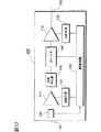
(第1の実施形態)
図1は、第1の実施形態に係る光増幅器100の概略構成図である。本実施形態に係る光増幅器100は、光入力端101から光出力端102へ順に、光カプラ130、前段光増幅部111、光フィルタ140および後段光増幅部112が直列接続されている。光増幅器100はさらに、前段光増幅部111、後段光増幅部112のそれぞれに励起光を供給する励起光源121と122、さらにこれらの励起光源121、122の光量と光フィルタ140の損失スペクトルを制御する制御回路150を備える。
【0020】
光カプラ130は、光入力端101へ入力された多重信号光の一部を分岐して制御回路150へと出力し、残部を前段光増幅部111へと出力する。前段光増幅部111は、励起光源121から励起光が供給され、光カプラ130から送られた多重信号光を一括光増幅して出力する。光フィルタ140は、この多重信号光の波長帯域において全損失が略一定であって、該波長帯域において損失の波長に対する傾きが可変である損失スペクトルを有している。後段光増幅部112は、励起光源122から励起光が供給され、光フィルタ140から送られた多重信号光を一括光増幅して、光出力端102へ出力する。
【0021】
制御回路150は、光カプラ130により分岐された多重信号光のパワーを検出する。そして、制御回路150は、その入力多重信号光パワーに基づいて、出力多重信号光のパワーが一定の目標値になるよう、励起光源121および122それぞれから出力される励起光のパワーを制御する。また、制御回路150は、その入力多重信号光パワーに基づいて、光フィルタ140の損失スペクトルを制御する。
【0022】
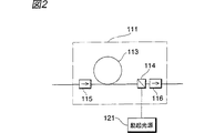
図2は、前段光増幅部111および励起光源121の説明図である。前段光増幅部111は、増幅用光ファイバ113、光カプラ114、光アイソレータ115および116を含む。光カプラ114は、励起光源121から出力された励起光を増幅用光ファイバ113へ導入するとともに、増幅用光ファイバ113から出力された信号光を通過させる。光アイソレータ115および116それぞれは、順方向へ光を通過させるが、逆方向へは光を通過させない。
【0023】
また、増幅用光ファイバ113は、励起光源121から出力された励起光により励起可能な蛍光物質が添加された光導波路である。添加される蛍光物質は、好適には希土類元素であり、より好適にはEr元素である。Er元素が添加される場合、波長1.55μm帯の信号光を光増幅することができるので好適である。また、このとき、励起光源121から出力され増幅用光ファイバ113へ供給される励起光の波長は1.48μmまたは0.98μmが好適である。後段光増幅部112および励起光源122も同様の構成である。
【0024】
次に、光フィルタ140の好適な1実施例について説明する。図3は、光フィルタ140の説明図である。この光フィルタ140は、例えば石英からなる基板10上に形成された平面光導波路回路であって、主光路20、第1の副光路21、第2の副光路22、第1の温度調整手段としてのヒータ51、および、第2の温度調整手段としてのヒータ53を備えている。
【0025】
主光路20は、基板10の一方の端面にある光入力端11に入射した光を基板10の他方の端面にある光出力端12まで導波させて出射させる光導波路であり、6つの領域A〜Fを有している。
【0026】
主光路20と第1の副光路21とは、第1の領域Aと第3の領域Cで近接して互いに光結合され、それぞれ第1の光カプラ31と第2の光カプラ32とを形成している。第2の領域Bにおいては、主光路20の光路長が第1の副光路21の光路長より長く設定され、それぞれの光路が離隔して配置されている。このようにして、主光路の第一の領域Aから第三の領域Cに至る部分と第一の副光路21とは非対称型のマッハツェンダー型干渉回路を形成している。以下、この部分を第1のマッハツェンダ干渉回路41と呼ぶ。
【0027】
同様に、主光路20と第2の副光路22とは、第4の領域Dと第6の領域Fで近接して互いに光結合され、それぞれ第3の光カプラ33と第4の光カプラ34とを形成している。第5の領域Eにおいては、主光路20の光路長が第2の副光路22の光路長より短く設定され、それぞれの光路が離隔して配置されている。このようにして、主光路の第4の領域Dから第6の領域Fに至る部分と第2の副光路22とは非対称型のマッハツェンダー型干渉回路を形成している。以下、この部分を第2のマッハツェンダ干渉回路42と呼ぶ。
【0028】
ヒータ51は、主光路20の第2の領域B上に設けられている。このヒータ51は、主光路20の温度を調整することにより、第1のマッハツェンダ干渉回路41における主光路20と第1の副光路21との光路長差を調整して、第1のマッハツェンダ干渉回路41の透過特性を調整する。また、ヒータ53は、主光路20の第5の領域E上に設けられている。このヒータ53は、主光路20の温度を調整することにより、第2のマッハツェンダ干渉回路42における主光路20と第2の副光路22との光路長差を調整して、第2のマッハツェンダ干渉回路42の透過特性を調整する。これらヒータ51および53は制御回路150により制御される。
【0029】
なお、第1の副光路21の第2の領域B上あるいは第2の副光路22の第5の領域E上にヒータを設けて、ヒータ51、ヒータ53のそれぞれの代わりとしても、両方にヒータを設置してもよい。また、ヒータに替えて冷却用のペルチエ素子を設けてもよい。
【0030】
この光フィルタ1では、光入力端11に入力し主光路20を経て光出力端12から出力される光に対する損失スペクトルL(λ)[dB]は、光カプラ31および32による主光路20と第1の副光路21との間の光結合に基づく第1のマッハツェンダ干渉回路41の透過特性T1(λ)、および、光カプラ33および34による主光路20と第2の副光路22との間の光結合に基づく第2のマッハツェンダ干渉計42の透過特性T2(λ)の双方に従う。
【0031】
一般に非対称型のマッハツェンダ干渉回路の透過特性T(λ)は、
【0032】
【数1】

【数2】
![]()
【0033】
光フィルタ1は、第1のマッハツェンダ干渉回路41および第2のマッハツェンダ干渉回路42それぞれの定数A、λ0およびΔλの各値を適切に設計することにより、所定の波長帯域中の所定波長λ1における損失L(λ1)を略一定に維持したまま、ヒータ51、53による温度調整により位相値Δφの値を変更することにより、その波長帯域における損失L(λ)および傾きS(λ)を変更することが可能である。後述するように、この光フィルタ1の傾きS(λ)は波長λに対する依存性が小さく、光フィルタ1の損失L(λ)の波長λに対する線形性が優れている。
【0034】
本発明者は各マッハツェンダ干渉計41および42それぞれの構造パラメータを代えた数種の光フィルタ1を作成し、その傾きS(λ)の可変性を確認したのでその結果について以下に説明する。
【0035】
次表は、各実施例における構造パラメータを示している。
【表1】
いずれの実施例の光フィルタにおいてもそれぞれのマッハツェンダ干渉回路41、42における光路長差は、基準温度の場合でそれぞれ12.5λ0、9.5λ0に設定した。そのうえで、ヒータ51、53を作動させて主光路20の第2の領域Bと第5の領域Eの温度をそれぞれ調整することより、マッハツェンダ干渉回路41および42それぞれの位相値Δφを符号が逆で絶対値が相等しくなるように0rad〜0.595radの範囲で変化させた。
【0037】
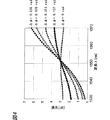
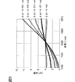
図4〜図6は、それぞれ実施例A〜Cの光フィルタの損失スペクトルを位相値Δφの各値について示したグラフである。
【0038】
実施例Aは、図4から分かるように、波長帯域1535nm〜1565nm中の中心波長1550nm付近で損失が2.73dB〜3.01dBと略一定であり、その波長帯域において傾きS(λ)を0〜5.05dB/30nmの範囲で設定可能である。また、損失2.89dB(@中心波長1550nm)の点を通る直線との偏差の最大値は、位相値Δφが0.595radであるときに±0.21dBであって充分に小さく、傾きS(λ)は線形性に優れていることが確認された。
【0039】
実施例Bは、図5から分かるように、波長帯域1535nm〜1565nm中の中心波長1550nm付近で損失が3.65dB〜3.98dBと略一定であり、その波長帯域において傾きS(λ)を0〜10dB/30nmの範囲で設定可能である。また、損失0.87dB(@中心波長1550nm)の点を通る直線との偏差の最大値は、位相値Δφの値が0.314radであるときに±0.87dBであって充分に小さく、傾きS(λ)は線形性に優れていることが確認された。
【0040】
実施例Cは、図6から分かるように、波長帯域1575nm〜1605nm中の中心波長1590nm付近で損失が2.73dB〜3.01dBと略一定であり、その波長帯域において傾きS(λ)を0〜5dB/30nmの範囲で設定可能である。また、損失2.89dB(@中心波長1590nm)の点を通る直線との偏差の最大値は、位相値Δφの値が0.595radであるときに±0.21dBであって充分に小さく、傾きS(λ)は線形性に優れていることが確認された。
【0041】
なお、主光路20の第2の領域Bと第5の領域Eのそれぞれの温度をある一定のバイアス温度に調整したときに位相値Δφの値が0になるようにマッハツェンダ干渉計41および42それぞれの構造パラメータを適切に設定すると、主光路20の第2の領域Bと第5の領域Eのそれぞれの温度を上記バイアス温度より上昇させることにより位相値Δφの値を0〜+0.595radの範囲で変化させることができ、また、主光路20の第2の領域Bと第5の領域Eのそれぞれの温度を上記バイアス温度より降下させることにより位相値Δφの値を−0.595rad〜0の範囲で変化させることができる。このようにして位相値Δφの値を−0.595rad〜+0.595radの範囲で変化させることにより、所定波長帯域において傾きS(λ)を±adB/nmの範囲で設定し得る。
【0042】
また、ヒータ51、53に替えてペルチエ素子を設けて、主光路20の第2の領域Bと第5の領域Eのそれぞれの温度を上昇または降下させることにより、位相値Δφの値を正だけでなく負にも設定することができる。このようにして位相値Δφの値を−0.595rad〜+0.595radの範囲で変化させることもできる。
【0043】
このように図3に示される光フィルタ140においては、光入力端11に入力し主光路20を経て光出力端12から出力される光に対する損失スペクトルは、光カプラ31および32による主光路20と第1の副光路21との間の光結合に基づく第1のマッハツェンダ干渉回路41の透過特性、および、光カプラ33および34による主光路20と第2の副光路22との間の光結合に基づく第2のマッハツェンダ干渉回路42の透過特性により定まる。この光フィルタ140は、基板10上に集積化されて小型である点で好適であり、また、挿入損失が小さい点でも好適である。
【0044】
次に、第1の実施形態に係る光増幅器100の動作を説明するとともに、第1の実施形態に係る光増幅器制御方法を説明する。図7A〜図7Dは、第1の実施形態に係る光増幅器100の動作を説明する図である。光フィルタ140の損失スペクトル(図7A)は、前述したように信号光の波長帯域中の所定波長λ1において損失L(λ1)が略一定であって、該波長帯域において傾きS(λ)が可変である。そして、その傾きS(λ)は、入力信号光パワーをモニタする制御回路150により制御される。
【0045】
入力信号光パワーが所定値であり、前段光増幅部111および後段光増幅部112における信号光の光増幅の利得が波長に依らず略一定である場合(図7B)、これに対して入力信号光パワーが所定値より小さくなったときには、前段光増幅部111および後段光増幅部112における信号光の光増幅の利得は、制御回路150により制御されて大きくなり、その結果、波長が長いほど利得が小さくなり、利得は波長に対して依存性を生ずる(図7C)。しかし、このときに、光フィルタ140の傾きS(λ)は制御回路150により制御されて、波長が長いほど損失が小さく設定される。したがって、前段光増幅部111および後段光増幅部112の利得の波長依存性が光フィルタ140の損失の波長依存性により相殺されて、その結果、光増幅器100全体の利得特性は、波長に依らず略一定となり、利得の平坦性が維持される(図7D)。
【0046】
以上のように、本実施形態では、入力信号光パワーが変動しても、出力信号光パワーを一定の目標値に維持するとともに、光増幅器100全体の利得平坦性を維持することができる。また、光フィルタ140の損失が信号光の波長帯域中の所定波長において略一定であるので、雑音指数が劣化することがない。なお、本実施形態において、光フィルタ140は、後段光増幅部112の後段にあってもよい。
【0047】
(第2の実施形態)
図8は、本発明に係る第2の実施形態である光増幅器200の概略構成図である。なお、この図には、光増幅器200の前段に設けられる光増幅器200Aも示されている。本実施形態に係る光増幅器200は、光入力端201から光出力端202へ順に、光カプラ230、前段光増幅部211、光フィルタ240および後段光増幅部212が直列に接続されている。光増幅器200はさらに、前段光増幅部211、後段光増幅部212のそれぞれに励起光を供給する励起光源221と222、これらの励起光源221と222と光フィルタ240の損失スペクトルを制御する制御回路250を備える。
【0048】
それぞれの構成は、図1に示される第1の実施形態と同様であるが、制御回路250の構成が相違する。制御回路250は、光カプラ230により分岐された入力信号光のパワーを検出する点では第1の実施形態と同様であるが、前段の光増幅器200Aから送信されてきた前段の光増幅器200Aの出力信号光パワーに関する情報が入力されている。そして、制御回路250は、前段の光増幅器200Aの出力信号光パワーおよび自己の入力信号光パワーに基づいて必要利得を算出し、出力信号光のパワーが一定の目標値になるよう、励起光源221および222それぞれから出力される励起光のパワーを制御する。また、制御回路250は、その必要利得に基づいて、光フィルタ240の損失スペクトルを制御する。
【0049】
具体的には、必要利得が大きくなると、前段光増幅部211および後段光増幅部212における信号光の光増幅の利得は、波長が長いほど小さくなり、利得に波長依存性が生じる。しかし、このときに、光フィルタ240の傾きS(λ)は、制御回路250により制御されて、波長が長いほど損失が小さくなるよう設定される。したがって、前段光増幅部211および後段光増幅部212の利得の波長依存性が光フィルタ240の損失スペクトルにより相殺されて、その結果、光増幅器200全体の利得特性は、波長に依らず略一定となり、利得の平坦性が維持される。
【0050】
以上のように、本実施形態でも、入力信号光パワーが変動しても、出力信号光パワーを一定の目標値に維持するとともに、光増幅器200全体の利得平坦性を維持することができる。また、光フィルタ240の損失が信号光の波長帯域中の所定波長において略一定であるので、雑音指数が劣化することがない。なお、本実施形態において、光フィルタ240は、後段光増幅部212の後段にあってもよい。
【0051】
(第3の実施形態)
図9は、本発明に係る第3の実施形態である光増幅器300の概略構成図である。本実施形態に係る光増幅器300は、光入力端301から光出力端302へ順に、光カプラ331、前段光増幅部311、後段光増幅部312、光フィルタ340および光カプラ332が直列に接続されている。光増幅器300はさらに、前段光増幅部311、後段光増幅部312のそれぞれに励起光を供給する励起光源321と322、これらの励起光源321と322と光フィルタ340の損失スペクトルを制御する制御回路350を備える。
【0052】
各構成要素の構成は、図1に示される第1の実施形態と同様であるため、説明は省略する。本実施形態では、光出力側に光カプラ332を有し、分岐した出力光の一部を制御回路350に導いている点と、光フィルタ340が多段増幅器311、312の下流に配置されている点が特徴である。
【0053】
制御回路350は、光カプラ331により分岐された入力信号光のパワーを検出するとともに、光カプラ332により分岐された出力信号光のパワーを検出する。そして、制御回路350は、出力信号光のパワーが一定の目標値になるよう、励起光源321および322それぞれから出力される励起光のパワーを制御する。また、制御回路350は、出力信号光パワーおよび入力信号光パワーに基づいて利得を算出し、その利得に基づいて、光フィルタ340の損失スペクトルを制御する。
【0054】
具体的には、利得が大きくなると、前段光増幅部311および後段光増幅部312における信号光の光増幅の利得は、波長が長いほど小さくなり、利得に波長依存性が生じる。しかし、このときに、光フィルタ340の傾きS(λ)は、制御回路350により制御されて、波長が長いほど損失が小さくなるよう設定される。したがって、前段光増幅部311および後段光増幅部312の利得の波長依存性が光フィルタ340の損失スペクトルにより相殺されて、その結果、光増幅器300全体の利得特性は、波長に依らず略一定となり、利得の平坦性が維持される。
【0055】
以上のように、本実施形態でも、入力信号光パワーが変動しても、出力信号光パワーを一定の目標値に維持するとともに、光増幅器300全体の利得平坦性を維持することができる。また、光フィルタ340の損失が信号光の波長帯域中の所定波長において略一定であるので、雑音指数が劣化することがない。なお、本実施形態において、光フィルタ340は、前段光増幅部311と後段光増幅部312との間にあってもよい。
【0056】
(第4の実施形態)
図10Aは、本発明に係る第4の実施形態である光増幅器400の概略構成図である。実施形態に係る光増幅器400は、光入力端401から光出力端402へ順に、前段光増幅部411、後段光増幅部412および光フィルタ440が直列に接続されている。光増幅器400はさらに、前段光増幅部411、後段光増幅部412のそれぞれに励起光を供給する励起光源421と422、光出力端402から出力される各波長の信号光のパワーをモニタするスペクトルモニタデバイス460、励起光源421と422の励起光出力と光フィルタ440の損失スペクトルを制御する制御回路450を備える。
【0057】
本実施形態ではスペクトルモニタデバイス460を有している点が特徴である。その他の構成は他の実施形態と同様であるためその説明を省略する。
【0058】
このスペクトルモニタデバイス460は、光出力端402から出力される光の一部が分岐されて導かれるか、図3に示した構造を有する光フィルタ440の第2の副光路22から出力される光が導かれ、導かれた光を分波する。このスペクトルモニタデバイス460は、例えばアレイ導波路回折格子(AWG: Arrayed-Waveguide Grating)により実現することができ、この場合には、図3に示した構造を有する光フィルタ440とともに共通の基板上に形成することができるので装置全体の小型化が可能である。
【0059】
制御回路450は、スペクトルモニタデバイス460により分波された各波長の出力信号光のパワーを検出する。そして、制御回路450は、出力信号光のパワーが一定の目標値になるよう、励起光源421および422それぞれから出力される励起光のパワーを制御する。また、制御回路450は、各波長の出力信号光パワーの偏差に基づいて、その偏差が小さくなるように光フィルタ440の損失スペクトルを制御する。
【0060】
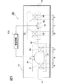
ここで、光フィルタ440およびスペクトルモニタデバイス460の好適な1実施例について説明する。図11は、光フィルタ440およびスペクトルモニタデバイス460の説明図である。光フィルタ440およびスペクトルモニタデバイス460は共通の基板10A上に形成されている。光フィルタ440は、図3に示した構成と同様の構成である。スペクトルモニタデバイス460は、基板10A上に形成されたAWGである。すなわち、スペクトルモニタデバイス460は、入力側スラブ導波路61、複数のチャネル導波路を有するアレイ導波路部62、出力側スラブ導波路63および出力側チャネル導波路641〜64Nを備える。
【0061】
入力側スラブ導波路61には、光フィルタ440の第2の副光路22から出力される光が入力され、その光をアレイ導波路部62の各チャネル導波路それぞれへと分波して出力する。アレイ導波路部62の複数のチャネル導波路それぞれは、入力側スラブ導波路61から出力側スラブ導波路63までの光路長が互いに異なり、導波する光に対して互いに異なる位相を与える。出力側スラブ導波路63は、アレイ導波路部62の複数のチャネル導波路それぞれから光を入力して、出力側チャネル導波路641〜64Nそれぞれへ出力する。
【0062】
出力側チャネル導波路641〜64Nそれぞれへ出力される光は、光フィルタ440の第2の副光路22から出力された光が分波された各波長の信号光である。そこで、制御回路450は、スペクトルモニタデバイス460の出力側チャネル導波路641〜64Nそれぞれへ出力された各波長の信号光のパワーを検出して、この各波長の信号光パワーの偏差が小さくなるように、光フィルタ440の損失傾斜を制御する。なお、制御回路450は、スペクトルモニタデバイス460により分波された各波長の信号光のうちの2波長(例えば最大波長および最小波長)の信号光のパワーの偏差が小さくなるように、光フィルタ440の損失傾斜を制御してもよい。
【0063】
図10Bは、この第4の実施形態の変形形態であり、光入力端401側に入力信号光中の監視光成分を分岐する光カプラ430を備えている点が図10Aに示される第4の実施形態と相違する。監視光には、例えば、送られてくる多重信号光中の最短波長と最長波長に関する情報が含まれており、制御回路450はこれらの情報を読み出して、パワー偏差を求める2つの波長を決定する。
【0064】
以上のように、本実施形態でも、入力信号光パワーが変動しても、出力信号光パワーを一定の目標値に維持するとともに、光増幅器400全体の利得平坦性を維持することができる。また、光フィルタ440の損失が信号光の波長帯域中の所定波長において略一定であるので、雑音指数が劣化することがない。更に、特に本実施形態では、光フィルタ440の損失傾斜がフィードバック制御されるので、安定した動作が可能である。
【0065】
(第5の実施形態)
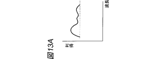
図12は、本発明に係る第5の実施形態である光増幅器500の概略構成図である。本実施形態に係る光増幅器500は、第1の実施形態に係る光増幅器100において前段光増幅部111と光フィルタ140との間に利得等化器170を挿入したものである。利得等化器170は、前段光増幅部111および後段光増幅部112の固有の利得波長依存性を等化するものである。この利得等化器170は、例えば、光ファイバのコアに屈折率変調が形成された光ファイバグレーティング素子や、ファブリペロー共振器構造を有するエタロン型フィルタ等により実現することができる。
【0066】
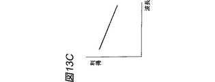
次に、第5の実施形態に係る光増幅器500の動作、すなわち、第5の実施形態に係る光増幅方法を説明する。図13A〜図13Cは、第5の実施形態に係る光増幅器500の動作を説明する図である。入力信号光パワーが所定値であるときであっても、前段光増幅部111および後段光増幅部112の利得スペクトルは、厳密には一定とはならずに、前段光増幅部111および後段光増幅部112に固有の利得波長依存性を有している(図13A)。利得等化器170は、このときの前段光増幅部111および後段光増幅部112の利得スペクトルの形状と同様の形状の損失スペクトルを有している。したがって、出力される光のスペクトルは平坦なものとなる。
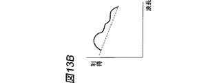
【0067】
これに対して入力信号光パワーが所定値より小さくなったときには、前段光増幅部111および後段光増幅部112における信号光の光増幅の利得は、制御回路150により制御されて大きくなり、その結果、波長が長いほど利得が小さくなり利得の波長依存性が変化する(図13B)。しかし、このときに、光フィルタ140の損失スペクトルは制御回路150により制御されて、波長が長いほど損失が小さくなるよう設定される。
【0068】
前段光増幅部111および後段光増幅部112から出力された光は、その固有の利得波長依存性が利得等化器170により等化され、図13Cに示されるように利得(dB)が波長に対して線型に変化するよう調整される。その後、残存する利得の波長依存性は、光フィルタ140の損失スペクトルにより相殺される。その結果、光増幅器500全体の利得特性は、波長に依らず略一定となり、その平坦性が維持される。
【0069】
以上のように、本実施形態でも、入力信号光パワーが変動しても、出力信号光パワーを一定の目標値に維持するとともに、光増幅器500全体の利得平坦性を維持することができる。特に本実施形態では、光フィルタ140に加えて利得等化器170を設けたことにより、光増幅器500全体の利得平坦性は優れたものとなる。また、光フィルタ140の損失が信号光の波長帯域中の所定波長において略一定であるので、雑音指数が劣化することがない。なお、本実施形態において、光フィルタ140および利得等化器170の双方または何れか一方は、後段光増幅部112の後段にあってもよい。もちろん、第2〜第4の実施形態に係る光増幅器の何れに利得等化器を挿入しても同様の効果が得られる。
【0070】
(第6の実施形態)
図14Aは、本発明に係る第6の実施形態である光増幅器300aの概略構成図である。本実施形態に係る光増幅器300aは、図9に示される第3の実施形態の光増幅器300の最終段の光カプラ332に代えてASE光レベル検出器333を設置している点のみが相違する。
【0071】
このASE光レベル検出器333は、光フィルタ340から出力された信号光の所定波長帯域の両端外側に位置するそれぞれの波長の自然放出光(ASE光)レベルを検出するものであり、制御回路350は、検出した長波長側と短波長側のASE光レベル差を一定に維持するように光フィルタ340の損失スペクトルを調整する。ASE光のレベル差を利用して制御することで制御が容易になるという利点がある。
【0072】
多重信号光とともに多重信号光中の最短波長と最長波長に関する情報を有する監視光が送られてくる場合には、光カプラ331で分岐された監視光を制御回路350で受信してこれらの情報を読み出し、ASE光レベル検出器333でASE光レベルを検出する波長を読み出した最短波長と最長波長の外側近傍の波長となるよう設定すると、多重信号光中の最短波長と最長波長が一定でない場合にも安定した光増幅を行える。
【0073】
図14Bは、本発明に係る第6の実施形態の変形形態である光増幅器600の概略構成図である。具体的な構成は、光入力端601から光出力端602へ順に、光カプラ630、前段光増幅部611、後段光増幅部612、光カプラ631および光フィルタ640が直列接続されて構成されている。光増幅器600はさらに、前段、後段の各光増幅部611、612のそれぞれに励起光を供給する励起光源621、622、さらにこれらの励起光源621、622の光量と光フィルタ640の損失スペクトルを制御する制御回路650を備える。また、光カプラ631で分岐された光はスペクトルモニタデバイス660と可変バンドパスフィルタ670に導かれる。可変バンドパスフィルタ670を透過した光は受光素子680によって検出される。スペクトルモニタデバイス660と受光素子680の出力は制御回路650へと送られる。各増幅部611、612と光フィルタ640の構成は第1の実施形態と同一であるため説明を省略する。
【0074】
本実施形態では、スペクトルモニタデバイス660で信号光中の最短波長の光と最長波長の光のそれぞれの波長を検出する。そして、可変バンドパスフィルタ670を制御することで出力多重信号光に含まれるこれらの波長の外側、すなわち、検出された最短波長より短波長側と検出された最長波長より長波長側のそれぞれのASE光レベルを受光素子680により検出する。そして、制御回路650は、検出した長波長側と短波長側のASE光レベル差を一定に維持するように光フィルタ640の損失スペクトルを調整する。この場合も制御が容易になるという利点がある。
【0075】
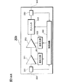
(第7の実施形態)
図15は、本発明に係る第7の実施形態である光増幅器700の概略構成図である。この光増幅器700は、分散補償ファイバ(DCF: Dispersion Compensating Fiber)770を内蔵している。
【0076】
具体的な構成は、光入力端701から光出力端702へ順に、光カプラ730、前段光増幅部711、光フィルタ740、中段光増幅部712、利得等化器760、DCF770および後段光増幅部713が直列接続されて構成されている。光増幅器700はさらに、前段、中段、後段の各光増幅部711〜713のそれぞれに励起光を供給する励起光源721〜723、さらにこれらの励起光源721〜723の光量と光フィルタ740の損失スペクトルを制御する制御回路750を備える。各増幅部711〜713と光フィルタ740の構成は第1の実施形態と同一であるため説明を省略する。
【0077】
本発明者は損失スペクトルを調整可能な光フィルタを用いた本実施形態の光増幅器700の雑音特性改善効果を確認するため、従来一般的であった全損失率のみを調整する可変光減衰器を光フィルタとして搭載した場合との比較実験を行った。
【0078】
実験では、−28dbm/ch〜−12dbm/chの16dBのダイナミックレンジの入力レベルに対する雑音特性を測定した。可変光減衰器を用いる場合、一般的に16dBもの入力ダイナミックレンジへの対応は困難であるため、−28dbm/ch〜−20dbm/chと−20dbm/ch〜−12dbm/chの2種に分けてこれらを組み合わせて使用した場合も合わせて測定した。
【0079】
測定結果を図16に示す。ここで、○が可変光減衰器を用いて全レンジを1種の光増幅器で増幅した場合、△が可変光減衰器を用いて全レンジを分割して2種の光増幅器でそれぞれ増幅した場合、□が本発明に係る第7の実施形態の光増幅器で増幅した場合の入力レベルに対する雑音特性を示している。
【0080】
本発明に係る光増幅器では、全ての入力レベルにおいて雑音特性が改善され、さらに適応できるダイナミックレンジが拡大できる効果のあることが確認された。
【0081】
次に、光フィルタの変形例について説明する。図4〜図6に示される損失スペクトルを有する光フィルタは、使用波長帯域の中心波長付近で損失が略一定であったが、損失が略一定となる波長λ1が短波長側あるいは長波長側にずれていてもよい。図17に損失スペクトルを示す光フィルタは、この波長λ1が波長帯域の最短波長に位置している。そして、損失スペクトルはL0(λ) とL2(λ)の間で可変でき、光フィルタへ入力される光のパワーが最大のときには、損失スペクトルがL2(λ)となるよう調整し、入力される光のパワーが最小のときには、損失が波長によらずに一定となるL0(λ)となるよう調整する。その中間のときにはL1(λ)となるよう調整する。このようにすることで、特に短波長帯域での雑音指数劣化を抑制できる。また、入力されるパワーが最小のときには、透過率が最大となるので、特に入力光のパワーが小さいときの雑音特性回前効果がある。
【0082】
(第8の実施形態)
図18は、本発明に係る第8の実施形態である光増幅器300bの概略構成図である。本実施形態に係る光増幅器300bは、図9に示される第3の実施形態の光増幅器300の最終段の光カプラ332からの分岐先に出力多重信号光中に含まれる信号光の数(波数)を検出する波数モニタ335が配置されている点が相違する。
【0083】
入力多重信号光中に含まれる波数が変動すると、個々の信号光のパワーは変動せずとも入力多重信号光のパワーは変動する。そのため、単に増幅後の出力多重信号光のパワーを一定に維持しようとすると、波数が減少した場合には個々の信号光のパワーが増大し、波数が増加した場合には個々の信号光のパワーは減少して変動することになる。
【0084】
本実施形態では、制御回路350bが波数モニタ335の出力をもとにして波数に比例して出力多重信号光のパワーの目標値を調整する。これにより、波数が変動した場合も個々の信号光の増幅後の光パワーを一定に維持することができる。
【0085】
本発明は、上記実施形態に限定されるものではなく種々の変形が可能である。例えば、増幅用光ファイバに添加される蛍光物質は、Er元素に限られるものではなく、他の希土類元素(例えば、Tm元素、Pr元素、Nd元素等)であってもよい。増幅用光ファイバに替えて、励起光により励起可能な蛍光物質が添加された平面光導波路であってもよい。必ずしも前段光増幅部と後段光増幅部とに区分されていなくてもよく、あるいは3個以上の光増幅部を有していてもよい。
【0086】
【産業上の利用可能性】
本発明に係る光増幅器、光増幅方法は特に、多重信号光を伝送する波長多重伝送システムにおいて好適に使用される。
【0087】
【図面の簡単な説明】
【図1】 本発明に係る光増幅器の第1の実施形態の概略構成図である。
【図2】 第1の実施形態の前段光増幅部および励起光源の説明図である。
【図3】 第1の実施形態の光フィルタの説明図である。
【図4】 光フィルタの実施例Aにおいて位相値Δφを変更したときの損失スペクトルを示したグラフである。
【図5】 光フィルタの実施例Bにおいて位相値Δφを変更したときの損失スペクトルを示したグラフである。
【図6】 光フィルタの実施例Cにおいて位相値Δφを変更したときの損失スペクトルを示したグラフである。
【図7】 第1の実施形態の光増幅器の動作を説明する図である。
【図8】 本発明に係る光増幅器の第2の実施形態の概略構成図である。
【図9】 本発明に係る光増幅器の第3の実施形態の概略構成図である。
【図10】 本発明に係る光増幅器の第4の実施形態と、その変形形態の概略構成図である。
【図11】 第3の実施形態における光フィルタおよびスペクトルモニタデバイスの説明図である。
【図12】 本発明に係る光増幅器の第5の実施形態の概略構成図である。
【図13】 本発明に係る光増幅器の第5の実施形態の動作を説明する図である。
【図14】 本発明に係る光増幅器の第6の実施形態とその変形形態の概略構成図であり、
【図15】 本発明に係る光増幅器の第7の実施形態の概略構成図である。
【図16】 上記第7の実施形態と従来の光増幅器の雑音特性を比較したグラフである。
【図17】 本発明に係る光増幅器に用いられる光フィルタの変形例の損失スペクトルを説明する図である。
【図18】 本発明に係る光増幅器の第8の実施形態の概略構成図である。
【符号の説明】
10…基板、11、101、201、301、401、601、701…光入力端、12、102、202、302、402、602、702…光出力端、20…主光路、21、22…副光路、31〜34、114、130、230、331、332、430、630、631、730…光カプラ、41、42…マッハツェンダ干渉回路(干渉計)、51、53…ヒータ、61…入力側スラブ導波路、62…アレイ導波路部、63…出力側スラブ導波路、100、200、300、400、500、600、700…光増幅器、111、211、311、411、611、711…前段光増幅部、112、212、312、412、612、713…後段光増幅部、113…増幅用光ファイバ、115…光アイソレータ、121、122、221、321、421、621…励起光源、140、240、340、440、640、740…光フィルタ、150、250、350、450、650、750…制御回路、170、760…利得等化器、310…多段増幅器、333…光レベル検出器、335…波数モニタ、460、660…スペクトルモニタデバイス、670…可変バンドパスフィルタ、680…受光素子、712…中段光増幅部。 [0001]
BACKGROUND OF THE INVENTION
The present invention relates to an optical amplifier and an optical amplification method for collectively amplifying multiplexed signal light obtained by combining a plurality of signal lights having different wavelengths belonging to a predetermined wavelength band.
[0002]
[Prior art]
As an optical amplifier, there is known an optical amplifier that amplifies signal light by guiding signal light and excitation light of the fluorescent material to a waveguide to which the fluorescent material is added. Such an optical amplifier is provided in a relay station or the like in the optical transmission system. In particular, an optical amplifier used in a wavelength division multiplexing transmission system that transmits a multiplexed signal light that is a combination of a plurality of signal lights of different wavelengths, amplifies each of the plurality of signal lights together with an equal gain, It is necessary to amplify and output the power of each light to a certain target value.
[0003]
For example,
[0004]
[Problems to be solved by the invention]
However, in the technique described in the above-mentioned
[0005]
In the technique described in the above-mentioned
[0006]
The present invention has been made to solve the above problems, and can maintain the output signal light power and gain flatness without degrading the noise figure even when the input signal light power fluctuates. And it aims at providing the optical amplification method.
[0007]
[Means for Solving the Problems]
In order to achieve the above object, an optical amplifier according to the present invention is an optical amplifier that collectively amplifies multiplexed signal light that is a combination of a plurality of signal lights belonging to a predetermined wavelength band and having different wavelengths. ) Having an optical waveguide to which a fluorescent material is added, and one or a plurality of optical amplification units that amplify the multiplexed signal light using the optical excitation of the fluorescent material; and (2) a predetermined excitation light is applied to the optical amplification unit. An excitation light source to supply, (3)According to the change in wavelength dependence of gain in the optical amplification unit,An optical filter capable of changing the slope dL / dλ of the loss L (dB) with respect to the wavelength λ (nm) within a predetermined wavelength band; and (4) excitation of the excitation light source so that the optical power after amplification becomes a predetermined target value. While controlling the light output,The slope dL / dλ of the optical filter is set so as to flatten the wavelength dependence of the final gain.And (5) a gain equalizer that compensates for the wavelength dependence of the gain unique to the optical amplifying unit.
[0008]
On the other hand, the optical amplification method according to the present invention includes (1) a step of conducting optical amplification by guiding the multiplexed signal light to an optical waveguide to which a fluorescent material is added together with predetermined excitation light, and (2) at least before or after amplification. One of the multiple signal lightsIn response to a change in wavelength dependence of gain in the optical amplification unitIn a predetermined wavelength band, the slope dL / dλ of the loss L (dB) with respect to the wavelength λ (nm) is guided to a changeable optical filter, and the gain d in the optical amplification process is adjusted by adjusting the slope dL / dλ of the optical filter. A step of reducing the wavelength dependence; and (3) a step of adjusting the intensity of the pumping light to adjust the optical power after amplification to a predetermined target value.(4) adjusting the slope dL / dλ of the optical filter so as to flatten the wavelength dependence of the final gain; (5)And a step of reducing the wavelength dependence of the inherent gain in the optical amplification step by a predetermined gain equalizer.
[0009]
According to the optical amplifier or the optical amplification method of the present invention, the output signal light power from the optical amplifier can be maintained at a predetermined target value even if the input signal light power to the optical amplifier varies. Even if the wavelength dependence of the gain of the optical amplification unit may occur due to fluctuations in the input signal light power, the gain of the entire optical amplifier can be adjusted by adjusting the slope dL / dλ of the loss L of the optical filter with respect to the wavelength λ. Flatness can be maintained.In addition, the gain equalizer equalizes the wavelength dependence of the gain inherent to the optical amplifier, and the optical filter compensates for the power fluctuation of the input signal light, so that the gain flatness of the entire optical amplifier is improved. Control and adjustment become easy.
[0010]
This light filterThe characteristics ofWithin a specified wavelength band
L≈a (λ−λc) + b
(Λc (nm) and b (dB) are constants)Shi, A (dB / nm)If is variable,The inclination dL / dλ can be easily adjusted. When this λc is set within this predetermined wavelength band, the loss L at the wavelength λc within the predetermined wavelength band is always constant, and a design with an emphasis on noise characteristics at λc becomes possible.
[0011]
It is preferable that a wave number monitor for detecting the number of signal lights included in the multiplexed signal light is further provided, and the control means adjusts the target value of the amplified optical power according to the number of signal lights detected by the wave number monitor. By increasing or decreasing the number of signal lights, the power of each signal light can be kept constant even if the power of the input signal light varies.
[0012]
The adjustment of the slope dL / dλ of the optical filter may be performed based on, for example, 1) the detection result of the input optical power detection means for detecting the optical power input to the optical amplification unit, and 2) the gain of the optical amplification unit May be performed based on the detection result of the gain detection means for detecting 3) the light output from the optical amplifierInIt may be performed based on the detected power deviation of the shortest and longest wavelengths by detecting each wavelength and output of the included signal light, or 4) a predetermined wavelength band of light output from the optical amplifying unit You may carry out so that the level difference of each ASE light level detected by the ASE light level detection means which detects each ASE light level in the both ends outer side may become fixed. Detects the wavelength and output of the signal light included in the light output from the optical amplifier, and detects the ASE light levels on the short wavelength side and the longest wavelength side of the detected shortest wavelength light. And may be used for adjustment. In the case of 3) and 4), the wavelength for detecting the power deviation and the ASE light level may be determined based on information on the shortest and longest wavelengths transmitted together with the multiplexed signal light.
[0013]
Furthermore, it is preferable to adjust the loss L so as to be substantially constant regardless of the wavelength when the total transmittance of the optical filter in the predetermined wavelength band is adjusted to the maximum. In this way, it is possible to reduce the noise figure especially when the power of the input multiplexed signal light is small.
[0014]
Any of these configurations and methods makes it easy to adjust the inclination dL / dλ of the optical filter, and the object of the present invention can be realized.
[0015]
The optical filter in the optical amplifier according to the present invention includes (1) a main optical path that guides multiplexed signal light and is divided into first to sixth regions in order from the upstream side, and (2) a first of the main optical paths. And the third region is arranged so close that the propagating light is optically coupled, and is separated from the second region of the main optical path so that the propagating light is not optically coupled. The first sub optical path having a length corresponding to the first optical path is different from the main optical path, and (3) the fourth and sixth areas of the main optical path are close to the extent that the propagating light is optically coupled. A second sub optical path that is spaced apart from the fifth region of the optical path so that the propagating light is not optically coupled, and whose length corresponding to the fifth region of the main optical path is different from the main optical path; (4) The first temperature adjustment arranged in at least one of the second region of the main optical path and the region corresponding to the second region of the main optical path of the first sub optical path And (5) a second temperature regulator disposed in at least one of the fifth region of the main optical path and the fifth region of the main optical path of the second sub optical path. Is preferred.
[0016]
On the other hand, in the optical amplification method according to the present invention, (1) a main optical path that guides multiplexed signal light and is divided into first to sixth regions in order from the upstream side, and (2) a first of the main optical paths. And the third region is arranged so close that the propagating light is optically coupled, and is separated from the second region of the main optical path so that the propagating light is not optically coupled. The first sub optical path having a length corresponding to the first optical path is different from the main optical path, and (3) the fourth and sixth areas of the main optical path are close to the extent that the propagating light is optically coupled. A second sub optical path that is spaced apart from the fifth region of the optical path so that the propagating light is not optically coupled, and whose length corresponding to the fifth region of the main optical path is different from the main optical path; The step of reducing the wavelength dependence of gain using an optical filter comprising: at least one of the first sub optical path and the main optical path corresponding to the first sub optical path and the first optical path; It is preferable that by adjusting the temperature of at least one of a region corresponding to the sub-path and the main path for adjusting the inclination dL / d [lambda] of the optical filter.
[0017]
The first and second sub optical paths and the corresponding main optical paths respectively form Mach-Zehnder type interference devices. By adjusting the temperature of at least one optical path in each Mach-Zehnder type interference device, it becomes possible to adjust the wavelength dependence of the loss in each main optical path, and as an optical filter in the optical amplifier and optical amplification method according to the present invention Is preferred.
[0018]
DETAILED DESCRIPTION OF THE INVENTION
DESCRIPTION OF EXEMPLARY EMBODIMENTS Hereinafter, preferred embodiments of the invention will be described in detail with reference to the accompanying drawings. In order to facilitate the understanding of the description, the same reference numerals are given to the same components in the drawings as much as possible, and duplicate descriptions are omitted.
[0019]
(First embodiment)
FIG. 1 is a schematic configuration diagram of an
[0020]
The
[0021]
The
[0022]
FIG. 2 is an explanatory diagram of the pre-stage
[0023]
The amplification
[0024]
Next, a preferred embodiment of the
[0025]
The main
[0026]
The main
[0027]
Similarly, the main
[0028]
The
[0029]
It should be noted that a heater is provided on the second region B of the first sub
[0030]
In this
[0031]
Generally, the transmission characteristic T (λ) of an asymmetric Mach-Zehnder interference circuit is
[0032]
[Expression 1]
[Expression 2]
![]()
[0033]
The
[0034]
The present inventor created several types of
[0035]
The following table shows the structural parameters in each example.
[Table 1]
The optical path length difference in each Mach-
[0037]
4 to 6 are graphs showing the loss spectra of the optical filters of Examples A to C for each value of the phase value Δφ, respectively.
[0038]
In Example A, as can be seen from FIG. 4, the loss is approximately constant at 2.73 dB to 3.01 dB in the vicinity of the
[0039]
As can be seen from FIG. 5, in Example B, the loss is approximately constant from 3.65 dB to 3.98 dB in the vicinity of the
[0040]
As can be seen from FIG. 6, in Example C, the loss is approximately constant at 2.73 dB to 3.01 dB in the vicinity of the
[0041]
It should be noted that the Mach-
[0042]
Further, a Peltier element is provided in place of the
[0043]
As described above, in the
[0044]
Next, the operation of the
[0045]
When the input signal light power is a predetermined value and the optical amplification gain of the signal light in the upstream
[0046]
As described above, in this embodiment, even when the input signal light power varies, the output signal light power can be maintained at a constant target value, and the gain flatness of the entire
[0047]
(Second Embodiment)
FIG. 8 is a schematic configuration diagram of an
[0048]
Each configuration is the same as that of the first embodiment shown in FIG. 1, but the configuration of the
[0049]
Specifically, when the required gain increases, the gain of signal light optical amplification in the front-stage
[0050]
As described above, also in this embodiment, even when the input signal light power fluctuates, the output signal light power can be maintained at a constant target value, and the gain flatness of the entire
[0051]
(Third embodiment)
FIG. 9 is a schematic configuration diagram of an
[0052]
The configuration of each component is the same as that of the first embodiment shown in FIG. In this embodiment, an
[0053]
The
[0054]
Specifically, as the gain increases, the optical amplification gain of the signal light in the front-stage
[0055]
As described above, also in this embodiment, even when the input signal light power varies, the output signal light power can be maintained at a constant target value, and the gain flatness of the entire
[0056]
(Fourth embodiment)
FIG. 10A is a schematic configuration diagram of an
[0057]
This embodiment is characterized by having a
[0058]
The
[0059]
The
[0060]
A preferred embodiment of the
[0061]
The input
[0062]
Output
[0063]
FIG. 10B is a modification of the fourth embodiment. The fourth embodiment shown in FIG. 10A includes an
[0064]
As described above, also in this embodiment, even if the input signal light power varies, the output signal light power can be maintained at a constant target value, and the gain flatness of the entire
[0065]
(Fifth embodiment)
FIG. 12 is a schematic configuration diagram of an
[0066]
Next, the operation of the
[0067]
On the other hand, when the input signal light power becomes smaller than a predetermined value, the gain of the signal light optical amplification in the front-stage
[0068]
The light output from the pre-stage
[0069]
As described above, also in this embodiment, even when the input signal light power varies, the output signal light power can be maintained at a constant target value, and the gain flatness of the entire
[0070]
(Sixth embodiment)
FIG. 14A is a schematic configuration diagram of an
[0071]
The ASE
[0072]
When the monitoring light having the information on the shortest wavelength and the longest wavelength in the multiplexed signal light is sent together with the multiplexed signal light, the monitoring light branched by the
[0073]
FIG. 14B is a schematic configuration diagram of an
[0074]
In the present embodiment, the
[0075]
(Seventh embodiment)
FIG. 15 is a schematic configuration diagram of an
[0076]
Specifically, in order from the
[0077]
In order to confirm the effect of improving the noise characteristics of the
[0078]
In the experiment, noise characteristics were measured with respect to an input level of a dynamic range of 16 dB from −28 dbm / ch to −12 dbm / ch. When using a variable optical attenuator, it is generally difficult to cope with an input dynamic range of 16 dB. Measurements were also made when these were used in combination.
[0079]
The measurement results are shown in FIG. Here, when ○ is amplified using a variable optical attenuator and the entire range is amplified with one type of optical amplifier, Δ is divided using the variable optical attenuator and the entire range is divided and amplified with two types of optical amplifiers. , □ indicate noise characteristics with respect to the input level when amplified by the optical amplifier according to the seventh embodiment of the present invention.
[0080]
In the optical amplifier according to the present invention, it was confirmed that the noise characteristics were improved at all input levels, and that the adaptable dynamic range could be expanded.
[0081]
Next, a modified example of the optical filter will be described. The optical filter having the loss spectrum shown in FIGS. 4 to 6 has a substantially constant loss near the center wavelength of the used wavelength band, but the wavelength λ at which the loss is substantially constant.1May be shifted to the short wavelength side or the long wavelength side. The optical filter whose loss spectrum is shown in FIG.1Is located at the shortest wavelength of the wavelength band. And the loss spectrum is L0(λ) and L2When the power of light input to the optical filter is maximum, the loss spectrum is L2L is adjusted so as to be (λ), and the loss is constant regardless of the wavelength when the input light power is minimum.0Adjust to (λ). L in the middle1Adjust to (λ). By doing so, it is possible to suppress noise figure deterioration particularly in a short wavelength band. Further, since the transmittance is maximized when the input power is minimum, there is a noise characteristic recirculation effect particularly when the input light power is small.
[0082]
(Eighth embodiment)
FIG. 18 is a schematic configuration diagram of an
[0083]
When the wave number included in the input multiplexed signal light fluctuates, the power of the input multiplexed signal light fluctuates even though the power of each signal light does not fluctuate. Therefore, simply trying to maintain the power of the amplified output multiplexed signal light constant, the power of the individual signal light increases when the wave number decreases, and the power of the individual signal light when the wave number increases. Will decrease and fluctuate.
[0084]
In the present embodiment, the
[0085]
The present invention is not limited to the above embodiment, and various modifications can be made. For example, the fluorescent material added to the amplification optical fiber is not limited to the Er element, but may be other rare earth elements (eg, Tm element, Pr element, Nd element, etc.). Instead of the amplification optical fiber, a planar optical waveguide to which a fluorescent substance that can be excited by excitation light is added may be used. It does not necessarily have to be divided into the front-stage optical amplification section and the rear-stage optical amplification section, or may have three or more optical amplification sections.
[0086]
[Industrial applicability]
The optical amplifier and the optical amplification method according to the present invention are particularly preferably used in a wavelength division multiplexing transmission system that transmits multiplexed signal light.
[0087]
[Brief description of the drawings]
FIG. 1 is a schematic configuration diagram of a first embodiment of an optical amplifier according to the present invention.
FIG. 2 is an explanatory diagram of a pre-stage optical amplification unit and a pumping light source according to the first embodiment.
FIG. 3 is an explanatory diagram of an optical filter according to the first embodiment.
4 is a graph showing a loss spectrum when the phase value Δφ is changed in Example A of the optical filter. FIG.
FIG. 5 is a graph showing a loss spectrum when the phase value Δφ is changed in Example B of the optical filter.
6 is a graph showing a loss spectrum when the phase value Δφ is changed in Example C of the optical filter. FIG.
FIG. 7 is a diagram illustrating the operation of the optical amplifier according to the first embodiment.
FIG. 8 is a schematic configuration diagram of a second embodiment of an optical amplifier according to the present invention.
FIG. 9 is a schematic configuration diagram of a third embodiment of an optical amplifier according to the present invention.
FIG. 10 is a schematic configuration diagram of a fourth embodiment of an optical amplifier according to the present invention and a modification thereof.
FIG. 11 is an explanatory diagram of an optical filter and a spectrum monitor device according to a third embodiment.
FIG. 12 is a schematic configuration diagram of a fifth embodiment of an optical amplifier according to the present invention.
FIG. 13 is a diagram for explaining the operation of the fifth embodiment of the optical amplifier according to the present invention;
FIG. 14 is a schematic configuration diagram of a sixth embodiment of an optical amplifier according to the present invention and a modification thereof;
FIG. 15 is a schematic configuration diagram of a seventh embodiment of an optical amplifier according to the present invention.
FIG. 16 is a graph comparing the noise characteristics of the seventh embodiment and a conventional optical amplifier.
FIG. 17 is a diagram illustrating a loss spectrum of a modification of the optical filter used in the optical amplifier according to the present invention.
FIG. 18 is a schematic configuration diagram of an eighth embodiment of an optical amplifier according to the present invention.
[Explanation of symbols]
DESCRIPTION OF
Claims (21)
前記多重信号光を導波させ、上流側から順に第1〜第6の領域に区分される主光路と、
前記主光路の第1及び第3の領域に対しては伝搬光が光結合する程度に近接し、前記主光路の第2の領域に対しては伝搬光が光結合しない程度に離隔されて配置され、前記主光路の第2の領域に対応する領域の長さが前記主光路と異なる第1の副光路と、
前記主光路の第4及び第6の領域に対しては伝搬光が光結合する程度に近接し、前記主光路の第5の領域に対しては伝搬光が光結合しない程度に離隔されて配置され、前記主光路の第5の領域に対応する領域の長さが前記主光路と異なる第2の副光路と、
前記主光路の第2の領域及び前記第1の副光路の前記主光路の第2の領域に対応する領域の少なくとも一方に配置されている第一の温度調整器と、
前記主光路の第5の領域及び前記第2の副光路の前記主光路の第5の領域に対応する領域の少なくとも一方に配置されている第二の温度調整器とを備えている請求項1記載の光増幅器。The optical filter is
A main optical path that guides the multiplexed signal light and is divided into first to sixth regions in order from the upstream side;
The first and third regions of the main optical path are close enough to propagate light, and are separated from the second region of the main optical path so as not to propagate light. A first sub optical path in which the length of the area corresponding to the second area of the main optical path is different from the main optical path;
The fourth and sixth regions of the main optical path are close enough to propagate light and optically coupled to the fifth region of the main optical path so that the propagated light is not optically coupled. A second sub optical path in which the length of the area corresponding to the fifth area of the main optical path is different from the main optical path;
A first temperature controller disposed in at least one of the second region of the main optical path and the region corresponding to the second region of the main optical path of the first sub optical path;
2. A second temperature controller disposed in at least one of a fifth region of the main optical path and a region corresponding to the fifth region of the main optical path of the second sub optical path. The optical amplifier described.
前記多重信号光を所定の励起光とともに蛍光物質が添加された光導波路に導いて光増幅する工程と、
増幅前あるいは増幅後の少なくともいずれか一方の前記多重信号光を、前記光増幅部における利得の波長依存性の変化に応じて前記所定の波長帯域内において損失L(dB)の波長λ(nm)に対する傾きdL/dλを変更可能な光フィルタに導き、前記光フィルタの傾きdL/dλを調整することにより、前記光増幅工程における利得の波長依存性を低減する工程と、
前記励起光の強度を調整して増幅後の光パワーを所定の目標値になるように調整する工程と、
最終的な利得の波長依存性を平坦化させるように、前記光フィルタの傾きdL/dλを調整する工程と、
所定の利得等化器により前記光増幅工程における固有の利得の波長依存性を低減する工程と、
を備えている光増幅方法。An optical amplification method that collectively amplifies multiple signal lights that belong to a predetermined wavelength band and combine a plurality of signal lights having different wavelengths,
Guiding the multiplexed signal light to an optical waveguide to which a fluorescent material is added together with predetermined excitation light, and amplifying the light;
The wavelength λ (nm) of the loss L (dB) of the multiplexed signal light before amplification or after amplification within the predetermined wavelength band in accordance with a change in wavelength dependency of gain in the optical amplification unit Reducing the wavelength dependence of gain in the optical amplification step by guiding the slope dL / dλ to the changeable optical filter and adjusting the slope dL / dλ of the optical filter;
Adjusting the intensity of the excitation light to adjust the amplified optical power to a predetermined target value; and
Adjusting the slope dL / dλ of the optical filter so as to flatten the wavelength dependence of the final gain;
Reducing the wavelength dependence of the inherent gain in the optical amplification step with a predetermined gain equalizer;
An optical amplification method comprising:
前記多重信号光を導波させ、上流側から順に第1〜第6の領域に区分される主光路と、
前記主光路の第1及び第3の領域に対しては伝搬光が光結合する程度に近接し、前記主光路の第2の領域に対しては伝搬光が光結合しない程度に離隔されて配置され、前記主光路の第2の領域に対応する領域の長さが前記主光路と異なる第1の副光路と、
前記主光路の第4及び第6の領域に対しては伝搬光が光結合する程度に近接し、前記主光路の第5の領域に対しては伝搬光が光結合しない程度に離隔されて配置され、前記主光路の第5の領域に対応する領域の長さが前記主光路と異なる第2の副光路と、
を備えており、前記利得の波長依存性を低減する工程は、前記第1の副光路と前記主光路のこれに対応する領域の少なくとも一方及び前記第2の副光路と前記主光路のこれに対応する領域の少なくとも一方の温度を調整することにより前記光フィルタの傾きdL/dλを調整する請求項11記載の光増幅方法。The optical filter is
A main optical path that guides the multiplexed signal light and is divided into first to sixth regions in order from the upstream side;
The first and third regions of the main optical path are close enough to propagate light, and are separated from the second region of the main optical path so as not to propagate light. A first sub optical path in which the length of the area corresponding to the second area of the main optical path is different from the main optical path;
The fourth and sixth regions of the main optical path are close enough to propagate light and optically coupled to the fifth region of the main optical path so that the propagated light is not optically coupled. A second sub optical path in which the length of the area corresponding to the fifth area of the main optical path is different from the main optical path;
And the step of reducing the wavelength dependence of the gain includes at least one of the first sub optical path and the main optical path corresponding to the first sub optical path and the second sub optical path and the main optical path. The optical amplification method according to claim 11, wherein the inclination dL / dλ of the optical filter is adjusted by adjusting the temperature of at least one of the corresponding regions.
Applications Claiming Priority (5)
| Application Number | Priority Date | Filing Date | Title |
|---|---|---|---|
| JP19625199 | 1999-07-09 | ||
| JP11-196251 | 1999-07-09 | ||
| JP21219099 | 1999-07-27 | ||
| JP11-212190 | 1999-07-27 | ||
| PCT/JP2000/001660 WO2001005005A1 (en) | 1999-07-09 | 2000-03-17 | Optical amplifier and optical amplifying method |
Publications (2)
| Publication Number | Publication Date |
|---|---|
| JPWO2001005005A1 JPWO2001005005A1 (en) | 2003-02-04 |
| JP4635402B2 true JP4635402B2 (en) | 2011-02-23 |
Family
ID=26509638
Family Applications (1)
| Application Number | Title | Priority Date | Filing Date |
|---|---|---|---|
| JP2001509128A Expired - Fee Related JP4635402B2 (en) | 1999-07-09 | 2000-03-17 | Optical amplifier and optical amplification method |
Country Status (10)
| Country | Link |
|---|---|
| US (1) | US6952309B1 (en) |
| EP (1) | EP1220388B1 (en) |
| JP (1) | JP4635402B2 (en) |
| KR (1) | KR100715642B1 (en) |
| CN (1) | CN1185768C (en) |
| AU (1) | AU769509B2 (en) |
| CA (1) | CA2375539A1 (en) |
| DE (1) | DE60040859D1 (en) |
| TW (1) | TW493086B (en) |
| WO (1) | WO2001005005A1 (en) |
Families Citing this family (17)
| Publication number | Priority date | Publication date | Assignee | Title |
|---|---|---|---|---|
| EP1128504B8 (en) * | 2000-02-23 | 2009-08-12 | Fujitsu Limited | Optical amplifier |
| JP2002014306A (en) * | 2000-04-26 | 2002-01-18 | Sumitomo Electric Ind Ltd | Optical filter |
| US6721091B2 (en) * | 2002-06-13 | 2004-04-13 | Tyco Telecommunications (Us) Inc. | System and method for controlling optical amplifier pumps |
| JP4062024B2 (en) | 2002-09-10 | 2008-03-19 | 住友電気工業株式会社 | Optical components, optical amplifier modules, and optical transmission systems. |
| US20040197105A1 (en) * | 2003-02-14 | 2004-10-07 | Jds Uniphase Corporation | Variable gain multi-stage optical amplifier |
| GB0317530D0 (en) * | 2003-07-26 | 2003-08-27 | Qinetiq Ltd | Optical circuit for a fibre amplifier |
| JP2006108499A (en) * | 2004-10-07 | 2006-04-20 | Furukawa Electric Co Ltd:The | Optical signal amplification apparatus and loss spectrum determination method. |
| JP2007318043A (en) * | 2006-05-29 | 2007-12-06 | Sumitomo Electric Ind Ltd | Optical amplification device and optical transmission system |
| US8224139B2 (en) * | 2008-08-21 | 2012-07-17 | Infinera Corporation | Tunable optical filter |
| JP2012156285A (en) | 2011-01-26 | 2012-08-16 | Fujitsu Ltd | Light amplifier |
| US9300396B2 (en) | 2012-11-13 | 2016-03-29 | At&T Intellectual Property I, L.P. | Fast optical link control adaptation using a channel monitor |
| CN107332607B (en) * | 2017-06-28 | 2019-11-26 | 武汉光迅科技股份有限公司 | A hybrid optical fiber amplifier ASE compensation parameter acquisition method and acquisition device |
| EP3637637A4 (en) * | 2017-07-07 | 2020-06-24 | Huawei Technologies Co., Ltd. | Optical amplification device, optical communication station, and optical communication system |
| US11764875B2 (en) * | 2020-11-06 | 2023-09-19 | Subcom, Llc | Gain equalization error management in optical communication systems |
| WO2024009419A1 (en) * | 2022-07-06 | 2024-01-11 | 日本電信電話株式会社 | Optical amplification device and optical amplification method |
| WO2026053389A1 (en) * | 2024-09-06 | 2026-03-12 | Ntt株式会社 | Optical spectrum control device |
| WO2026053387A1 (en) * | 2024-09-06 | 2026-03-12 | Ntt株式会社 | Optical spectrum control device |
Citations (12)
| Publication number | Priority date | Publication date | Assignee | Title |
|---|---|---|---|---|
| JPH04147114A (en) * | 1990-10-09 | 1992-05-20 | Nippon Telegr & Teleph Corp <Ntt> | Light level equalizing method |
| JPH06276154A (en) * | 1993-03-19 | 1994-09-30 | Nippon Telegr & Teleph Corp <Ntt> | Optical gain equalization circuit |
| JPH08213676A (en) * | 1994-11-16 | 1996-08-20 | Oki Electric Ind Co Ltd | Optical fiber amplifier |
| JPH08248455A (en) * | 1995-03-09 | 1996-09-27 | Fujitsu Ltd | WDM optical amplifier |
| JPH09191303A (en) * | 1996-01-09 | 1997-07-22 | Kokusai Denshin Denwa Co Ltd <Kdd> | Optical transmission path |
| JPH09230400A (en) * | 1996-02-26 | 1997-09-05 | Fujitsu Ltd | Optical fiber amplifier |
| JPH09321701A (en) * | 1996-05-31 | 1997-12-12 | Fujitsu Ltd | Optical communication system and optical amplifier |
| JPH1022924A (en) * | 1996-07-03 | 1998-01-23 | Nec Corp | Optical amplifier device, and optical repeater amplifier device using the same |
| JPH1065650A (en) * | 1996-08-14 | 1998-03-06 | Nippon Telegr & Teleph Corp <Ntt> | Optical repeater |
| JPH10229386A (en) * | 1997-02-17 | 1998-08-25 | Nec Corp | Optical fiber amplifier and optical communication system using the same |
| JPH10256634A (en) * | 1997-03-12 | 1998-09-25 | Hitachi Ltd | Optical amplifier, control method of optical amplifier, and optical transmission system using optical amplifier |
| JPH1187812A (en) * | 1997-09-12 | 1999-03-30 | Fujitsu Ltd | Gain equalizer and optical transmission system provided with the gain equalizer |
Family Cites Families (24)
| Publication number | Priority date | Publication date | Assignee | Title |
|---|---|---|---|---|
| US4842358A (en) | 1987-02-20 | 1989-06-27 | Litton Systems, Inc. | Apparatus and method for optical signal source stabilization |
| US5340979A (en) * | 1992-09-25 | 1994-08-23 | Hewlett-Packard Company | Technique for determining the amplified spontaneous emission noise of an optical circuit in the presence of an optical signal |
| EP0607029B1 (en) * | 1993-01-14 | 2000-12-20 | Nippon Telegraph And Telephone Corporation | Wavelength division multiplex bidirectional optical communication system |
| US5374973A (en) * | 1993-09-21 | 1994-12-20 | Alcatel Network Systems, Inc. | Optical amplifier |
| US5619368A (en) | 1995-05-16 | 1997-04-08 | Massachusetts Inst. Of Technology | Optical frequency shifter |
| JP4036489B2 (en) | 1995-08-23 | 2008-01-23 | 富士通株式会社 | Method and apparatus for controlling an optical amplifier for optically amplifying wavelength multiplexed signals |
| JPH0964819A (en) * | 1995-08-23 | 1997-03-07 | Fujitsu Ltd | Light system |
| JP3730299B2 (en) * | 1996-02-07 | 2005-12-21 | 富士通株式会社 | Optical equalization amplifier and optical equalization amplification method |
| JP2991131B2 (en) * | 1996-10-07 | 1999-12-20 | 日本電気株式会社 | Signal optical channel number counter and optical amplifier using the same |
| US5986782A (en) * | 1997-05-29 | 1999-11-16 | Ciena Corporation | Signal-to-noise monitoring in WDM optical communication systems |
| US6151157A (en) * | 1997-06-30 | 2000-11-21 | Uniphase Telecommunications Products, Inc. | Dynamic optical amplifier |
| JP3771010B2 (en) * | 1997-08-06 | 2006-04-26 | 富士通株式会社 | Method for optical amplification and system for implementing the method |
| JP3452768B2 (en) * | 1997-08-11 | 2003-09-29 | 富士通株式会社 | Method and apparatus for optical amplification and system with the same |
| JP3337629B2 (en) | 1997-10-30 | 2002-10-21 | エヌティティエレクトロニクス株式会社 | Waveguide type optical variable attenuator |
| US5956437A (en) * | 1997-12-24 | 1999-09-21 | Northern Telecom Limited | Electrically controllable optical attenuator |
| US6144486A (en) | 1998-01-30 | 2000-11-07 | Corning Incorporated | Pump wavelength tuning of optical amplifiers and use of same in wavelength division multiplexed systems |
| JP3638777B2 (en) * | 1998-02-04 | 2005-04-13 | 富士通株式会社 | Method for gain equalization and apparatus and system used to implement the method |
| US6256428B1 (en) | 1999-02-19 | 2001-07-03 | Corning Incorporated | Cascading of tunable optical filter elements |
| US6049413A (en) * | 1998-05-22 | 2000-04-11 | Ciena Corporation | Optical amplifier having first and second stages and an attenuator controlled based on the gains of the first and second stages |
| JP2000180803A (en) * | 1998-12-15 | 2000-06-30 | Sumitomo Electric Ind Ltd | Multi-channel optical variable attenuator |
| JP3844902B2 (en) * | 1999-03-02 | 2006-11-15 | 富士通株式会社 | Wavelength multiplexing optical amplifier and optical communication system |
| JP3670156B2 (en) * | 1999-03-18 | 2005-07-13 | 富士通株式会社 | Method, apparatus and system for transmitting a supervisory light signal |
| JP3779502B2 (en) * | 1999-08-12 | 2006-05-31 | 富士通株式会社 | Optical amplification device, optical transmission device, optical transmission system, optical amplification method, and light incidence method |
| US6366393B1 (en) * | 1999-08-25 | 2002-04-02 | Lucent Technologies Inc. | Fast gain control for optical amplifiers |
-
2000
- 2000-03-17 EP EP00909722A patent/EP1220388B1/en not_active Expired - Lifetime
- 2000-03-17 WO PCT/JP2000/001660 patent/WO2001005005A1/en not_active Ceased
- 2000-03-17 AU AU31948/00A patent/AU769509B2/en not_active Ceased
- 2000-03-17 JP JP2001509128A patent/JP4635402B2/en not_active Expired - Fee Related
- 2000-03-17 DE DE60040859T patent/DE60040859D1/en not_active Expired - Lifetime
- 2000-03-17 KR KR20027000313A patent/KR100715642B1/en not_active Expired - Fee Related
- 2000-03-17 CA CA002375539A patent/CA2375539A1/en not_active Abandoned
- 2000-03-17 CN CNB008081808A patent/CN1185768C/en not_active Expired - Fee Related
- 2000-04-10 TW TW089106605A patent/TW493086B/en not_active IP Right Cessation
- 2000-09-22 US US09/667,576 patent/US6952309B1/en not_active Expired - Fee Related
Patent Citations (12)
| Publication number | Priority date | Publication date | Assignee | Title |
|---|---|---|---|---|
| JPH04147114A (en) * | 1990-10-09 | 1992-05-20 | Nippon Telegr & Teleph Corp <Ntt> | Light level equalizing method |
| JPH06276154A (en) * | 1993-03-19 | 1994-09-30 | Nippon Telegr & Teleph Corp <Ntt> | Optical gain equalization circuit |
| JPH08213676A (en) * | 1994-11-16 | 1996-08-20 | Oki Electric Ind Co Ltd | Optical fiber amplifier |
| JPH08248455A (en) * | 1995-03-09 | 1996-09-27 | Fujitsu Ltd | WDM optical amplifier |
| JPH09191303A (en) * | 1996-01-09 | 1997-07-22 | Kokusai Denshin Denwa Co Ltd <Kdd> | Optical transmission path |
| JPH09230400A (en) * | 1996-02-26 | 1997-09-05 | Fujitsu Ltd | Optical fiber amplifier |
| JPH09321701A (en) * | 1996-05-31 | 1997-12-12 | Fujitsu Ltd | Optical communication system and optical amplifier |
| JPH1022924A (en) * | 1996-07-03 | 1998-01-23 | Nec Corp | Optical amplifier device, and optical repeater amplifier device using the same |
| JPH1065650A (en) * | 1996-08-14 | 1998-03-06 | Nippon Telegr & Teleph Corp <Ntt> | Optical repeater |
| JPH10229386A (en) * | 1997-02-17 | 1998-08-25 | Nec Corp | Optical fiber amplifier and optical communication system using the same |
| JPH10256634A (en) * | 1997-03-12 | 1998-09-25 | Hitachi Ltd | Optical amplifier, control method of optical amplifier, and optical transmission system using optical amplifier |
| JPH1187812A (en) * | 1997-09-12 | 1999-03-30 | Fujitsu Ltd | Gain equalizer and optical transmission system provided with the gain equalizer |
Also Published As
| Publication number | Publication date |
|---|---|
| EP1220388B1 (en) | 2008-11-19 |
| DE60040859D1 (en) | 2009-01-02 |
| EP1220388A1 (en) | 2002-07-03 |
| AU3194800A (en) | 2001-01-30 |
| AU769509B2 (en) | 2004-01-29 |
| TW493086B (en) | 2002-07-01 |
| KR20020038683A (en) | 2002-05-23 |
| EP1220388A4 (en) | 2006-08-02 |
| CN1353878A (en) | 2002-06-12 |
| CN1185768C (en) | 2005-01-19 |
| KR100715642B1 (en) | 2007-05-08 |
| WO2001005005A1 (en) | 2001-01-18 |
| CA2375539A1 (en) | 2001-01-18 |
| US6952309B1 (en) | 2005-10-04 |
Similar Documents
| Publication | Publication Date | Title |
|---|---|---|
| JP4635402B2 (en) | Optical amplifier and optical amplification method | |
| JP3903650B2 (en) | Optical amplifier and optical amplifier control method | |
| US6310716B1 (en) | Amplifier system with a discrete Raman fiber amplifier module | |
| US6775055B2 (en) | Raman amplifier | |
| US6633698B2 (en) | Optical filter | |
| JP3969807B2 (en) | Dispersion compensation device | |
| JPWO2001005005A1 (en) | Optical amplifier and optical amplification method | |
| JP4356210B2 (en) | Optical filter | |
| JP4867082B2 (en) | Optical amplifier, optical communication system including the same, and optical fiber module included therein | |
| JP3832361B2 (en) | Optical amplifier and optical communication system | |
| CN108352672A (en) | Optical amplification device | |
| US6829407B2 (en) | Planar optical circuit and optical transmission system | |
| US7027215B2 (en) | Optical component, optical amplification module, and optical transmission system | |
| JP2001144353A (en) | Optical amplifier | |
| US20040120640A1 (en) | Optical filter and optical amplifier using the same | |
| JP3965975B2 (en) | Optical amplifier and optical communication system | |
| JP3379104B2 (en) | Optical amplifier for WDM transmission | |
| WO2026053387A1 (en) | Optical spectrum control device | |
| WO2026053389A1 (en) | Optical spectrum control device | |
| JP2004006888A (en) | Optical transmission device and wavelength division multiplexing optical communication system | |
| JP2003131178A (en) | Planar waveguide optical circuit | |
| JP2003195373A (en) | Raman amplifier, Raman amplification method, and wavelength division multiplexing optical communication system using the same |
Legal Events
| Date | Code | Title | Description |
|---|---|---|---|
| A621 | Written request for application examination |
Free format text: JAPANESE INTERMEDIATE CODE: A621 Effective date: 20070208 |
|
| A131 | Notification of reasons for refusal |
Free format text: JAPANESE INTERMEDIATE CODE: A131 Effective date: 20090721 |
|
| A521 | Request for written amendment filed |
Free format text: JAPANESE INTERMEDIATE CODE: A523 Effective date: 20090918 |
|
| A02 | Decision of refusal |
Free format text: JAPANESE INTERMEDIATE CODE: A02 Effective date: 20100216 |
|
| A521 | Request for written amendment filed |
Free format text: JAPANESE INTERMEDIATE CODE: A523 Effective date: 20100514 |
|
| A911 | Transfer to examiner for re-examination before appeal (zenchi) |
Free format text: JAPANESE INTERMEDIATE CODE: A911 Effective date: 20100524 |
|
| A131 | Notification of reasons for refusal |
Free format text: JAPANESE INTERMEDIATE CODE: A131 Effective date: 20100831 |
|
| A521 | Request for written amendment filed |
Free format text: JAPANESE INTERMEDIATE CODE: A523 Effective date: 20100910 |
|
| TRDD | Decision of grant or rejection written | ||
| A01 | Written decision to grant a patent or to grant a registration (utility model) |
Free format text: JAPANESE INTERMEDIATE CODE: A01 Effective date: 20101026 |
|
| A01 | Written decision to grant a patent or to grant a registration (utility model) |
Free format text: JAPANESE INTERMEDIATE CODE: A01 |
|
| A61 | First payment of annual fees (during grant procedure) |
Free format text: JAPANESE INTERMEDIATE CODE: A61 Effective date: 20101108 |
|
| FPAY | Renewal fee payment (event date is renewal date of database) |
Free format text: PAYMENT UNTIL: 20131203 Year of fee payment: 3 |
|
| R150 | Certificate of patent or registration of utility model |
Free format text: JAPANESE INTERMEDIATE CODE: R150 |
|
| R250 | Receipt of annual fees |
Free format text: JAPANESE INTERMEDIATE CODE: R250 |
|
| LAPS | Cancellation because of no payment of annual fees |