JP4635266B2 - Chemical vapor deposition equipment - Google Patents
Chemical vapor deposition equipment Download PDFInfo
- Publication number
- JP4635266B2 JP4635266B2 JP33776399A JP33776399A JP4635266B2 JP 4635266 B2 JP4635266 B2 JP 4635266B2 JP 33776399 A JP33776399 A JP 33776399A JP 33776399 A JP33776399 A JP 33776399A JP 4635266 B2 JP4635266 B2 JP 4635266B2
- Authority
- JP
- Japan
- Prior art keywords
- substrate
- gas
- gas inlet
- source gas
- gas supply
- Prior art date
- Legal status (The legal status is an assumption and is not a legal conclusion. Google has not performed a legal analysis and makes no representation as to the accuracy of the status listed.)
- Expired - Lifetime
Links
Images
Landscapes
- Chemical Vapour Deposition (AREA)
- Electrodes Of Semiconductors (AREA)
Description
【0001】
【発明の属する技術分野】
本願の発明は、常温常圧で液体である有機金属化合物を原料とし、これを気化させ、反応性ガスの化学反応を利用してCu(銅)薄膜を作製する化学蒸着装置に関する。
【0002】
【従来の技術】
大規模集積回路(LSI)や液晶ディスプレイ(LCD)等の製作においては、基板の表面に所定の薄膜を作製する工程が存在する。このような薄膜の作製においては、必要な組成の薄膜を比較的自由に作製できることから、反応性ガスの化学反応を利用して薄膜を作製する化学蒸着方法(CVD)を用いることが広く行われている。
【0003】
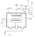
図4は、このような従来の化学蒸着装置の構成を示した正面概略図である。図4に示す装置は、排気系8を備えた真空容器1と、真空容器1内の所定の位置に処理される基板20を保持する基板ホルダー2と、基板20を所定温度に加熱する加熱手段3と、加熱された基板20の表面に原料ガスを供給する原料ガス供給系4とを備え、基板20の表面又は表面近傍における化学反応を利用して当該表面に所定の薄膜を作製するように構成されている。
【0004】
最近の金属材料の成膜では、常温常圧で液体である有機金属化合物を原料として使用するCVDが盛んに研究されている。例えば、配線用の金属材料の分野では、高マイグレーション耐性で、低比抵抗を有する銅(Cu)が次世代の配線材料として有力視されているが、CuのCVD成膜では、〔トリメチルビニルシリル〕ヘキサフルオロアセチルアセトン酸塩銅(以下、Cu(hfac)(tmvs)と略す)等の常温常圧で液体である有機金属化合物を原料として使用することがある。
【0005】
図4には、このような液体原料を使用する装置が例示されている。即ち、原料ガス供給系4は、液体原料を溜めた原料容器41から送液用配管411、バルブ412を介して送られる液体原料を気化させる気化器42と、気化器42で気化した原料ガスを真空容器1に送るガス導入用配管421、バルブ422や、不図示の流量調整器と、ガス導入用配管421の終端に接続するようにして真空容器1内に設けられたシャワーヘッド43とから主に構成されている。シャワーヘッド43は、ガス導入用配管421に連通した内部空間を有する円盤状の部材である。このシャワーヘッド43は、基板ホルダー2に保持された基板20に対向する面にガス吹き出し孔430を多数有して、ガス吹き出し孔430から原料ガスを吹き出させて真空容器1内に導入するようになっている。なお、原料ガス供給系4には、原料ガスを真空容器1に効率良く導くために原料ガスに混合するキャリアーガスを導入するキャリアーガス導入系5が接続されている。また、真空容器1の外壁面には、原料ガスの液化を防止するヒータ7が設けられている。
【0006】
上記構成に係る従来の化学蒸着装置の動作について、Cu(hfac)(tmvs)を原料として使用した銅のCVD成膜を例にとって説明する。まず、基板20を基板ホルダー2に支持させ、加熱手段3により100〜300℃程度の温度に基板2を加熱する。この状態で、Cu(hfac)(tmvs)を気化器42により気化させ、キャリアーガスとして水素ガス等を混合してシャワーヘッド43のガス吹き出し孔430から吹き出させて真空容器1内に導入する。導入されたCu(hfac)(tmvs)のガスは、基板20に到達し、分解を含む所定の反応が熱によって生じて基板20の表面にCuの膜が堆積する。
【0007】
【発明が解決しようとする課題】
上記構成に係る従来の化学蒸着装置においては、生産性の向上のため、成膜速度を上げることが重要な課題となっている。ここで、一般的に、化学蒸着装置において、化学反応は供給律速であり、薄膜を堆積する際の前駆体としての原料ガスの供給量によって成膜速度は決まる。また、従来の化学蒸着装置のように、常温常圧で液体の原料を使用する場合、原料ガスの供給量は、液体原料を気化させる気化器の気化効率に大きく依存している。
【0008】
気化効率を決める重要なパラメーターは、気化器内部の圧力であり、圧力が低い場合には気化効率は高いが、圧力が高くなるにつれて気化効率が低下する。従来の化学蒸着装置においては、このことが原料ガスの供給量を増加させることによって成膜速度を上げる上での重要な問題となっていた。
【0009】
この点については、図4にあるような従来のシャワーヘッドの方式から、特開平10−60650号で提案された方式により、下地として、スパッタリング法、又は、化学蒸着法のいずれかの手法で成膜されたCu膜上に成膜する場合、原料ガスが均一に、しかも、効率良く十分に供給できるようになったので、均一性の良い銅薄膜を、しかも、高い成膜速度で作製することが可能になった。特に、特開平10−60650号で提案された方式によれば、半導体の配線構造におけるトレンチ溝やビアホール等の埋め込み工程では、優れた特性が発揮されることが確認されている。
【0010】
ところで、半導体のCu配線の製造工程には、上記のようなCVD法による銅(Cu)の埋め込み工程とは別に、TiN、Ta、もしくはTaNなどのようなバリア膜上に、その後の工程となる電解メッキ等による埋め込み工程を良好なものにするため、500〜1000オングストロームの比較的薄いCu膜(シード膜、Seed膜)を形成させる工程がある。
【0011】
しかし、下地がTiN、Ta、TaN等のバリア膜上に薄いシード膜を形成する場合、膜形成の初期段階において、基板の周辺部においてCuの核の発生密度が小さくなり、この初期段階における状態は、最終的なCu膜の膜厚分布を決定してしまい、結果的に良質なシード膜としてのCu膜を得られないという新たな不具合が生じた。
【0012】
つまり、特開平10−60650号で提出された方式は、原料ガスを基板上へ均一で大量に供給することができるため、高速成膜実現の課題を解決したが、Cu膜上以外のTiN、Ta、TaN等の下地膜上に、500〜1000オングストロームの比較的薄いシード膜を形成する場合には、最終膜厚分布を決定してしまう初期段階の均一で高密度な核形成が困難であるという新たな改善すべき課題が残った。
【0013】
本発明は、前記のように残された新たな改善すべき課題の解決を目指すものである。
【0014】
【課題を解決するための手段】
前述した特開平10−60650号で提案されている基本的な構成の化学蒸着装置において、基板ホルダーに保持されている処理されるべき基板の表面に原料ガスを供給する原料ガス供給系の当該基板に対向して、なおかつその中心が当該基板の中心と同軸上になる位置に配置されているガス導入口の内径の、処理されるべき基板直径に対する好ましい比率を定めると共に、原料ガス導入口に連設されて前記処理されるべき基板側に向けて徐々に拡径しつつ開口しているガス供給室の前記基板に対向している内面に、複数の孔が穿設されている円盤状のガス整流板を、前記基板に対向して取り付けることによって前記課題の解決を図ったものである。
【0015】
すなわち、このようなCu膜の高速成膜を実現し得る構成を採用することによって、特開平10−60650号で提案されているガス供給室内面の特徴的な形状による作用とあいまって、ガス導入口から供給された原料ガスを、前記ガス整流板を通過した後、均一でしかも一定な流速を有する原料ガス流として基板に衝突させ、当該基板上で均一に、効率良く定着させて、基板全面に、なおかつ均一で高密度な、初期の核形成を進行させるようにしたのである。
【0016】
【作用】
すなわち、本発明が提案する化学蒸着装置は、排気系を有する真空容器と、真空容器内の所定の位置に処理される基板を保持する基板ホルダーと、当該基板を所定温度に加熱する加熱手段と、当該基板に対向する位置に原料ガス導入口を有していて、加熱された当該基板の表面に原料ガスを供給する原料ガス供給系とを備えている点、また、イ)原料ガス供給系の前記原料ガス導入口は、その中心軸が前記処理される基板の中心と同軸上になる位置に配置されており、当該原料ガス導入口に前記処理される基板側に向けて徐々に拡径しつつ開口しているガス供給室が連設されており、ロ)当該ガス供給室の前記基板に対向している内面は、前記原料ガス導入口の中心軸上に頂点を有する円錐の傾斜面を成している、あるいは、ロ)当該ガス供給室の前記基板に対向している内面は、前記原料ガス導入口の中心軸上に頂点を有する円錐状の曲面を成して、当該内面の任意の点における前記原料ガス導入口の中心軸からの距離をr、その点における前記基板との距離をhとしたとき、rとhの積がrの大きさにかかわらずほぼ一定である双曲線を、前記原料ガス導入口の中心軸の回りに回転させて得られる回転双曲面に形成されている構成を採用し、これらによって、原料ガスを処理すべき基板上へ均一に、しかも大量に供給できる構造としている点において、特開平10−60650号で提出された方式と同様である。
【0017】
そして、本発明が提案する化学蒸着装置は、このような構成の化学蒸着装置において、更に、ハ)前記ガス導入口の内径の、処理される基板の直径に対する比は1/12乃至1/8であり、ニ)前記ガス供給室の前記基板に対向している内面に、複数の孔が穿設されている円盤状のガス整流板が、前記基板に対向して取り付けられている、という特徴的な構成を具備しているものである。
【0018】
すなわち、本発明が提案する化学蒸着装置は、ガス供給室の前記基板に対向している内面(以下「対向面」という)が、流体力学の観点から設計された円錐の傾斜面または円錐状の曲面を成している点で、特開平10−60650号で提出された方式と同様であり、原料ガスを処理すべき基板へ均一にしかも大量に供給できる構造は、特開平10−60650号で提案された考え方を採用したものである。
【0019】
本発明の化学蒸着装置に特徴的な、ガス供給室の対向面に、基板に対向して取り付けられている、複数の孔が穿設されている円盤状のガス整流板によって、本発明の化学蒸着装置におけるガス供給室は、基板に向かっている開口側が前記円盤状のガス整流板によって塞がれている、いわば漏斗状の形状となっている(図1)。ガス導入用配管の終端であるガス導入口から基板ホルダー側に向かって、漏斗状に広がるガス供給室の対向面が、基板と対向する位置で、複数の穴が穿設されているガス整流板により仕切られるため、ガス供給室内に充満する高濃度の原料ガスは、漏斗状形態の効果により、ガス整流板を通過した後、均一でしかも一定な流速を有する原料ガス流となって、基板に衝突する。その結果、衝突した原料ガスは、基板上に、均一に効率良く定着するため、基板全面に均一でしかも高密度な初期の核形成を進行させることが可能になるのである。
【0020】
ここで、本発明の化学蒸着装置において、ガス導入口の内径の、処理されるべき基板の直径に対する比を1/12乃至1/8とする理由は、常温常圧で液体の原料を気化する気化器の気化効率を低下させないと共に、最適のコンダクタンス及び処理されるべき基板上への均一で、一定な流速を有する原料ガス流を実現させる上で、好ましいからである。具体的には、前記比率の下限は、気化器の気化効率を低下させないという観点から定められ、200mmのSi基板に成膜する場合には、ガス導入口の内径を17mm以上、300mmのSi基板に成膜する場合には、ガス導入口の内径を25mm以上とすることが好ましい。一方、前記比率の上限は、最適のコンダクタンス及び処理されるべき基板上への均一で、一定な流速を有する原料ガス流を実現させるという観点から定められ、200mmのSi基板に成膜する場合には、ガス導入口の内径を25mm以下、300mmのSi基板に成膜する場合には、ガス導入口の内径を37.5mm以下とすることが好ましい。
【0021】
なお、前記の本発明の化学蒸着装置において、ガス整流板の直径の、ガス導入口の内径に対する比は、常温常圧で液体の原料を気化する気化器の気化効率を低下させないと共に、最適のコンダクタンス及び処理されるべき基板上への均一で、一定な流速を有する原料ガス流を実現させる上で、8乃至12としておくことが望ましい。
【0022】
【発明の実施の形態】
以下、添付図面を参照して本発明の好ましい実施の形態を説明する。
【0023】
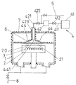
図1に示す装置は、排気系8を備えた真空容器1と、真空容器1内の所定の位置に処理する基板20を保持する基板ホルダー2と、基板20を所定温度に加熱する加熱手段3と、加熱された基板20の表面に原料ガスを供給する原料ガス供給系4とを備え、基板20の表面における化学反応を利用して当該表面に所定の銅薄膜を作製するよう構成されている。
【0024】
真空容器1は、不図示のゲートバルブ等を備えた気密な容器である。真空容器1の外壁面にはヒータ7が付設されている。このヒータ7は、後述する原料ガス供給系4により供給された原料ガスが真空容器1の内壁面で結露しないよう、真空容器1を加熱するためのものである。排気系8は、油拡散ポンプやターボ分子ポンプなどの真空ポンプ(図示していない)を備えて、真空容器1内を1×10⁻²Pa程度以下の圧力まで排気可能に構成されている。
【0025】
基板ホルダー2は、上面に基板20を載置して保持するものであり、静電気により基板20を吸着する不図示の静電吸着機構が必要に応じて設けられる。加熱手段3は、例えば、抵抗加熱方式のものが使用され、所定の化学反応を生ずるのに必要な温度に基板20を加熱する。例えば、原料が、Cu(hfac)(tmvs)である場合、150℃〜250℃程度の範囲で加熱する。
【0026】
図1図示の装置は、例えば、Cu(hfac)(tmvs)のような常温常圧で液体である原料を使用するものであり、原料ガス供給系4は、この液体の原料を気化させて基板20に供給するよう構成されている。具体的には、原料ガス供給系4は、液体である原料を溜めた原料容器41と、原料容器41から送液用配管411、バルブ412を介して運ばれた液体原料を気化させる気化器42、気化器42で気化させた原料をガス導入用配管421、バルブ422を介して真空容器1内に導く構成になっている。なお、送液用配管411、バルブ412によって繋がれている原料容器41と気化器42との間、ガス導入用配管421、バルブ422によって繋がれている気化器42と真空容器1との間には、それぞれ、不図示の液体流量調整器等を設けることができる。また、原料ガス供給系4には、原料ガスを真空容器1に効率良く導くために原料ガスに混合するキャリアーガスを導入するキャリアーガス導入系5が接続されている。また、ガス導入用配管421には、ヒータ423が付設されており、ガス導入用配管421の温度を所定の温度に加熱して内部での原料ガスの液化を防止するようになっている。
【0027】
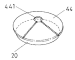
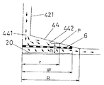
ガス導入用配管421の終端であるガス導入口441は、基板20の中心と同軸上に位置し、このガス導入口441には、基板ホルダー2に向かって、漏斗状に拡径しつつ開口するガス供給室44が連設されている。すなわち、ガス供給室44の対向面442は、基板の中心と同軸上に頂点を有する円錐の斜面、もしくは、円錐状の曲面の一部を成す形状となっている。
【0028】
図1、図3図示の装置においては、ガス供給室44の対向面442は、基板の中心と同軸上に頂点を有する円錐の斜面として形成され、図2図示の装置においては、ガス供給室44の対向面442は、円錐状の曲面の一部を成す形状、すなわち、対向面442における任意の点(P)の基板中心軸(すなわち、ガス導入口441の中心軸)からの距離をr、その点Pにおける基板20との距離をhとしたとき、rとhの積がrの大きさにかかわらずほぼ一定である双曲線を基板20の中心(すなわち、ガス導入口441の中心)と同軸上の回転軸の回りに回転させて得られる回転双曲面になっている。
【0029】
以上説明した本発明の化学蒸着装置の基本的な構成は、特開平10−60650号で提案されている構成と同様である。
【0030】
本発明の化学蒸着装置に特徴的な構成は、ガス導入口441の内径の、基板20の直径に対する比が1/12乃至1/8に定められており、更に、ガス供給室44の内面の基板20と対向する位置に、複数の穴が穿設されたガス整流板6が取り付けられている点にある。
【0031】
こうしてガス整流板6によって仕切られた、その下側(基板20側)が薄膜形成領域21になる。
【0032】
尚、本発明の化学蒸着装置を構成する材質については、ガス整流板6を除いたガス供給室44は、ステンレスやアルミニウム、銅等の金属で形成され、表面がアルマイト処理されていても構わない。ガス整流板との接合性に問題が無ければ、石英製の場合もある。
【0033】
次に、図3を用いてガス整流板6について説明する。図3は、ガス供給室44の対向面442が、基板の中心と同軸上に頂点を有する円錐の斜面として形成されている実施例を表すものであるが、以下の説明は、ガス供給室44の対向面442が、原料ガス導入口441の中心軸上に頂点を有する円錐状の曲面を成して、対向面442の任意の点における原料ガス導入口441の中心軸からの距離をr、その点における基板20との距離をhとしたとき、rとhの積がrの大きさにかかわらずほぼ一定である双曲線を、原料ガス導入口441の中心軸の回りに回転させて得られる回転双曲面に形成されている場合にも適用されるものである。
【0034】
ガス整流板6の大きさ(直径=2×半径:R)は、基板20の直径(2×半径:W)とほぼ同等である。
【0035】
本願発明のようなガス整流板6を用いない場合では、前述のとおり、下地がTiN、Ta、TaN等のバリア膜上に薄いシード膜を形成するとき、Cu(銅)膜形成の初期段階において、基板20の周辺部のCuの核発生密度が小さくなる。その原因については、現在十分解明されていないが、次のように推定されている。つまり、本願発明のようなガス整流板6を用いない場合、ガス導入口441から噴出した高濃度の新しい原料ガス流は、常に基板周辺部よりも先に基板中央部の表面に衝突するため、基板中央部では周辺部に比べ、先に核形成が進行してしまう。しかし、本願発明のようなガス整流板6がある場合には、高濃度の原料ガスを均一で、しかも一定の流速を有する原料ガス流の状態で基板20に衝突させることが可能となる。
【0036】
従って、基板全面への均一な原料ガス流の供給が確保されることにより、ガス整流板6の大きさ(直径)は、高価な原料ガスの最適な消費効率上、必要以上に大口径にする必要がなく、前記の通り基板20の大きさ(直径)とほぼ同程度であればよい。
【0037】
ガス整流板6の厚さについては、構造的な強度の面と後述のコンダクタンスとの関係で、5〜15mm程度で、材質については、熱伝導性の良い銅、もしくは、アルミニウム、もしくはこれらを主成分とする合金が望ましい。
【0038】
又、ガス整流板6は、不図示のクリーニングガス用のガス導入系により、in−situで定期的なクリーニングをすることが可能であるが、最も簡略なねじ止め方式等の、機械的にガス供給室44から取り外しが可能な構造を有することもできる。
【0039】
ガス整流板6に穿設される孔についてであるが、コンダクタンスの面からは、常温常圧で液体の原料を気化する気化器の気化効率を低下させないと共に、最適のコンダクタンス及び処理されるべき基板20上への均一で、一定な流速を有する原料ガス流を実現させるという観点から、その内径の基板20の直径に対する比が1/12乃至1/8に定められているガス導入口441にガス供給室44が接続されるのであるから、当該ガス導入口441及びこれに接続されているガス導入用配管421と同じコンダクタンスを持つように、ガス整流板6に複数の孔を穿設すれば十分である。
【0040】
しかし、実際には、等コンダクタンスより、少しコンダクタンスを小さめにして、僅かな圧力差を持たせた方が、基板20上に良好なCuの初期的な核形成を実現できる。実際にはガス導入口441におけるコンダクタンスに対して、1/2〜1/3ぐらいのコンダクタンスをガス整流板6が有するように、ガス整流板6に穿設される孔を形成することが、基板20上に良好なCuの初期的な核形成を実現させる上で、望ましい。
【0041】
具体的には、ガス導入口441の内径の基板20直径に対する比が1/12乃至1/8で(すなわち、ガス導入口441の内径のガス整流板6の直径に対する比が1/12乃至1/8で)、ガス整流板6の厚みが10mmであり、形状が円筒形を想定した場合、ガス整流板6に設ける孔は、φ1.5mmのとき、約5mm間隔で、φ2.0mmのとき、ほぼ8〜10mm間隔で配列させると、上述の所望のコンダクタンスが得られる。
【0042】
次に、本実施形態の装置の全体の動作を図1、2により説明する。
【0043】
まず、不図示のゲートバルブを通して基板20を真空容器1内に搬入し、基板ホルダー2の表面に載置して保持させる。この際、加熱手段3が、予め動作して基板ホルダー2を加熱しており、基板20は、基板ホルダー2に載置されることで、150℃から250℃程度の範囲の温度に加熱される。並行して、排気系8が動作して真空容器1内を1×10⁻²Pa程度まで排気した後、原料ガス供給系4を動作させ、原料ガスを基板20に供給する。尚、真空容器1に、ロードロックチャンバー等の補助チャンバーが配設される場合、補助チャンバーと真空容器1内と同程度の圧力まで排気した後、基板20を補助チャンバーから真空容器1内に搬入し、その後ゲートバルブを閉じて原料ガスを供給するようにする。
【0044】
このように、本実施形態の装置によれば、図4図示の従来装置のようなシャワーヘッドを使用せず、気化器42による気化効率を低下させない十分な内径を有するガス導入口441を使用することで、この近傍の圧力上昇を防止することができる。このため、気化器42内の圧力が高くなることが抑制され、気化器42の気化効率を高く維持することができる。しかも、流体力学的検討を基に設計された漏斗状のガス供給室44、および、その上で、ガス導入口441に繋がるガス導入用配管のコンダクタンスとの関係を考慮して前述のように定められているガス整流板6のコンダクタンスにより、ガス整流板6を通過する原料ガス流を、均一でしかも一定な流速として、基板20に衝突させることができる。その結果、基板20上に衝突した原料ガスは、均一に、効率良く定着するため、確実に高密度な初期の核形成が進行する。
【0045】
尚、成膜の具体例について、原料ガスとして、上述したCu(hfac)(tmvs)を用いて銅の薄膜を作製する場合を例にとって説明すると、Cu(hfac)(tmvs)を0.17g/min.の流量で供給し、基板20を温度170℃に設定し、成膜圧力を2kPaとした。初期段階の核形成の効果を確認するため、200mmのSi基板に下地としてスパッタリングにより2000オングストロームのTiN膜を作製し、その上に、銅(Cu)を比較的薄く500オングストロームの厚みで成膜した。
【0046】
結果は、肉眼的にも明らかに、銅特有の金属光沢を有する、均一な鏡面状の成膜ができていることを確認できた。
【0047】
以上、添付図面を参照して本発明の好ましい実施の形態を説明したが、本発明は、前述した実施形態に限定されるものではなく、特許請求の範囲に記載した技術的思想の創作の範囲内で種々の態様に変更可能である。
【0048】
【発明の効果】
本発明の形態の装置によれば、最適なコンダクタンスを得つつ、常温常圧で液体の原料を気化させる気化器の気化効率を高く維持することができるため、原料ガスの供給量を高めることができ、しかも、流体力学的に計算されて設計された「漏斗」状のガス供給室と最適なコンダクタンスを有するガス整流板とを組み合わせて使用することにより、均一で一定の流速を有する原料ガス流を対向する基板上に衝突させることができ、その結果、半導体製造工程における薄い銅(Cu)のシード層形成のような、下地がCu以外の基板上に対しても、均一で高密度なCuの初期の核形成が可能となり、このシード層上に引き続きCuを堆積させた結果、200mmSi基板で最終膜厚分布(Cu膜厚:1500オングストローム)を測定したところ、±5%前後の良好な値を示した。しかも、銅の金属光沢を有する均一な鏡面状のCu膜を作製することができる。
【図面の簡単な説明】
【図1】この発明の化学蒸着装置の好ましい実施例の構成を説明する正面概略図。
【図2】この発明の他の化学蒸着装置の好ましい実施例に採用されたガス供給室の構成を説明する一部を破切し、一部を省略した概略斜視図。
【図3】図1に示す装置に採用されたガス供給室の構成及び作用を説明する模式図。
【図4】従来の化学蒸着装置の構成を説明する正面概略図。
【符号の説明】
1 真空容器
2 基板ホルダー
3 加熱手段
4 原料ガス供給系
6 ガス整流板
8 排気系
20 基板
44 ガス供給室
441 ガス導入口[0001]
BACKGROUND OF THE INVENTION
The invention of the present application relates to a chemical vapor deposition apparatus that uses an organometallic compound that is liquid at normal temperature and pressure as a raw material, vaporizes this, and uses a chemical reaction of a reactive gas to produce a Cu (copper) thin film.
[0002]
[Prior art]
In the manufacture of a large scale integrated circuit (LSI), a liquid crystal display (LCD), etc., there is a step of forming a predetermined thin film on the surface of a substrate. In the production of such a thin film, since a thin film having a required composition can be produced relatively freely, a chemical vapor deposition method (CVD) for producing a thin film using a chemical reaction of a reactive gas is widely used. ing.
[0003]
FIG. 4 is a schematic front view showing the configuration of such a conventional chemical vapor deposition apparatus. The apparatus shown in FIG. 4 includes a
[0004]
In the recent film formation of metal materials, CVD using an organometallic compound that is liquid at normal temperature and pressure as a raw material has been actively studied. For example, in the field of metal materials for wiring, copper (Cu) having high migration resistance and low specific resistance is regarded as a promising next-generation wiring material. An organometallic compound that is liquid at normal temperature and pressure, such as copper hexafluoroacetylacetonate (hereinafter abbreviated as Cu (hfac) (tmvs)), may be used as a raw material.
[0005]
FIG. 4 illustrates an apparatus using such a liquid raw material. That is, the raw material
[0006]
The operation of the conventional chemical vapor deposition apparatus according to the above configuration will be described by taking, as an example, a CVD film formation of copper using Cu (hfac) (tmvs) as a raw material. First, the
[0007]
[Problems to be solved by the invention]
In the conventional chemical vapor deposition apparatus having the above-described configuration, it is an important issue to increase the film forming speed in order to improve productivity. Here, in general, in a chemical vapor deposition apparatus, a chemical reaction is rate-controlled, and a film formation rate is determined by a supply amount of a source gas as a precursor when a thin film is deposited. In addition, when a liquid source is used at normal temperature and pressure as in a conventional chemical vapor deposition apparatus, the supply amount of the source gas largely depends on the vaporization efficiency of the vaporizer that vaporizes the liquid source.
[0008]
An important parameter for determining the vaporization efficiency is the pressure inside the vaporizer. The vaporization efficiency is high when the pressure is low, but the vaporization efficiency decreases as the pressure increases. In the conventional chemical vapor deposition apparatus, this has been an important problem in increasing the deposition rate by increasing the supply amount of the source gas.
[0009]
With respect to this point, the conventional shower head method as shown in FIG. 4 is used as a base by either the sputtering method or the chemical vapor deposition method according to the method proposed in Japanese Patent Laid-Open No. 10-60650. When forming a film on a Cu film, the source gas can be supplied uniformly and efficiently and sufficiently, so that a copper thin film with good uniformity can be produced at a high film formation rate. Became possible. In particular, according to the method proposed in Japanese Patent Laid-Open No. 10-60650, it has been confirmed that excellent characteristics are exhibited in a filling process of a trench groove, a via hole or the like in a semiconductor wiring structure.
[0010]
By the way, the manufacturing process of the Cu wiring of the semiconductor is a subsequent process on the barrier film such as TiN, Ta, or TaN separately from the copper (Cu) embedding process by the CVD method as described above. In order to improve the embedding process by electrolytic plating or the like, there is a process of forming a relatively thin Cu film (seed film, seed film) of 500 to 1000 angstroms.
[0011]
However, when a thin seed film is formed on a barrier film made of TiN, Ta, TaN or the like as a base, the generation density of Cu nuclei is reduced in the peripheral part of the substrate in the initial stage of film formation. As a result, the film thickness distribution of the final Cu film was determined, and as a result, a new defect that a Cu film as a high-quality seed film could not be obtained occurred.
[0012]
In other words, the method submitted in Japanese Patent Laid-Open No. 10-60650 solved the problem of realizing high-speed film formation because the source gas can be supplied uniformly and in large quantities onto the substrate, but TiN other than on the Cu film, When a relatively thin seed film of 500 to 1000 angstroms is formed on a base film such as Ta or TaN, it is difficult to form uniform and high-density nuclei at the initial stage that determines the final film thickness distribution. There remains a new issue to be improved.
[0013]
The present invention aims to solve a new problem to be improved that remains as described above.
[0014]
[Means for Solving the Problems]
In the chemical vapor deposition apparatus having the basic configuration proposed in Japanese Patent Laid-Open No. 10-60650 described above, the substrate of the source gas supply system that supplies source gas to the surface of the substrate to be processed held by the substrate holder In addition, a preferable ratio of the inner diameter of the gas inlet arranged at the position where the center thereof is coaxial with the center of the substrate to the diameter of the substrate to be processed is determined, and connected to the source gas inlet. A disk-shaped gas having a plurality of holes drilled on the inner surface facing the substrate of the gas supply chamber that is open while gradually expanding in diameter toward the substrate to be processed The rectifying plate is attached to face the substrate to solve the above problem.
[0015]
That is, by adopting a configuration capable of realizing high-speed deposition of such a Cu film, combined with the action due to the characteristic shape of the gas supply chamber surface proposed in JP-A-10-60650, gas introduction After passing through the gas rectifying plate, the source gas supplied from the mouth is collided with the substrate as a source gas flow having a uniform and constant flow rate, and uniformly and efficiently fixed on the substrate, In addition, the initial nucleation was advanced in a uniform and high density.
[0016]
[Action]
That is, the chemical vapor deposition apparatus proposed by the present invention includes a vacuum vessel having an exhaust system, a substrate holder that holds a substrate to be processed at a predetermined position in the vacuum vessel, and a heating unit that heats the substrate to a predetermined temperature. And a source gas supply system that has a source gas inlet at a position facing the substrate and supplies source gas to the heated surface of the substrate, and a) a source gas supply system. The raw material gas inlet is disposed at a position where its central axis is coaxial with the center of the substrate to be processed, and the diameter of the raw material gas inlet gradually increases toward the substrate to be processed. However, an open gas supply chamber is continuously provided, and b) an inner surface of the gas supply chamber facing the substrate is a conical inclined surface having a vertex on the central axis of the source gas inlet Or b) the gas supply The inner surface of the chamber facing the substrate forms a conical curved surface having a vertex on the central axis of the raw material gas inlet, from the central axis of the raw material gas inlet at an arbitrary point on the inner surface. Where r is the distance of the substrate and h is the distance from the substrate at that point, a hyperbola in which the product of r and h is substantially constant regardless of the magnitude of r is around the central axis of the source gas inlet. JP, 10-60650, A adopts the structure formed in the rotation hyperboloid obtained by rotating, and makes it the structure which can supply source gas uniformly and in large quantities to the substrate which should be processed by these. This is the same as the method submitted in.
[0017]
In the chemical vapor deposition apparatus proposed by the present invention, in the chemical vapor deposition apparatus having such a configuration, c) the ratio of the inner diameter of the gas inlet to the diameter of the substrate to be processed is 1/12 to 1/8. And d) a disc-shaped gas rectifying plate having a plurality of holes drilled on the inner surface of the gas supply chamber facing the substrate, which is mounted facing the substrate. It has a typical configuration.
[0018]
That is, in the chemical vapor deposition apparatus proposed by the present invention, the inner surface of the gas supply chamber facing the substrate (hereinafter referred to as “opposing surface”) has a conical inclined surface or conical shape designed from the viewpoint of hydrodynamics. Similar to the method submitted in Japanese Patent Laid-Open No. 10-60650 in that it has a curved surface, a structure capable of supplying a source gas uniformly and in large quantities to a substrate to be processed is disclosed in Japanese Patent Laid-Open No. 10-60650. The proposed concept is adopted.
[0019]
A disc-shaped gas rectifying plate having a plurality of holes drilled on the opposite surface of the gas supply chamber, which is characteristic of the chemical vapor deposition device of the present invention, is attached to the opposite surface of the gas supply chamber. The gas supply chamber in the vapor deposition apparatus has a so-called funnel shape in which the opening side toward the substrate is closed by the disk-shaped gas rectifying plate (FIG. 1). A gas rectifying plate in which a plurality of holes are perforated at a position where the opposing surface of the gas supply chamber extending in a funnel shape faces the substrate from the gas introduction port, which is the end of the gas introduction pipe, to the substrate Therefore, the high-concentration source gas filling the gas supply chamber becomes a source gas flow having a uniform and constant flow rate after passing through the gas rectifying plate due to the effect of the funnel-like shape. collide. As a result, the colliding source gas is uniformly and efficiently fixed on the substrate, so that it is possible to advance initial and uniform nucleation over the entire surface of the substrate.
[0020]
Here, in the chemical vapor deposition apparatus of the present invention, the reason why the ratio of the inner diameter of the gas inlet to the diameter of the substrate to be processed is 1/12 to 1/8 is that the liquid raw material is vaporized at normal temperature and pressure. This is because the vaporization efficiency of the vaporizer is not lowered, and it is preferable to realize a source gas flow having an optimum conductance and a uniform and constant flow rate on the substrate to be processed. Specifically, the lower limit of the ratio is determined from the viewpoint of not lowering the vaporization efficiency of the vaporizer. When the film is formed on a 200 mm Si substrate, the gas inlet has an inner diameter of 17 mm or more and a 300 mm Si substrate. In the case of film formation, the inner diameter of the gas inlet is preferably 25 mm or more. On the other hand, the upper limit of the ratio is determined from the viewpoint of realizing an optimal conductance and a raw material gas flow having a uniform and constant flow rate on the substrate to be processed, and when the film is formed on a 200 mm Si substrate. In the case of forming a film on a Si substrate having an inner diameter of 25 mm or less and 300 mm, the inner diameter of the gas introduction port is preferably 37.5 mm or less.
[0021]
In the above-described chemical vapor deposition apparatus of the present invention, the ratio of the diameter of the gas flow straightening plate to the inner diameter of the gas inlet does not decrease the vaporization efficiency of the vaporizer that vaporizes the liquid raw material at normal temperature and pressure, and is optimal. In order to realize a conductance and a raw material gas flow having a uniform and constant flow rate on the substrate to be processed, it is desirable to set 8 to 12.
[0022]
DETAILED DESCRIPTION OF THE INVENTION
Hereinafter, preferred embodiments of the present invention will be described with reference to the accompanying drawings.
[0023]
The apparatus shown in FIG. 1 includes a
[0024]
The
[0025]
The
[0026]
The apparatus shown in FIG. 1 uses a raw material that is liquid at room temperature and normal pressure, such as Cu (hfac) (tmvs), and the raw material
[0027]
The
[0028]
In the apparatus shown in FIGS. 1 and 3, the opposing surface 442 of the
[0029]
The basic configuration of the chemical vapor deposition apparatus of the present invention described above is the same as the configuration proposed in JP-A-10-60650.
[0030]
The characteristic structure of the chemical vapor deposition apparatus of the present invention is that the ratio of the inner diameter of the
[0031]
The lower side (
[0032]
In addition, about the material which comprises the chemical vapor deposition apparatus of this invention, the
[0033]
Next, the
[0034]
The size (diameter = 2 × radius: R) of the
[0035]
In the case where the
[0036]
Therefore, by ensuring supply of a uniform raw material gas flow to the entire surface of the substrate, the size (diameter) of the
[0037]
The thickness of the
[0038]
Further, the
[0039]
As for the holes drilled in the
[0040]
However, in practice, better initial nucleation of Cu can be realized on the
[0041]
Specifically, the ratio of the inner diameter of the
[0042]
Next, the overall operation of the apparatus of this embodiment will be described with reference to FIGS.
[0043]
First, the
[0044]
As described above, according to the apparatus of the present embodiment, the shower head as in the conventional apparatus shown in FIG. 4 is not used, and the
[0045]
A specific example of film formation will be described by taking as an example the case where a copper thin film is formed using the above-described Cu (hfac) (tmvs) as a source gas. Cu (hfac) (tmvs) is 0.17 g / min. The
[0046]
The results clearly confirmed that a uniform mirror-like film having a metallic luster unique to copper was formed.
[0047]
The preferred embodiments of the present invention have been described above with reference to the accompanying drawings, but the present invention is not limited to the above-described embodiments, and the scope of creation of the technical idea described in the claims. It can be changed in various ways.
[0048]
【The invention's effect】
According to the apparatus of the present invention, it is possible to maintain a high vaporization efficiency of a vaporizer that vaporizes a liquid raw material at room temperature and normal pressure while obtaining optimum conductance. In addition, by using a combination of a “funnel” -shaped gas supply chamber designed and calculated hydrodynamically and a gas rectifying plate having an optimum conductance, a feed gas flow having a uniform and constant flow rate can be obtained. Can be made to collide on the opposite substrate, and as a result, even if the substrate is a substrate other than Cu, such as formation of a thin copper (Cu) seed layer in the semiconductor manufacturing process, uniform and high-density Cu As a result of subsequent Cu deposition on this seed layer, the final film thickness distribution (Cu film thickness: 1500 Å) was measured on a 200 mm Si substrate. Showed good values of around 5% ±. In addition, a uniform mirror-like Cu film having a metallic luster of copper can be produced.
[Brief description of the drawings]
FIG. 1 is a schematic front view illustrating the configuration of a preferred embodiment of a chemical vapor deposition apparatus according to the present invention.
FIG. 2 is a schematic perspective view in which a part of the configuration of a gas supply chamber employed in a preferred embodiment of another chemical vapor deposition apparatus of the present invention is cut off and a part thereof is omitted.
3 is a schematic diagram for explaining the configuration and operation of a gas supply chamber employed in the apparatus shown in FIG.
FIG. 4 is a schematic front view illustrating the configuration of a conventional chemical vapor deposition apparatus.
[Explanation of symbols]
DESCRIPTION OF
Claims (2)
イ)原料ガス供給系の前記原料ガス導入口は、その中心軸が前記処理される基板の中心と同軸上になる位置に配置されていて、当該原料ガス導入口に前記処理される基板側に向けて徐々に拡径しつつ開口しているガス供給室が連設されており、
ロ)当該ガス供給室の前記基板に対向している内面は、前記原料ガス導入口の中心軸上に頂点を有する円錐の傾斜面を成し、
ハ)前記ガス導入口の内径の、処理される基板の直径に対する比は1/12乃至1/8であり、
ニ)前記ガス供給室の前記基板に対向している内面に、複数の孔が穿設されている円盤状で前記基板と同等の大きさを有するガス整流板が、前記基板に対向して取り付けられており、前記ガス整流板に穿設されている複数の孔のコンダクタンスは、前記ガス導入口におけるコンダクタンスの1/2〜1/3である。 A vacuum vessel having an exhaust system, a substrate holder for holding a substrate to be processed at a predetermined position in the vacuum vessel, a heating means for heating the substrate to a predetermined temperature, and a source gas inlet at a position facing the substrate And a raw material gas supply system for supplying a raw material gas to the heated surface of the substrate, and further vaporizing a liquid material having the following characteristics to form a copper thin film on the substrate Chemical vapor deposition equipment.
B) The source gas inlet of the source gas supply system is disposed at a position where the central axis is coaxial with the center of the substrate to be processed, and the source gas inlet is connected to the substrate to be processed. A gas supply chamber that opens while gradually expanding the diameter toward the
B) The inner surface of the gas supply chamber facing the substrate forms a conical inclined surface having an apex on the central axis of the source gas inlet,
C) The ratio of the inner diameter of the gas inlet to the diameter of the substrate to be processed is 1/12 to 1/8,
D) A gas rectifying plate having a disk-like shape in which a plurality of holes are formed on the inner surface of the gas supply chamber facing the substrate and having a size equivalent to that of the substrate is mounted facing the substrate. The conductance of the plurality of holes formed in the gas rectifying plate is 1/2 to 1/3 of the conductance at the gas inlet.
イ)原料ガス供給系の前記原料ガス導入口は、その中心軸が前記処理される基板の中心と同軸上になる位置に配置されていて、当該原料ガス導入口に前記処理される基板側に向けて徐々に拡径しつつ開口しているガス供給室が連設されており、
ロ)当該ガス供給室の前記基板に対向している内面は、前記原料ガス導入口の中心軸上に頂点を有する円錐状の曲面を成して、当該内面の任意の点における前記原料ガス導入口の中心軸からの距離をr、その点における前記基板との距離をhとしたとき、rとhの積がrの大きさにかかわらずほぼ一定である双曲線を、前記原料ガス導入口の中心軸の回りに回転させて得られる回転双曲面に形成されており、
ハ)前記ガス導入口の内径の、処理される基板の直径に対する比は1/12乃至1/8であり、
ニ)前記ガス供給室の前記基板に対向している内面に、複数の孔が穿設されている円盤状で前記基板と同等の大きさを有するガス整流板が、前記基板に対向して取り付けられており、前記ガス整流板に穿設されている複数の孔のコンダクタンスは、前記ガス導入口におけるコンダクタンスの1/2〜1/3である。 A vacuum vessel having an exhaust system, a substrate holder for holding a substrate to be processed at a predetermined position in the vacuum vessel, a heating means for heating the substrate to a predetermined temperature, and a source gas inlet at a position facing the substrate And a raw material gas supply system for supplying a raw material gas to the heated surface of the substrate, and further vaporizing a liquid material having the following characteristics to form a copper thin film on the substrate Chemical vapor deposition equipment.
B) The source gas inlet of the source gas supply system is disposed at a position where the central axis is coaxial with the center of the substrate to be processed, and the source gas inlet is connected to the substrate to be processed. A gas supply chamber that opens while gradually expanding the diameter toward the
(B) The inner surface of the gas supply chamber facing the substrate forms a conical curved surface having a vertex on the central axis of the source gas inlet, and the source gas introduction at an arbitrary point on the inner surface When the distance from the center axis of the mouth is r, and the distance from the substrate at that point is h, a hyperbola in which the product of r and h is substantially constant regardless of the magnitude of r is represented by the source gas inlet. It is formed into a rotating hyperboloid obtained by rotating around the central axis,
C) The ratio of the inner diameter of the gas inlet to the diameter of the substrate to be processed is 1/12 to 1/8,
D) A gas rectifying plate having a disk-like shape in which a plurality of holes are formed on the inner surface of the gas supply chamber facing the substrate and having a size equivalent to that of the substrate is mounted facing the substrate. The conductance of the plurality of holes formed in the gas rectifying plate is 1/2 to 1/3 of the conductance at the gas inlet.
Priority Applications (1)
| Application Number | Priority Date | Filing Date | Title |
|---|---|---|---|
| JP33776399A JP4635266B2 (en) | 1999-11-29 | 1999-11-29 | Chemical vapor deposition equipment |
Applications Claiming Priority (1)
| Application Number | Priority Date | Filing Date | Title |
|---|---|---|---|
| JP33776399A JP4635266B2 (en) | 1999-11-29 | 1999-11-29 | Chemical vapor deposition equipment |
Publications (2)
| Publication Number | Publication Date |
|---|---|
| JP2001152344A JP2001152344A (en) | 2001-06-05 |
| JP4635266B2 true JP4635266B2 (en) | 2011-02-23 |
Family
ID=18311745
Family Applications (1)
| Application Number | Title | Priority Date | Filing Date |
|---|---|---|---|
| JP33776399A Expired - Lifetime JP4635266B2 (en) | 1999-11-29 | 1999-11-29 | Chemical vapor deposition equipment |
Country Status (1)
| Country | Link |
|---|---|
| JP (1) | JP4635266B2 (en) |
Families Citing this family (2)
| Publication number | Priority date | Publication date | Assignee | Title |
|---|---|---|---|---|
| JP5792364B1 (en) * | 2014-07-31 | 2015-10-07 | 株式会社日立国際電気 | Substrate processing apparatus, chamber lid assembly, semiconductor device manufacturing method, program, and recording medium |
| CN113140480A (en) * | 2020-01-19 | 2021-07-20 | 聚昌科技股份有限公司 | Wafer heating module with upper cover guide plate for improving temperature uniformity |
Family Cites Families (5)
| Publication number | Priority date | Publication date | Assignee | Title |
|---|---|---|---|---|
| JPH062948B2 (en) * | 1986-09-27 | 1994-01-12 | 東京エレクトロン株式会社 | How to treat the object |
| JPS6447029U (en) * | 1987-09-17 | 1989-03-23 | ||
| JP3414475B2 (en) * | 1994-02-25 | 2003-06-09 | スタンレー電気株式会社 | Crystal growth equipment |
| JP3901252B2 (en) * | 1996-08-13 | 2007-04-04 | キヤノンアネルバ株式会社 | Chemical vapor deposition equipment |
| JPH1180959A (en) * | 1997-09-08 | 1999-03-26 | Sony Corp | Vapor growth apparatus |
-
1999
- 1999-11-29 JP JP33776399A patent/JP4635266B2/en not_active Expired - Lifetime
Also Published As
| Publication number | Publication date |
|---|---|
| JP2001152344A (en) | 2001-06-05 |
Similar Documents
| Publication | Publication Date | Title |
|---|---|---|
| JP3901252B2 (en) | Chemical vapor deposition equipment | |
| JP4919534B2 (en) | Thermal CVD of TaN films from tantalum halide precursors | |
| TWI251619B (en) | Low-pressure deposition of metal layers from metal-carbonyl precursors | |
| US7955972B2 (en) | Methods for growing low-resistivity tungsten for high aspect ratio and small features | |
| TW317000B (en) | ||
| JPS59179775A (en) | Method and device for depositting tungsten silicide | |
| JP2002543284A (en) | PECVD of TaN film from tantalum halide precursor | |
| JP2002543283A (en) | Plasma treatment of thermal CVD TaN film from tantalum halide precursor | |
| JPH1167675A (en) | High-speed rotary vapor phase thin-film forming device and high-speed rotary vapor phase thin-film forming method using the device | |
| KR100256669B1 (en) | Chemical vapor deposition apparatus and method for forming copper film using the same | |
| EP0493002A1 (en) | Process for forming deposition film | |
| KR20080098387A (en) | Methods of depositing ruthenium film and memory medium readable by computer | |
| JPH07507842A (en) | Chemical Vapor Deposition (CVD) of Films on Patterned Wafer Substrates | |
| US5653810A (en) | Apparatus for forming metal film and process for forming metal film | |
| JPH08269720A (en) | Formation of titanium nitride thin film and film forming device used therefor | |
| JP4965260B2 (en) | A method of depositing a metal layer using sequential flow deposition. | |
| CN105296955A (en) | Method for preparing copper films through plasma-enhanced atomic layer deposition | |
| JP5084071B2 (en) | Method for forming copper metal wiring of semiconductor element | |
| JP4635266B2 (en) | Chemical vapor deposition equipment | |
| KR101485506B1 (en) | Method for depositing thin film on wafer | |
| TW503517B (en) | Method of forming a copper wiring in a semiconductor device | |
| JP4338246B2 (en) | Raw material for Cu-CVD process and Cu-CVD apparatus | |
| JP2002329682A (en) | Cu THIN FILM MANUFACTURING METHOD | |
| TWI320063B (en) | Method and system for forming a variable thickness seed layer | |
| Kondoh et al. | Supercritical CO2 reactor for wafer-scale thin film deposition: reactor concept, numerical results, and Cu depositio. |
Legal Events
| Date | Code | Title | Description |
|---|---|---|---|
| A621 | Written request for application examination |
Free format text: JAPANESE INTERMEDIATE CODE: A621 Effective date: 20061027 |
|
| A711 | Notification of change in applicant |
Free format text: JAPANESE INTERMEDIATE CODE: A712 Effective date: 20081219 |
|
| A977 | Report on retrieval |
Free format text: JAPANESE INTERMEDIATE CODE: A971007 Effective date: 20090209 |
|
| A521 | Written amendment |
Free format text: JAPANESE INTERMEDIATE CODE: A523 Effective date: 20090205 |
|
| RD02 | Notification of acceptance of power of attorney |
Free format text: JAPANESE INTERMEDIATE CODE: A7422 Effective date: 20090305 |
|
| RD04 | Notification of resignation of power of attorney |
Free format text: JAPANESE INTERMEDIATE CODE: A7424 Effective date: 20090310 |
|
| A131 | Notification of reasons for refusal |
Free format text: JAPANESE INTERMEDIATE CODE: A131 Effective date: 20091006 |
|
| A521 | Written amendment |
Free format text: JAPANESE INTERMEDIATE CODE: A523 Effective date: 20091202 |
|
| TRDD | Decision of grant or rejection written | ||
| A01 | Written decision to grant a patent or to grant a registration (utility model) |
Free format text: JAPANESE INTERMEDIATE CODE: A01 Effective date: 20100810 |
|
| A61 | First payment of annual fees (during grant procedure) |
Free format text: JAPANESE INTERMEDIATE CODE: A61 Effective date: 20100924 |
|
| A61 | First payment of annual fees (during grant procedure) |
Free format text: JAPANESE INTERMEDIATE CODE: A61 Effective date: 20101105 |
|
| FPAY | Renewal fee payment (event date is renewal date of database) |
Free format text: PAYMENT UNTIL: 20131203 Year of fee payment: 3 |
|
| R150 | Certificate of patent or registration of utility model |
Ref document number: 4635266 Country of ref document: JP Free format text: JAPANESE INTERMEDIATE CODE: R150 Free format text: JAPANESE INTERMEDIATE CODE: R150 |
|
| FPAY | Renewal fee payment (event date is renewal date of database) |
Free format text: PAYMENT UNTIL: 20131203 Year of fee payment: 3 |
|
| FPAY | Renewal fee payment (event date is renewal date of database) |
Free format text: PAYMENT UNTIL: 20131203 Year of fee payment: 3 |
|
| R250 | Receipt of annual fees |
Free format text: JAPANESE INTERMEDIATE CODE: R250 |
|
| R250 | Receipt of annual fees |
Free format text: JAPANESE INTERMEDIATE CODE: R250 |
|
| R250 | Receipt of annual fees |
Free format text: JAPANESE INTERMEDIATE CODE: R250 |
|
| S531 | Written request for registration of change of domicile |
Free format text: JAPANESE INTERMEDIATE CODE: R313531 |
|
| R350 | Written notification of registration of transfer |
Free format text: JAPANESE INTERMEDIATE CODE: R350 |
|
| R250 | Receipt of annual fees |
Free format text: JAPANESE INTERMEDIATE CODE: R250 |
|
| S111 | Request for change of ownership or part of ownership |
Free format text: JAPANESE INTERMEDIATE CODE: R313117 |
|
| R350 | Written notification of registration of transfer |
Free format text: JAPANESE INTERMEDIATE CODE: R350 |
|
| R250 | Receipt of annual fees |
Free format text: JAPANESE INTERMEDIATE CODE: R250 |
|
| R250 | Receipt of annual fees |
Free format text: JAPANESE INTERMEDIATE CODE: R250 |
|
| EXPY | Cancellation because of completion of term |