JP4622085B2 - Trapezoidal wave output circuit - Google Patents
Trapezoidal wave output circuit Download PDFInfo
- Publication number
- JP4622085B2 JP4622085B2 JP2000335598A JP2000335598A JP4622085B2 JP 4622085 B2 JP4622085 B2 JP 4622085B2 JP 2000335598 A JP2000335598 A JP 2000335598A JP 2000335598 A JP2000335598 A JP 2000335598A JP 4622085 B2 JP4622085 B2 JP 4622085B2
- Authority
- JP
- Japan
- Prior art keywords
- voltage
- circuit
- capacitor
- output
- transistor
- Prior art date
- Legal status (The legal status is an assumption and is not a legal conclusion. Google has not performed a legal analysis and makes no representation as to the accuracy of the status listed.)
- Expired - Fee Related
Links
Images


Description
【0001】
【発明の属する技術分野】
本発明は、負荷に対しコンデンサの充電電圧に応じた台形波状の電圧を出力する台形波出力回路に関する。
【0002】
【従来の技術】
例えば車載用の通信信号出力回路は、車両内に配設された通信線からの誘導放射を抑えてラジオノイズを低減するために、立ち上がりおよび立ち下がりのスルーレートが小さい台形波状の信号を出力するようになっている。こうした台形波出力回路としては、例えば特開平6−214665号公報や特開平9−261016号公報に開示された回路がある。これらの回路は、コンデンサに対して定電流で充電および放電を行うことにより台形波信号を生成するように構成されている。
【0003】
【発明が解決しようとする課題】
図9には、この種の一般的な台形波出力回路の電気的構成が示されている。この図9において、IC化された台形波出力回路1は、電源端子2、3間に印加される比較的高い電源電圧VB(例えばバッテリから出力される12V〜16Vの電圧)により動作するため、MOSICに比べ高耐圧化が容易なバイポーラICとして構成されている。
【0004】
この台形波出力回路1は、充放電回路4、駆動回路5および出力トランジスタ6を備えており、出力端子7と電源端子3との間には負荷8が接続されている。このうち充放電回路4は、コンデンサ9、このコンデンサ9を充放電する定電流回路10、11、制御端子12を介して与えられる切替信号Saにより充放電動作を切り替えるスイッチ回路13から構成されている。また、駆動回路5は、トランジスタ14、15、16および抵抗17、18、19から構成される3段のエミッタフォロア回路から構成され、抵抗19を介して出力トランジスタ6に対しベース電流を供給するようになっている。なお、ダイオード20、21は、電源逆接続時にトランジスタ15、6を保護するためのものである。
【0005】
この構成において、コンデンサ9の両端子間には切替信号Saに基づいて台形波状の電圧が生成され、この電圧はトランジスタ14、15、16によって順次レベルシフトされながら出力トランジスタ6のベース電圧となる。そして、出力トランジスタ6も負荷8とともにエミッタフォロア回路を構成しており、結局、出力回路1は負荷8に対しコンデンサ9の端子電圧をそのままの電圧レベルで出力する。
【0006】
さて、スイッチ回路13がオフの状態では、コンデンサ9は定電流回路10によって充電され、やがてその端子電圧Vcは電源電圧VBに等しくなる。この時、トランジスタ15および出力トランジスタ6のベース電圧も電源電圧VBに等しくなり、出力トランジスタ6のベース・エミッタ間電圧をVBEとすれば、出力端子7の電圧Voすなわち出力トランジスタ6のエミッタ電圧は(VB−VBE)となる。一方、ダイオード21の順方向電圧VFとすれば、出力トランジスタ6のコレクタ電圧は(VB−VF)となる。ここで、ベース・エミッタ間電圧VBEと順方向電圧VFとはほぼ等しいため、出力トランジスタ6のコレクタ・エミッタ間電圧はほぼ0V(実際には数十mV)となり、出力トランジスタ6は飽和領域で動作する。
【0007】
その後、スイッチ13がオンとなりコンデンサ9の放電が開始されると、その端子電圧Vcが低下し始め、それに伴って出力トランジスタ6のベース電圧も電源電圧VBから低下し始める。しかしながら、それまで出力トランジスタ6は飽和領域で動作していたために少数キャリア蓄積効果が生じ、その飽和回復時間の間はベース電圧が低下してもエミッタ電圧が低下しないという現象が現れる。その結果、台形波状の出力電圧Voに、その立ち下がり開始点において波形歪みが発生し、その歪みによる高調波成分の増加によってラジオノイズが増大するという問題があった。
【0008】
本発明は上記事情に鑑みてなされたもので、その目的は、出力電圧の歪みを低減した台形波出力回路を提供することにある。
【0009】
【課題を解決するための手段】
請求項1に記載した手段によれば、充放電回路は、コンデンサに対する充放電動作により台形波状の充電電圧を生成し、駆動回路は、この充電電圧に基づいて出力トランジスタを駆動する。これにより、出力トランジスタは、負荷に対してコンデンサの充電電圧に応じた台形波状の電圧を出力する。この場合、駆動回路に設けられた電圧制限回路は、駆動回路内において上記充電電圧が伝送される何れかのノードの電圧を制限することにより、出力トランジスタが能動領域で動作するようにその駆動電圧(ベース端子の電圧)を制限する。
【0010】
その結果、出力トランジスタにおける少数キャリア蓄積効果の発生が防止され、出力トランジスタは、コンデンサの充電電圧に応じた台形波電圧を歪みなく出力することが可能となる。例えば自動車の車室内に設置されたスイッチの状態を検出するバイアス回路や車内LANを構築する場合の通信信号出力回路にこの台形波電圧を用いれば、誘導放射が抑えられてラジオノイズが低減する。
【0011】
請求項2に記載した手段によれば、電圧制限回路は、駆動回路の入力ノードにおいてコンデンサの端子電圧を直接制限することにより、出力トランジスタの駆動電圧を制限する。これにより、出力トランジスタに加え、駆動回路を構成する各トランジスタについても飽和を防止することができ、出力電圧の歪みをより低減することができる。
【0012】
請求項3に記載した手段によれば、駆動回路はエミッタフォロア回路から構成されているので、各トランジスタのベース端子およびエミッタ端子(多段構成の場合には次段のトランジスタのベース端子でもある)の電圧は、コンデンサの端子電圧に等しい電圧または一定電圧だけレベルシフトされた電圧となる。この場合、各トランジスタのベース端子とエミッタ端子の何れの電圧を制限しても出力トランジスタのベース端子の電圧を制限することは可能であるが、本手段では、特にベース端子の電圧を制限するように構成したので、電圧制限回路の電流吸い込み(または吐き出し)能力を比較的小さく設定することができる。また、エミッタフォロア回路は入力インピーダンスが高いので、駆動回路によるコンデンサの充電電荷への影響が小さくなり、コンデンサの充電電圧ひいては出力電圧の歪みが一層低減する。
【0013】
請求項4に記載した手段によれば、出力トランジスタの動作状態(飽和動作または能動動作)は、駆動回路から与えられるベース端子の電圧から一定電圧(ベース・エミッタ間電圧VBE)だけレベルシフトされたエミッタ端子の電圧と、一電源線に(直接またはダイオードなどの素子を介して)接続されるコレクタ端子の電圧とに基づいて定まる。一方、電圧制限回路は、上記一電源線を基準電位として電圧を制限するように構成されている。その結果、出力トランジスタのエミッタ端子とコレクタ端子の電圧は同じ基準電位の下で定まることになり、電圧制限回路による電圧制限動作中に電源電圧が変動しても、出力トランジスタのコレクタ・エミッタ間電圧が変動することがなくなる。従って、電源電圧変動にかかわらず、出力トランジスタを確実に能動領域で動作させることができる。
【0014】
請求項5に記載した手段によれば、出力トランジスタは、請求項1に記載した手段と同様に、負荷に対してコンデンサの充電電圧に応じた台形波状の電圧を出力する。この場合、電圧制限回路は、出力トランジスタが能動領域で動作するようにその出力電圧(負荷の両端電圧)を制限するので、出力トランジスタにおける少数キャリア蓄積効果の発生が防止され、出力トランジスタは、コンデンサの充電電圧に応じた台形波電圧を歪みなく出力することが可能となる。これにより、請求項1に記載した手段と同様にしてラジオノイズの低減を図れる。
【0015】
請求項6に記載した手段によれば、電圧を制限するノードの電圧が制限電圧に対応した基準電圧を超える場合に、当該ノードからインピーダンス回路(またはその逆)に電流が流れ、この電流による電圧降下によって当該ノードの電圧が制限電圧に保持される。
【0016】
請求項7に記載した手段によれば、充放電回路は、コンデンサを充放電するための第1および第2の定電流回路を備えているので、一定電流での充放電が可能となって、一定のスルーレートで上昇し下降する高調波成分の小さい台形波電圧を生成することが可能となる。
請求項8に記載した手段によれば、出力トランジスタは、一対の電源線間において一電源線と負荷との間に接続されており、そのコレクタは、逆電流遮断用のダイオードを介して一電源線に接続されている。
請求項9に記載した手段によれば、充放電回路および駆動回路は、一対の電源線間に接続されており、駆動回路は、コンデンサの端子電圧を入力としエミッタフォロアの形態で1段または多段に接続された1または複数のトランジスタから構成され、上記トランジスタのコレクタは、直接または逆電流遮断用のダイオードを介して一対の電源線のうち何れか一方に接続されている。
【0017】
【発明の実施の形態】
(第1の実施形態)
以下、本発明の第1の実施形態について、図1ないし図3を参照しながら説明する。
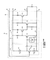
図1は、台形波出力回路の電気的構成図である。この図1に示す台形波出力回路31は、車載用のICとして構成されている。ICの高電位側の電源端子32と低電位側の電源端子33との間に電源電圧VBとしてバッテリ電圧(12V〜16V)を直接印加できるようにするため、本ICはMOSICに対し比較的高耐圧化が容易なバイポーラICとして構成されている。
【0018】
台形波出力回路31は、充放電回路34、駆動回路35およびNPN型の出力トランジスタ36などから構成されている。電源端子32、33にはそれぞれ電源線37、38が接続されている。出力トランジスタ36のコレクタは図示極性の逆電流遮断用のダイオード39を介して電源線37に接続され、エミッタは出力端子40に接続されている。出力端子40と電源端子33との間には負荷41が接続されており、負荷41に対しハイサイド側に位置する出力トランジスタ36は、負荷41に対して電流を流し出すように動作(ソース動作)する。
【0019】
上記充放電回路34において、電源線37と38との間には定電流回路42(第1の定電流回路に相当)、スイッチ回路43および定電流回路44(第2の定電流回路に相当)が直列に接続されている。定電流回路42とスイッチ回路43との共通接続点は充放電回路34の出力端子であって、当該出力端子と電源線38との間にコンデンサ45が接続されている。スイッチ回路43は、例えばアナログスイッチにより構成され、端子46を介して外部から与えられる切替信号Saに従ってオンオフ動作を行うようになっている。
【0020】
駆動回路35は、PNP型のトランジスタ47、NPN型のトランジスタ48およびPNP型トランジスタ49からなる3段構成の増幅回路である。各トランジスタ47〜49のコレクタは、直接または逆電流遮断用のダイオード50を介して電源線37または38に接続されており、全てエミッタフォロアの接続形態となっている。1段目のトランジスタ47のベースは、駆動回路35の入力端子であって、上記充放電回路34の出力端子に接続されている。また、そのエミッタは、抵抗51を介して電源線37に接続されるとともに2段目のトランジスタ48のベースに接続されている。さらに、トランジスタ48のエミッタは、抵抗52を介して電源線38に接続されるとともに3段目のトランジスタ49のベースに接続されている。トランジスタ49のエミッタは、駆動回路35の出力端子であって、抵抗53を介して電源線37に接続されるとともに上記出力トランジスタ36のベースに接続されている。
【0021】
トランジスタ48のベースと電源線38との間には、オペアンプ55を主体に構成されるクランプ回路54(電圧制限回路に相当)が接続されている。このオペアンプ55は電源線37、38から電源電圧VBを得て動作するようになっている。オペアンプ55の反転入力端子は、トランジスタ48のベースに接続されるとともに図示極性のダイオード56を介して自らの出力端子に接続され、非反転入力端子と電源線38との間には、制限電圧Vaに対応した基準電圧を生成する基準電圧発生回路57が接続されている。なお、オペアンプ55とダイオード56とからなる回路がインピーダンス回路および制御回路に相当する。
【0022】
次に、本実施形態の動作について図2および図3も参照しながら説明する。
上記構成を持つ台形波出力回路31から出力される台形波電圧は、車室内に設置されたスイッチの状態を検出するためのバイアス回路、あるいは車内LANを構築する場合の通信信号出力回路などで用いられる。
【0023】
図2は、上記バイアス回路の電気的構成を示している。スイッチ58a〜58dの各一端子は、それぞれ抵抗59a〜59dにより台形波出力回路31の出力端子40にプルアップされており、電子制御装置(ECU)内に具備されたCPU60の入力ポート60a〜60dは、それぞれ上記各一端子に接続されている。図1に示す負荷41は、これらスイッチ58a〜58dおよび抵抗59a〜59dから構成される回路を代表したものである。
【0024】
この場合、消費電流を低減するため、台形波出力回路31は、CPU60がスイッチ58a〜58dの状態を読み込む時だけ、切替信号Saに従って台形波電圧を出力するようになっている。台形波電圧は、立ち上がりおよび立ち下がりのスルーレートが小さいので誘導放射が抑えられ、矩形波電圧を用いた場合に比べラジオノイズを低減することができるためである。
【0025】
図3は、スイッチ回路43のオンオフ状態、コンデンサ45の端子電圧Vc(すなわち充放電回路34の出力電圧)の波形、出力端子40における出力電圧Voの波形および図9に示す従来構成における出力電圧Voの波形を示している。この図3において、時刻t1に切替信号SaがLレベルになると、スイッチ回路43がオフとなり、コンデンサ45の端子電圧Vcは、定電流回路42から出力される一定の電流Iaにより一定のスルーレートで上昇する。図示しないが、定電流回路42の出力部はカレントミラー回路から構成されており、端子電圧Vcは,ほぼ電源電圧VBに到達するまで上昇し、到達した時刻t3以降はその電圧VBを維持する。
【0026】
一方、時刻t4において切替信号SaがHレベルになると、スイッチ回路43がオンとなり、コンデンサ45の端子電圧Vcは、定電流回路44の電流Ibと定電流回路42の電流Iaとの差の電流(Ib−Ia)により一定のスルーレートで下降する。定電流回路44の出力部もカレントミラー回路から構成されており、端子電圧Vcはほぼ0Vに到達するまで下降し、到達した時刻t6以降はその電圧0Vを維持する。
【0027】
このコンデンサ45の端子電圧Vcは、1段目のトランジスタ47のベースに与えられ、ベース・エミッタ間電圧VBE(ダイオードの順方向電圧に等しいので以下電圧VFとして記載する)だけ高電位側にレベルシフトされて2段目のトランジスタ48のベース電圧となる。このトランジスタ48のベース電圧は、クランプ回路54によって制限電圧Va以下に制限される。本実施形態では、この制限電圧Va(基準電圧発生回路57の基準電圧)を(VB−VF)に設定している。
【0028】
ここで、コンデンサ45の端子電圧Vcが(Va−VF)よりも低い場合、トランジスタ48のベース電圧が制限電圧Vaよりも低くなる。この場合には、オペアンプ55の出力電圧がほぼ電源電圧VBとなり、ダイオード56が逆バイアスされる。この時、トランジスタ48のベースと、低インピーダンスで電流を吸い込むオペアンプ55の出力端子とは電気的に切り離された状態(遮断状態)となる。図3においては、時刻t2以前および時刻t5以降の各期間が上記遮断状態となる。
【0029】
これに対し、コンデンサ45の端子電圧Vcが(Va−VF)よりも高い場合には、トランジスタ48のベース電圧が制限電圧Vaを超えようとするため、オペアンプ55の出力電圧が低下してダイオード56が順バイアス(通電状態)となる。この時、オペアンプ55は、電源線37から抵抗51およびダイオード56を介して電流を吸い込み、この電流によってトランジスタ48のベース電圧は制限電圧Va一定に制限される。図3においては、時刻t2から時刻t5までの期間が上記通電状態となる。
【0030】
このトランジスタ48のベース電圧は、トランジスタ48および49によってそれぞれ低電位側および高電位側にVFずつレベルシフトされ、出力トランジスタ36のベース電圧となる。その結果、出力トランジスタ36のベース電圧とトランジスタ48のベース電圧とは等しくなり、出力トランジスタ36のベース電圧は、コンデンサ45の端子電圧Vcにかかわらず、制限電圧Va(=VB−VF)以下に制限される。これに伴って、そのエミッタ電圧も(Va−VF)つまり(VB−2・VF)以下に制限される。
【0031】
一方、出力トランジスタ36のコレクタ電圧は、電源電圧VBからダイオード39の順方向電圧VFだけ低下した電圧(VB−VF)となる。従って、出力トランジスタ36のコレクタ・エミッタ間電圧VCEは、以下の(1)式に示すように、コンデンサ45の端子電圧Vcにかかわらず常にVF以上となり、出力トランジスタ36は能動領域で動作するようになる。
VCE>(VB−VF)−(VB−2・VF)=VF …(1)
【0032】
その結果、出力トランジスタ36には飽和動作による少数キャリア蓄積効果が発生せず、出力トランジスタ36のエミッタ電圧つまり台形波出力回路31の出力電圧Voは、コンデンサ45の端子電圧Vcに従った歪みのない良好な台形波電圧となる。これに対し、図9に示した従来構成の台形波出力回路1の場合には、端子電圧Vcがほぼ(VB−VF)以上になると出力トランジスタ6が飽和動作となり、図3の最下段に示すように出力電圧Voの低下開始時において波形歪み(A部)が発生していた。
【0033】
以上説明したように、本実施形態によれば、駆動回路35にクランプ回路54を設けたので、出力トランジスタ36が常に能動領域で動作するようになり、台形波出力回路31は、負荷41に対して、充放電回路34において生成された台形波電圧に従った歪みの小さい電圧Voを出力することができる。これにより、従来構成の台形波出力回路1を使用した場合に比べ、図2に示すバイアス回路あるいはLANを構成する通信線(図示せず)からの誘導放射を抑制することができ、ラジオノイズをより低減することができる。
【0034】
特に、バイアス回路を備えたECU、通信線、通信信号出力回路などをラジオに接近して配置せざるを得ない車両(自動車)においては、わずかな歪みが存在しても高調波成分が増加してラジオノイズが増大するという事情がある。このため、上述した台形波出力回路31を用いることにより、ラジオノイズについて大きな低減効果が得られる。
【0035】
クランプ回路54は、駆動回路35を構成する2段目のトランジスタ48のベース電圧を制限するので、例えば出力電圧Voを直接制限する回路構成に比べ、クランプ回路54の電流吸い込み能力を比較的小さく設定することができる。その結果、チップ面積や消費電流の増加分を小さく抑えることができる。また、クランプ回路54は、コンデンサ45に対しバッファ回路として機能する1段目のトランジスタ47を介した後の電圧を制限しているので、コンデンサ45の充電電荷への影響が非常に小さくなり、出力電圧Voの歪みをより一層低減することができる。さらに、台形波出力回路31は、その充放電回路34においてコンデンサ45への充放電を定電流で行っているので、一定のスルーレートで上昇し下降する高調波成分の小さい台形波電圧を出力することが可能となる。
【0036】
(第2の実施形態)
次に、本発明を台形波出力回路に適用した第2の実施形態について、図4および図5を参照しながら説明する。なお、台形波出力回路の電気的構成を示す図4において、図1と同一構成部分には同一符号を付して示し、ここでは異なる構成部分について説明する。
【0037】
図4に示す台形波出力回路61は、図1に示す台形波出力回路31に対し、駆動回路62に設けられたクランプ回路63(電圧制限回路に相当)の構成が異なっている。すなわち、このクランプ回路63において、電源線37と38との間には図示極性のダイオード64、65と抵抗66(インピーダンス回路に相当)とが直列に接続されており、トランジスタ48のベースと電源線38との間にはPNP型のトランジスタ67のエミッタ・コレクタ間が接続されている。そして、トランジスタ67のベースは、ダイオード65と抵抗66との共通接続点に接続されている。ここで、ダイオード64、65とトランジスタ67とからなる回路部分が基準電圧発生回路および制御回路に相当する。
【0038】
この構成において、ダイオード64、65と抵抗66との直列回路には常に電流が流れており、トランジスタ67のベース電圧は(VB−2・VF)となっている。コンデンサ45の端子電圧Vcが(VB−2・VF)よりも低い場合には、トランジスタ48のベース電圧(トランジスタ67のエミッタ電圧)が制限電圧(VB−VF)よりも低くなるので、トランジスタ67のベース・エミッタ間電圧はVFよりも低くなってトランジスタ67はオフ状態となる。これに対し、コンデンサ45の端子電圧Vcが(VB−2・VF)よりも高い場合には、トランジスタ67がオン状態となり、トランジスタ48のベース電圧は制限電圧(VB−VF)一定に制限される。
【0039】
このように、本実施形態で用いるクランプ回路63は第1の実施形態で用いたクランプ回路54と同様の機能を有するので、本実施形態によっても第1の実施形態と同様の効果を得ることができる。図5は、台形波出力回路61の出力電圧波形(実測波形)とその拡大波形(a)および台形波出力回路1(図9参照)の出力電圧波形(実測波形)とその拡大波形(b)を示している。両者を比較すると、台形波出力回路61の方が出力電圧VoのA部における歪みが小さく、これに伴って負荷41に流れる出力電流の歪みも小さくなる。実測した結果では、台形波出力回路1に替えて台形波出力回路61を用いることによりラジオノイズが4dBm改善された。
【0040】
さらに、本実施形態では、トランジスタ67のベース電圧が、電源線37の電圧VBから2・VFだけ低下した電圧として定まるので、トランジスタ67がオンしたクランプ動作中において、トランジスタ48のベース電圧およびトランジスタ36のベース電圧とエミッタ電圧は、電源線37の電位を基準電位として定まる。また、出力トランジスタ36のコレクタ電圧も電源線37の電位を基準として定まる。つまり、上記クランプ動作中において、出力トランジスタ36のエミッタとコレクタの電圧はともに電源電圧VBの下で定まることになり、電源電圧VBが変動しても出力トランジスタ36のコレクタ・エミッタ間電圧が変動することがなくなる。その結果、電源電圧変動にかかわらず、出力トランジスタ36を確実に能動領域で動作させることができ、出力電圧Voの歪みの発生をより確実に防止することができる。
【0041】
(第3の実施形態)
図6は、本発明の第3の実施形態である台形波出力回路68の電気的構成図で、図1と同一構成部分には同一符号を付して示している。この台形波出力回路68の駆動回路69は、クランプ回路54がトランジスタ47のベースと電源線38との間に接続されている点に特徴を有している。この場合、基準電圧発生回路57の基準電圧Vaは(VB−2・VF)に設定されている。クランプ回路54は、遮断状態における入力インピーダンスが高いので、コンデンサ45の充電電荷に及ぼす影響はほとんどない。
【0042】
クランプ回路54によって、トランジスタ47のベース電圧(コンデンサ45の端子電圧Vc)が(VB−2・VF)に制限され、トランジスタ48のベース電圧が(VB−VF)に制限されるので、本実施形態によっても第1の実施形態と同様の効果を得ることができる。また、クランプ回路54に替えて、第2の実施形態で説明したクランプ回路63を採用しても同様の作用および効果を得ることができる。
【0043】
(第4の実施形態)
図7は、本発明の第4の実施形態である台形波出力回路70の電気的構成図で、図1と同一構成部分には同一符号を付して示している。この台形波出力回路70の駆動回路71は、クランプ回路54が出力トランジスタ36のエミッタと電源線38との間に接続されている点に特徴を有している。この場合、クランプ回路54は十分な電流吸い込み能力を有するオペアンプ55を備えており、基準電圧発生回路57の基準電圧Vaは(VB−2・VF)に設定されている。また、駆動回路71は、従来構成の台形波出力回路1(図9参照)で用いられた駆動回路5と同じ構成を有する。
【0044】
こうした構成によれば、クランプ回路54が出力トランジスタ36のエミッタ電圧を(VB−2・VF)に制限し、出力トランジスタ36のコレクタ・エミッタ間電圧VCEが常にVF以上となる。従って、出力トランジスタ36が常に能動領域で動作するようになり、第1の実施形態とほぼ同様の効果を得ることができる。なお、本実施形態においても、クランプ回路54に替えてクランプ回路63を採用することができる。
【0045】
(第5の実施形態)
上述の第1ないし第4の実施形態では駆動回路を3段のエミッタフォロア回路により構成したが、駆動回路の段数はこの限りでない。図8は、本発明の第5の実施形態である台形波出力回路72の電気的構成図であって、図4と同一構成部分には同一符号を付して示している。この図8において、駆動回路73は、トランジスタ47からなる1段のエミッタフォロア回路により構成されている。電源線37と38との間にはクランプ回路63が接続されており、そのトランジスタ67のエミッタは、出力トランジスタ36のベースに接続されている。
【0046】
本実施形態の台形波出力回路72によっても、出力トランジスタ36のベース電圧は(VB−VF)に制限されるので、第2の実施形態で述べた台形波出力回路61と同様の効果を得ることができる。なお、クランプ回路63に替えて、クランプ回路54を採用しても同様の作用および効果を得ることができる。
【0047】
(その他の実施形態)
なお、本発明は上記し且つ図面に示す各実施形態に限定されるものではなく、例えば以下のように変形または拡張が可能である。
各駆動回路の増幅段数は1または3に限られず、2あるいは4以上であっても良い。また、各駆動回路は、エミッタフォロア回路に限定されず、他の回路構成であっても良い。さらに、抵抗52、53に替えてそれぞれ定電流回路を用いても良い。
【0048】
各実施形態では、出力トランジスタ36のベース電圧が(VB−VF)に制限されるようにクランプ回路54、63の制限電圧を設定したが、出力トランジスタ36が飽和領域での動作とならない範囲内において制限電圧を他の値に設定しても良い。
第5の実施形態において、クランプ回路63(または54)を、トランジスタ47のベースと電源線38との間または出力トランジスタ36のエミッタと電源線38との間に接続しても良い。
【0049】
各台形波出力回路において、電源線37、38に対する接続形態を逆にし、且つ各トランジスタのタイプをPNP型とNPN型との間で替えることにより、PNP型の出力トランジスタが負荷41に対しロウサイド側に位置するように構成しても良い。この場合、出力トランジスタは、電流吸い込み動作(シンク動作)となる。
【図面の簡単な説明】
【図1】本発明の第1の実施形態を示す台形波出力回路の電気的構成図
【図2】スイッチ状態を検出するためのバイアス回路の電気的構成図
【図3】台形波電圧を生成する場合における各部の電圧波形を示す図
【図4】本発明の第2の実施形態を示す図1相当図
【図5】(a)台形波出力回路61の出力電圧波形とその拡大波形を示す図、および(b)台形波出力回路1の出力電圧波形とその拡大波形を示す図
【図6】本発明の第3の実施形態を示す図1相当図
【図7】本発明の第4の実施形態を示す図1相当図
【図8】本発明の第5の実施形態を示す図1相当図
【図9】従来構成を示す図1相当図
【符号の説明】
31、61、68、70、72は台形波出力回路、34は充放電回路、35、62、69、71、73は駆動回路、36は出力トランジスタ、37、38は電源線、41は負荷、42は定電流回路(第1の定電流回路)、44は定電流回路(第2の定電流回路)、45はコンデンサ、54、63はクランプ回路(電圧制限回路)、57は基準電圧発生回路である。[0001]
BACKGROUND OF THE INVENTION
The present invention relates to a trapezoidal wave output circuit that outputs a trapezoidal waveform voltage corresponding to a charging voltage of a capacitor to a load.
[0002]
[Prior art]
For example, an in-vehicle communication signal output circuit outputs a trapezoidal signal having a small rising and falling slew rate in order to reduce radio noise by suppressing stimulated emission from a communication line disposed in a vehicle. It is like that. Examples of such trapezoidal wave output circuits include circuits disclosed in Japanese Patent Laid-Open Nos. 6-214665 and 9-261016. These circuits are configured to generate a trapezoidal wave signal by charging and discharging a capacitor with a constant current.
[0003]
[Problems to be solved by the invention]
FIG. 9 shows an electrical configuration of a general trapezoidal wave output circuit of this type. In FIG. 9, the trapezoidal wave output circuit 1 formed as an IC operates with a relatively high power supply voltage VB (for example, a voltage of 12V to 16V output from the battery) applied between the
[0004]
The trapezoidal wave output circuit 1 includes a charge / discharge circuit 4, a drive circuit 5, and an output transistor 6, and a
[0005]
In this configuration, a trapezoidal voltage is generated between both terminals of the capacitor 9 based on the switching signal Sa, and this voltage becomes the base voltage of the output transistor 6 while being sequentially level-shifted by the
[0006]
Now, when the switch circuit 13 is off, the capacitor 9 is charged by the constant
[0007]
Thereafter, when the switch 13 is turned on and discharging of the capacitor 9 is started, the terminal voltage Vc starts to decrease, and accordingly, the base voltage of the output transistor 6 also starts to decrease from the power supply voltage VB. However, since the output transistor 6 has been operating in the saturation region until then, a minority carrier accumulation effect occurs, and a phenomenon occurs in which the emitter voltage does not decrease during the saturation recovery time even if the base voltage decreases. As a result, the trapezoidal output voltage Vo has a waveform distortion at the falling start point, and there is a problem that radio noise increases due to an increase in harmonic components due to the distortion.
[0008]
The present invention has been made in view of the above circumstances, and an object thereof is to provide a trapezoidal wave output circuit in which distortion of output voltage is reduced.
[0009]
[Means for Solving the Problems]
According to the means described in claim 1, the charging / discharging circuit generates a trapezoidal charging voltage by charging / discharging the capacitor, and the driving circuit drives the output transistor based on this charging voltage. Thereby, the output transistor outputs a trapezoidal voltage corresponding to the charging voltage of the capacitor to the load. In this case, the voltage limiting circuit provided in the driving circuit limits the voltage of any node to which the charging voltage is transmitted in the driving circuit, so that the output transistor operates in the active region. Limit (base terminal voltage).
[0010]
As a result, the generation of the minority carrier accumulation effect in the output transistor is prevented, and the output transistor can output a trapezoidal wave voltage corresponding to the charging voltage of the capacitor without distortion. For example, if this trapezoidal wave voltage is used for a bias circuit for detecting the state of a switch installed in a vehicle interior of a vehicle or a communication signal output circuit for constructing an in-vehicle LAN, induced radiation is suppressed and radio noise is reduced.
[0011]
According to the means described in
[0012]
According to the third aspect of the present invention, since the drive circuit is composed of the emitter follower circuit, the base terminal and emitter terminal of each transistor (in the case of a multi-stage configuration, it is also the base terminal of the next-stage transistor). The voltage is a voltage equal to the terminal voltage of the capacitor or a voltage level-shifted by a constant voltage. In this case, the voltage at the base terminal of the output transistor can be limited by limiting the voltage at either the base terminal or the emitter terminal of each transistor. However, in this means, the voltage at the base terminal is particularly limited. Thus, the current sink (or discharge) capability of the voltage limiting circuit can be set relatively small. Further, since the emitter follower circuit has a high input impedance, the influence of the drive circuit on the charge of the capacitor is reduced, and the distortion of the charge voltage of the capacitor and hence the output voltage is further reduced.
[0013]
According to the means described in claim 4, the operation state (saturation operation or active operation) of the output transistor is level-shifted by a constant voltage (base-emitter voltage VBE) from the voltage of the base terminal supplied from the drive circuit. It is determined based on the voltage of the emitter terminal and the voltage of the collector terminal connected to one power supply line (directly or via an element such as a diode). On the other hand, the voltage limiting circuit is configured to limit the voltage using the one power line as a reference potential. As a result, the voltage at the emitter terminal and the collector terminal of the output transistor is determined under the same reference potential, and even if the power supply voltage fluctuates during the voltage limiting operation by the voltage limiting circuit, the collector-emitter voltage of the output transistor Will not fluctuate. Therefore, the output transistor can be reliably operated in the active region regardless of the power supply voltage fluctuation.
[0014]
According to the means described in claim 5, as in the means described in claim 1, the output transistor outputs a trapezoidal voltage corresponding to the charging voltage of the capacitor to the load. In this case, since the voltage limiting circuit limits the output voltage (voltage across the load) so that the output transistor operates in the active region, the generation of the minority carrier accumulation effect in the output transistor is prevented. It is possible to output a trapezoidal wave voltage corresponding to the charging voltage without distortion. Thereby, the radio noise can be reduced in the same manner as the means described in claim 1.
[0015]
According to the means described in claim 6, when the voltage of the node that limits the voltage exceeds the reference voltage corresponding to the limit voltage, a current flows from the node to the impedance circuit (or vice versa), and the voltage generated by this current Due to the drop, the voltage of the node is held at the limit voltage.
[0016]
According to the means described in claim 7, since the charging / discharging circuit includes the first and second constant current circuits for charging / discharging the capacitor, charging / discharging with a constant current is possible, It becomes possible to generate a trapezoidal voltage with a small harmonic component that rises and falls at a constant slew rate.
According to the means described in
According to the means described in claim 9, the charge / discharge circuit and the drive circuit are connected between the pair of power supply lines, and the drive circuit receives the terminal voltage of the capacitor as an input and is in a single stage or a multistage form in the form of an emitter follower. The collector of the transistor is connected to either one of a pair of power supply lines directly or via a reverse current blocking diode.
[0017]
DETAILED DESCRIPTION OF THE INVENTION
(First embodiment)
Hereinafter, a first embodiment of the present invention will be described with reference to FIGS. 1 to 3.
FIG. 1 is an electrical configuration diagram of a trapezoidal wave output circuit. The trapezoidal
[0018]
The trapezoidal
[0019]
In the charge /
[0020]
The
[0021]
A clamp circuit 54 (corresponding to a voltage limiting circuit) mainly composed of an
[0022]
Next, the operation of the present embodiment will be described with reference to FIGS.
The trapezoidal wave voltage output from the trapezoidal
[0023]
FIG. 2 shows the electrical configuration of the bias circuit. Each one terminal of the
[0024]
In this case, in order to reduce current consumption, the trapezoidal
[0025]
3 shows the ON / OFF state of the
[0026]
On the other hand, when the switching signal Sa becomes H level at the time t4, the
[0027]
The terminal voltage Vc of the
[0028]
Here, when the terminal voltage Vc of the
[0029]
On the other hand, when the terminal voltage Vc of the
[0030]
The base voltage of the
[0031]
On the other hand, the collector voltage of the
VCE> (VB−VF) − (VB−2 · VF) = VF (1)
[0032]
As a result, a minority carrier accumulation effect due to the saturation operation does not occur in the
[0033]
As described above, according to the present embodiment, since the
[0034]
In particular, in a vehicle (automobile) in which an ECU having a bias circuit, a communication line, a communication signal output circuit, etc. must be arranged close to the radio, harmonic components increase even if slight distortion exists. As a result, radio noise increases. For this reason, the use of the trapezoidal
[0035]
Since the
[0036]
(Second Embodiment)
Next, a second embodiment in which the present invention is applied to a trapezoidal wave output circuit will be described with reference to FIGS. In FIG. 4 showing the electrical configuration of the trapezoidal wave output circuit, the same components as those in FIG. 1 are denoted by the same reference numerals, and different components will be described here.
[0037]
The trapezoidal
[0038]
In this configuration, a current always flows through the series circuit of the diodes 64 and 65 and the
[0039]
As described above, since the
[0040]
Furthermore, in this embodiment, the base voltage of the
[0041]
(Third embodiment)
FIG. 6 is an electrical configuration diagram of a trapezoidal
[0042]
The
[0043]
(Fourth embodiment)
FIG. 7 is an electrical configuration diagram of a trapezoidal wave output circuit 70 according to the fourth embodiment of the present invention, and the same components as those in FIG. The drive circuit 71 of the trapezoidal wave output circuit 70 is characterized in that the
[0044]
According to such a configuration, the
[0045]
(Fifth embodiment)
In the first to fourth embodiments described above, the drive circuit is configured by a three-stage emitter follower circuit, but the number of stages of the drive circuit is not limited to this. FIG. 8 is an electrical configuration diagram of the trapezoidal
[0046]
Also by the trapezoidal
[0047]
(Other embodiments)
The present invention is not limited to the embodiments described above and shown in the drawings, and can be modified or expanded as follows, for example.
The number of amplification stages of each drive circuit is not limited to 1 or 3, and may be 2 or 4 or more. Each drive circuit is not limited to an emitter follower circuit, and may have other circuit configurations. Further, constant current circuits may be used in place of the
[0048]
In each embodiment, the limiting voltage of the
In the fifth embodiment, the clamp circuit 63 (or 54) may be connected between the base of the
[0049]
In each trapezoidal wave output circuit, the connection form to the
[Brief description of the drawings]
FIG. 1 is an electrical configuration diagram of a trapezoidal wave output circuit showing a first embodiment of the present invention.
FIG. 2 is an electrical configuration diagram of a bias circuit for detecting a switch state.
FIG. 3 is a diagram showing voltage waveforms at various parts when generating a trapezoidal wave voltage;
FIG. 4 is a view corresponding to FIG. 1, showing a second embodiment of the present invention.
5A is a diagram showing an output voltage waveform of a trapezoidal
FIG. 6 is a view corresponding to FIG. 1, showing a third embodiment of the present invention.
FIG. 7 is a view corresponding to FIG. 1, showing a fourth embodiment of the present invention.
FIG. 8 is a view corresponding to FIG. 1, showing a fifth embodiment of the present invention.
9 is a view corresponding to FIG. 1 showing a conventional configuration.
[Explanation of symbols]
31, 61, 68, 70 and 72 are trapezoidal wave output circuits, 34 is a charge / discharge circuit, 35, 62, 69, 71 and 73 are drive circuits, 36 is an output transistor, 37 and 38 are power lines, 41 is a load, 42 is a constant current circuit (first constant current circuit), 44 is a constant current circuit (second constant current circuit), 45 is a capacitor, 54 and 63 are clamp circuits (voltage limiting circuits), and 57 is a reference voltage generating circuit. It is.
Claims (9)
負荷に対して直列に接続された出力トランジスタと、
この出力トランジスタが前記負荷に対して前記コンデンサの充電電圧に応じた台形波状の電圧を出力するように、前記コンデンサの充電電圧に基づいて前記出力トランジスタを駆動する駆動回路とを備え、
前記駆動回路は、前記コンデンサの充電電圧にかかわらず前記出力トランジスタが常に能動領域で動作するように、前記出力トランジスタの駆動電圧を制限する電圧制限回路を備えて構成されていることを特徴とする台形波出力回路。A charge / discharge circuit having a capacitor for charging / discharging the capacitor;
An output transistor connected in series with the load;
A drive circuit for driving the output transistor based on the charging voltage of the capacitor, so that the output transistor outputs a trapezoidal voltage corresponding to the charging voltage of the capacitor to the load;
The drive circuit includes a voltage limiting circuit that limits the drive voltage of the output transistor so that the output transistor always operates in an active region regardless of the charging voltage of the capacitor. Trapezoidal wave output circuit.
前記電圧制限回路は、前記トランジスタまたは前記出力トランジスタのベース端子の電圧を制限するように構成されていることを特徴とする請求項1記載の台形波出力回路。The drive circuit is composed of one or a plurality of transistors connected in a single stage or multiple stages in the form of an emitter follower with the terminal voltage of the capacitor as an input,
The trapezoidal wave output circuit according to claim 1, wherein the voltage limiting circuit is configured to limit a voltage at a base terminal of the transistor or the output transistor.
前記出力トランジスタは、前記電源線間において一電源線と前記負荷との間に接続されているとともに、前記電圧制限回路は、前記一電源線を基準電位として電圧を制限するように構成されていることを特徴とする請求項1ないし3の何れかに記載の台形波出力回路。The charge / discharge circuit and the drive circuit are connected between a pair of power supply lines,
The output transistor is connected between the power supply line between one power supply line and the load, and the voltage limiting circuit is configured to limit the voltage using the one power supply line as a reference potential. The trapezoidal wave output circuit according to claim 1, wherein the trapezoidal wave output circuit is provided.
負荷に対して直列に接続された出力トランジスタと、
この出力トランジスタが前記負荷に対して前記コンデンサの充電電圧に応じた台形波状の電圧を出力するように、前記コンデンサの充電電圧に基づいて前記出力トランジスタを駆動する駆動回路と、
前記コンデンサの充電電圧にかかわらず前記出力トランジスタが常に能動領域で動作するように、前記出力トランジスタの出力電圧を制限する電圧制限回路とを備えて構成されていることを特徴とする台形波出力回路。A charge / discharge circuit having a capacitor for charging / discharging the capacitor;
An output transistor connected in series with the load;
A drive circuit for driving the output transistor based on the charge voltage of the capacitor, so that the output transistor outputs a trapezoidal voltage corresponding to the charge voltage of the capacitor to the load;
A trapezoidal wave output circuit comprising a voltage limiting circuit for limiting the output voltage of the output transistor so that the output transistor always operates in an active region regardless of the charging voltage of the capacitor. .
インピーダンス回路と、
制限電圧に対応した基準電圧を生成する基準電圧発生回路と、
電圧を制限するノードの電圧が前記基準電圧を超える場合に、前記ノードと前記インピーダンス回路とを電気的に接続する制御回路とから構成されていることを特徴とする請求項1ないし5の何れかに記載の台形波出力回路。The voltage limiting circuit is:
An impedance circuit;
A reference voltage generation circuit for generating a reference voltage corresponding to the limit voltage;
6. The control circuit according to claim 1, further comprising a control circuit that electrically connects the node and the impedance circuit when a voltage of a node that limits a voltage exceeds the reference voltage. The trapezoidal wave output circuit described in 1.
前記出力トランジスタのコレクタは、逆電流遮断用のダイオードを介して前記一電源線に接続されていることを特徴とする請求項1ないし7の何れかに記載の台形波出力回路。The trapezoidal wave output circuit according to any one of claims 1 to 7, wherein a collector of the output transistor is connected to the one power supply line via a diode for blocking a reverse current.
前記駆動回路は、前記コンデンサの端子電圧を入力としエミッタフォロアの形態で1段または多段に接続された1または複数のトランジスタから構成され、The drive circuit is composed of one or a plurality of transistors connected in a single stage or multiple stages in the form of an emitter follower with the terminal voltage of the capacitor as an input,
前記トランジスタのコレクタは、直接または逆電流遮断用のダイオードを介して前記一対の電源線のうち何れか一方に接続されていることを特徴とする請求項1ないし8の何れかに記載の台形波出力回路。The trapezoidal wave according to any one of claims 1 to 8, wherein the collector of the transistor is connected to one of the pair of power supply lines directly or via a diode for blocking a reverse current. Output circuit.
Priority Applications (1)
| Application Number | Priority Date | Filing Date | Title |
|---|---|---|---|
| JP2000335598A JP4622085B2 (en) | 2000-11-02 | 2000-11-02 | Trapezoidal wave output circuit |
Applications Claiming Priority (1)
| Application Number | Priority Date | Filing Date | Title |
|---|---|---|---|
| JP2000335598A JP4622085B2 (en) | 2000-11-02 | 2000-11-02 | Trapezoidal wave output circuit |
Publications (2)
| Publication Number | Publication Date |
|---|---|
| JP2002141782A JP2002141782A (en) | 2002-05-17 |
| JP4622085B2 true JP4622085B2 (en) | 2011-02-02 |
Family
ID=18811313
Family Applications (1)
| Application Number | Title | Priority Date | Filing Date |
|---|---|---|---|
| JP2000335598A Expired - Fee Related JP4622085B2 (en) | 2000-11-02 | 2000-11-02 | Trapezoidal wave output circuit |
Country Status (1)
| Country | Link |
|---|---|
| JP (1) | JP4622085B2 (en) |
Families Citing this family (1)
| Publication number | Priority date | Publication date | Assignee | Title |
|---|---|---|---|---|
| JP2007013916A (en) * | 2005-05-30 | 2007-01-18 | Denso Corp | Signal generator |
Citations (1)
| Publication number | Priority date | Publication date | Assignee | Title |
|---|---|---|---|---|
| JP2000138570A (en) * | 1998-08-28 | 2000-05-16 | Denso Corp | Electric load driver |
Family Cites Families (8)
| Publication number | Priority date | Publication date | Assignee | Title |
|---|---|---|---|---|
| JPS63296023A (en) * | 1987-05-28 | 1988-12-02 | Sony Corp | Liquid crystal display device |
| JPH06164262A (en) * | 1992-11-25 | 1994-06-10 | Nec Ic Microcomput Syst Ltd | Saturation prevention circuit |
| JPH0786895A (en) * | 1993-09-16 | 1995-03-31 | Toshiba Corp | Output circuit |
| JPH09105763A (en) * | 1995-10-11 | 1997-04-22 | Nec Corp | Comparator circuit |
| JP3603457B2 (en) * | 1996-03-19 | 2004-12-22 | 株式会社デンソー | Trapezoidal wave signal output device |
| JP3747591B2 (en) * | 1997-10-03 | 2006-02-22 | ソニー株式会社 | Semiconductor circuit |
| JP2000022506A (en) * | 1998-07-07 | 2000-01-21 | Mitsubishi Heavy Ind Ltd | Noninverted amplifier circuit provided with trapezoidal waveform output function |
| JP3654149B2 (en) * | 2000-07-04 | 2005-06-02 | 株式会社デンソー | Data communication device |
-
2000
- 2000-11-02 JP JP2000335598A patent/JP4622085B2/en not_active Expired - Fee Related
Patent Citations (1)
| Publication number | Priority date | Publication date | Assignee | Title |
|---|---|---|---|---|
| JP2000138570A (en) * | 1998-08-28 | 2000-05-16 | Denso Corp | Electric load driver |
Also Published As
| Publication number | Publication date |
|---|---|
| JP2002141782A (en) | 2002-05-17 |
Similar Documents
| Publication | Publication Date | Title |
|---|---|---|
| JPH0317713A (en) | Power-transistor driver circuit having improved short-circuit protective function | |
| JP2006311419A (en) | Signal output circuit | |
| JP3920371B2 (en) | Charging device, current detection circuit, and voltage detection circuit | |
| WO2021124644A1 (en) | Gate drive circuit | |
| JPH07235868A (en) | Current buffer circuit | |
| JP4622085B2 (en) | Trapezoidal wave output circuit | |
| JP3608472B2 (en) | Output circuit | |
| US6046623A (en) | Signal detecting circuit | |
| JP3711860B2 (en) | Output circuit | |
| JP3620766B2 (en) | Voltage supply circuit for amplifier | |
| US6850111B1 (en) | Charge pump circuit | |
| US4764688A (en) | Output current darlington transistor driver circuit | |
| JP2540759B2 (en) | Transistor amplifier | |
| JP2564054Y2 (en) | Switching power supply | |
| JPH1079652A (en) | Hysteresis comparator | |
| JP3671796B2 (en) | Drive device for current control element | |
| US6459249B2 (en) | Reset circuit | |
| JP3724690B2 (en) | Switching circuit | |
| JP3084470B2 (en) | Power transistor switching circuit | |
| JP3624541B2 (en) | Driver circuit | |
| JP5040853B2 (en) | Triangular wave generation circuit and voltage-pulse conversion circuit | |
| JP2001085627A (en) | Switching power supply | |
| JP2002100969A (en) | Switching circuit | |
| JP2010051102A (en) | Rush current suppressing circuit | |
| JP2000165218A (en) | Load short circuit protective circuit for proximity switch |
Legal Events
| Date | Code | Title | Description |
|---|---|---|---|
| A621 | Written request for application examination |
Free format text: JAPANESE INTERMEDIATE CODE: A621 Effective date: 20070709 |
|
| A977 | Report on retrieval |
Free format text: JAPANESE INTERMEDIATE CODE: A971007 Effective date: 20100216 |
|
| A131 | Notification of reasons for refusal |
Free format text: JAPANESE INTERMEDIATE CODE: A131 Effective date: 20100223 |
|
| A521 | Written amendment |
Free format text: JAPANESE INTERMEDIATE CODE: A523 Effective date: 20100415 |
|
| TRDD | Decision of grant or rejection written | ||
| A01 | Written decision to grant a patent or to grant a registration (utility model) |
Free format text: JAPANESE INTERMEDIATE CODE: A01 Effective date: 20101005 |
|
| A01 | Written decision to grant a patent or to grant a registration (utility model) |
Free format text: JAPANESE INTERMEDIATE CODE: A01 |
|
| A61 | First payment of annual fees (during grant procedure) |
Free format text: JAPANESE INTERMEDIATE CODE: A61 Effective date: 20101018 |
|
| FPAY | Renewal fee payment (event date is renewal date of database) |
Free format text: PAYMENT UNTIL: 20131112 Year of fee payment: 3 |
|
| R250 | Receipt of annual fees |
Free format text: JAPANESE INTERMEDIATE CODE: R250 |
|
| R250 | Receipt of annual fees |
Free format text: JAPANESE INTERMEDIATE CODE: R250 |
|
| LAPS | Cancellation because of no payment of annual fees |