JP4615397B2 - Coin image detector - Google Patents
Coin image detector Download PDFInfo
- Publication number
- JP4615397B2 JP4615397B2 JP2005243670A JP2005243670A JP4615397B2 JP 4615397 B2 JP4615397 B2 JP 4615397B2 JP 2005243670 A JP2005243670 A JP 2005243670A JP 2005243670 A JP2005243670 A JP 2005243670A JP 4615397 B2 JP4615397 B2 JP 4615397B2
- Authority
- JP
- Japan
- Prior art keywords
- coin
- light
- image
- light emitting
- time
- Prior art date
- Legal status (The legal status is an assumption and is not a legal conclusion. Google has not performed a legal analysis and makes no representation as to the accuracy of the status listed.)
- Expired - Fee Related
Links
Images


Landscapes
- Testing Of Coins (AREA)
- Image Input (AREA)
Description
本発明は、識別を行うために硬貨の画像を検出する硬貨画像検出装置に関する。 The present invention relates to a coin image detection apparatus that detects an image of a coin for identification.
識別を行うために硬貨の画像を検出する硬貨画像検出装置に関する技術として、硬貨を囲むように円環状に配置されて硬貨の表面に光を照射する複数のLEDと、これら複数のLEDで光が照射された硬貨の画像を検出するCCDエリアセンサとを有するものがある(例えば、特許文献1参照)。
ところで、上記のような硬貨画像検出装置で硬貨を検出する場合、硬貨は材質により光の反射率が高いもの(500円硬貨、100円硬貨、50円硬貨および1円硬貨)と、反射率の低いもの(10円硬貨および5円硬貨)とがあり、例えば、低反射率の硬貨にLEDの発光量を合わせると、高反射率の硬貨の画像が明るくなり過ぎてしまう。そのため、その後に行われる硬貨の真偽および金種の識別が良好にできない可能性があった。 By the way, when a coin is detected by the above-described coin image detection device, the coin has a high light reflectivity depending on the material (500 yen coin, 100 yen coin, 50 yen coin and 1 yen coin), and the reflectivity. Some of them are low (10-yen coins and 5-yen coins). For example, when the amount of light emitted from the LED is adjusted to a low-reflectance coin, the image of the high-reflectance coin becomes too bright. For this reason, there is a possibility that the authenticity of coins and the denomination of the denominations performed thereafter cannot be improved.
したがって、本発明は、硬貨の識別のための画像データを良好に検出することができる硬貨画像検出装置の提供を目的とする。 Therefore, an object of this invention is to provide the coin image detection apparatus which can detect the image data for the coin identification favorably.
上記目的を達成するために、請求項1に係る発明は、硬貨を囲むように円環状に配置されて硬貨の表面に光を照射する光照射手段と、該光照射手段で光が照射された硬貨の画像を検出する画像検出手段とを有する硬貨画像検出装置において、前記光照射手段を複数の領域に分割し、各領域毎に異なる照射タイミングで光を硬貨に照射するとともに、各照射タイミングそれぞれについて前記画像検出手段により画像を検出することを特徴としている。
In order to achieve the above-mentioned object, the invention according to
請求項1に係る発明によれば、硬貨を囲むように円環状に配置されて硬貨の表面に光を照射する光照射手段を複数の領域に分割し、各領域毎に異なる照射タイミングで光を硬貨に照射すると、各領域から偏って照射された光で硬貨には表面の凹凸による陰影が生じることになり、このような陰影を含む画像を各照射タイミングそれぞれについて画像検出手段で検出することになる。これにより、例え光照射手段の発光量を低反射率の硬貨に合わせても、高反射率の硬貨にも陰影を明確に形成することができるため、硬貨の識別のための画像データを良好に検出することができる。 According to the first aspect of the present invention, the light irradiation means arranged in an annular shape so as to surround the coin and irradiating light on the surface of the coin is divided into a plurality of regions, and light is emitted at different irradiation timings for each region. When the coins are irradiated, the coins will be shaded by the unevenness of the surface due to the light radiated from each region, and the images including such shadows will be detected by the image detection means for each irradiation timing. Become. As a result, even if the amount of light emitted from the light irradiating means is matched to a low-reflectance coin, a shadow can be clearly formed on the high-reflectance coin, so that the image data for identifying the coin can be improved. Can be detected.
本発明に係る一実施形態の硬貨画像検出装置を図面を参照して以下に説明する。
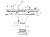
図1は、本実施形態の硬貨画像検出装置の平面図であり、図2はその側面図である。図1および図2において、硬貨1は、エンドレスベルト2により、硬貨通路3の表面に押圧されつつ、一対のガイドレール4,5に沿って、矢印Fの方向に、硬貨通路3内を送られる。硬貨通路3には、光が透過可能なガラス、アクリル樹脂などからなる透明材料により形成された透明通路部6が設けられている。硬貨1の搬送方向に対して、透明通路部6の上流側には、硬貨1の磁気的性質を検出する一対の磁気センサ7,7が設けられている。
A coin image detection device according to an embodiment of the present invention will be described below with reference to the drawings.
FIG. 1 is a plan view of the coin image detection apparatus of the present embodiment, and FIG. 2 is a side view thereof. 1 and 2, a
上記目的を達成するために、請求項1に係る発明は、硬貨を囲むように円環状に配置され該円環の全体に等間隔で配置された発光素子で構成されて硬貨の表面に光を照射する光照射手段と、該光照射手段で光が照射された硬貨の画像を検出する画像検出手段とを有する硬貨画像検出装置において、前記光照射手段は、それぞれが複数の連続配置された前記発光素子のみからなる三つの均等な領域に分割され、すべての前記領域が硬貨の移動方向に対し左右非対称であって異なる照射タイミングで光を照射可能であるとともに、すべての前記領域が一斉に光を照射可能であり、前記光照射手段のすべての前記領域が一斉に光を硬貨に照射した状態で前記画像検出手段により硬貨の全体画像を検出し、前記光照射手段を前記三つの領域に分割し、すべての前記領域が異なる照射タイミングで光を硬貨に照射するとともに、各照射タイミングそれぞれについて前記画像検出手段により画像を検出し、これら各照射タイミングそれぞれの画像を組み合わせて硬貨全体の一つの影の画像データを得て、前記全体画像から判定された、硬貨位置の確定情報、回転角の特定情報および金種・表裏の判定情報に基づいて、基準データメモリからマスタデータを読み出すとともに該マスタデータと前記影の画像データとを比較して硬貨の識別を行うことを特徴としている。
In order to achieve the above object, the invention according to
光照射部8は、図1に示すように、透明通路部6の中心部を中心とした円上に等間隔で配置された多数(例えば24個)のLEDなどの発光素子L1〜L24を備えている。各発光素子L1〜L24は、光軸が、水平方向に対して、小さな角度をなし、透明通路部6の中心部を中心とした円の中心軸上の所定の点を向くように配置されており、透明通路部6上を通過する硬貨1の表面(下面)に浅い角度で光を照射可能なようになっている。つまり、光照射部8は、透明通路部6上を通過する硬貨1を全周にわたって囲むように円環状に配置されていて、透明通路部6上を通過する硬貨1の表面(下面)に下側から光を照射する。また、円環状の光照射部8は、その中心軸線が透明通路部6上の硬貨1の中心軸線と平行または一致するように配置されている。
As shown in FIG. 1, the
画像検出部9は、光軸が、透明通路部6の中心部を中心とした円環状の光照射部8の中心軸と一致するように配置されたレンズ系構成部15と、レンズ系構成部15の下方に設けられ、その焦点が、透明通路部6の上表面に位置するように配置されており、光照射部8から発せられ、硬貨1の表面(下面)により反射された光を光電的に検出するCCD等の多数の受光素子が面状に並べられたエリアセンサ16と、エリアセンサ16により、光電的に検出されて得られた硬貨1の画像データをディジタル信号に変換して、硬貨1のディジタル化された画像データを生成する図3に示すA/Dコンバータ17とを備えている。
The
透明通路部6における画像検出部9の直下流側には、透明通路部6を介して上下に配置される発光素子18と受光素子19とからなる二組のタイミングセンサ20,20が設けられている。これらタイミングセンサ20,20は、発光素子18から発せられた光が透明通路部6を介して受光素子19により受光可能に、かつ、受光素子19が発光素子18から発せられた光を受光しないときにタイミング信号を出力するように構成されている。各タイミングセンサ20,20は、発光素子18から発せられた光が、透明通路部6の表面上を搬送される硬貨1によって遮られて受光素子19に受光されず、タイミング信号が出力されるときに、硬貨1が透明通路部6の表面上にあって、その中心が透明通路部6の中心とほぼ合致する位置にあるように配置されている。
Two sets of
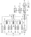
図3は、本実施形態の硬貨画像検出装置の制御系を示すブロック図である。
硬貨画像検出装置は、硬貨1が透明通路部6に達したことを検出する上記したタイミングセンサ20,20と、タイミングセンサ20からタイミング信号を受けたときに、光照射部8に発光信号を出力して光を発光させ、透明通路部6の上表面に位置する硬貨1に光を照射させる発光制御部25と、タイミングセンサ20からタイミング信号を受けたときに、画像検出部9のエリアセンサ16に、硬貨1の表面により反射された光の検出を開始させる取込制御部26とを備えている。
FIG. 3 is a block diagram showing a control system of the coin image detection apparatus of the present embodiment.
The coin image detection device outputs the light emission signal to the
また、硬貨画像検出装置は、磁気センサ7,7で検出された硬貨1の磁気的性質を示す磁気データを記憶する磁気データメモリ28と、エリアセンサ16により光電的に検出されA/Dコンバータ17によってディジタル化された硬貨1の画像パターンデータを記憶する画像データメモリ29と、磁気データの各金種毎のマスタデータおよび画像パターンデータの各金種毎のマスタデータが記憶された基準データメモリ30と、磁気センサ7,7で検出され磁気データメモリ28に記憶された硬貨1の磁気データと、基準データメモリ30に記憶されている磁気データのマスタデータとを比較するとともに、エリアセンサ16により検出され画像データメモリ29に記憶された硬貨1の画像パターンデータと、基準データメモリ30に記憶されている画像パターンデータのマスタデータとを比較して硬貨1の金種を識別する識別部31とを有している。
Further, the coin image detection apparatus is a photoelectric sensor that is detected by the
そして、本実施形態の硬貨画像検出装置では、上記した光照射部8が、図1に示すように、連続配置される複数(例えば8個)の発光素子からなる複数(例えば3つ)の円弧状の第1発光領域A1、第2発光領域A2及び第3発光領域A3に等分割されており、第1発光領域A1を構成する複数の発光素子L1〜L8が、図3に示すように、これらを同時に駆動可能な第1発光駆動部D1に接続され、第2発光領域A2を構成する複数の発光素子L9〜L16が、これらを同時に駆動可能な第2発光駆動部D2に接続され、第3発光領域A3を構成する複数の発光素子L17〜L24が、これらを同時に駆動可能な第3発光駆動部D3に接続されている。そして、発光制御部25は、第1発光領域A1、第2発光領域A2及び第3発光領域A3の各領域毎に異なる照射タイミングで光を硬貨1に向け照射することになり、取込制御部26が、各照射タイミングそれぞれについて画像検出部9のエリアセンサ16により画像を検出させる。
And in the coin image detection apparatus of this embodiment, as above-mentioned
以上のような構成の本実施形態の硬貨画像検出装置では、一の硬貨1が、エンドレスベルト2によって、硬貨通路3の表面に押圧されつつ、一対のガイドレール4,5に沿って硬貨通路3内を送られると、まず、磁気センサ7によってこの硬貨1の磁気データを検出して磁気データメモリ28に記憶させる。
In the coin image detection device of the present embodiment configured as described above, one
次に、前記一の硬貨1がタイミングセンサ20で検出されてタイミングセンサ20から図4(a)に示すように出力があった時点(図4におけるt1時点)で、発光制御部25が、図4(b)に示すように第1発光駆動部D1に第1発光駆動出力信号を、図4(c)に示すように第2発光駆動部D2に第2発光駆動出力信号を、図4(d)に示すように第3発光駆動部D3に第3発光駆動出力信号を、同時に出力し、第1発光駆動部D1、第2発光駆動部D2および第3発光駆動部D3によって第1発光領域A1、第2発光領域A2および第3発光領域A3にあるすべての発光素子L1〜L24を同時に予め調整された一定の発光時間tcだけ駆動して円環状に配置された全発光素子L1〜L24を一斉に発光時間tcだけ発光させる(図4におけるt1時点〜t2時点:tc=t2−t1)とともに、これに同期して取込制御部26が、図4(e)に示すようにエリアセンサ16に画像を取り込ませるための画像取込信号を出力して前記一の硬貨1からの反射光つまりこの硬貨1の表面(下面)の画像データをエリアセンサ16に検出させる(図4におけるt1時点〜t2時点)。そして、画像取込信号の終了時点(図4におけるt2時点)からは、図4(f)に示すように、取り込んだ画像データをA/Dコンバータ17でA/D変換して画像データメモリ29に記憶させる(図4におけるt2時点〜t4時点)。このとき、画像データを画像データメモリ29に記憶させる記憶時間tf(tf=t4−t2)は、エリアセンサ16の能力に応じて設定されることになるが、この記憶時間tfは発光時間tcより短くなるように設定されている。
Next, at the time when the one
以上によって、エリアセンサ16は、全発光素子L1〜L24の発光時の前記一の硬貨1の全体の画像データ(以下、全体画像データと称す)を検出することになり、この全体画像データを画像データメモリ29が記憶することになる。なお、エリアセンサ16は画像の検出を開始しようとする際のt1時点ですべての受光素子群が一旦クリアされる。
As described above, the
上記した画像データのエリアセンサ16による検出後(図4におけるt2時点)、必要に応じてエリアセンサ16の受光素子群からデータ移送用の素子群にデータを転送するのに必要な若干の待機時間の経過を待った後(図4におけるt3時点)、発光制御部25が、図4(b)に示すように第1発光駆動部D1のみに第1発光駆動出力信号を出力し、第1発光駆動部D1によって第1発光領域A1のみにあるすべての発光素子L1〜L8を同時に予め調整された一定の発光時間tcだけ駆動して円弧状に配置された第1発光領域A1のみの発光素子L1〜L8を一斉に発光時間tcだけ発光させる(図4におけるt3時点〜t5時点:tc=t5−t3)とともに、これに同期して取込制御部26が、図4(e)に示すようにエリアセンサ16に画像取込信号を出力して前記一の硬貨1からの反射光つまりこの硬貨1の表面(下面)の画像データをエリアセンサ16に検出させる(図4におけるt3時点〜t5時点)。そして、画像取込信号の終了時点(図におけるt5時点)からは、図4(f)に示すように、取り込んだ画像データをA/Dコンバータ17でA/D変換して画像データメモリ29に記憶させる(図におけるt5時点〜t7時点)。このときも、画像データを画像データメモリ29に記憶させる記憶時間tf(tf=t7−t5)は、エリアセンサ16の能力に応じて設定されることになるが、発光時間tcより短くなるように設定されている。
After the above-described detection of the image data by the area sensor 16 (at time t2 in FIG. 4), a slight waiting time required for transferring data from the light receiving element group of the
以上によって、エリアセンサ16は、前記一の硬貨1における第1発光領域A1の発光素子L1〜L8からの偏った発光に対し逆側に生じるこの硬貨1の表面模様(凹凸)に基づく陰影の画像を検出することになり、この画像データを画像データメモリ29が記憶することになる。このときも、エリアセンサ16は画像の検出を開始しようとする際のt3時点ですべての受光素子群が一旦クリアされる。
As described above, the
上記した画像データのエリアセンサ16による検出後(図4におけるt5時点)、必要に応じてエリアセンサ16の受光素子群からデータ移送用の素子群にデータを転送するのに必要な若干の待機時間の経過を待った後(図4におけるt6時点)、発光制御部25が、図4(c)に示すように第2発光駆動部D2のみに第2発光駆動出力信号を出力し、第2発光駆動部D2によって第2発光領域A2のみにあるすべての発光素子L9〜L16を同時に予め調整された一定の発光時間tcだけ駆動して円弧状に配置された第2発光領域A2のみの発光素子L9〜L16を一斉に発光時間tcだけ発光させる(図4におけるt6時点〜t8時点:tc=t8−t6)とともに、これに同期して取込制御部26が、図4(e)に示すようにエリアセンサ16に画像取込信号を出力して前記一の硬貨1からの反射光つまりこの硬貨1の表面(下面)の画像データをエリアセンサ16に検出させる(図4におけるt6時点〜t8時点)。そして、画像取込信号の終了時点(図4におけるt8時点)からは、図4(f)に示すように、取り込んだ画像データをA/Dコンバータ17でA/D変換して画像データメモリ29に記憶させる(図4におけるt8時点〜t10時点)。このときも、画像データを画像データメモリ29に記憶させる記憶時間tf(tf=t10−t8)は、エリアセンサ16の能力に応じて設定されることになるが、発光時間tcより短くなるように設定されている。
After the above-described detection of the image data by the area sensor 16 (at time t5 in FIG. 4), a slight waiting time necessary for transferring data from the light receiving element group of the
以上によって、エリアセンサ16は、前記一の硬貨1における第2発光領域A2の発光素子L9〜L16からの偏った発光に対し逆側に生じるこの硬貨1の表面模様(凹凸)に基づく陰影の画像を検出することになり、この画像データを画像データメモリ29が記憶することになる。このときも、エリアセンサ16は画像の検出を開始しようとする際のt6時点ですべての受光素子群が一旦クリアされる。
As described above, the
上記した画像データのエリアセンサ16による検出後(図4におけるt8時点)、必要に応じてエリアセンサ16の受光素子群からデータ移送用の素子群にデータを転送するのに必要な若干の待機時間の結果を待った後(図4におけるt9時点)、発光制御部25が、図4(d)に示すように第3発光駆動部D3のみに第3発光駆動出力信号を出力し、第3発光駆動部D3によって第3発光領域A3のみにあるすべての発光素子L17〜L24を同時に予め調整された一定の発光時間tcだけ駆動して円弧状に配置された第3発光領域A3のみの発光素子L17〜L24を一斉に発光時間tcだけ発光させる(図4におけるt9時点〜t11時点:tc=t11−t9)とともに、これに同期して取込制御部26が、図4(e)に示すようにエリアセンサ16に画像取込信号を出力して前記一の硬貨1からの反射光つまりこの硬貨1の表面(下面)の画像データをエリアセンサ16に検出させる(図4におけるt9時点〜t11時点)。そして、画像取込信号の終了時点(図4におけるt11時点)からは、図4(f)に示すように、取り込んだ画像データをA/Dコンバータ17でA/D変換して画像データメモリ29に記憶させる(図4におけるt11時点〜t12時点)。このときも、画像データを画像データメモリ29に記憶させる記憶時間tf(tf=t12−t11)は、エリアセンサ16の能力に応じて設定されることになるが、発光時間tcより短くなるように設定されている。
After the above-described detection of the image data by the area sensor 16 (at time t8 in FIG. 4), a slight waiting time required for transferring data from the light receiving element group of the
以上によって、エリアセンサ16は、前記一の硬貨1における第3発光領域A3の発光素子L17〜L24からの偏った発光に対し逆側に生じるこの硬貨1の表面模様(凹凸)に基づく陰影の画像を検出することになり、この画像データを画像データメモリ29が記憶することになる。このときも、エリアセンサ16は画像の検出を開始しようとする際のt9時点ですべての受光素子群が一旦クリアされる。
As described above, the
なお、上記した画像データメモリ29へ前記一の硬貨1の画像データを記憶させる際の上記したt2,t5,t8,t11の各時点において、画像データメモリ29の異なるメモリ領域に画像データを記憶させるように、取込制御部26が図4(g)に示すように画像データメモリ29へメモリ領域を切り換えさせるメモリ切換信号を出力する。
Note that image data is stored in different memory areas of the
また、上記した画像データメモリ29へ前記一の硬貨1の画像データを記憶させた直後の上記したt4,t7,t10,t12の各時点においては、取込制御部26が図4(h)に示すように識別トリガ信号を識別部31に出力する。
In addition, at each time point t4, t7, t10, t12 immediately after the image data of the one
そして、t4時点で出力された識別トリガ信号を受けると、識別部31は、エリアセンサ16で検出され画像データメモリ29に記憶された前記一の硬貨1の全体画像データを、基準データメモリ30を参照して、従来と同様の硬貨位置の確定、回転角の特定、金種・表裏の判定を行う。
Upon receiving the identification trigger signal output at time t4, the
また、t7時点で出力された識別トリガ信号を受けると、識別部31は、エリアセンサ16で検出され画像データメモリ29に記憶された、第1発光領域A1の発光素子L1〜L8のみの発光による前記一の硬貨1の表面模様(凹凸)に基づく陰影の画像の切り出しを行う。
In addition, when receiving the identification trigger signal output at time t7, the
さらに、t10時点で出力された識別トリガ信号を受けると、識別部31は、エリアセンサ16で検出され画像データメモリ29に記憶された、第2発光領域A2の発光素子L9〜L16のみの発光による前記一の硬貨1の表面模様(凹凸)に基づく陰影の画像の切り出しを行う。なお、この切り出し後、後工程に先立ってこのとき切り出された第2発光領域A2の発光素子L9〜L16のみの発光による影の画像を、既に切り出された第1発光領域A1の発光素子L1〜L8のみの発光による影の画像と組み合わせておいても良い。
Further, upon receiving the identification trigger signal output at time t10, the
そして、t12時点で出力された識別トリガ信号を受けると、識別部31は、エリアセンサ16で検出され画像データメモリ29に記憶された、第3発光領域A3の発光素子L17〜L24のみの発光による前記一の硬貨1の表面模様(凹凸)に基づく陰影の画像の切り出しを行い、次に、この切り出された第3発光領域A3の発光素子L17〜L24のみの発光による影の画像を、既に切り出されている第1発光領域A1の発光素子L1〜L8のみの発光による影の画像および第2発光領域A2の発光素子L9〜L16のみの発光による影の画像と組み合わせて前記一の硬貨1の全体の一つの影の画像データ(以下、影の画像データと称す)を得る。
Upon receiving the identification trigger signal output at time t12, the
その後、識別部31は、全体画像データに基づく識別で判定された、硬貨位置の確定情報、回転角の特定情報、金種・表裏の判定情報を利用し、基準データメモリ30を参照して、影の画像データに基づく識別を行い、このようにして得られた前記一の硬貨1についての最終的な識別結果を、この硬貨画像検出装置が設けられた少なくとも入金処理を行う硬貨処理機の図示略の本体制御部に出力する。
Thereafter, the
例えば、一つの硬貨1について、磁気センサ7による磁気データから金種を割り出すとともに、全体画像データから金種を割り出し、これらの金種が一致した場合には、この金種に仮決定する。これらの金種が一致しない場合には、判別不能硬貨と識別する。仮決定された場合、その金種と、全体画像データに基づく、硬貨位置の確定情報、回転角の特定情報、表裏の判定情報とから、基準データメモリ30に記憶された該当金種の表裏検出側の影の画像データのマスタデータと、実際に検出された影の画像データとを、位置及び回転角を合わせて比較する。そして、マスタデータと影の画像データとの一致度(位置および大きさの一致度)が所定の基準値を超えれば、仮決定された金種の硬貨であると最終的に確定する一方、一致度が所定の基準値を超えなければ、判別不能硬貨と識別する。なお、硬貨1の全体画像データに基づく識別と、硬貨1の影の画像データに基づく識別とをそれぞれ個別の識別部で行っても良い。
For example, for one
以下、同様にして、硬貨通路3で搬送される硬貨1を順次識別する。なお、複数回の画像検出を行うことから必要により検出時に硬貨1の搬送を停止させるようにしても良い。
Hereinafter, similarly, the
なお、以上においては、影の画像データを作成するために24個の発光素子L1〜L24を8個ずつの連続する発光素子からなる第1発光領域A1、第2発光領域A2および第3発光領域A3に三等分して発光タイミングをずらす場合を例にとり説明したが、これはあくまで一例であり、例えば、24個の発光素子を6個ずつの連続する発光素子からなる4つの領域に等分したり等、発光素子の数および領域の数は、種々の変更が可能である。ただし、発光素子の数を領域の数の倍数にする必要がある。 In the above, in order to create shadow image data, the first light emitting area A1, the second light emitting area A2, and the third light emitting area, each including 24 light emitting elements L1 to L24, each consisting of 8 consecutive light emitting elements. Although the case where the light emission timing is shifted by dividing into three equal to A3 has been described as an example, this is merely an example. For example, 24 light emitting elements are equally divided into four regions each including six consecutive light emitting elements. The number of light emitting elements and the number of regions can be variously changed. However, the number of light emitting elements needs to be a multiple of the number of regions.
また、以上においては、第1発光領域A1の発光素子L1〜L8を第1発光駆動部D1で、第2発光領域A2の発光素子L9〜L16を第2発光駆動部D2で、第3発光領域A3の発光素子L17〜L24を第3発光駆動部D3でそれぞれ駆動するというように、各領域毎に個別に発光駆動部を設ける場合を例にとり説明したが、発光制御部25が直接、第1発光領域A1の発光素子L1〜L8、第2発光領域A2の発光素子L9〜L16および第3発光領域A3の発光素子L17〜L24をそれぞれ個別に発光駆動するようにしても良い。
In the above, the light emitting elements L1 to L8 in the first light emitting region A1 are the first light emitting drive unit D1, and the light emitting elements L9 to L16 in the second light emitting region A2 are the second light emitting drive unit D2, and the third light emitting region. The case where the light emission drive unit is individually provided for each region, such as driving the light emitting elements L17 to L24 of A3 by the third light emission drive unit D3, has been described as an example, but the light
以上に述べた本実施形態の硬貨画像検出装置によれば、硬貨1を囲むように円環状に配置された光照射部8を複数の第1発光領域A1、第2発光領域A2および第3発光領域A3に分割し、各発光領域A1,A2,A3毎に異なる照射タイミングで光を同一の硬貨1に照射すると、各発光領域A1,A2,A3から偏って照射された光で硬貨1には表面の凹凸による陰影が生じることになり、このような陰影を含む画像を各照射タイミングそれぞれについて画像検出部9のエリアセンサ16で検出することになる。これにより、例え光照射部8の発光量を低反射率の硬貨に合わせても、高反射率の硬貨にも陰影を明確に形成することができるため、硬貨の識別のための画像データを良好に検出することができる。
According to the coin image detection device of the present embodiment described above, the
1 硬貨
8 光照射部(光照射手段)
9 画像検出部(画像検出手段)
A1 第1発光領域(領域)
A2 第2発光領域(領域)
A3 第3発光領域(領域)
1
9 Image detection unit (image detection means)
A1 First light emitting region (region)
A2 Second light emitting area (area)
A3 Third light emitting area (area)
Claims (1)
該光照射手段で光が照射された硬貨の画像を検出する画像検出手段とを有する硬貨画像検出装置において、
前記光照射手段は、それぞれが複数の連続配置された前記発光素子のみからなる三つの均等な領域に分割され、すべての前記領域が硬貨の移動方向に対し左右非対称であって異なる照射タイミングで光を照射可能であるとともに、すべての前記領域が一斉に光を照射可能であり、
前記光照射手段のすべての前記領域が一斉に光を硬貨に照射した状態で前記画像検出手段により硬貨の全体画像を検出し、
前記光照射手段を前記三つの領域に分割し、すべての前記領域が異なる照射タイミングで光を硬貨に照射するとともに、各照射タイミングそれぞれについて前記画像検出手段により画像を検出し、これら各照射タイミングそれぞれの画像を組み合わせて硬貨全体の一つの影の画像データを得て、
前記全体画像から判定された、硬貨位置の確定情報、回転角の特定情報および金種・表裏の判定情報に基づいて、基準データメモリからマスタデータを読み出すとともに該マスタデータと前記影の画像データとを比較して硬貨の識別を行うことを特徴とする硬貨画像検出装置。 A light irradiating means for irradiating light on the surface of the coin, which is composed of light emitting elements arranged in an annular shape so as to surround the coin and arranged at equal intervals throughout the ring ;
In a coin image detection apparatus having image detection means for detecting an image of a coin irradiated with light by the light irradiation means,
The light irradiating means is divided into three equal areas each consisting only of a plurality of the light emitting elements arranged continuously , and all the areas are asymmetrical with respect to the direction of coin movement and are at different irradiation timings. with a light can be irradiated, and all of the region is capable of emitting light simultaneously,
Detecting a whole image of the coin by the image detection means in all states in which the region is irradiated with light in the coin simultaneously of the light irradiation unit,
The light irradiating means is divided into the three areas, all the areas irradiate the coin with light at different irradiation timings, and the image detecting means detects an image for each irradiation timing. Each image is combined to obtain one shadow image data of the entire coin,
Based on the coin position determination information, the rotation angle specifying information, and the denomination / front / back determination information determined from the entire image, the master data is read from the reference data memory and the master data and the shadow image data A coin image detection apparatus characterized by comparing coins to identify coins.
Priority Applications (1)
| Application Number | Priority Date | Filing Date | Title |
|---|---|---|---|
| JP2005243670A JP4615397B2 (en) | 2005-08-25 | 2005-08-25 | Coin image detector |
Applications Claiming Priority (1)
| Application Number | Priority Date | Filing Date | Title |
|---|---|---|---|
| JP2005243670A JP4615397B2 (en) | 2005-08-25 | 2005-08-25 | Coin image detector |
Publications (2)
| Publication Number | Publication Date |
|---|---|
| JP2007058617A JP2007058617A (en) | 2007-03-08 |
| JP4615397B2 true JP4615397B2 (en) | 2011-01-19 |
Family
ID=37922051
Family Applications (1)
| Application Number | Title | Priority Date | Filing Date |
|---|---|---|---|
| JP2005243670A Expired - Fee Related JP4615397B2 (en) | 2005-08-25 | 2005-08-25 | Coin image detector |
Country Status (1)
| Country | Link |
|---|---|
| JP (1) | JP4615397B2 (en) |
Cited By (1)
| Publication number | Priority date | Publication date | Assignee | Title |
|---|---|---|---|---|
| WO2018142999A1 (en) * | 2017-02-02 | 2018-08-09 | グローリー株式会社 | Image collection device, coin-shaped medium processing device, and image collection method |
Families Citing this family (5)
| Publication number | Priority date | Publication date | Assignee | Title |
|---|---|---|---|---|
| JP2010078562A (en) * | 2008-09-29 | 2010-04-08 | Juki Corp | Device and method for recognizing buttons |
| JP5438301B2 (en) * | 2008-10-30 | 2014-03-12 | Juki株式会社 | Button front / back determination method and button front / back determination apparatus |
| KR20130111633A (en) | 2011-02-28 | 2013-10-10 | 후지츠 프론테크 가부시키가이샤 | Illumination optical system for imaging device |
| CN102496204B (en) * | 2011-09-26 | 2014-12-31 | 苏州少士电子科技有限责任公司 | Optical identification device for hidden texts and patterns of coin and identification method using optical identification device |
| JP7256037B2 (en) * | 2019-03-05 | 2023-04-11 | グローリー株式会社 | Coin handling device and coin handling method |
Family Cites Families (8)
| Publication number | Priority date | Publication date | Assignee | Title |
|---|---|---|---|---|
| JPH0612548A (en) * | 1992-06-25 | 1994-01-21 | Glory Ltd | Coin discriminating device |
| JPH0630851U (en) * | 1992-09-10 | 1994-04-22 | 株式会社三協精機製作所 | Image recognition device |
| JP3525360B2 (en) * | 1994-05-19 | 2004-05-10 | ローレルバンクマシン株式会社 | Coin discriminator |
| JP2000227969A (en) * | 1999-02-05 | 2000-08-15 | Fujitsu General Ltd | Coin judgment device |
| JP3609285B2 (en) * | 1999-05-19 | 2005-01-12 | ローレルバンクマシン株式会社 | Coin discrimination device |
| JP2002183791A (en) * | 2000-12-12 | 2002-06-28 | Nippon Conlux Co Ltd | Coin identifying method and device |
| JP2003233851A (en) * | 2002-02-13 | 2003-08-22 | Glory Ltd | Method for judging authenticity/soundness of coin from picture and its device |
| JP2004157972A (en) * | 2003-05-08 | 2004-06-03 | Matsushita Electric Ind Co Ltd | Pattern identification device |
-
2005
- 2005-08-25 JP JP2005243670A patent/JP4615397B2/en not_active Expired - Fee Related
Cited By (1)
| Publication number | Priority date | Publication date | Assignee | Title |
|---|---|---|---|---|
| WO2018142999A1 (en) * | 2017-02-02 | 2018-08-09 | グローリー株式会社 | Image collection device, coin-shaped medium processing device, and image collection method |
Also Published As
| Publication number | Publication date |
|---|---|
| JP2007058617A (en) | 2007-03-08 |
Similar Documents
| Publication | Publication Date | Title |
|---|---|---|
| JP4334911B2 (en) | Banknote image detection device | |
| EP1049054B1 (en) | Coin discriminating apparatus | |
| JP3609285B2 (en) | Coin discrimination device | |
| JP3652558B2 (en) | Coin discrimination device | |
| US6499581B2 (en) | Coin discriminating apparatus | |
| US8965099B2 (en) | Paper sheet recognition apparatus and paper sheet recognition method | |
| CN103685830A (en) | Image reading apparatus and sheet processing apparatus | |
| JP3652547B2 (en) | Coin discrimination device | |
| JP2009276951A (en) | Coin discrimination device | |
| JP4615397B2 (en) | Coin image detector | |
| JP5140510B2 (en) | Disk-like object appearance inspection device | |
| JP2002324260A (en) | Coin identification method and apparatus | |
| JP2018173750A (en) | Coin identification device, coin processing device and coin identification method | |
| JP2018124857A (en) | Image capturing apparatus, coin-like medium processing machine, and image capturing method | |
| JP5558150B2 (en) | Coin discrimination device for coin processing machine | |
| JP2019185652A (en) | Coin abrasion/deformation detection device, coin processing machine, and coin abrasion/deformation detection method | |
| JP6823484B2 (en) | Image collection device, coin-like medium processing machine and image collection method | |
| JP2004355263A (en) | Image detector for paper currency | |
| JP3085876B2 (en) | Work imaging device | |
| JP4231445B2 (en) | Coin identification device | |
| CN104065849A (en) | Image Reading Apparatus And Sheet Processing Apparatus | |
| JPH0785334A (en) | Coin reader | |
| HK1033490B (en) | Coin discriminating apparatus | |
| JP2017220118A (en) | Coin identification device and coin identification method |
Legal Events
| Date | Code | Title | Description |
|---|---|---|---|
| A621 | Written request for application examination |
Free format text: JAPANESE INTERMEDIATE CODE: A621 Effective date: 20080227 |
|
| A977 | Report on retrieval |
Free format text: JAPANESE INTERMEDIATE CODE: A971007 Effective date: 20100223 |
|
| A131 | Notification of reasons for refusal |
Free format text: JAPANESE INTERMEDIATE CODE: A131 Effective date: 20100302 |
|
| A521 | Request for written amendment filed |
Free format text: JAPANESE INTERMEDIATE CODE: A523 Effective date: 20100426 |
|
| A131 | Notification of reasons for refusal |
Free format text: JAPANESE INTERMEDIATE CODE: A131 Effective date: 20100706 |
|
| A521 | Request for written amendment filed |
Free format text: JAPANESE INTERMEDIATE CODE: A523 Effective date: 20100901 |
|
| TRDD | Decision of grant or rejection written | ||
| A01 | Written decision to grant a patent or to grant a registration (utility model) |
Free format text: JAPANESE INTERMEDIATE CODE: A01 Effective date: 20101012 |
|
| A01 | Written decision to grant a patent or to grant a registration (utility model) |
Free format text: JAPANESE INTERMEDIATE CODE: A01 |
|
| A61 | First payment of annual fees (during grant procedure) |
Free format text: JAPANESE INTERMEDIATE CODE: A61 Effective date: 20101020 |
|
| R150 | Certificate of patent or registration of utility model |
Ref document number: 4615397 Country of ref document: JP Free format text: JAPANESE INTERMEDIATE CODE: R150 Free format text: JAPANESE INTERMEDIATE CODE: R150 |
|
| FPAY | Renewal fee payment (event date is renewal date of database) |
Free format text: PAYMENT UNTIL: 20131029 Year of fee payment: 3 |
|
| R250 | Receipt of annual fees |
Free format text: JAPANESE INTERMEDIATE CODE: R250 |
|
| R250 | Receipt of annual fees |
Free format text: JAPANESE INTERMEDIATE CODE: R250 |
|
| R250 | Receipt of annual fees |
Free format text: JAPANESE INTERMEDIATE CODE: R250 |
|
| R250 | Receipt of annual fees |
Free format text: JAPANESE INTERMEDIATE CODE: R250 |
|
| R250 | Receipt of annual fees |
Free format text: JAPANESE INTERMEDIATE CODE: R250 |
|
| R250 | Receipt of annual fees |
Free format text: JAPANESE INTERMEDIATE CODE: R250 |
|
| R250 | Receipt of annual fees |
Free format text: JAPANESE INTERMEDIATE CODE: R250 |
|
| LAPS | Cancellation because of no payment of annual fees |