JP4612342B2 - Power conversion device and superconducting power storage device - Google Patents

Power conversion device and superconducting power storage device Download PDF

Info

Publication number
JP4612342B2
JP4612342B2 JP2004159567A JP2004159567A JP4612342B2 JP 4612342 B2 JP4612342 B2 JP 4612342B2 JP 2004159567 A JP2004159567 A JP 2004159567A JP 2004159567 A JP2004159567 A JP 2004159567A JP 4612342 B2 JP4612342 B2 JP 4612342B2
Authority
JP
Japan
Prior art keywords
phase
voltage
current
power
capacitor
Prior art date
Legal status (The legal status is an assumption and is not a legal conclusion. Google has not performed a legal analysis and makes no representation as to the accuracy of the status listed.)
Expired - Fee Related
Application number
JP2004159567A
Other languages
Japanese (ja)
Other versions
JP2005341754A (en
Inventor
正昭 繁田
浩行 西川
茂 井岡
郁夫 仙田
裕文 篠原
Current Assignee (The listed assignees may be inaccurate. Google has not performed a legal analysis and makes no representation or warranty as to the accuracy of the list.)
Toshiba Corp
Original Assignee
Toshiba Corp
Priority date (The priority date is an assumption and is not a legal conclusion. Google has not performed a legal analysis and makes no representation as to the accuracy of the date listed.)
Filing date
Publication date
Application filed by Toshiba Corp filed Critical Toshiba Corp
Priority to JP2004159567A priority Critical patent/JP4612342B2/en
Publication of JP2005341754A publication Critical patent/JP2005341754A/en
Application granted granted Critical
Publication of JP4612342B2 publication Critical patent/JP4612342B2/en
Expired - Fee Related legal-status Critical Current
Anticipated expiration legal-status Critical

Links

Images

Description

本発明は、電力変換装置および瞬低補償用の超電導電力貯蔵装置に関する。   The present invention relates to a power conversion device and a superconducting power storage device for compensating for a sag.

従来の、電源系統が瞬低(瞬時電圧低下)した場合に負荷に対して所要の電力を継続して供給する瞬低補償用の超電導電力貯蔵装置(SMES)は、電磁エネルギーを貯蔵する超電導のSMESコイルと、SMESコイルが出力する直流電力を交流電力に変換し負荷に供給する電力変換装置とから構成される。超電導コイルは電流源であるため、電流形変換器を適用することにより、回路構成を簡単にすることが可能である。   A conventional superconducting power storage device (SMES) for compensating for a sag supply that continuously supplies required power to a load when the power supply system is sag (instantaneous voltage drop) is a superconducting power storage device that stores electromagnetic energy. The SMES coil and a power converter that converts the DC power output from the SMES coil into AC power and supplies the AC power to the load. Since the superconducting coil is a current source, the circuit configuration can be simplified by applying a current source converter.

電流形変換器として図11に示す直接多重化方式が提案されている(例えば、非特許文献1参照)。本方式の場合、単位変換器1の相互間に横流が発生するため、横流抑制用のインダクタンスと横流抑制制御機能が必要となる。また並列方式のため電流容量が大きくなるため、SMESコイルの冷却装置容量が増加し、システム全体のコストが増加する問題がある。更に電流容量の増加に伴い変換器の損失が増大する点においても問題がある。
永井他、「多重空間ベクトル制御を適用した多重電流形変換器の開発」、平成10年、電学論D,118巻5号、pp.630〜636
As a current source converter, a direct multiplexing method shown in FIG. 11 has been proposed (see, for example, Non-Patent Document 1). In the case of this method, since a cross current is generated between the unit converters 1, a cross current suppression inductance and a cross current suppression control function are required. Further, since the current capacity is increased due to the parallel system, there is a problem that the capacity of the cooling device of the SMES coil increases and the cost of the entire system increases. Further, there is a problem in that the loss of the converter increases as the current capacity increases.
Nagai et al., “Development of Multiple Current Source Converter Applying Multiple Space Vector Control”, 1998, D. D. 118, 5 pp. 630-636

従来のSMESにおける電力変換装置では横流が発生することから、横流の抑制のために横流抑制用のインダクタンスと横流抑制制御が必要であった。横流抑制リアクトルを設置すると装置が大型化し、重量も大きくなる。更に横流抑制制御機能が必要となり、電力変換装置のコストアップを招くことになる。またコストにおいては並列方式のためSMESコイルの電流容量の増大に伴う冷却装置のコストの抑制が必要であった。   In the conventional power converter in SMES, a cross current is generated. Therefore, in order to suppress the cross current, an inductance for suppressing the cross current and a cross current suppression control are required. Installation of a cross-flow suppression reactor increases the size and weight of the device. Furthermore, a cross current suppression control function is required, leading to an increase in the cost of the power conversion device. Further, in terms of cost, because of the parallel system, it is necessary to suppress the cost of the cooling device accompanying an increase in the current capacity of the SMES coil.

本発明は、制御系が簡素かつ高性能で、SMESコイル、冷却装置、主回路の寸法、重量、容量、コストを大幅に低減することのできる電力変換装置および超電導電力貯蔵装置を提供することを目的とする。   The present invention provides a power conversion device and a superconducting power storage device that have a simple and high-performance control system and can significantly reduce the size, weight, capacity, and cost of the SMES coil, cooling device, and main circuit. Objective.

請求項1の発明は電力変換装置であり、相互に直列接続され電流源に接続されて前記電流源から供給される直流電力を2段で3相交流電力の1相分に変換する複数の単位変換器と、前記各単位変換器の出力端にそれぞれ接続されたコンデンサと、3相交流電力の1相分に対応する前記2段のコンデンサにそれぞれ接続される巻線および対応する3相電源系統の1相に接続される巻線を有する3巻変圧器と、前記3相交流電源系統の電圧を検出する電圧検出装置と、前記各コンデンサの電圧を検出する電圧検出装置と、前記3相交流電源系統の電流を検出する電流検出装置と、前記電源系統に瞬低が発生したことを検出した場合に系統電流の検出値を用いたフィードフォワード制御とコンデンサ電圧制御とにより過渡時も安定にコンデンサ電圧を制御する制御装置とを備え、前記制御装置は、各相を構成する2段の単位変換器の出力端コンデンサの電圧を加算して算出される三相コンデンサ電圧検出値と系統線間電圧検出信号を入力し、コンデンサ電圧制御の結果としてコンデンサ電圧制御DQ電流指令値を出力するコンデンサ電圧制御装置と、前記コンデンサ電圧制御DQ電流指令値と系統電流フィードフォワード制御DQ電流指令値とを入力し、3相出力電流指令を出力する電流指令制御装置と、前記3相出力電流指令を入力し、三相のU相1段目単位変換器ゲート信号、U相2段目単位変換器ゲート信号、三相V相1段目単位変換器ゲート信号、V相2段目単位変換器ゲート信号、三相W相1段目単位変換器ゲート信号、W相2段目単位変換器ゲート信号を前記各単位変換器に対して出力するPWM制御装置と、を有し、前記電源系統の瞬低中に所定の時間の間、所要の電力を負荷に対して安定に供給する瞬低補償制御機能を有することを特徴とする。 The invention of claim 1 is a power converter, and is a plurality of units that are connected in series to each other and connected to a current source to convert DC power supplied from the current source into one phase of three-phase AC power in two stages. A converter, a capacitor connected to the output terminal of each unit converter, a winding connected to the two-stage capacitor corresponding to one phase of three-phase AC power, and a corresponding three-phase power system A three-winding transformer having a winding connected to one phase of the three-phase AC power supply system, a voltage detection device for detecting the voltage of the three-phase AC power supply system, a voltage detection device for detecting the voltage of each capacitor, and the three-phase AC A current detection device that detects the current of the power supply system, and when detecting the occurrence of a momentary voltage drop in the power supply system, the feedforward control using the detected value of the system current and the capacitor voltage control enable stable capacitor Voltage A three-phase capacitor voltage detection value calculated by adding the voltages of the output-end capacitors of the two-stage unit converters constituting each phase and a system-line voltage detection signal. The capacitor voltage control device that outputs the capacitor voltage control DQ current command value as a result of the capacitor voltage control, the capacitor voltage control DQ current command value, and the system current feedforward control DQ current command value are input. A current command control device that outputs a phase output current command, the three-phase output current command, and a three-phase U-phase first-stage unit converter gate signal, U-phase second-stage unit converter gate signal, three-phase V-phase first-stage unit converter gate signal, V-phase second-stage unit converter gate signal, three-phase W-phase first-stage unit converter gate signal, W-phase second-stage unit converter gate signal In a vessel And a PWM control device that outputs the power supply, and has a voltage sag compensation control function that stably supplies required power to a load for a predetermined time during a sag of the power supply system. To do.

請求項2の発明は相互に直列接続され電流源に接続されて前記電流源から供給される直流電力を2段で3相交流電力の1相分に変換する複数の単位変換器と、前記各単位変換器の出力端にそれぞれ接続されたコンデンサと、3相交流電力の1相分に対応する前記2段のコンデンサにそれぞれ接続される巻線および対応する3相電源系統の1相に接続される巻線を有する3巻変圧器と、前記3相交流電源系統の電圧を検出する電圧検出装置と、前記各コンデンサの電圧を検出する電圧検出装置と、前記3相交流電源系統の電流を検出する電流検出装置と、前記電源系統に瞬低が発生したことを検出した場合に系統電流の検出値を用いたフィードフォワード制御とコンデンサ電圧制御とにより過渡時も安定にコンデンサ電圧を制御する制御装置とを備え、前記制御装置は、各単位変換器の出力コンデンサ電圧のうち、同種の相間のコンデンサ電圧を互いに加算した値である3相コンデンサ電圧検出値を入力し、模擬系統電流制御の結果としてPI制御出力DQ電流指令値を出力する模擬系統電流制御装置と、前記PI制御出力DQ電流指令値と系統電流検出信号とを入力し、3相出力電流指令を出力する電流指令制御装置と、前記3相出力電流指令を入力し、三相のU相1段目単位変換器ゲート信号、U相2段目単位変換器ゲート信号、三相のV相1段目単位変換器ゲート信号、V相2段目単位変換器ゲート信号、三相のW相1段目単位変換器ゲート信号、W相2段目単位変換器ゲート信号を各単位変換器に対して出力するPWM制御装置と、を有し、前記電源系統の瞬低中に所定の時間の間、所要の電力を負荷に対して安定に供給する瞬低補償制御機能を有することを特徴とする。 The invention of claim 2 is a plurality of unit converters that are connected in series with each other and connected to a current source to convert DC power supplied from the current source into one phase of three-phase AC power in two stages, A capacitor connected to each output terminal of the unit converter, a winding connected to each of the two-stage capacitors corresponding to one phase of the three-phase AC power, and one phase of the corresponding three-phase power supply system A three-winding transformer having windings, a voltage detection device for detecting the voltage of the three-phase AC power supply system, a voltage detection device for detecting the voltage of each capacitor, and a current of the three-phase AC power supply system And a control device that stably controls the capacitor voltage even during a transition by feedforward control using the detected value of the system current and capacitor voltage control when it is detected that an instantaneous drop has occurred in the power supply system When The control device inputs a three-phase capacitor voltage detection value, which is a value obtained by adding together capacitor voltages between the same type of output capacitor voltages of each unit converter, and performs PI control as a result of simulated system current control A simulated system current control device that outputs an output DQ current command value; a current command control device that inputs the PI control output DQ current command value and a system current detection signal and outputs a three-phase output current command; Input the output current command, three-phase U-phase first-stage unit converter gate signal, U-phase second-stage unit converter gate signal, three-phase V-phase first-stage unit converter gate signal, V-phase two-stage A PWM controller that outputs a unit converter gate signal, a three-phase W phase first stage unit converter gate signal, and a W phase second stage unit converter gate signal to each unit converter, At a predetermined time during the instantaneous drop of the power system Between, and having a sag compensation control function stably supplying the required power to the load.

本発明によれば、制御系が簡素かつ高性能で、SMESコイル、冷却装置、主回路の寸法、重量、容量、コストを大幅に低減することのできる電力変換装置および超電導電力貯蔵装置を提供することができる。   According to the present invention, there is provided a power conversion device and a superconducting power storage device that have a simple and high-performance control system and can significantly reduce the size, weight, capacity, and cost of a SMES coil, a cooling device, and a main circuit. be able to.

(第1の実施の形態)
(構成)
図1に本発明の第1の実施の形態の電力変換装置101の構成を示す。
負荷112は系統連系装置109を介して電源系統111に接続され、系統連系装置109と負荷112の間に電力変換装置101が接続されている。
(First embodiment)
(Constitution)
FIG. 1 shows a configuration of a power conversion device 101 according to the first embodiment of this invention.
The load 112 is connected to the power supply system 111 via the grid interconnection device 109, and the power conversion device 101 is connected between the grid interconnection device 109 and the load 112.

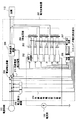
電力変換装置101は、相互に直列接続され直流電力を交流電力に変換する複数の単位変換器102と、単位変換器102の出力端に接続されたコンデンサ103と、コンデンサ103と電源系統111とを接続する変圧器104と、系統電圧を検出する電圧検出装置106と、コンデンサ103の電圧を検出する電圧検出装置107と、系統電流を検出する系統電流検出装置108と、系統に瞬低が発生したことを検出した場合に系統電流のフィードフォワード制御を行うとともに瞬低直前のコンデンサ電圧ベクトル振幅および系統相電圧ベクトル位相をそれぞれコンデンサ電圧振幅指令値およびコンデンサ電圧位相指令値とするコンデンサ電圧フィードバック制御により過渡時も安定にコンデンサ電圧を制御する制御装置105とを備えている。   The power conversion device 101 includes a plurality of unit converters 102 connected in series with each other to convert DC power into AC power, a capacitor 103 connected to an output terminal of the unit converter 102, a capacitor 103, and a power supply system 111. Transformer 104 to be connected, voltage detection device 106 for detecting the system voltage, voltage detection device 107 for detecting the voltage of the capacitor 103, system current detection device 108 for detecting the system current, and an instantaneous drop occurred in the system When this is detected, feed-forward control of the system current is performed, and transients are made by capacitor voltage feedback control in which the capacitor voltage vector amplitude and system phase voltage vector phase immediately before the voltage sag are set to the capacitor voltage amplitude command value and the capacitor voltage phase command value, respectively. And a control device 105 that stably controls the capacitor voltage. There.

単位変換器102は、互いに直列接続されている。直列接続された両端の単位変換器102は、SMESコイルからなる電流源110の両端にそれぞれ接続されている。単位変換器102の出力端子間には、コンデンサ103が接続されている。コンデンサ103は、変圧器104の2次側端子に接続される。各変圧器104の1次側の一方の端子は電源系統111の各相の電源ラインに接続され、他の端子は他の変圧器104の一方の端子と互いに接続されている。   The unit converters 102 are connected in series with each other. The unit converters 102 at both ends connected in series are respectively connected to both ends of a current source 110 formed of a SMES coil. A capacitor 103 is connected between the output terminals of the unit converter 102. Capacitor 103 is connected to the secondary side terminal of transformer 104. One terminal on the primary side of each transformer 104 is connected to the power line of each phase of the power supply system 111, and the other terminal is connected to one terminal of the other transformer 104.

(作用)
制御装置105は、電圧検出装置106を介して電源系統111の線間電圧を検出すると共に、電圧検出装置107を介して各単位変換器102の出力端のコンデンサ103の電圧を検出する。
(Function)
The control device 105 detects the line voltage of the power supply system 111 via the voltage detection device 106 and detects the voltage of the capacitor 103 at the output terminal of each unit converter 102 via the voltage detection device 107.

制御装置105は、検出した系統電圧信号から算出した系統電圧ベクトルの大きさが、基準値より小さい場合は、系統に瞬低が発生したと判断し、系統連系装置109を開放し、負荷112を電源系統111から遮断する。   When the magnitude of the system voltage vector calculated from the detected system voltage signal is smaller than the reference value, the control apparatus 105 determines that an instantaneous drop has occurred in the system, opens the system interconnection apparatus 109, and loads the load 112. Is disconnected from the power supply system 111.

制御装置105は、電圧検出装置106により検出した3相系統線間電圧信号を入力し、3相2相変換により静止座標系における水平軸方向の基準座標軸に対して90度位相が遅れた系統線間電圧ベクトルを生成する。この90度位相が遅れた系統線間電圧ベクトルの位相に60度を加算することにより、電源系統111の相電圧ベクトルの位相を算出する。瞬低を検出した場合、瞬低直前の相電圧ベクトルの位相をコンデンサ電圧ベクトル位相指令信号とする。また、瞬低発生直前のコンデンサ103の電圧ベクトルの大きさをコンデンサ電圧振幅指令信号とする。このようにして算出したコンデンサ電圧振幅指令信号とコンデンサ電圧ベクトル位相指令信号に基づいて、コンデンサ103の電圧をフィードバック制御する。   The control device 105 inputs the voltage signal between the three-phase system lines detected by the voltage detection device 106, and the system line whose phase is delayed by 90 degrees with respect to the reference coordinate axis in the horizontal axis direction in the stationary coordinate system by the three-phase two-phase conversion. Generate an inter-voltage vector. The phase of the phase voltage vector of the power supply system 111 is calculated by adding 60 degrees to the phase of the system line voltage vector delayed by 90 degrees. When a voltage drop is detected, the phase of the phase voltage vector immediately before the voltage drop is used as the capacitor voltage vector phase command signal. Further, the magnitude of the voltage vector of the capacitor 103 immediately before the occurrence of the instantaneous drop is used as the capacitor voltage amplitude command signal. Based on the capacitor voltage amplitude command signal and capacitor voltage vector phase command signal thus calculated, the voltage of the capacitor 103 is feedback-controlled.

また制御装置105は、系統電流の検出値を用いたフィードフォワード制御により過渡応答性能を改善する。
この結果、電力変換装置101は、電源系統111に瞬低が発生した場合、所定の時間の間、負荷112に対して安定に電力供給を継続し、瞬低補償制御を行う。
Further, the control device 105 improves the transient response performance by feedforward control using the detected value of the system current.
As a result, when a voltage sag occurs in the power supply system 111, the power conversion device 101 continuously supplies power to the load 112 for a predetermined time and performs sag compensation control.

(効果)
本実施の形態の電力変換装置によれば、大容量化のため複数の単位変換器102を互いに直列接続することにより、SMESコイルの直流電圧を大きく直流電流を小さくすることが可能となる。これにより従来の並列方式のSMES用電力変換器で必要であった横流抑制リアクトルと制御が不要となり、電力変換装置の寸法、重量、コストを低減することができる。また直流電流容量が低減するためSMESコイルと冷却装置の電流容量とコストを低減することができる。
(effect)
According to the power conversion device of the present embodiment, it is possible to increase the DC voltage of the SMES coil and decrease the DC current by connecting a plurality of unit converters 102 in series to increase the capacity. This eliminates the need for the cross current suppression reactor and control required in the conventional parallel-type SMES power converter, thereby reducing the size, weight, and cost of the power converter. Further, since the direct current capacity is reduced, the current capacity and cost of the SMES coil and the cooling device can be reduced.

更に、系統電流の検出値を用いたフィードフォワード制御により、過渡応答性能を改善することが可能となり、系統連系装置109のOFF時に系統に過電流が流れたり、負荷電圧が低下したりする問題を解決し、低コストで高性能な瞬低補償用SMES電力変換装置を提供することができる。   Furthermore, the feedforward control using the detected value of the system current makes it possible to improve the transient response performance, and when the system interconnection device 109 is OFF, the overcurrent flows through the system or the load voltage decreases. Thus, it is possible to provide a SMES power conversion device for low voltage, high performance instantaneous voltage compensation.

(第2の実施の形態)
本発明の第2の実施の形態を図2と図3を参照して説明する。
(構成)
図2は本実施の形態の電力変換装置201の構成を示す。
(Second Embodiment)
A second embodiment of the present invention will be described with reference to FIGS.
(Constitution)
FIG. 2 shows a configuration of the power conversion device 201 of the present embodiment.

負荷112は系統連系装置209を介して電源系統111に接続され、系統連系装置209と負荷112の間に電力変換装置201が接続されている。   The load 112 is connected to the power supply system 111 via the grid interconnection device 209, and the power conversion device 201 is connected between the grid interconnection device 209 and the load 112.

電力変換装置201は、単位変換器202と、コンデンサ203と、三巻変圧器204と、制御装置205と、電源系統111の系統線間電圧を検出する電圧検出装置206と、各単位変換器202の交流出力端子間に接続された電圧検出装置207と、電源系統111の3相交流電流を検出する電流検出装置208と、負荷112と電力変換装置201とを電源系統111に接続する系統連系装置209とを備えている。   The power conversion device 201 includes a unit converter 202, a capacitor 203, a three-winding transformer 204, a control device 205, a voltage detection device 206 that detects a system line voltage of the power supply system 111, and each unit converter 202. A voltage detection device 207 connected between the AC output terminals, a current detection device 208 that detects a three-phase AC current of the power supply system 111, and a grid interconnection that connects the load 112 and the power conversion device 201 to the power supply system 111. Device 209.

この実施の形態では、6台の単位変換器202を互いに直列接続して電力変換装置201を構成している。直列接続された両端の単位変換器202は、SMESコイルからなる電流源110の両端にそれぞれ接続される。単位変換器202の出力端子間には、コンデンサ203が接続されている。コンデンサ203は、三巻変圧器204の2次側の巻線に接続されている。三巻変圧器204の1次側の一方の端子は、電源系統111の各相の電源ラインに接続され、他の端子は他の三巻変圧器204の他方の端子と互いに接続されている。   In this embodiment, six unit converters 202 are connected in series to constitute a power conversion device 201. The unit converters 202 at both ends connected in series are respectively connected to both ends of the current source 110 formed of a SMES coil. A capacitor 203 is connected between the output terminals of the unit converter 202. The capacitor 203 is connected to the secondary winding of the three-winding transformer 204. One terminal on the primary side of the three-turn transformer 204 is connected to the power line of each phase of the power supply system 111, and the other terminal is connected to the other terminal of the other three-turn transformer 204.

図3に本実施の形態における単位変換器202の構成を示す。
単位変換器202は、単相ブリッジの構成である。各アームは、逆阻止用のダイオード301とスイッチング素子302からなる。この単位変換器202は、一般的な単相ブリッジと汎用の素子を使用することにより低コストな電力変換器となっている。
FIG. 3 shows the configuration of unit converter 202 in the present embodiment.
The unit converter 202 has a single-phase bridge configuration. Each arm includes a reverse blocking diode 301 and a switching element 302. The unit converter 202 is a low-cost power converter by using a general single-phase bridge and a general-purpose element.

(作用)
(系統電圧、コンデンサ電圧、系統電流の検出)
制御装置205は、電圧検出装置206を介して系統電圧を検出すると共に、電圧検出装置207を介して各単位変換器202の出力端のコンデンサ203の電圧を検出する。また制御装置205は、電流検出装置208を介して、3相の系統電流を検出する。
(Function)
(Detection of system voltage, capacitor voltage, system current)
The control device 205 detects the system voltage via the voltage detection device 206 and also detects the voltage of the capacitor 203 at the output terminal of each unit converter 202 via the voltage detection device 207. Further, the control device 205 detects a three-phase system current via the current detection device 208.

(コンデンサ電圧位相指令信号の生成)
制御装置205は、電圧検出装置206を介して検出した3相系統電圧を1次遅れフィルタに入力する。
制御装置205は、1次遅れフィルタによって得られた1次遅れ出力信号を3相2相変換し、位相が90度遅れた2相系統線間電圧信号を生成する。制御装置205はこの2相系統線間電圧信号から系統線間電圧ベクトルの位相を算出する。制御装置205は、この系統線間電圧ベクトル位相信号にπ/3[rad]を加算することにより、系統相電圧ベクトルの位相信号を生成する。そして制御装置205は、この系統相電圧ベクトルの位相信号をコンデンサ電圧ベクトル位相指令信号として使用する。
(Generation of capacitor voltage phase command signal)
The control device 205 inputs the three-phase system voltage detected via the voltage detection device 206 to the primary delay filter.
The control device 205 performs three-phase to two-phase conversion on the first-order lag output signal obtained by the first-order lag filter, and generates a two-phase system line voltage signal whose phase is delayed by 90 degrees. The control device 205 calculates the phase of the system line voltage vector from the two-phase system line voltage signal. The control device 205 generates a phase signal of the system phase voltage vector by adding π / 3 [rad] to this system line voltage vector phase signal. The control device 205 uses the phase signal of the system phase voltage vector as the capacitor voltage vector phase command signal.

(コンデンサ電圧のフィードバック)
制御装置205は、検出した1段目と2段目のコンデンサ203の電圧を加算して3相の1相であるU相のコンデンサ電圧を生成する。
(Capacitor voltage feedback)
The control device 205 adds the detected voltages of the first-stage and second-stage capacitors 203 to generate a U-phase capacitor voltage that is one of the three phases.

また制御装置は、3段目と4段目のコンデンサ203の電圧を加算して3相の1相であるV相のコンデンサ電圧を生成する。   Further, the control device adds the voltages of the capacitors 203 in the third and fourth stages to generate a V-phase capacitor voltage that is one of the three phases.

更に制御装置205は、5段目と6段目のコンデンサ203の電圧を加算して3相の1相であるW相のコンデンサ電圧を生成する。制御装置205は、UVW3相のコンデンサ電圧信号を3相2相変換して2相コンデンサ電圧を生成する。   Further, the control device 205 adds the voltages of the capacitors 203 in the fifth and sixth stages to generate a W-phase capacitor voltage that is one of the three phases. The control device 205 performs three-phase to two-phase conversion on the UVW three-phase capacitor voltage signal to generate a two-phase capacitor voltage.

制御装置205は、2相コンデンサ電圧の2乗和の正の平方根をコンデンサ電圧ベクトルの大きさとして算出する。   The control device 205 calculates the positive square root of the square sum of the two-phase capacitor voltage as the magnitude of the capacitor voltage vector.

制御装置205は、算出したコンデンサ電圧ベクトルの大きさを1次遅れフィルタを通すことにより、3相コンデンサ電圧振幅指令信号として出力する。そして3相コンデンサ電圧振幅指令信号を3相2相変換し、2相コンデンサ電圧振幅信号を出力する。   The control device 205 outputs the magnitude of the calculated capacitor voltage vector as a three-phase capacitor voltage amplitude command signal by passing through the first-order lag filter. The three-phase capacitor voltage amplitude command signal is three-phase to two-phase converted, and a two-phase capacitor voltage amplitude signal is output.

制御装置205は、2相コンデンサ電圧振幅信号を前記コンデンサ電圧ベクトル位相指令信号によりDQ変換して、DQコンデンサ電圧振幅信号を出力する。DQ変換は、静止座標系の成分を系統電圧と同一周波数で回転する回転座標系へ変換する座標変換である。   The control device 205 DQ-converts the two-phase capacitor voltage amplitude signal with the capacitor voltage vector phase command signal, and outputs a DQ capacitor voltage amplitude signal. The DQ conversion is a coordinate conversion for converting a stationary coordinate system component into a rotating coordinate system that rotates at the same frequency as the system voltage.

(系統電流フィードフォワード制御)
制御装置205は、検出した3相系統電流を1次遅れフィルタに入力し、1次遅れフィルタ出力の3相系統電流信号を用いて、3相2相変換する。
制御装置205は、3相2相変換した2相系統電流をコンデンサ電圧ベクトル位相指令信号を用いてDQ変換を行ない、DQ系統電流信号を出力する。
(System current feedforward control)
The control device 205 inputs the detected three-phase system current to the first-order lag filter, and performs three-phase to two-phase conversion using the three-phase system current signal output from the first-order lag filter.
The control device 205 performs DQ conversion on the two-phase system current obtained by three-phase to two-phase conversion using the capacitor voltage vector phase command signal, and outputs a DQ system current signal.

(瞬低検出判断)
制御装置205は、2相系統線間電圧信号の各成分の2乗和の正の平方根を計算し、系統線間電圧ベクトル振幅信号として出力する。そして、この系統線間電圧ベクトル振幅信号がしいき値以下であれば、系統に瞬低が発生したと判断し、瞬低検出信号を出力する。
(Instantaneous voltage drop detection judgment)
The control device 205 calculates the positive square root of the square sum of each component of the two-phase system line voltage signal and outputs it as a system line voltage vector amplitude signal. If this system line voltage vector amplitude signal is below the threshold value, it is determined that a voltage sag has occurred in the system, and a voltage sag detection signal is output.

(待機制御)
制御装置205は、電源系統111が健全な場合は各単位変換器202の上下アームを導通することにより、電流源110(SMESコイル)の電流を保持し、待機する。
(Standby control)
When the power supply system 111 is healthy, the control device 205 conducts the upper and lower arms of each unit converter 202 to hold the current of the current source 110 (SMES coil) and stands by.

(瞬低補償制御)
もし電源系統111に瞬低が発生した場合は、制御装置205は、瞬低直前の3相コンデンサ電圧振幅指令信号とコンデンサ電圧ベクトル位相指令信号を保持し、系統電源周波数によりコンデンサ電圧ベクトル位相指令信号の位相を進める。
(Instantaneous voltage drop compensation control)
If a voltage drop occurs in the power supply system 111, the control device 205 holds the three-phase capacitor voltage amplitude command signal and the capacitor voltage vector phase command signal immediately before the voltage drop, and the capacitor voltage vector phase command signal by the system power supply frequency. Advance the phase of.

制御装置205は、3相コンデンサ電圧振幅指令信号とコンデンサ電圧ベクトル位相指令信号を用いて3相コンデンサ電圧指令信号を算出する。
制御装置205は、3相コンデンサ電圧指令信号を3相2相変換し、コンデンサ電圧ベクトル位相指令信号によりDQ変換し、DQコンデンサ電圧指令信号を生成する。
Control device 205 calculates a three-phase capacitor voltage command signal using the three-phase capacitor voltage amplitude command signal and the capacitor voltage vector phase command signal.
The control device 205 performs three-phase to two-phase conversion on the three-phase capacitor voltage command signal, performs DQ conversion on the capacitor voltage vector phase command signal, and generates a DQ capacitor voltage command signal.

また制御装置205は、2相コンデンサ電圧検出信号に対してコンデンサ電圧ベクトル位相指令信号を用いてDQコンデンサ電圧検出信号に変換する。
制御装置205は、DQコンデンサ電圧指令信号とDQコンデンサ電圧検出信号を用いてPI制御により、コンデンサ電圧制御出力信号を生成する。
The control device 205 converts the two-phase capacitor voltage detection signal into a DQ capacitor voltage detection signal using the capacitor voltage vector phase command signal.
The control device 205 generates a capacitor voltage control output signal by PI control using the DQ capacitor voltage command signal and the DQ capacitor voltage detection signal.

制御装置205は、コンデンサ電圧制御出力信号とDQ系統電流信号を加算して、DQ電流指令信号を生成する。
制御装置205は、系統電流のフィードフォワード制御であるDQ系統電流信号を加算することにより、高速に系統連系装置209をOFFし、電源系統111を遮断する。
The control device 205 adds the capacitor voltage control output signal and the DQ system current signal to generate a DQ current command signal.
The control device 205 adds the DQ system current signal that is the feedforward control of the system current, thereby turning off the system interconnection device 209 at high speed and shutting off the power system 111.

これにより、電力変換装置201は、瞬低期間中、負荷112に対し安定に電力供給を継続する。この結果、電力変換装置201は、電源系統111に瞬低が発生した場合、所定の時間の間、負荷112に対して安定に電力供給を継続し、瞬低補償制御を行う。   As a result, the power conversion device 201 continues to supply power stably to the load 112 during the sag period. As a result, when a power sag occurs in the power supply system 111, the power conversion device 201 stably supplies power to the load 112 for a predetermined time, and performs power sag compensation control.

(効果)
この第2の実施の形態によれば、複数の単相ブリッジ回路を使用することにより、容易にSMES用電力変換装置を構成できる。この結果、低コストな電力変換装置を構築できると共に、システムの信頼性を改善することができる。また直流電流容量が低減するためSMESコイルと冷却装置の電流容量とコストを低減することができる。
(effect)
According to the second embodiment, a SMES power converter can be easily configured by using a plurality of single-phase bridge circuits. As a result, a low-cost power conversion device can be constructed and the reliability of the system can be improved. Further, since the direct current capacity is reduced, the current capacity and cost of the SMES coil and the cooling device can be reduced.

更に、系統電流の検出値を用いたフィードフォワード制御により、過渡応答性能を改善することが可能となり、系統連系装置209のOFF時に系統に過電流が流れたり、負荷電圧が低下したりする問題を解決し、低コストで高性能な瞬低補償用SMES電力変換装置を提供することができる。   Furthermore, the feedforward control using the detected value of the system current makes it possible to improve the transient response performance, and when the system interconnection device 209 is OFF, the overcurrent flows through the system or the load voltage decreases. Thus, it is possible to provide a SMES power conversion device for low voltage, high performance instantaneous voltage compensation.

(第3の実施の形態)
本発明の第3の実施の形態を図4から図7を参照して説明する。本実施の形態は、図2に示した制御装置205に関する。
(Third embodiment)
A third embodiment of the present invention will be described with reference to FIGS. The present embodiment relates to the control device 205 shown in FIG.

(構成)
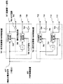
本実施の形態における制御装置205は、図4に示すように、コンデンサ電圧制御装置401と、電流指令制御装置402と、PWM制御装置403とから構成されている。
(Constitution)
As shown in FIG. 4, the control device 205 in the present embodiment includes a capacitor voltage control device 401, a current command control device 402, and a PWM control device 403.

コンデンサ電圧制御装置401は、図5に示すように、電圧ベクトル位相を90度遅らせる3相2相変換手段501a,501b,501c,501dと、コンデンサ電圧振幅検出手段502と、コンデンサ電圧振幅制御手段503と、系統線間電圧位相検出手段504と、加算器525と、コンデンサ電圧位相制御手段505と、コンデンサ電圧指令生成手段506と、2相DQ変換手段507a,507b,507cと、減算手段508と、PI制御手段509と、1次遅れフィルタ523a,523b,523cと、加算器525と、瞬低判定手段526とを備えている。   As shown in FIG. 5, the capacitor voltage control device 401 includes three-phase / two-phase conversion means 501a, 501b, 501c, 501d for delaying the voltage vector phase by 90 degrees, capacitor voltage amplitude detection means 502, and capacitor voltage amplitude control means 503. System line voltage phase detection means 504, adder 525, capacitor voltage phase control means 505, capacitor voltage command generation means 506, two-phase DQ conversion means 507a, 507b, 507c, subtraction means 508, PI control means 509, primary delay filters 523 a, 523 b, 523 c, an adder 525, and instantaneous drop determination means 526 are provided.

電流指令制御装置402は、図6に示すように、リミッタ手段601と、ベクトル・リミット手段602と、最小ONパルス幅制御手段603と、DQ2相変換手段604と、2相3相変換手段605と、3相電流指令制御手段606とを備えている。   As shown in FIG. 6, the current command control device 402 includes a limiter unit 601, a vector limit unit 602, a minimum ON pulse width control unit 603, a DQ two-phase conversion unit 604, and a two-phase three-phase conversion unit 605. And three-phase current command control means 606.

図7に1相当りのPWM制御装置403の構成を示す。
PWM制御装置403は、1段目変換器PWM制御装置701と、2段目変換器PWM制御装置702とから構成されている。1段目変換器PWM制御装置701は、PWM制御装置703と、NOT回路704と、極性反転回路705とを備えている。2段目変換器PWM制御装置702は、1段目変換器PWM制御装置701と同じ構成であるが、キャリヤ信号711の位相が1段目変換器PWM制御装置701のキャリヤ信号706に対して90度遅れている。
FIG. 7 shows the configuration of one PWM control device 403.
The PWM controller 403 includes a first-stage converter PWM controller 701 and a second-stage converter PWM controller 702. The first-stage converter PWM control device 701 includes a PWM control device 703, a NOT circuit 704, and a polarity inversion circuit 705. The second stage converter PWM control device 702 has the same configuration as the first stage converter PWM control device 701, but the phase of the carrier signal 711 is 90 relative to the carrier signal 706 of the first stage converter PWM control device 701. It is late.

(作用)
図4に示すように、制御装置205を構成するコンデンサ電圧制御装置401は、3相コンデンサ電圧検出値404と系統線間電圧検出信号210を入力し、コンデンサ電圧制御の結果としてコンデンサ電圧制御DQ電流指令値405を出力する。ここで、3相コンデンサ電圧検出値404は、各相を構成する2段の単位変換器202の出力端コンデンサ203の電圧を加算し算出される3相電圧である。
(Function)
As shown in FIG. 4, the capacitor voltage control device 401 constituting the control device 205 inputs a three-phase capacitor voltage detection value 404 and a system line voltage detection signal 210, and the capacitor voltage control DQ current is obtained as a result of the capacitor voltage control. The command value 405 is output. Here, the three-phase capacitor voltage detection value 404 is a three-phase voltage calculated by adding the voltages of the output end capacitors 203 of the two-stage unit converter 202 constituting each phase.

電流指令制御装置402は、コンデンサ電圧制御DQ電流指令値405と系統電流フィードフォワード制御DQ電流指令値406を入力し、3相出力電流指令407を出力する。
PWM制御装置403は、3相出力電流指令407を入力し、U相1段目単位変換器ゲート信号408、U相2段目単位変換器ゲート信号409、V相1段目単位変換器ゲート信号410、V相2段目単位変換器ゲート信号411、W相1段目単位変換器ゲート信号412、W相2段目単位変換器ゲート信号413を各単位変換器202に対して出力する。
The current command control device 402 receives the capacitor voltage control DQ current command value 405 and the system current feedforward control DQ current command value 406 and outputs a three-phase output current command 407.
The PWM controller 403 receives a three-phase output current command 407, receives a U-phase first-stage unit converter gate signal 408, a U-phase second-stage unit converter gate signal 409, and a V-phase first-stage unit converter gate signal. 410, V phase second stage unit converter gate signal 411, W phase first stage unit converter gate signal 412, and W phase second stage unit converter gate signal 413 are output to each unit converter 202.

図5に示すように、コンデンサ電圧制御装置401を構成する3相2相変換手段501aは、3相コンデンサ電圧検出値404を入力し、静止2相座標系の2軸成分である2相コンデンサ電圧信号511に変換する。   As shown in FIG. 5, the three-phase to two-phase conversion means 501a constituting the capacitor voltage control device 401 receives the three-phase capacitor voltage detection value 404, and the two-phase capacitor voltage that is the two-axis component of the stationary two-phase coordinate system. Convert to signal 511.

コンデンサ電圧振幅検出手段502は、2相コンデンサ電圧信号511を入力し、2乗和の正の平方根をコンデンサ電圧振幅512として出力する。   Capacitor voltage amplitude detector 502 receives a two-phase capacitor voltage signal 511 and outputs the positive square root of the sum of squares as capacitor voltage amplitude 512.

1次遅れフィルタ523aは、コンデンサ電圧振幅512を入力し、コンデンサ電圧振幅512の高周波リプル成分を除去し、コンデンサ電圧振幅指令フィルタ出力値524を出力する。   The first-order lag filter 523a receives the capacitor voltage amplitude 512, removes the high frequency ripple component of the capacitor voltage amplitude 512, and outputs a capacitor voltage amplitude command filter output value 524.

コンデンサ電圧振幅制御手段503は、コンデンサ電圧振幅指令フィルタ出力値524と、瞬低発生信号522を入力し、瞬低が発生した場合は瞬低発生直前のコンデンサ電圧振幅指令フィルタ出力値524をコンデンサ電圧振幅指令値513として保持する。   Capacitor voltage amplitude control means 503 receives capacitor voltage amplitude command filter output value 524 and voltage sag occurrence signal 522. When voltage sag occurs, capacitor voltage amplitude command filter output value 524 immediately before the time of voltage sag is converted to capacitor voltage. This is held as the amplitude command value 513.

3相2相変換手段501bは、1次遅れフィルタ523bを介して3相の系統線間電圧検出信号210を入力し、系統線間電圧を90度位相遅れの電圧ベクトル信号に変換する。   The three-phase / two-phase conversion means 501b inputs the three-phase system line voltage detection signal 210 via the first-order lag filter 523b, and converts the system line voltage into a voltage vector signal having a phase delay of 90 degrees.

系統線間電圧位相検出手段504は、90度位相が遅れた電圧ベクトルを入力し、系統電圧位相信号を算出し出力する。加算器525は、系統電圧位相信号の位相とπ/3[rad]を加算し、系統相電圧位相信号514を出力する。   The line voltage phase detection means 504 receives a voltage vector whose phase is delayed by 90 degrees, calculates a system voltage phase signal, and outputs it. Adder 525 adds the phase of the system voltage phase signal and π / 3 [rad], and outputs system phase voltage phase signal 514.

コンデンサ電圧位相制御手段505は、系統相電圧位相信号514と瞬低発生信号522とを入力し、瞬低が発生した場合は、瞬低発生直前の系統相電圧位相信号514をコンデンサ電圧位相指令信号の基準値として保持し、系統電圧の定格周波数で位相を進め、コンデンサ電圧位相指令信号515を出力する。
コンデンサ電圧指令生成手段506は、コンデンサ電圧振幅指令値513とコンデンサ電圧位相指令信号515とを入力し、3相コンデンサ電圧指令値516を出力する。
Capacitor voltage phase control means 505 inputs system phase voltage phase signal 514 and voltage sag occurrence signal 522, and when voltage sag occurs, system voltage phase signal 514 immediately before the occurrence of voltage sag is used as capacitor voltage phase command signal. And the phase is advanced at the rated frequency of the system voltage, and a capacitor voltage phase command signal 515 is output.
Capacitor voltage command generation means 506 receives capacitor voltage amplitude command value 513 and capacitor voltage phase command signal 515 and outputs a three-phase capacitor voltage command value 516.

3相2相変換手段501cは、3相コンデンサ電圧指令値516を入力し、静止2相成分のDQコンデンサ電圧指令値517を出力する。
2相DQ変換手段507aは2相コンデンサ電圧指令値517とコンデンサ電圧位相指令信号515とを入力しDQコンデンサ電圧指令値518を出力する。
The three-phase / two-phase conversion means 501c receives a three-phase capacitor voltage command value 516 and outputs a DQ capacitor voltage command value 517 of a stationary two-phase component.
The two-phase DQ conversion means 507a receives the two-phase capacitor voltage command value 517 and the capacitor voltage phase command signal 515 and outputs the DQ capacitor voltage command value 518.

減算手段508は、DQコンデンサ電圧指令値518からDQコンデンサ電圧検出値519を減算することにより、DQコンデンサ電圧偏差520を算出する。
PI制御手段509はDQコンデンサ電圧偏差520を入力し、PI(積算および積分)制御の結果として、コンデンサ電圧制御DQ電流指令値405を出力する。
Subtraction means 508 calculates DQ capacitor voltage deviation 520 by subtracting DQ capacitor voltage detection value 519 from DQ capacitor voltage command value 518.
The PI control means 509 receives the DQ capacitor voltage deviation 520 and outputs a capacitor voltage control DQ current command value 405 as a result of PI (integration and integration) control.

3相2相変換501dは、3相の系統電流検出信号211を入力し、3相2相変換により2相の系統電流検出信号を出力する。
2相DQ変換手段507cは、2相の系統電流検出信号を入力し、DQ変換により系統電流フィードフォワード制御DQ電流指令値406を出力する。
The three-phase / two-phase conversion 501d receives a three-phase system current detection signal 211 and outputs a two-phase system current detection signal by the three-phase / two-phase conversion.
The two-phase DQ conversion means 507c receives a two-phase grid current detection signal and outputs a grid current feedforward control DQ current command value 406 by DQ conversion.

図6に示すように、電流指令制御装置402を構成するリミッタ手段601は、系統電流フィードフォワード制御DQ電流指令値406とコンデンサ電圧制御DQ電流指令値405を加算して生成するDQ電流指令値600を入力し、D軸電流指令値とQ軸電流指令値との絶対値が、それぞれのリミット値を超えた場合は、DQ軸電流指令値を所定のリミット値に制限したリミットDQ電流指令607を出力する。   As shown in FIG. 6, the limiter means 601 constituting the current command control device 402 adds a system current feedforward control DQ current command value 406 and a capacitor voltage control DQ current command value 405 to generate a DQ current command value 600. When the absolute value of the D-axis current command value and the Q-axis current command value exceeds the respective limit values, a limit DQ current command 607 that limits the DQ-axis current command value to a predetermined limit value is displayed. Output.

ベクトル・リミット手段602は、リミットDQ電流指令607を入力し、D軸とQ軸のリミット電流指令から構成される電流ベクトルの振幅が規定値を超えた場合は、電流ベクトルの振幅が規定値になるように、D軸とQ軸のリミット電流指令を変換し、ベクトル・リミットDQ電流指令608を出力する。   The vector limit means 602 receives the limit DQ current command 607, and when the amplitude of the current vector composed of the D-axis and Q-axis limit current commands exceeds the specified value, the amplitude of the current vector becomes the specified value. Thus, the limit current command for the D axis and the Q axis is converted, and the vector limit DQ current command 608 is output.

最小ONパルス幅制御手段603は、ベクトル・リミットDQ電流指令608を入力し、この電流指令を用いたPWM制御の結果、電力変換器202を構成する素子により規定される最小ONパルス幅より短いPWMパルスが発生しないように、ベクトル・リミットDQ電流指令値を制限した値である最小ONパルス幅制御DQ電流指令609を出力する。   The minimum ON pulse width control means 603 receives the vector limit DQ current command 608, and as a result of PWM control using this current command, the PWM shorter than the minimum ON pulse width defined by the elements constituting the power converter 202. A minimum ON pulse width control DQ current command 609, which is a value obtained by limiting the vector limit DQ current command value, is output so that no pulse is generated.

DQ2相変換手段604は、最小ONパルス幅制御DQ電流指令609と、コンデンサ電圧位相指令値515とを入力し、2相電流指令610を出力する。
2相3相変換手段605は、2相電流指令610を入力し、2相3相変換を行ない瞬低補償制御用3相出力電流指令612を出力する。
The DQ two-phase conversion means 604 receives the minimum ON pulse width control DQ current command 609 and the capacitor voltage phase command value 515 and outputs a two-phase current command 610.
The two-phase / three-phase conversion means 605 receives the two-phase current command 610, performs two-phase / three-phase conversion, and outputs a voltage drop compensation control three-phase output current command 612.

3相電流指令制御手段606は、待機制御用3相出力電流指令613と瞬低補償制御用3相出力電流指令612と瞬低発生信号522を入力する。3相電流指令制御手段606は、瞬低発生信号522が瞬低発生の値にセットされていなければ、待機制御用3相出力電流指令613を3相出力電流指令407として出力する。瞬低発生信号522が瞬低発生の値にセットされていれば、瞬低補償制御用3相出力電流指令612を3相出力電流指令407として出力する。   The three-phase current command control means 606 receives the standby control three-phase output current command 613, the sag compensation control three-phase output current command 612, and the sag occurrence signal 522. The three-phase current command control means 606 outputs the standby control three-phase output current command 613 as the three-phase output current command 407 unless the voltage sag occurrence signal 522 is set to the value of the voltage sag occurrence. If the voltage sag occurrence signal 522 is set to the value of the voltage sag occurrence, the voltage sag compensation control three-phase output current command 612 is output as the three-phase output current command 407.

図7に示すように、1段目変換器PWM制御装置701を構成するPWM信号発生器703は、3相出力電流指令407の一相当りの電流指令信号と、キャリヤ信号706を入力し、3相出力電流指令407の一相当りの電流指令信号がキャリヤ信号706より大きければスイッチング素子をONするPWM信号を出力し、そうでなければ、スイッチング素子をOFFするPWM信号を出力する。発生したPWM信号は、NOT回路704を介して、単相ブリッジ回路の上アームを構成するスイッチング素子のゲート信号707と708として出力される。   As shown in FIG. 7, the PWM signal generator 703 constituting the first-stage converter PWM control device 701 receives a current command signal corresponding to one of the three-phase output current commands 407 and the carrier signal 706. If the current command signal corresponding to one of the phase output current commands 407 is larger than the carrier signal 706, a PWM signal for turning on the switching element is output, and if not, a PWM signal for turning off the switching element is output. The generated PWM signal is output via the NOT circuit 704 as gate signals 707 and 708 of the switching elements constituting the upper arm of the single-phase bridge circuit.

単相ブリッジ回路の下側アームを構成するスイッチング素子に対するPWM制御は、1相分の電流指令信号407を極性反転回路705により反転させた電流指令信号を用いて行なわれる。反転された電流指令信号とキャリヤ信号706によりPWM制御され、単相ブリッジ回路の下アームを構成するスイッチング素子に対するゲート信号が出力される。   PWM control for the switching elements constituting the lower arm of the single-phase bridge circuit is performed using a current command signal obtained by inverting the current command signal 407 for one phase by the polarity inverting circuit 705. PWM control is performed by the inverted current command signal and carrier signal 706, and a gate signal for the switching element constituting the lower arm of the single-phase bridge circuit is output.

2段目の単位変換器に対するPWM制御は、キャリヤ信号711の位相を1段目の単位変換器に対するPWM制御におけるキャリヤ信号706の位相から90°ずらすことにより実現する。1段目と2段目の単位変換器に対するPWM制御キャリヤ信号に90°の位相差を設けるのは、発生する高調波を抑制するためである。   The PWM control for the second stage unit converter is realized by shifting the phase of the carrier signal 711 by 90 ° from the phase of the carrier signal 706 in the PWM control for the first stage unit converter. The reason why the phase difference of 90 ° is provided in the PWM control carrier signal for the first-stage and second-stage unit converters is to suppress the generated harmonics.

他相のPWM制御は、他の相の電流指令信号407を用いて、同様に実現する。
上記の制御の結果、各単位変換器の出力端フィルタコンデンサ電圧を系統が瞬低する直前の電圧に制御することができる。
本制御により系統瞬低時に負荷に対して所要の電力補償を実現することが可能となる。
The other-phase PWM control is similarly realized by using the current command signal 407 of the other phase.
As a result of the above control, the output-end filter capacitor voltage of each unit converter can be controlled to a voltage immediately before the system instantaneously drops.
This control makes it possible to realize the required power compensation for the load when the system is instantaneously low.

(効果)
この第3の実施の形態の電力変換装置によれば、従来の三角波比較PWM制御を使用することができる。この結果、制御系のコストを抑制することができ、低コストな電力変換装置を提供することができる。また直流電流容量が低減するためSMESコイルと冷却装置の電流容量とコストを低減することができる。
(effect)
According to the power converter of the third embodiment, the conventional triangular wave comparison PWM control can be used. As a result, the cost of the control system can be suppressed, and a low-cost power conversion device can be provided. Further, since the direct current capacity is reduced, the current capacity and cost of the SMES coil and the cooling device can be reduced.

更に、系統電流の検出値を用いたフィードフォワード制御により、過渡応答性能を改善することが可能となり、系統連系装置209のOFF時に系統に過電流が流れたり、負荷電圧が低下する問題を解決し、低コストで高性能な瞬低補償用SMES電力変換装置を提供することができる。   Furthermore, the feedforward control using the detected value of the system current makes it possible to improve the transient response performance, and solves the problem that the overcurrent flows through the system or the load voltage decreases when the system interconnection device 209 is OFF. In addition, it is possible to provide a SMES power converter for compensating for a sag with high performance at low cost.

(第4の実施の形態)
本発明の第4の実施の形態を図8から図10を参照して説明する。本実施の形態も第3の実施の形態と同様に図2に示した制御装置205に関する。
(Fourth embodiment)
A fourth embodiment of the present invention will be described with reference to FIGS. The present embodiment also relates to the control device 205 shown in FIG. 2 as in the third embodiment.

(構成)
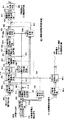
本実施の形態における制御装置205は、図8に示すように、模擬系統電流制御装置801と、電流指令制御装置802と、PWM制御装置403から構成されている。
(Constitution)
As shown in FIG. 8, the control device 205 in the present embodiment includes a simulated system current control device 801, a current command control device 802, and a PWM control device 403.

模擬系統電流制御装置801は、図9に示すように、系統線間電圧位相検出手段901と、入力した電圧ベクトルの位相を90度遅らせる3相2相変換手段902a,902b,902cと、コンデンサ電圧振幅検出手段903と、1次遅れフィルタ927と、コンデンサ電圧振幅制御手段904と、コンデンサ電圧位相制御手段906と、模擬系統3相電圧生成手段907と、2相DQ変換手段908a,908bと、減算手段909と、模擬系統電流算出手段910と、PI制御手段911とを備えている。   As shown in FIG. 9, the simulated system current control device 801 includes a system line voltage phase detection unit 901, a three-phase / two-phase conversion unit 902 a, 902 b, 902 c that delays the phase of the input voltage vector by 90 degrees, and a capacitor voltage. Amplitude detection means 903, first-order lag filter 927, capacitor voltage amplitude control means 904, capacitor voltage phase control means 906, simulated system three-phase voltage generation means 907, two-phase DQ conversion means 908a, 908b, subtraction Means 909, simulated system current calculation means 910, and PI control means 911 are provided.

模擬系統電流算出手段910は、図10に示すように、減算器1001a,1001bと、除算器1002と、乗算器1003a,1003bと、積分器1004と、遅れ要素1005とを備えている。   As shown in FIG. 10, the simulated system current calculation means 910 includes subtractors 1001a and 1001b, a divider 1002, multipliers 1003a and 1003b, an integrator 1004, and a delay element 1005.

(作用)
図8に示すように、制御装置205の模擬系統電流制御装置801は、3相コンデンサ電圧検出値404を入力し、模擬系統電流制御の結果としてPI制御出力DQ電流指令値805を出力する。ここで、3相コンデンサ電圧検出値404は、各単位変換器の出力コンデンサ電圧のうち、同種の相間のコンデンサ電圧を互いに加算した値である。
(Function)
As shown in FIG. 8, the simulated system current control device 801 of the control device 205 inputs a three-phase capacitor voltage detection value 404 and outputs a PI control output DQ current command value 805 as a result of the simulated system current control. Here, the three-phase capacitor voltage detection value 404 is a value obtained by adding the capacitor voltages between the same type of the output capacitor voltages of the unit converters.

電流指令制御装置802は、PI制御出力DQ電流指令値805と系統電流検出信号211を入力し、3相出力電流指令407を出力する。   The current command control device 802 receives the PI control output DQ current command value 805 and the system current detection signal 211 and outputs a three-phase output current command 407.

PWM制御装置403は、3相出力電流指令407を入力し、U相1段目単位変換器ゲート信号408、U相2段目単位変換器ゲート信号409、V相1段目単位変換器ゲート信号410、V相2段目単位変換器ゲート信号411、W相1段目単位変換器ゲート信号412、W相2段目単位変換器ゲート信号413を各単位変換器202に対して出力する。   The PWM controller 403 receives a three-phase output current command 407, receives a U-phase first-stage unit converter gate signal 408, a U-phase second-stage unit converter gate signal 409, and a V-phase first-stage unit converter gate signal. 410, V phase second stage unit converter gate signal 411, W phase first stage unit converter gate signal 412, and W phase second stage unit converter gate signal 413 are output to each unit converter 202.

図9に示すように、模擬系統電流制御装置801の3相2相変換手段902aは、3相コンデンサ電圧検出値404を入力し、静止2相座標系の2軸成分である二相コンデンサ電圧信号914に変換する。   As shown in FIG. 9, the three-phase two-phase conversion means 902a of the simulated system current control device 801 receives a three-phase capacitor voltage detection value 404, and a two-phase capacitor voltage signal that is a biaxial component of a stationary two-phase coordinate system. Convert to 914.

コンデンサ電圧振幅検出手段903は、二相コンデンサ電圧信号914を入力し、2乗和の正の平方根をコンデンサ電圧振幅915として出力する。1次遅れフィルタ927は、コンデンサ電圧振幅915を入力し、高周波リプルを除去したコンデンサ電圧振幅指令フィルタ出力値928を出力する。   The capacitor voltage amplitude detector 903 receives the two-phase capacitor voltage signal 914 and outputs the positive square root of the sum of squares as the capacitor voltage amplitude 915. The first-order lag filter 927 receives the capacitor voltage amplitude 915 and outputs a capacitor voltage amplitude command filter output value 928 from which the high frequency ripple has been removed.

コンデンサ電圧振幅制御手段904は、コンデンサ電圧振幅指令フィルタ出力値928と、瞬低発生信号522とを入力し、瞬低が発生した場合は瞬低発生直前のコンデンサ電圧振幅915をコンデンサ電圧振幅指令値917として保持する。   Capacitor voltage amplitude control means 904 receives capacitor voltage amplitude command filter output value 928 and sag occurrence signal 522, and when sag occurs, capacitor voltage amplitude 915 immediately before the occurrence of sag is obtained as capacitor voltage amplitude command value. 917 is held.

系統線間電圧検出信号210は、1次遅れフィルタ523bを介して3相2相変換手段902cに入力される。
3相2相変換手段902cは、系統線間電圧検出信号210の1次遅れフィルタ出力値を入力し、2相系統線間電圧位相信号912を出力する。
The system line voltage detection signal 210 is input to the three-phase / two-phase conversion means 902c via the first-order lag filter 523b.
The three-phase / two-phase conversion means 902c receives the first-order lag filter output value of the system line voltage detection signal 210 and outputs a 2-phase system line voltage phase signal 912.

系統線間電圧位相検出手段901は、2相系統線間電圧位相信号912を入力し、系統線間電圧位相信号913を出力する。
加算器905は系統線間電圧位相信号913にπ/3[rad]を加算してコンデンサ電圧位相信号918を出力する。
The system line voltage phase detection means 901 receives the 2-phase system line voltage phase signal 912 and outputs the system line voltage phase signal 913.
The adder 905 adds π / 3 [rad] to the system voltage level signal 913 and outputs a capacitor voltage phase signal 918.

コンデンサ電圧位相制御手段906は、コンデンサ電圧位相信号918と瞬低発生信号522とを入力し、瞬低が発生した場合は、瞬低発生直前のコンデンサ電圧位相信号918をコンデンサ電圧位相指令信号の基準値として保持し、系統電圧の定格周波数で位相を進め、コンデンサ電圧位相指令信号919を出力する。   Capacitor voltage phase control means 906 receives capacitor voltage phase signal 918 and voltage sag occurrence signal 522, and when voltage sag occurs, capacitor voltage phase signal 918 immediately before the voltage sag occurs is used as a reference for the capacitor voltage phase command signal. The value is held as a value, the phase is advanced at the rated frequency of the system voltage, and the capacitor voltage phase command signal 919 is output.

模擬系統3相電圧生成手段907は、コンデンサ電圧振幅指令値917とコンデンサ電圧位相指令信号919とを入力し、模擬系統電源3相電圧指令値920を出力する。
3相2相変換手段902bは、模擬系統電源3相電圧指令値920を入力し、静止2相成分の模擬系統電源2相電圧指令値921を出力する。
The simulated system three-phase voltage generation means 907 receives the capacitor voltage amplitude command value 917 and the capacitor voltage phase command signal 919, and outputs a simulated system power supply three-phase voltage command value 920.
The three-phase / two-phase conversion means 902b receives the simulated system power supply three-phase voltage command value 920 and outputs a simulated two-phase power supply voltage two-phase voltage command value 921 of a stationary two-phase component.

2相DQ変換手段908aは、模擬系統電源2相電圧指令値921とコンデンサ電圧位相指令値919とを入力し模擬系統電源DQ電圧922を出力する。
減算手段909は、模擬系統電源DQ電圧922から、コンデンサDQ電圧検出値923を減算することにより、模擬系統DQ電圧924を算出する。
The two-phase DQ conversion means 908a inputs the simulated system power supply two-phase voltage command value 921 and the capacitor voltage phase command value 919 and outputs the simulated system power supply DQ voltage 922.
The subtracting unit 909 calculates the simulated system DQ voltage 924 by subtracting the capacitor DQ voltage detection value 923 from the simulated system power supply DQ voltage 922.

模擬系統電流算出手段910は、模擬系統DQ電圧924から模擬系統電流偏差925を算出し出力する。
PI制御手段911は、模擬系統電流偏差925を入力し、PI制御の結果として、PI制御出力DQ電流指令値805を出力する。
The simulated system current calculation means 910 calculates and outputs a simulated system current deviation 925 from the simulated system DQ voltage 924.
The PI control means 911 receives the simulated system current deviation 925 and outputs a PI control output DQ current command value 805 as a result of PI control.

図10に示すように、模擬系統電流算出手段910は、減算器1001aにおいて、模擬系統DQ電圧924から、遅れ要素1005により保持された前回の模擬系統電流計算値1006に電源系統111の抵抗値1007を乗算して算出した電源系統111の抵抗による電圧降下1008を減算することにより、電源系統111のインダクタンスによる電圧降下1009を算出する。   As shown in FIG. 10, in the subtracter 1001a, the simulated system current calculation means 910 converts the resistance value 1007 of the power system 111 from the simulated system DQ voltage 924 to the previous simulated system current calculated value 1006 held by the delay element 1005. Is subtracted from the voltage drop 1008 due to the resistance of the power supply system 111, thereby calculating the voltage drop 1009 due to the inductance of the power supply system 111.

次に除算器1002において、電源系統111のインダクタンスによる電圧降下1009を電源系統111のインダクタンス値1010で除算することにより、電源系統111のインダクタンスによる電圧降下を電源系統111のインダクタンスで除算した値1011を算出する。次に乗算器1003bにおいて、電源系統111のインダクタンスによる電圧降下を電源系統111のインダクタンスで除算した値1011にサンプリング時間1012を乗算するこよにより、電源系統111の電流変化量1013を算出する。   Next, the divider 1002 divides the voltage drop 1009 due to the inductance of the power supply system 111 by the inductance value 1010 of the power supply system 111 to obtain a value 1011 obtained by dividing the voltage drop due to the inductance of the power supply system 111 by the inductance of the power supply system 111. calculate. Next, the multiplier 1003b calculates the current change amount 1013 of the power supply system 111 by multiplying the value 1011 obtained by dividing the voltage drop due to the inductance of the power supply system 111 by the inductance of the power supply system 111 by the sampling time 1012.

積分器1004は、電源系統111の電流変化量1013を積分することにより、電源系統111の電流計算値1014を算出する。減算器1001bは、電源系統111の電流指令値1015から電源系統111の電流計算値1014を減算することにより模擬系統電流偏差925を出力する。電源系統111の電流指令値1015をゼロに設定することにより、模擬系統電流をゼロに制御するようにコンデンサ電圧を制御する。   The integrator 1004 calculates the current calculation value 1014 of the power supply system 111 by integrating the current change amount 1013 of the power supply system 111. The subtractor 1001b outputs a simulated system current deviation 925 by subtracting the calculated current value 1014 of the power system 111 from the current command value 1015 of the power system 111. By setting the current command value 1015 of the power supply system 111 to zero, the capacitor voltage is controlled so as to control the simulated system current to zero.

(効果)
この実施の形態の電力変換装置によれば、複数の単相ブリッジ回路を使用することにより、容易にSMES用電力変換装置を構成できる。この結果、低コストな電力変換装置を構築できると共に、システムの信頼性を改善することができる。また直流電流容量が低減するためSMESコイルと冷却装置の電流容量とコストを低減することができる。
(effect)
According to the power conversion device of this embodiment, the SMES power conversion device can be easily configured by using a plurality of single-phase bridge circuits. As a result, a low-cost power conversion device can be constructed and the reliability of the system can be improved. Further, since the direct current capacity is reduced, the current capacity and cost of the SMES coil and the cooling device can be reduced.

更に、系統電流の検出値を用いたフィードフォワード制御により、過渡応答性能を改善することが可能となり、系統連系装置209のOFF時に系統に過電流が流れたり、負荷電圧が低下したりする問題を解決し、低コストで高性能な瞬低補償用SMES電力変換装置を提供することができる。また、模擬系統電流制御装置801を備えることにより、電源系統111による電力供給と電流源110による電力供給を円滑に切り換えることができる。   Furthermore, the feedforward control using the detected value of the system current makes it possible to improve the transient response performance, and when the system interconnection device 209 is OFF, the overcurrent flows through the system or the load voltage decreases. Thus, it is possible to provide a SMES power conversion device for low voltage, high performance instantaneous voltage compensation. In addition, by providing the simulated system current control device 801, it is possible to smoothly switch between power supply by the power supply system 111 and power supply by the current source 110.

本発明の第1の実施の形態の電力変換装置を示す回路図。The circuit diagram which shows the power converter device of the 1st Embodiment of this invention. 本発明の第2の実施の形態の電力変換装置を示す回路図。The circuit diagram which shows the power converter device of the 2nd Embodiment of this invention. 本発明の第2の実施の形態における単位変換器の構成を示す回路図。The circuit diagram which shows the structure of the unit converter in the 2nd Embodiment of this invention. 本発明の第3の実施の形態における制御装置の構成および信号の流れを示す図。The figure which shows the structure and signal flow of a control apparatus in the 3rd Embodiment of this invention. 本発明の第3の実施の形態におけるコンデンサ電圧制御装置の構成および信号の流れを示す図。The figure which shows the structure and signal flow of a capacitor voltage control apparatus in the 3rd Embodiment of this invention. 本発明の第3の実施の形態における電流指令制御装置の構成および信号の流れを示す図。The figure which shows the structure and signal flow of a current command control apparatus in the 3rd Embodiment of this invention. 本発明の第3の実施の形態におけるPWM制御装置の構成(1相当り)の構成および信号の流れを示す図。The figure which shows the structure and signal flow of the structure (equivalent to 1) of the PWM control apparatus in the 3rd Embodiment of this invention. 本発明の第4の実施の形態における制御装置の構成および信号の流れを示す図。The figure which shows the structure and signal flow of a control apparatus in the 4th Embodiment of this invention. 本発明の第4の実施の形態における模擬系統電流制御装置の構成および信号の流れを示す図。The figure which shows the structure and signal flow of the simulation system current control apparatus in the 4th Embodiment of this invention. 本発明の第4の実施の形態における模擬系統電流算出手段の構成および信号の流れを示す図。The figure which shows the structure and signal flow of the simulation system | strain electric current calculation means in the 4th Embodiment of this invention. 従来の電力変換装置の構成を示す回路図。The circuit diagram which shows the structure of the conventional power converter device.

符号の説明Explanation of symbols

1…単位変換器、2…変圧器、101…電力変換装置、102…単位変換器、103…コンデンサ、104…変圧器、105…制御装置、106…電圧検出装置、107…電圧検出装置、108…電流検出装置、109…系統連系装置、110…電流源、111…電源系統、112…負荷、201…電力変換装置、202…単位変換器、203…コンデンサ、204…3巻変圧器、205…制御装置、206…電圧検出装置、207…電圧検出装置、208…電流検出装置、209…系統連系装置、210…系統線間電圧検出信号、211…系統電流検出信号、212…コンデンサ電圧検出信号、301…ダイオード、302…スイッチング素子、401…コンデンサ電圧制御装置、402…電流指令制御装置、403…PWM制御装置、404…3相コンデンサ電圧検出値、405…コンデンサ電圧制御DQ電流指令値、406…系統電流フィードフォワード制御DQ電流指令値、407…3相出力電流指令、408…U相1段目単位変換器ゲート信号、409…U相2段目単位変換器ゲート信号、410…V相1段目単位変換器ゲート信号、411…V相2段目単位変換器ゲート信号、412…W相1段目単位変換器ゲート信号、413…W相2段目単位変換器ゲート信号、501a,501b,501c,501d…3相2相変換手段、502…コンデンサ電圧振幅検出手段、503…コンデンサ電圧振幅制御手段、504…系統線間電圧位相検出手段、505…コンデンサ電圧位相制御手段、506…コンデンサ電圧指令生成手段、507a,507b,507c…2相DQ変換手段、508…減算手段、509…PI制御手段、511…2相コンデンサ電圧信号、512…コンデンサ電圧振幅、513…コンデンサ電圧振幅指令値、514…系統相電圧位相信号、515…コンデンサ電圧位相指令信号、516…3相コンデンサ電圧指令値、517…2相コンデンサ電圧指令値、518…DQコンデンサ電圧指令値、519…DQコンデンサ電圧検出値、520…DQコンデンサ電圧偏差、522…瞬停発生信号、523a,523b,523c…1次遅れフィルタ、524…コンデンサ電圧振幅指令フィルタ出力値、525…加算器、526…瞬低判定手段、600…DQ電流指令値、601…リミッタ手段、602…ベクトル・リミット手段、603…最小ONパルス幅制御手段、604…DQ2相変換手段、605…2相3相変換手段、606…3相電流指令制御手段、607…リミットDQ電流指令、608…ベクトル・リミットDQ電流指令、609…最小ONパルス幅制御DQ電流指令、610…2相電流指令、612…瞬低補償制御用3相出力電流指令、613…待機制御用3相出力電流指令、701…1段目変換器PWM制御装置、702…2段目変換器PWM制御装置、703…PWM信号発生器、704…NOT回路、705…極性反転回路、706…キャリヤ信号、707…1段目変換器Uアームゲート信号、708…1段目変換器Vアームゲート信号、709…1段目変換器Xアームゲート信号、710…1段目変換器Yアームゲート信号、711…キャリヤ信号、712…2段目変換器Uアームゲート信号、713…2段目変換器Vアームゲート信号、714…2段目変換器Xアームゲート信号、715…2段目変換器Yアームゲート信号、801…模擬系統電流制御装置、802…電流指令制御装置、805…PI制御出力DQ電流指令値、901…系統線間電圧位相検出手段、902a,902b,902c…3相2相変換手段、903…コンデンサ電圧振幅検出手段、904…コンデンサ電圧振幅制御手段、905…加算器、906…コンデンサ電圧位相制御手段、907…模擬系統3相電圧生成手段、908a,908b…2相DQ変換手段、909…減算手段、910…模擬系統電流算出手段、911…PI制御手段、912…2相系統線間電圧位相信号、913…系統線間電圧位相信号、914…2相コンデンサ電圧信号、915…コンデンサ電圧振幅、917…コンデンサ電圧振幅指令値、918…コンデンサ電圧位相信号、919…コンデンサ電圧位相指令信号、920…模擬系統電源三相電圧指令値、921…模擬系統電源二相電圧指令値、922…模擬系統電源DQ電圧、923…コンデンサDQ電圧検出値、924…模擬系統DQ電圧、925…模擬系統電流偏差、927…1次遅れフィルタ、928…コンデンサ電圧振幅指令フィルタ出力値、1001a,1001b…減算器、1002…除算器、1003a,1003b…乗算器、1004…積分器、1005…遅れ要素、1006…前回の模擬系統電流計算値、1007…電源系統の抵抗値、1008…電源系統の抵抗による電圧降下、1009…電源系統のインダクタンスによる電圧降下、1010…電源系統のインダクタンス値、1011…電源系統のインダクタンスによる電圧降下を、電源系統のインダクタンスで除算した値、1012…サンプリング時間、1013…電源系統の電流変化量、1014…電源系統の電流計算値、1015…電源系統の電流指令値。   DESCRIPTION OF SYMBOLS 1 ... Unit converter, 2 ... Transformer, 101 ... Power converter, 102 ... Unit converter, 103 ... Capacitor, 104 ... Transformer, 105 ... Control apparatus, 106 ... Voltage detection apparatus, 107 ... Voltage detection apparatus, 108 DESCRIPTION OF SYMBOLS ... Current detection apparatus, 109 ... Grid connection apparatus, 110 ... Current source, 111 ... Power supply system, 112 ... Load, 201 ... Power converter, 202 ... Unit converter, 203 ... Capacitor, 204 ... Three-turn transformer, 205 DESCRIPTION OF SYMBOLS ... Control apparatus, 206 ... Voltage detection apparatus, 207 ... Voltage detection apparatus, 208 ... Current detection apparatus, 209 ... System interconnection apparatus, 210 ... System line voltage detection signal, 211 ... System current detection signal, 212 ... Capacitor voltage detection Signal 301, diode 302, switching element 401, capacitor voltage controller 402, current command controller 403 PWM controller, 4 4 ... Three-phase capacitor voltage detection value, 405 ... Capacitor voltage control DQ current command value, 406 ... System current feedforward control DQ current command value, 407 ... Three-phase output current command, 408 ... U-phase first stage unit converter gate Signal: 409 ... U phase second stage unit converter gate signal, 410 ... V phase first stage unit converter gate signal, 411 ... V phase second stage unit converter gate signal, 412 ... W phase first stage unit converter Gate signal, 413 ... W-phase second stage unit converter gate signal, 501a, 501b, 501c, 501d ... Three-phase two-phase conversion means, 502 ... Capacitor voltage amplitude detection means, 503 ... Capacitor voltage amplitude control means, 504 ... System line voltage phase detection means, 505... Capacitor voltage phase control means, 506... Capacitor voltage command generation means, 507a, 507b, 507c. 508 ... Subtraction means 509 ... PI control means 511 ... 2-phase capacitor voltage signal 512 ... Capacitor voltage amplitude 513 ... Capacitor voltage amplitude command value 514 ... System phase voltage phase signal 515 ... Capacitor voltage phase command signal, 516 ... Three-phase capacitor voltage command value, 517 ... Two-phase capacitor voltage command value, 518 ... DQ capacitor voltage command value, 519 ... DQ capacitor voltage detection value, 520 ... DQ capacitor voltage deviation, 522 ... Instantaneous power failure occurrence signal, 523a, 523b, 523c ... primary delay filter, 524 ... capacitor voltage amplitude command filter output value, 525 ... adder, 526 ... instantaneous drop determination means, 600 ... DQ current command value, 601 ... limiter means, 602 ... vector limit means, 603 ... Minimum ON pulse width control means, 604 ... DQ two-phase conversion means, 605 ... Two-phase three-phase conversion means 606 ... Three-phase current command control means, 607 ... Limit DQ current command, 608 ... Vector limit DQ current command, 609 ... Minimum ON pulse width control DQ current command, 610 ... Two-phase current command, 612 ... For instantaneous drop compensation control Three-phase output current command, 613 ... Three-phase output current command for standby control, 701 ... First-stage converter PWM control device, 702 ... Second-stage converter PWM control device, 703 ... PWM signal generator, 704 ... NOT circuit 705 ... Polarity inversion circuit, 706 ... Carrier signal, 707 ... First stage converter U arm gate signal, 708 ... First stage converter V arm gate signal, 709 ... First stage converter X arm gate signal, 710 ... 1st stage converter Y arm gate signal, 711 ... carrier signal, 712 ... 2nd stage converter U arm gate signal, 713 ... 2nd stage converter V arm gate signal, 714 ... 2 stages Eye converter X arm gate signal, 715 ... Second stage converter Y arm gate signal, 801 ... Simulated system current control device, 802 ... Current command control device, 805 ... PI control output DQ current command value, 901 ... Between system lines Voltage phase detection means, 902a, 902b, 902c ... three-phase to two-phase conversion means, 903 ... capacitor voltage amplitude detection means, 904 ... capacitor voltage amplitude control means, 905 ... adder, 906 ... capacitor voltage phase control means, 907 ... simulation System three-phase voltage generation means, 908a, 908b ... two-phase DQ conversion means, 909 ... subtraction means, 910 ... simulated system current calculation means, 911 ... PI control means, 912 ... two-phase system line voltage phase signal, 913 ... system Line voltage phase signal, 914 ... Two-phase capacitor voltage signal, 915 ... Capacitor voltage amplitude, 917 ... Capacitor voltage amplitude command value, 918 ... Denser voltage phase signal, 919 ... Capacitor voltage phase command signal, 920 ... Simulated system power supply three-phase voltage command value, 921 ... Simulated system power supply two-phase voltage command value, 922 ... Simulated system power supply DQ voltage, 923 ... Capacitor DQ voltage detection value 924 ... Simulated system DQ voltage, 925 ... Simulated system current deviation, 927 ... Primary delay filter, 928 ... Capacitor voltage amplitude command filter output value, 1001a, 1001b ... Subtractor, 1002 ... Divider, 1003a, 1003b ... Multiplier , 1004 ... integrator, 1005 ... delay element, 1006 ... previous simulation system current calculation value, 1007 ... power system resistance value, 1008 ... voltage drop due to power system resistance, 1009 ... voltage drop due to power system inductance, 1010 ... Inductance value of power supply system, 1011 ... Voltage drop due to inductance of power supply system Value obtained by dividing the lower part by the inductance of the power supply system, 1012... Sampling time, 1013... Current change amount of the power supply system, 1014.

Claims (4)

相互に直列接続され電流源に接続されて前記電流源から供給される直流電力を2段で3相交流電力の1相分に変換する複数の単位変換器と、
前記各単位変換器の出力端にそれぞれ接続されたコンデンサと、
3相交流電力の1相分に対応する前記2段のコンデンサにそれぞれ接続される巻線および対応する3相電源系統の1相に接続される巻線を有する3巻変圧器と、
前記3相交流電源系統の電圧を検出する電圧検出装置と、
前記各コンデンサの電圧を検出する電圧検出装置と、
前記3相交流電源系統の電流を検出する電流検出装置と、
前記電源系統に瞬低が発生したことを検出した場合に系統電流の検出値を用いたフィードフォワード制御とコンデンサ電圧制御とにより過渡時も安定にコンデンサ電圧を制御する制御装置とを備え、
前記制御装置は、
各相を構成する2段の単位変換器の出力端コンデンサの電圧を加算して算出される三相コンデンサ電圧検出値と系統線間電圧検出信号を入力し、コンデンサ電圧制御の結果としてコンデンサ電圧制御DQ電流指令値を出力するコンデンサ電圧制御装置と、
前記コンデンサ電圧制御DQ電流指令値と系統電流フィードフォワード制御DQ電流指令値とを入力し、3相出力電流指令を出力する電流指令制御装置と、
前記3相出力電流指令を入力し、三相のU相1段目単位変換器ゲート信号、U相2段目単位変換器ゲート信号、三相V相1段目単位変換器ゲート信号、V相2段目単位変換器ゲート信号、三相W相1段目単位変換器ゲート信号、W相2段目単位変換器ゲート信号を前記各単位変換器に対して出力するPWM制御装置と、を有し、
前記電源系統の瞬低中に所定の時間の間、所要の電力を負荷に対して安定に供給する瞬低補償制御機能を有することを特徴とする電力変換装置。
A plurality of unit converters connected in series with each other and connected to a current source to convert the DC power supplied from the current source into one phase of three-phase AC power in two stages;
A capacitor connected to the output terminal of each unit converter;
A three-winding transformer having windings respectively connected to the two-stage capacitors corresponding to one phase of three-phase AC power and windings connected to one phase of the corresponding three-phase power supply system;
A voltage detection device for detecting the voltage of the three-phase AC power supply system;
A voltage detection device for detecting the voltage of each capacitor;
A current detection device for detecting a current of the three-phase AC power supply system;
A controller that stably controls the capacitor voltage even during a transition by feedforward control using the detected value of the system current and the capacitor voltage control when it is detected that an instantaneous drop has occurred in the power supply system,
The controller is
Capacitor voltage control as a result of capacitor voltage control by inputting the three-phase capacitor voltage detection value calculated by adding the voltage of the output capacitor of the two-stage unit converter constituting each phase and the voltage detection signal between system lines A capacitor voltage control device for outputting a DQ current command value;
A current command control device that inputs the capacitor voltage control DQ current command value and the system current feedforward control DQ current command value and outputs a three-phase output current command;
Input the three-phase output current command, three-phase U-phase first-stage unit converter gate signal, U-phase second-stage unit converter gate signal, three-phase V-phase first-stage unit converter gate signal, V-phase A PWM controller that outputs a second stage unit converter gate signal, a three-phase W phase first stage unit converter gate signal, and a W phase second stage unit converter gate signal to each unit converter. And
A power converter having a voltage sag compensation control function that stably supplies required power to a load for a predetermined time during a power sag.
相互に直列接続され電流源に接続されて前記電流源から供給される直流電力を2段で3相交流電力の1相分に変換する複数の単位変換器と、
前記各単位変換器の出力端にそれぞれ接続されたコンデンサと、
3相交流電力の1相分に対応する前記2段のコンデンサにそれぞれ接続される巻線および対応する3相電源系統の1相に接続される巻線を有する3巻変圧器と、
前記3相交流電源系統の電圧を検出する電圧検出装置と、
前記各コンデンサの電圧を検出する電圧検出装置と、
前記3相交流電源系統の電流を検出する電流検出装置と、
前記電源系統に瞬低が発生したことを検出した場合に系統電流の検出値を用いたフィードフォワード制御とコンデンサ電圧制御とにより過渡時も安定にコンデンサ電圧を制御する制御装置とを備え、
前記制御装置は、
各単位変換器の出力コンデンサ電圧のうち、同種の相間のコンデンサ電圧を互いに加算した値である3相コンデンサ電圧検出値を入力し、模擬系統電流制御の結果としてPI制御出力DQ電流指令値を出力する模擬系統電流制御装置と、
前記PI制御出力DQ電流指令値と系統電流検出信号とを入力し、3相出力電流指令を出力する電流指令制御装置と、
前記3相出力電流指令を入力し、三相のU相1段目単位変換器ゲート信号、U相2段目単位変換器ゲート信号、三相のV相1段目単位変換器ゲート信号、V相2段目単位変換器ゲート信号、三相のW相1段目単位変換器ゲート信号、W相2段目単位変換器ゲート信号を各単位変換器に対して出力するPWM制御装置と、を有し、
前記電源系統の瞬低中に所定の時間の間、所要の電力を負荷に対して安定に供給する瞬低補償制御機能を有することを特徴とする電力変換装置。
A plurality of unit converters connected in series with each other and connected to a current source to convert the DC power supplied from the current source into one phase of three-phase AC power in two stages;
A capacitor connected to the output terminal of each unit converter;
A three-winding transformer having windings respectively connected to the two-stage capacitors corresponding to one phase of three-phase AC power and windings connected to one phase of the corresponding three-phase power supply system;
A voltage detection device for detecting the voltage of the three-phase AC power supply system;
A voltage detection device for detecting the voltage of each capacitor;
A current detection device for detecting a current of the three-phase AC power supply system;
A control device that stably controls the capacitor voltage even during a transition by feedforward control using the detected value of the system current and capacitor voltage control when it is detected that an instantaneous drop has occurred in the power supply system,
The controller is
Inputs the three-phase capacitor voltage detection value, which is the value obtained by adding together the capacitor voltages between the same type of the output capacitor voltage of each unit converter, and outputs the PI control output DQ current command value as a result of simulated system current control A simulated system current control device,
A current command control device for inputting the PI control output DQ current command value and the system current detection signal and outputting a three-phase output current command;
Input the three-phase output current command, three-phase U-phase first-stage unit converter gate signal, U-phase second-stage unit converter gate signal, three-phase V-phase first-stage unit converter gate signal, V A PWM controller for outputting a phase second stage unit converter gate signal, a three-phase W phase first stage unit converter gate signal, and a W phase second stage unit converter gate signal to each unit converter; Have
A power converter having a voltage sag compensation control function that stably supplies required power to a load for a predetermined time during a power sag.
前記単位変換器は単相ブリッジ回路により構成されていることを特徴とする請求項1または2に記載の電力変換装置。   The power converter according to claim 1 or 2, wherein said unit converter is constituted by a single phase bridge circuit. 請求項1ないし3のいずれかの1項に記載の電力変換装置と、前記電流源としてのSMESコイルとを備えていることを特徴とする超電導電力貯蔵装置。   A superconducting power storage device comprising: the power conversion device according to any one of claims 1 to 3; and a SMES coil as the current source.
JP2004159567A 2004-05-28 2004-05-28 Power conversion device and superconducting power storage device Expired - Fee Related JP4612342B2 (en)

Priority Applications (1)

Application Number Priority Date Filing Date Title
JP2004159567A JP4612342B2 (en) 2004-05-28 2004-05-28 Power conversion device and superconducting power storage device

Applications Claiming Priority (1)

Application Number Priority Date Filing Date Title
JP2004159567A JP4612342B2 (en) 2004-05-28 2004-05-28 Power conversion device and superconducting power storage device

Publications (2)

Publication Number Publication Date
JP2005341754A JP2005341754A (en) 2005-12-08
JP4612342B2 true JP4612342B2 (en) 2011-01-12

Family

ID=35494693

Family Applications (1)

Application Number Title Priority Date Filing Date
JP2004159567A Expired - Fee Related JP4612342B2 (en) 2004-05-28 2004-05-28 Power conversion device and superconducting power storage device

Country Status (1)

Country Link
JP (1) JP4612342B2 (en)

Families Citing this family (3)

* Cited by examiner, † Cited by third party
Publication number Priority date Publication date Assignee Title
JP5259077B2 (en) * 2006-12-04 2013-08-07 株式会社京三製作所 Instantaneous voltage drop compensation circuit, power converter, instantaneous voltage drop compensation method, and instantaneous voltage drop compensation program
EP2805400B1 (en) * 2012-01-17 2020-09-23 Infineon Technologies Austria AG Power converter circuit, power supply system and method
JP6030263B1 (en) * 2016-06-30 2016-11-24 田淵電機株式会社 Power interconnection device for grid connection and output current control method thereof

Citations (6)

* Cited by examiner, † Cited by third party
Publication number Priority date Publication date Assignee Title
JPH04158270A (en) * 1990-10-22 1992-06-01 Fuji Electric Co Ltd Composite load model for analog simulator
JPH09117061A (en) * 1995-10-13 1997-05-02 Hitachi Ltd Power system analyzer
JPH10201242A (en) * 1996-12-27 1998-07-31 Toshiba Corp Current type converter
JP2001016867A (en) * 1999-06-30 2001-01-19 Daihen Corp System interconnecting inverter
JP2001169566A (en) * 1999-12-06 2001-06-22 Toshiba Corp Transformer for converter of ac-dc converter system
JP2004048938A (en) * 2002-07-12 2004-02-12 Toshiba Corp Voltage compensation apparatus

Patent Citations (6)

* Cited by examiner, † Cited by third party
Publication number Priority date Publication date Assignee Title
JPH04158270A (en) * 1990-10-22 1992-06-01 Fuji Electric Co Ltd Composite load model for analog simulator
JPH09117061A (en) * 1995-10-13 1997-05-02 Hitachi Ltd Power system analyzer
JPH10201242A (en) * 1996-12-27 1998-07-31 Toshiba Corp Current type converter
JP2001016867A (en) * 1999-06-30 2001-01-19 Daihen Corp System interconnecting inverter
JP2001169566A (en) * 1999-12-06 2001-06-22 Toshiba Corp Transformer for converter of ac-dc converter system
JP2004048938A (en) * 2002-07-12 2004-02-12 Toshiba Corp Voltage compensation apparatus

Also Published As

Publication number Publication date
JP2005341754A (en) 2005-12-08

Similar Documents

Publication Publication Date Title
Khazaei et al. Review of HVDC control in weak AC grids
JP6147363B2 (en) Power converter
US9071141B2 (en) Two-stage single phase bi-directional PWM power converter with DC link capacitor reduction
US10826378B2 (en) Power conversion apparatus for interconnection with a three-phrase ac power supply
JP5542609B2 (en) Reactive power compensator
WO2016017244A1 (en) Power conversion control device and solar power generation system
Liu et al. Modular multilevel converter with high-frequency transformers for interfacing hybrid DC and AC microgrid systems
US7345379B2 (en) Power converter with voltage and current fault setting
JP6113556B2 (en) Reactive power compensator
WO2020024064A1 (en) Controller for power inverter
JP2011250534A (en) Power converter
Dasgupta et al. Derivation of instantaneous current references for three phase PV inverter connected to grid with active and reactive power flow control
JP4612342B2 (en) Power conversion device and superconducting power storage device
JP7375553B2 (en) power converter
JP6524000B2 (en) Power converter
Modi et al. F-lms adaptive filter based control algorithm with power management strategy for grid integrated rooftop spv-bes system
Zhang et al. Control strategy of low voltage ride-through for grid-connected photovoltaic inverter
Pinto et al. A combined series active filter and passive filters for harmonics, unbalances and flicker compensation
JP2010110120A (en) Ac power supply system
Mortezaei et al. 5-level Cascaded H-Bridge Multilevel microgrid Inverter applicable to multiple DG resources with power quality enhancement capability
Gulbudak et al. Finite Control Set Model Predictive Control of dual-output four-leg Indirect Matrix Converter under unbalanced load and supply conditions
JP4619692B2 (en) Power conversion device and superconducting power storage device
JP4533668B2 (en) Power converter
Nguyen et al. Control of three-phase grid converters based on composite observer for unbalanced and distorted grid voltage
Saber et al. Neutral current compensation of three-phase four-wire distribution system using three-level four-leg DSTATCOM based on simplified 3DSVM Algorithm

Legal Events

Date Code Title Description
RD02 Notification of acceptance of power of attorney

Free format text: JAPANESE INTERMEDIATE CODE: A7422

Effective date: 20070301

A621 Written request for application examination

Free format text: JAPANESE INTERMEDIATE CODE: A621

Effective date: 20070410

A131 Notification of reasons for refusal

Free format text: JAPANESE INTERMEDIATE CODE: A131

Effective date: 20100112

A521 Written amendment

Free format text: JAPANESE INTERMEDIATE CODE: A523

Effective date: 20100311

A131 Notification of reasons for refusal

Free format text: JAPANESE INTERMEDIATE CODE: A131

Effective date: 20100518

A521 Written amendment

Free format text: JAPANESE INTERMEDIATE CODE: A523

Effective date: 20100712

TRDD Decision of grant or rejection written
A01 Written decision to grant a patent or to grant a registration (utility model)

Free format text: JAPANESE INTERMEDIATE CODE: A01

Effective date: 20100921

A01 Written decision to grant a patent or to grant a registration (utility model)

Free format text: JAPANESE INTERMEDIATE CODE: A01

A61 First payment of annual fees (during grant procedure)

Free format text: JAPANESE INTERMEDIATE CODE: A61

Effective date: 20101015

FPAY Renewal fee payment (event date is renewal date of database)

Free format text: PAYMENT UNTIL: 20131022

Year of fee payment: 3

FPAY Renewal fee payment (event date is renewal date of database)

Free format text: PAYMENT UNTIL: 20131022

Year of fee payment: 3

LAPS Cancellation because of no payment of annual fees