JP4596843B2 - Electrophotographic photosensitive member, process cartridge, and electrophotographic apparatus - Google Patents
Electrophotographic photosensitive member, process cartridge, and electrophotographic apparatus Download PDFInfo
- Publication number
- JP4596843B2 JP4596843B2 JP2004215477A JP2004215477A JP4596843B2 JP 4596843 B2 JP4596843 B2 JP 4596843B2 JP 2004215477 A JP2004215477 A JP 2004215477A JP 2004215477 A JP2004215477 A JP 2004215477A JP 4596843 B2 JP4596843 B2 JP 4596843B2
- Authority
- JP
- Japan
- Prior art keywords
- group
- photosensitive member
- electrophotographic photosensitive
- layer
- electrophotographic
- Prior art date
- Legal status (The legal status is an assumption and is not a legal conclusion. Google has not performed a legal analysis and makes no representation as to the accuracy of the status listed.)
- Active
Links
Images


Description
本発明は、電子写真感光体、該電子写真感光体を有するプロセスカートリッジおよび電子写真装置に関する。 The present invention relates to an electrophotographic photosensitive member, a process cartridge having the electrophotographic photosensitive member, and an electrophotographic apparatus.
電子写真感光体には、それに適用される電子写真プロセスに応じた感度、電気的特性、および光学的特性を備えていることが要求される。また、電子写真感光体の表面には、帯電、露光(画像露光)、トナーによる現像、紙などの転写材への転写、残留トナーのクリーニングなどの電気的外力および/または機械的外力が直接加えられるため、電子写真感光体には、それら外力に対する耐久性も要求される。具体的には、摺擦による表面の傷や摩耗の発生に対する耐久性、帯電による表面劣化、例えば転写効率や滑り性の低下に対する耐久性、また、感度低下、電位低下などの電気的特性の劣化に対する耐久性が要求される。 The electrophotographic photosensitive member is required to have sensitivity, electrical characteristics, and optical characteristics according to the electrophotographic process applied thereto. In addition, electrical and / or mechanical external forces such as charging, exposure (image exposure), development with toner, transfer to a transfer material such as paper, and cleaning of residual toner are directly applied to the surface of the electrophotographic photosensitive member. Therefore, the electrophotographic photosensitive member is also required to have durability against these external forces. Specifically, durability against surface scratches and wear due to rubbing, surface degradation due to charging, such as durability against transfer efficiency and slippage deterioration, and deterioration of electrical characteristics such as sensitivity reduction and potential reduction Durability is required.
電子写真感光体としては、低価格、高生産性などの利点から、光導電性物質(電荷発生物質や電荷輸送物質)として有機材料を用いた電子写真感光体、いわゆる有機電子写真感光体が普及している。有機電子写真感光体としては、光導電性染料や光導電性顔料などの電荷発生物質を含有する電荷発生層と光導電性ポリマーや光導電性低分子化合物などの電荷輸送物質を含有する電荷輸送層とを積層してなる感光層、いわゆる積層型感光層を有する電子写真感光体が主流である。 As an electrophotographic photosensitive member, an electrophotographic photosensitive member using an organic material as a photoconductive substance (a charge generating substance or a charge transporting substance), so-called an organic electrophotographic photosensitive member, is widely used because of its low cost and high productivity. is doing. Organic electrophotographic photoreceptors include a charge generation layer containing a charge generation material such as a photoconductive dye or a photoconductive pigment and a charge transport containing a charge transport material such as a photoconductive polymer or a photoconductive low molecular weight compound. An electrophotographic photoreceptor having a photosensitive layer formed by laminating layers, that is, a so-called laminated photosensitive layer, is the mainstream.
また、有機電子写真感光体としては、表面層(電子写真感光体の最表面に位置する層)として結着樹脂中に光導電性物質を分子分散させた層を設けたものが一般的である。そして、このような電子写真感光体の表面の機械的強度(電気的外力および/または機械的外力に対する耐久性)は、表面層の結着樹脂の機械的強度に依存している。 Further, as an organic electrophotographic photosensitive member, a surface layer (layer located on the outermost surface of the electrophotographic photosensitive member) in which a layer in which a photoconductive substance is molecularly dispersed in a binder resin is provided is common. . The mechanical strength of the surface of such an electrophotographic photosensitive member (electrical external force and / or durability against mechanical external force) depends on the mechanical strength of the binder resin in the surface layer.
近年の高画質化および高寿命化の要求に対して、従来の電子写真感光体の表面の機械的強度は十分とはいいがたい。なぜならば、高画質化を達成するために高感度化を目的とした組成で電子写真感光体の表面層が形成されていると、電子写真感光体を繰り返し使用した際に、当接部材(帯電部材や現像部材や転写部材やクリーニング部材など)の摺擦によって電子写真感光体の表面の傷や摩耗が発生し、一方、高寿命化を達成するために耐傷性・耐摩耗性を目的とした組成で電子写真感光体の表面層が形成されていると、感度が低下したり残留電位が上昇したりして電子写真特性を満足することができなくなるからである。また、電子写真感光体の表面に傷や摩耗が発生すると、その表面の粗度が上昇し、電子写真感光体の容量が微小範囲で変化するため、感度の均一性が低下する。 The mechanical strength of the surface of a conventional electrophotographic photoreceptor is not sufficient to meet the recent demand for higher image quality and longer life. This is because if the surface layer of the electrophotographic photosensitive member is formed with a composition aiming at high sensitivity in order to achieve high image quality, the contact member (charging) The surface of the electrophotographic photosensitive member is scratched or worn due to the rubbing of a member, a developing member, a transfer member, a cleaning member, or the like. On the other hand, in order to achieve a long life, it is aimed for scratch resistance and wear resistance. This is because when the surface layer of the electrophotographic photosensitive member is formed with a composition, the sensitivity is lowered or the residual potential is increased, so that the electrophotographic characteristics cannot be satisfied. In addition, when scratches or abrasion occurs on the surface of the electrophotographic photosensitive member, the roughness of the surface increases, and the capacity of the electrophotographic photosensitive member changes within a minute range, so that the sensitivity uniformity decreases.
これらの課題を解決するため、表面層となる電荷輸送層の結着樹脂として特定の硬化性樹脂を用いる技術が開示されている(例えば、特許文献1参照)。また、炭素−炭素二重結合を有するモノマーを熱または光のエネルギーを用いて硬化させて得られる硬化膜を電子写真感光体の表面層とする技術が開示されている(例えば、特許文献2又は3参照)。 In order to solve these problems, a technique using a specific curable resin as a binder resin of a charge transport layer serving as a surface layer has been disclosed (for example, see Patent Document 1). Further, a technique is disclosed in which a cured film obtained by curing a monomer having a carbon-carbon double bond using heat or light energy is used as a surface layer of an electrophotographic photoreceptor (for example, Patent Document 2 or 3).
しかしながら、これらに開示されている電子写真感光体は、感度と表面の機械的強度との両立という観点で改良の余地があった。 However, the electrophotographic photoreceptors disclosed in these documents have room for improvement from the viewpoint of achieving both sensitivity and surface mechanical strength.
ところで、電子写真感光体の表面の機械的劣化の度合いを知る1つの尺度として「硬度」があり、定量的に数値化することが試みられている。その例として、引っ掻き硬度試験、鉛筆硬度試験、ビッカース硬度試験などが挙げられる。これらの試験によって示される
硬度は、電子写真感光体の表面層の変形量から定量的に数値化されたものである。
Incidentally, “hardness” is one measure for knowing the degree of mechanical deterioration of the surface of the electrophotographic photosensitive member, and attempts have been made to quantify it quantitatively. Examples thereof include a scratch hardness test, a pencil hardness test, and a Vickers hardness test. The hardness indicated by these tests is quantitatively quantified from the amount of deformation of the surface layer of the electrophotographic photosensitive member.
しかしながら、これらの試験によれば高い表面硬度を示す電子写真感光体でも、低い表面硬度を示す電子写真感光体よりも傷や摩耗が発生しやすかったり、摩耗はしにくいけれども傷は発生してしまったりする場合があった。つまり、引っ掻き硬度試験、鉛筆硬度試験、ビッカース硬度試験などによって示される表面硬度と電子写真感光体の表面の機械的強度との間には、必ずしも相関があるとはいえなかった。変形には塑性変形と弾性変形とがあり、これを考慮せずに全変形量のみで硬度をとらえるのは無理があるからであると考える。 However, according to these tests, even an electrophotographic photosensitive member having a high surface hardness is more likely to be scratched or worn than an electrophotographic photosensitive member having a low surface hardness. There was a case where I was lost. That is, the surface hardness indicated by the scratch hardness test, the pencil hardness test, the Vickers hardness test, and the like and the mechanical strength of the surface of the electrophotographic photosensitive member are not necessarily correlated. The deformation includes plastic deformation and elastic deformation, and it is impossible to capture the hardness only by the total deformation amount without considering this.
本発明は、上記課題を解決するためになされたものであり、繰り返し使用しても、高感度が維持され、かつ、表面の傷や摩耗が発生しにくい電子写真感光体、および、該電子写真感光体を有するプロセスカートリッジおよび電子写真装置を提供することを目的とする。 The present invention has been made in order to solve the above-mentioned problems. An electrophotographic photosensitive member that maintains high sensitivity and is less likely to cause scratches or wear on the surface even after repeated use, and the electrophotography. It is an object of the present invention to provide a process cartridge and an electrophotographic apparatus having a photoreceptor.
本発明者らは、鋭意検討を重ねた結果、電子写真感光体の表面のユニバーサル硬さ値および弾性変形率が特定の範囲にある電子写真感光体が、上記課題を解決することができることを見いだし、本発明を完成させるに至った。 As a result of intensive studies, the present inventors have found that an electrophotographic photosensitive member having a universal hardness value and an elastic deformation rate of the surface of the electrophotographic photosensitive member within a specific range can solve the above-described problems. The present invention has been completed.
すなわち、本発明は、以下のとおりである。
(1)支持体および該支持体上に設けられた感光層を有する電子写真感光体において、
25℃/50%RH環境下、最終荷重6mNおよび保持時間0.1秒の条件で対面角136°のビッカース四角錐ダイヤモンド圧子を用いて測定される該電子写真感光体の表面のユニバーサル硬さ値(HU)が160〜200N/mm2であり、かつ、
25℃/50%RH環境下、最終荷重6mNおよび保持時間0.1秒の条件で対面角136°のビッカース四角錐ダイヤモンド圧子を用いて測定される該電子写真感光体の表面の弾性変形率が50〜65%であり、
前記電子写真感光体が、連鎖重合性官能基を有する正孔輸送性化合物を含む表面層用塗布液の塗膜に照射線量が0.5〜20Mradとなるように電子線を照射し、その後に該塗膜の温度が80〜140℃となるように加熱して、該正孔輸送性化合物を重合させることによって形成してなる3次元マトリックスを有する表面層を有する
ことを特徴とする電子写真感光体。
(2)前記連鎖重合性官能基を有する正孔輸送性化合物が、前記連鎖重合性官能基を2つ以上有する正孔輸送性化合物である(1)に記載の電子写真感光体。
(3)前記連鎖重合性官能基を有する正孔輸送性化合物が、前記連鎖重合性官能基としてアクリロイルオキシ基およびメタクリロイルオキシ基の少なくとも一方の基を有する正孔輸送性化合物である(1)または(2)に記載の電子写真感光体。
(4)(1)〜(3)のいずれかに記載の電子写真感光体と、帯電手段、現像手段、転写手段およびクリーニング手段からなる群より選択される少なくとも1つの手段とを一体に支持し、電子写真装置本体に着脱自在であることを特徴とするプロセスカートリッジ。
(5)(1)〜(3)のいずれかに記載の電子写真感光体、帯電手段、露光手段、現像手段および転写手段を有することを特徴とする電子写真装置。
That is, the present invention is as follows.
(1) In an electrophotographic photosensitive member having a support and a photosensitive layer provided on the support,
Universal hardness value of the surface of the electrophotographic photoreceptor measured using a Vickers square pyramid diamond indenter with a facing angle of 136 ° under conditions of 25 ° C./50% RH, final load 6 mN and holding time 0.1 seconds. (HU) is 160~200N / mm 2, and,
The elastic deformation rate of the surface of the electrophotographic photosensitive member measured using a Vickers square pyramid diamond indenter with a face angle of 136 ° under conditions of a final load of 6 mN and a holding time of 0.1 second in a 25 ° C./50% RH environment. 50-65%,
The electrophotographic photosensitive member is irradiated with an electron beam so that the irradiation dose is 0.5 to 20 Mrad on the coating film of the surface layer coating solution containing a hole transporting compound having a chain polymerizable functional group , and thereafter electrons temperature of the coating film is heated so that 80 to 140 ° C., and wherein the Rukoto that having a surface layer having a three-dimensional matrix formed by formed by polymerizing a hole-transporting compound Photoconductor.
(2) The electrophotographic photosensitive member according to (1), wherein the hole transporting compound having a chain polymerizable functional group is a hole transporting compound having two or more chain polymerizable functional groups.
(3) The hole transporting compound having the chain polymerizable functional group is a hole transporting compound having at least one of an acryloyloxy group and a methacryloyloxy group as the chain polymerizable functional group (1) or The electrophotographic photosensitive member according to (2) .
(4 ) An electrophotographic photosensitive member according to any one of (1) to ( 3 ) and at least one means selected from the group consisting of a charging means, a developing means, a transfer means and a cleaning means are integrally supported. A process cartridge which is detachable from the electrophotographic apparatus main body.
( 5 ) An electrophotographic apparatus comprising the electrophotographic photosensitive member according to any one of (1) to ( 3 ), a charging unit, an exposing unit, a developing unit, and a transferring unit.
本発明によれば、繰り返し使用しても、高感度が維持され、かつ、表面の傷や摩耗が発生しにくい電子写真感光体、および、該電子写真感光体を有するプロセスカートリッジおよび電子写真装置を提供することができる。 According to the present invention, there are provided an electrophotographic photosensitive member that maintains high sensitivity even when used repeatedly, and that hardly causes scratches or abrasion on the surface, and a process cartridge and an electrophotographic apparatus having the electrophotographic photosensitive member. Can be provided.
以下、本発明について詳細に説明する。 Hereinafter, the present invention will be described in detail.
上述のとおり、本発明の電子写真感光体は、その表面の25℃/50%RH環境下におけるユニバーサル硬さ値(HU)が150〜220N/mm2、弾性変形率が50〜65%を示すものである。特にユニバーサル硬さ値(HU)は160〜200N/mm2であることがより好ましい。 As described above, the electrophotographic photosensitive member of the present invention has a universal hardness value (HU) of 150 to 220 N / mm 2 and an elastic deformation rate of 50 to 65% in a 25 ° C./50% RH environment on the surface. Is. In particular, the universal hardness value (HU) is more preferably 160 to 200 N / mm 2 .
ユニバーサル硬さ値(HU)が大きすぎると、また、弾性変形率が小さすぎると、電子写真感光体の表面の弾性力が不足しているため、電子写真感光体と帯電部材やクリーニング部材などの当接部材との間に挟まれた紙粉やトナーが電子写真感光体の表面を擦ることによって、電子写真感光体の表面に傷が発生しやすくなり、それにともなって摩耗も発生しやすくなる。また、ユニバーサル硬さ値(HU)が大きすぎると、たとえ弾性変形率が高くても弾性変形量は小さくなってしまうため、結果として電子写真感光体の表面の局部に大きな圧力がかかり、よって電子写真感光体の表面に深い傷が発生しやすくなる。つまり、表面硬度(ユニバーサル硬さ値(HU)に限らず、引っ掻き硬度試験、鉛筆硬度試験、ビッカース硬度試験などによって導き出される硬度も含む。)が大きい電子写真感光体が必ずしも好ましいとはいえないのである。
If the universal hardness value (HU) is too large, or if the elastic deformation rate is too small, the elastic force on the surface of the electrophotographic photosensitive member is insufficient, so that the electrophotographic photosensitive member and the charging member, cleaning member, etc. The paper powder or toner sandwiched between the contact members rubs the surface of the electrophotographic photosensitive member, so that the surface of the electrophotographic photosensitive member is likely to be scratched, and wear is also likely to occur. In addition, if the universal hardness value (HU) is too large, even if the elastic deformation rate is high, the amount of elastic deformation becomes small. As a result, a large pressure is applied to the local area of the surface of the electrophotographic photosensitive member, so that the electron Deep scratches are likely to occur on the surface of the photoconductor. In other words, an electrophotographic photosensitive member having a large surface hardness (including not only the universal hardness value (HU) but also a hardness derived from a scratch hardness test, a pencil hardness test, a Vickers hardness test, etc.) is not necessarily preferable. is there.
また、ユニバーサル硬さ値(HU)が上記範囲にあっても弾性変形率が大きすぎると、塑性変形量も大きくなってしまうため、電子写真感光体と帯電部材やクリーニング部材などの当接部材との間に挟まれた紙粉やトナーが電子写真感光体の表面を擦ることによって、電子写真感光体の表面に細かい傷が発生しやすくなり、また、摩耗も発生しやすくなる。 Even if the universal hardness value (HU) is in the above range, if the elastic deformation rate is too large, the amount of plastic deformation also increases. Therefore, the electrophotographic photosensitive member and a contact member such as a charging member or a cleaning member The paper powder or toner sandwiched between the two rubs the surface of the electrophotographic photosensitive member, so that fine scratches are likely to occur on the surface of the electrophotographic photosensitive member, and wear is also likely to occur.
また、ユニバーサル硬さ値(HU)が上記範囲にあっても弾性変形率が小さすぎると、塑性変形量が相対的に大きくなってしまうため、電子写真感光体の表面に細かい傷が発生しやすくなり、また、摩耗も発生しやすくなる。これは、弾性変形率が小さすぎるだけでなくユニバーサル硬さ値(HU)も小さすぎる場合、特に顕著になる。 Further, even if the universal hardness value (HU) is in the above range, if the elastic deformation rate is too small, the amount of plastic deformation becomes relatively large, so that fine scratches are likely to occur on the surface of the electrophotographic photosensitive member. In addition, wear tends to occur. This becomes particularly noticeable when the elastic deformation rate is not only too small but also the universal hardness value (HU) is too small.
本発明において、電子写真感光体の表面のユニバーサル硬さ値(HU)および弾性変形率は、25℃/50%RH環境下、微小硬さ測定装置フィシャースコープH100V(Fischer社製)を用いて測定した値である。このフィシャースコープH100Vは、測定対象(電子写真感光体の表面)に圧子を当接し、この圧子に連続的に荷重をかけ、荷重下での押し込み深さを直読することにより連続的硬さが求められる装置である。 In the present invention, the universal hardness value (HU) and elastic deformation rate of the surface of the electrophotographic photosensitive member are measured using a microhardness measuring apparatus Fischerscope H100V (Fischer) in an environment of 25 ° C./50% RH. It is the value. This Fischerscope H100V has an indenter in contact with the object to be measured (the surface of the electrophotographic photosensitive member), continuously applies a load to the indenter, and directly reads the indentation depth under the load to obtain continuous hardness. Device.
本発明においては、圧子として対面角136°のビッカース四角錐ダイヤモンド圧子を用い、また、圧子に連続的にかける荷重の最終(最終荷重)は6mNとし、圧子に最終荷重6mNをかけた状態を保持する時間(保持時間)は0.1秒とした。また、測定点は273点とした。 In the present invention, a Vickers quadrangular pyramid diamond indenter with a face angle of 136 ° is used as the indenter, and the final load applied to the indenter (final load) is 6 mN, and the final load of 6 mN is maintained on the indenter. The time (holding time) to perform was 0.1 second. The measurement points were 273 points.
フィシャースコープH100V(Fischer社製)の出力チャートの概略を図1に示す。また、本発明の電子写真感光体を測定対象としたときのフィシャースコープH100V(Fischer社製)の出力チャートの一例を図2に示す。図1、2中、縦軸は圧子にかけた荷重F(mN)を、横軸は圧子の押し込み深さh(μm)を示す。図1は、圧子にかける荷重を段階的に増加させて荷重が最大になった(A→B)後、段階的に荷重を
減少させた(B→C)ときの結果を示している。図2は、圧子にかける荷重を段階的に増加させて最終的に荷重を6mNとし、その後、段階的に荷重を減少させたときの結果を示している。
An outline of an output chart of the Fischer scope H100V (Fischer) is shown in FIG. FIG. 2 shows an example of an output chart of the Fischer scope H100V (Fischer) when the electrophotographic photosensitive member of the present invention is used as a measurement object. 1 and 2, the vertical axis represents the load F (mN) applied to the indenter, and the horizontal axis represents the indentation depth h (μm). FIG. 1 shows the results when the load applied to the indenter is increased stepwise to maximize the load (A → B) and then decreased gradually (B → C). FIG. 2 shows the results when the load applied to the indenter is increased stepwise to finally make the load 6 mN, and then the load is decreased stepwise.
ユニバーサル硬さ値(HU)は、圧子に最終荷重6mNをかけたときの該圧子の押し込み深さから下記式により求めることができる。なお、下記式中、HUはユニバーサル硬さ(HU)を意味し、Ffは最終荷重を意味し、Sfは最終荷重をかけたときの圧子の押し込まれた部分の表面積を意味し、hfは最終荷重をかけたときの圧子の押し込み深さを意味する。 The universal hardness value (HU) can be obtained by the following equation from the indentation depth of the indenter when a final load of 6 mN is applied to the indenter. In the following formula, HU means universal hardness (HU), F f means the final load, S f means the surface area of the indented portion when the final load is applied, h f means the indentation depth of the indenter when the final load is applied.

また、弾性変形率は、圧子が測定対象(電子写真感光体の表面)に対して行った仕事量(エネルギー)、すなわち、圧子の測定対象(電子写真感光体の表面)に対する荷重の増減によるエネルギーの変化より求めることができる。具体的には、弾性変形仕事量Weを全仕事量Wtで除した値(We/Wt)が弾性変形率である。なお、全仕事量Wtは図1中のA−B−D−Aで囲まれる領域の面積であり、弾性変形仕事量Weは図1中のC−B−D−Cで囲まれる領域の面積である。 The elastic deformation rate is the amount of work (energy) performed by the indenter with respect to the measurement target (electrophotographic photosensitive member surface), that is, the energy due to the increase or decrease of the load with respect to the indenter measurement target (electrophotographic photosensitive member surface). It can be obtained from the change of. Specifically, a value (We / Wt) obtained by dividing the elastic deformation work We by the total work Wt is the elastic deformation rate. The total work Wt is the area of the region surrounded by A-B-D-A in FIG. 1, and the elastic deformation work We is the area of the region surrounded by C-B-D-C in FIG. It is.
以下、本発明の電子写真感光体について、その製造方法も含めて詳しく説明する。 Hereinafter, the electrophotographic photosensitive member of the present invention will be described in detail including its manufacturing method.
表面のユニバーサル硬さ値(HU)および弾性変形率が上記範囲にある電子写真感光体を得るためには、電子写真感光体の表面層を、連鎖重合性官能基を有する正孔輸送性化合物を重合させることによって形成することが、特には、連鎖重合性官能基を(同一分子内に)2つ以上有する正孔輸送性化合物を重合および架橋させることによって形成することが有効である。なお、電子写真感光体の表面層とは、電子写真感光体の最表面に位置する層、換言すれば、支持体から最も離隔した位置にある層を意味する。 In order to obtain an electrophotographic photosensitive member having a surface universal hardness value (HU) and elastic deformation rate within the above ranges, the surface layer of the electrophotographic photosensitive member is formed of a hole transporting compound having a chain polymerizable functional group. It is particularly effective to form the polymer by polymerizing and crosslinking a hole transporting compound having two or more chain polymerizable functional groups (in the same molecule). The surface layer of the electrophotographic photosensitive member means a layer located on the outermost surface of the electrophotographic photosensitive member, in other words, a layer that is located farthest from the support.
まず、連鎖重合性官能基を有する正孔輸送性化合物を用いて表面層を形成する方法についてより具体的に説明する。 First, a method for forming a surface layer using a hole transporting compound having a chain polymerizable functional group will be described more specifically.
上記表面層は、連鎖重合性官能基を有する正孔輸送性化合物および溶剤、必要に応じてさらに結着樹脂を含む表面層用塗布液を塗布し、該連鎖重合性官能基を有する正孔輸送性化合物を重合(および架橋)させることによって、塗布した表面層用塗布液を硬化させることによって形成することができる。 The surface layer is coated with a hole transporting compound having a chain polymerizable functional group and a solvent, and if necessary, a surface layer coating solution further containing a binder resin, and the hole transport having the chain polymerizable functional group is applied. By polymerizing (and crosslinking) the functional compound, the applied surface layer coating liquid can be cured.
表面層用塗布液を塗布する際には、例えば、浸漬塗布法(浸漬コーティング法)、スプレーコーティング法、カーテンコーティング法、スピンコーティング法などの塗布方法を用いることができる。これら塗布方法の中でも、効率性や生産性の観点から、浸漬塗布法、スプレーコーティング法が好ましい。 When applying the surface layer coating solution, for example, a coating method such as a dip coating method (dip coating method), a spray coating method, a curtain coating method, or a spin coating method can be used. Among these coating methods, the dip coating method and the spray coating method are preferable from the viewpoints of efficiency and productivity.
連鎖重合性官能基を有する正孔輸送性化合物を重合(および架橋)させる方法としては、熱や、可視光、紫外線などの光や、電子線やγ線などの放射線を用いる方法が挙げられる。必要に応じて、表面層用塗布液に重合開始剤を含有させてもよい。 Examples of a method for polymerizing (and crosslinking) a hole transporting compound having a chain polymerizable functional group include a method using heat, light such as visible light and ultraviolet light, and radiation such as electron beam and γ ray. If necessary, the surface layer coating solution may contain a polymerization initiator.
なお、連鎖重合性官能基を有する正孔輸送性化合物を重合(および架橋)させる方法としては、電子線やγ線などの放射線、特には電子線を用いる方法が好ましい。放射線による重合は、重合開始剤を特に必要としないからである。重合開始剤を用いずに連鎖重合性官能基を有する正孔輸送性化合物を重合(および架橋)させることにより、非常に高純度な3次元マトリックスの表面層を形成することができ、良好な電子写真特性を示す電子写真感光体を得ることができる。また、放射線の中でも電子線による重合は、照射による電子写真感光体へのダメージが非常に少なく、良好な電子写真特性を発現させることができる。 In addition, as a method for polymerizing (and crosslinking) a hole transporting compound having a chain polymerizable functional group, a method using radiation such as an electron beam or γ-ray, particularly an electron beam is preferable. This is because polymerization by radiation does not particularly require a polymerization initiator. By polymerizing (and cross-linking) a hole transporting compound having a chain polymerizable functional group without using a polymerization initiator, a surface layer of a very high purity three-dimensional matrix can be formed, and good electrons can be formed. An electrophotographic photoreceptor showing photographic characteristics can be obtained. Further, polymerization with an electron beam among radiations causes very little damage to the electrophotographic photosensitive member due to irradiation, and can exhibit good electrophotographic characteristics.
電子線の照射により連鎖重合性官能基を有する正孔輸送性化合物を重合(および架橋)させてユニバーサル硬さ値(HU)および弾性変形率が上記範囲にある本発明の電子写真感光体を得るには、電子線の照射条件を考慮することが重要である。 A hole transporting compound having a chain polymerizable functional group is polymerized (and crosslinked) by irradiation with an electron beam to obtain an electrophotographic photosensitive member of the present invention having a universal hardness value (HU) and an elastic deformation rate in the above ranges. For this, it is important to consider the irradiation conditions of the electron beam.
電子線を照射する際には、スキャニング型、エレクトロカーテン型、ブロードビーム型、パルス型およびラミナー型などの加速器を用いて行うことができる。加速電圧は250kV以下であることが好ましく、特には150kV以下であることがより好ましい。照射線量は0.1〜100Mradの範囲であることが好ましく、特には0.5〜20Mradの範囲であることがより好ましい。加速電圧や照射線量が大きすぎると、電子写真感光体の電気的特性が劣化する場合がある。照射線量が小さすぎると、連鎖重合性官能基を有する正孔輸送性化合物の重合(および架橋)が不十分となり、表面層用塗布液の硬化が不十分となる場合がある。 When irradiating an electron beam, it can carry out using accelerators, such as a scanning type, an electro curtain type, a broad beam type, a pulse type, and a laminar type. The acceleration voltage is preferably 250 kV or less, and more preferably 150 kV or less. The irradiation dose is preferably in the range of 0.1 to 100 Mrad, and more preferably in the range of 0.5 to 20 Mrad. If the acceleration voltage or irradiation dose is too large, the electrical characteristics of the electrophotographic photosensitive member may deteriorate. If the irradiation dose is too small, the polymerization (and crosslinking) of the hole transporting compound having a chain polymerizable functional group may be insufficient, and the surface layer coating solution may be insufficiently cured.
また、表面層用塗布液の硬化を促進するためには、電子線による連鎖重合性官能基を有する正孔輸送性化合物の重合(および架橋)の際に、被照射体(電子線が照射されるもの)を加熱することが好ましい。加熱するタイミングは、電子線照射前、照射中、照射後のいずれの段階でもよいが、連鎖重合性官能基を有する正孔輸送性化合物のラジカルが存在する間、被照射体が一定の温度になっていることが好ましい。加熱の温度が高すぎると電子写真感光体の材料に劣化が生じる場合があるため、加熱は、被照射体の温度が140℃以下となるように行うことが好ましく、110℃以下となるように行うことがより好ましい。一方、加熱の温度が低すぎると加熱を行うことによって得られる効果が乏しくなるため、加熱は、被照射体の温度が50℃以上となるように行うことが好ましく、80℃以上となるように行うことがより好ましい。加熱の時間は、5〜30分が好ましく、10〜30分がより好ましい。加熱の時間が短すぎると、加熱を行うことによって得られる効果が乏しくなる。 In order to accelerate the curing of the coating solution for the surface layer, an object to be irradiated (electron beam is irradiated during polymerization (and crosslinking) of a hole transporting compound having a chain polymerizable functional group by electron beam. It is preferable to heat the one). The timing of heating may be at any stage before, during or after the electron beam irradiation, but the irradiated object is kept at a constant temperature while the radical of the hole transporting compound having a chain polymerizable functional group is present. It is preferable that Since the material of the electrophotographic photosensitive member may be deteriorated when the heating temperature is too high, the heating is preferably performed so that the temperature of the irradiated body is 140 ° C. or lower, and is 110 ° C. or lower. More preferably. On the other hand, if the heating temperature is too low, the effect obtained by heating becomes poor. Therefore, the heating is preferably performed so that the temperature of the irradiated object is 50 ° C. or higher, and is 80 ° C. or higher. More preferably. The heating time is preferably 5 to 30 minutes, and more preferably 10 to 30 minutes. If the heating time is too short, the effect obtained by heating becomes poor.
電子線照射時および被照射体加熱時の雰囲気は、大気中、窒素やヘリウムなどの不活性ガス中、真空中のいずれであってもよいが、酸素によるラジカルの失活を抑制することができるという点で、不活性ガス中または真空中が好ましい。 The atmosphere at the time of electron beam irradiation and heating of the irradiated object may be any of the atmosphere, an inert gas such as nitrogen or helium, or a vacuum, but can suppress radical deactivation due to oxygen. In that respect, in an inert gas or vacuum is preferable.
また、電子写真感光体の表面層の膜厚は、電子写真特性の観点から、30μm以下であることが好ましく、20μm以下であることがより好ましく、10μm以下であることがより好ましく、7μm以下であることがより好ましい。一方、電子写真感光体の耐久性の観点から、0.5μm以上であることが好ましく、1μm以上であることがより好ましい。 The thickness of the surface layer of the electrophotographic photoreceptor is preferably 30 μm or less, more preferably 20 μm or less, more preferably 10 μm or less, and more preferably 7 μm or less from the viewpoint of electrophotographic characteristics. More preferably. On the other hand, from the viewpoint of durability of the electrophotographic photosensitive member, it is preferably 0.5 μm or more, and more preferably 1 μm or more.
さて、本発明において、「連鎖重合性官能基を有する正孔輸送性化合物」とは、正孔輸送性化合物の分子の一部に連鎖重合性官能基が化学結合しているものをいう。 In the present invention, the “hole transportable compound having a chain polymerizable functional group” refers to a compound in which the chain polymerizable functional group is chemically bonded to a part of the molecule of the hole transportable compound.
連鎖重合とは、高分子物の生成反応を大きく連鎖重合と逐次重合に分けた場合の前者の重合反応形態を示し、詳しくは、その反応形態が主にラジカルまたはイオンなどの中間体
を経由して反応が進行する不飽和重合、開環重合または異性化重合などのことをいう。
Chain polymerization refers to the former form of polymerization reaction when the polymer formation reaction is largely divided into chain polymerization and sequential polymerization. Specifically, the reaction form mainly passes through intermediates such as radicals or ions. It means unsaturated polymerization, ring-opening polymerization or isomerization polymerization in which the reaction proceeds.
連鎖重合性官能基とは、上記反応形態が可能な官能基を意味する。以下、応用範囲の広い不飽和重合性官能基および開環重合性官能基の例を示す。 The chain polymerizable functional group means a functional group capable of the above reaction form. Examples of unsaturated polymerizable functional groups and ring-opening polymerizable functional groups having a wide range of applications will be shown below.
不飽和重合とは、ラジカルやイオンなどによって不飽和の基、例えば、C=C、C≡C、C=O、C=N、C≡Nなどが重合する反応であり、その中でもC=Cが主である。以下に、不飽和重合性官能基の具体例を示す。 Unsaturated polymerization is a reaction in which unsaturated groups such as C═C, C≡C, C═O, C═N, C≡N, and the like are polymerized by radicals or ions, among which C═C Is the main. Specific examples of the unsaturated polymerizable functional group are shown below.
上記式中、R1は、水素原子、置換または無置換のアルキル基、置換または無置換のアリール基、置換または無置換のアラルキル基などを示す。ここで、アルキル基としては、メチル基、エチル基、プロピル基などが挙げられる。アリール基としては、フェニル基、ナフチル基、アンスリル基などが挙げられる。アラルキル基としては、ベンジル基、フェネチル基などが挙げられる。 In the above formula, R 1 represents a hydrogen atom, a substituted or unsubstituted alkyl group, a substituted or unsubstituted aryl group, a substituted or unsubstituted aralkyl group, or the like. Here, examples of the alkyl group include a methyl group, an ethyl group, and a propyl group. Examples of the aryl group include a phenyl group, a naphthyl group, and an anthryl group. Examples of the aralkyl group include a benzyl group and a phenethyl group.
開環重合とは、炭素環やオクソ環や窒素ヘテロ環などのひずみを有する不安定な環状構造が、開環すると同時に重合を繰り返し、鎖状高分子を生成する反応であり、イオンが活性種として作用するものが大半である。以下に、開環重合性官能基の具体例を示す。 Ring-opening polymerization is a reaction in which unstable cyclic structures such as carbocycles, oxo rings, and nitrogen heterocycles open and repeat polymerization to form chain polymers, and ions are active species. Most of them act as Specific examples of the ring-opening polymerizable functional group are shown below.
上記式中、R2は、水素原子、置換または無置換のアルキル基、置換または無置換のアリール基、置換または無置換のアラルキル基などを示す。ここで、アルキル基としては、メチル基、エチル基、プロピル基などが挙げられる。アリール基としては、フェニル基、ナフチル基、アンスリル基などが挙げられる。アラルキル基としては、ベンジル基、フェネチル基などが挙げられる。 In the above formula, R 2 represents a hydrogen atom, a substituted or unsubstituted alkyl group, a substituted or unsubstituted aryl group, a substituted or unsubstituted aralkyl group, or the like. Here, examples of the alkyl group include a methyl group, an ethyl group, and a propyl group. Examples of the aryl group include a phenyl group, a naphthyl group, and an anthryl group. Examples of the aralkyl group include a benzyl group and a phenethyl group.
上に例示した連鎖重合性官能基の中でも、下記式(1)〜(3)で示される構造を有する連鎖重合性官能基が好ましい。 Among the chain polymerizable functional groups exemplified above, chain polymerizable functional groups having a structure represented by the following formulas (1) to (3) are preferable.
式(1)中、E11は、水素原子、ハロゲン原子、置換または無置換のアルキル基、置換または無置換のアリール基、置換または無置換のアラルキル基、置換または無置換のアルコキシ基、シアノ基、ニトロ基、−COOR11、または、−CONR12R13を示
す。W11は、置換または無置換のアルキレン基、置換または無置換のアリーレン基、−COO−、−O−、−OO−、−S−、または、CONR14−を示す。R11〜R14は、それぞれ独立に、水素原子、ハロゲン原子、置換または無置換のアルキル基、置換または無置換のアリール基、または、置換または無置換のアラルキル基を示す。下付文字のXは、0または1を示す。ここで、ハロゲン原子としては、フッ素原子、塩素原子、臭素原子などが挙げられる。アルキル基としては、メチル基、エチル基、プロピル基、ブチル基などが挙げられる。アリール基としては、フェニル基、ナフチル基、アンスリル基、ピレニル基、チオフェニル基、フリル基などが挙げられる。アラルキル基としては、ベンジル基、フェネチル基、ナフチルメチル基、フルフリル基、チエニル基などが挙げられる。アルコキシ基としては、メトキシ基、エトキシ基、プロポキシ基などが挙げられる。アルキレン基としては、メチレン基、エチレン基、ブチレン基などが挙げられる。アリーレン基としては、フェニレン基、ナフチレン基、アントラセニレン基などが挙げられる。
In formula (1), E 11 represents a hydrogen atom, a halogen atom, a substituted or unsubstituted alkyl group, a substituted or unsubstituted aryl group, a substituted or unsubstituted aralkyl group, a substituted or unsubstituted alkoxy group, or a cyano group , A nitro group, —COOR 11 , or —CONR 12 R 13 . W 11 represents a substituted or unsubstituted alkylene group, a substituted or unsubstituted arylene group, —COO—, —O—, —OO—, —S—, or CONR 14 —. R 11 to R 14 each independently represent a hydrogen atom, a halogen atom, a substituted or unsubstituted alkyl group, a substituted or unsubstituted aryl group, or a substituted or unsubstituted aralkyl group. The subscript X indicates 0 or 1. Here, examples of the halogen atom include a fluorine atom, a chlorine atom, and a bromine atom. Examples of the alkyl group include a methyl group, an ethyl group, a propyl group, and a butyl group. Examples of the aryl group include a phenyl group, a naphthyl group, an anthryl group, a pyrenyl group, a thiophenyl group, and a furyl group. Examples of the aralkyl group include a benzyl group, a phenethyl group, a naphthylmethyl group, a furfuryl group, and a thienyl group. Examples of the alkoxy group include a methoxy group, an ethoxy group, and a propoxy group. Examples of the alkylene group include a methylene group, an ethylene group, and a butylene group. Examples of the arylene group include a phenylene group, a naphthylene group, and an anthracenylene group.
上記各基が有してもよい置換基としては、フッ素原子、塩素原子、臭素原子、ヨウ素原子などのハロゲン原子や、メチル基、エチル基、プロピル基、ブチル基などのアルキル基や、フェニル基、ナフチル基、アンスリル基、ピレニル基などのアリール基や、ベンジル基、フェネチル基、ナフチルメチル基、フルフリル基、チエニル基などのアラルキル基や、メトキシ基、エトキシ基、プロポキシ基などのアルコキシ基や、フェノキシ基、ナフトキシ基などのアリールオキシ基や、ニトロ基や、シアノ基や、水酸基などが挙げられる。 Examples of the substituent that each of the above groups may have include halogen atoms such as fluorine atom, chlorine atom, bromine atom and iodine atom, alkyl groups such as methyl group, ethyl group, propyl group and butyl group, and phenyl group. Aryl groups such as naphthyl group, anthryl group, pyrenyl group, aralkyl groups such as benzyl group, phenethyl group, naphthylmethyl group, furfuryl group, thienyl group, alkoxy groups such as methoxy group, ethoxy group, propoxy group, Examples thereof include aryloxy groups such as phenoxy group and naphthoxy group, nitro group, cyano group, and hydroxyl group.
式(2)中、R21、R22は、それぞれ独立に、水素原子、置換または無置換のアルキル基、置換または無置換のアリール基、または、置換または無置換のアラルキル基を示す。下付文字のYは、1〜10の整数を示す。ここで、アルキル基としては、メチル基、エチル基、プロピル基、ブチル基などが挙げられる。アリール基としては、フェニル基、ナフチル基などが挙げられる。アラルキル基としては、ベンジル基、フェネチル基などが挙げられる。 In formula (2), R 21 and R 22 each independently represent a hydrogen atom, a substituted or unsubstituted alkyl group, a substituted or unsubstituted aryl group, or a substituted or unsubstituted aralkyl group. The subscript Y represents an integer of 1 to 10. Here, examples of the alkyl group include a methyl group, an ethyl group, a propyl group, and a butyl group. Examples of the aryl group include a phenyl group and a naphthyl group. Examples of the aralkyl group include a benzyl group and a phenethyl group.
上記各基が有してもよい置換基としては、フッ素原子、塩素原子、臭素原子、ヨウ素原子などのハロゲン原子や、メチル基、エチル基、プロピル基、ブチル基などのアルキル基や、フェニル基、ナフチル基、アンスリル基、ピレニル基などのアリール基や、ベンジル基、フェネチル基、ナフチルメチル基、フルフリル基、チエニル基などのアラルキル基や、メトキシ基、エトキシ基、プロポキシ基などのアルコキシ基や、フェノキシ基、ナフトキシ基などのアリールオキシ基などが挙げられる。 Examples of the substituent that each of the above groups may have include halogen atoms such as fluorine atom, chlorine atom, bromine atom and iodine atom, alkyl groups such as methyl group, ethyl group, propyl group and butyl group, and phenyl group. Aryl groups such as naphthyl group, anthryl group, pyrenyl group, aralkyl groups such as benzyl group, phenethyl group, naphthylmethyl group, furfuryl group, thienyl group, alkoxy groups such as methoxy group, ethoxy group, propoxy group, Examples thereof include aryloxy groups such as phenoxy group and naphthoxy group.
式(3)中、R31、R32は、それぞれ独立に、水素原子、置換または無置換のアルキル基、置換または無置換のアリール基、または、置換または無置換のアラルキル基を示す。下付文字のZは、0〜10の整数を示す。ここで、アルキル基としては、メチル基、エチル基、プロピル基、ブチル基などが挙げられる。アリール基としては、フェニル基、ナフチル基などが挙げられる。アラルキル基としては、ベンジル基、フェネチル基などが挙げられる。 In formula (3), R 31 and R 32 each independently represent a hydrogen atom, a substituted or unsubstituted alkyl group, a substituted or unsubstituted aryl group, or a substituted or unsubstituted aralkyl group. The subscript Z represents an integer of 0 to 10. Here, examples of the alkyl group include a methyl group, an ethyl group, a propyl group, and a butyl group. Examples of the aryl group include a phenyl group and a naphthyl group. Examples of the aralkyl group include a benzyl group and a phenethyl group.
上記各基が有してもよい置換基としては、フッ素原子、塩素原子、臭素原子、ヨウ素原子などのハロゲン原子や、メチル基、エチル基、プロピル基、ブチル基などのアルキル基や、フェニル基、ナフチル基、アンスリル基、ピレニル基などのアリール基や、ベンジル基、フェネチル基、ナフチルメチル基、フルフリル基、チエニル基などのアラルキル基や、メトキシ基、エトキシ基、プロポキシ基などのアルコキシ基や、フェノキシ基、ナフトキシ基などのアリールオキシ基などが挙げられる。 Examples of the substituent that each of the above groups may have include halogen atoms such as fluorine atom, chlorine atom, bromine atom and iodine atom, alkyl groups such as methyl group, ethyl group, propyl group and butyl group, and phenyl group. Aryl groups such as naphthyl group, anthryl group, pyrenyl group, aralkyl groups such as benzyl group, phenethyl group, naphthylmethyl group, furfuryl group, thienyl group, alkoxy groups such as methoxy group, ethoxy group, propoxy group, Examples thereof include aryloxy groups such as phenoxy group and naphthoxy group.
上記式(1)〜(3)で示される構造を有する連鎖重合性官能基の中でも、下記式(P−1)〜(P−11)で示される構造を有する連鎖重合性官能基がより好ましい。 Among the chain polymerizable functional groups having the structures represented by the above formulas (1) to (3), the chain polymerizable functional groups having the structures represented by the following formulas (P-1) to (P-11) are more preferable. .
上記式(P−1)〜(P−11)で示される構造を有する連鎖重合性官能基の中でも、上記式(P−1)で示される構造を有する連鎖重合性官能基すなわちアクリロイルオキシ基、上記式(P−2)で示される構造を有する連鎖重合性官能基すなわちメタクリロイルオキシ基がより一層好ましい。 Among the chain polymerizable functional groups having a structure represented by the above formulas (P-1) to (P-11), a chain polymerizable functional group having a structure represented by the above formula (P-1), that is, an acryloyloxy group, A chain polymerizable functional group having a structure represented by the above formula (P-2), that is, a methacryloyloxy group is even more preferable.
本発明においては、上記の連鎖重合性官能基を有する正孔輸送性化合物の中でも、連鎖重合性官能基を(同一分子内に)2つ以上有する正孔輸送性化合物が好ましい。以下に、連鎖重合性官能基を2つ以上有する正孔輸送性化合物の具体例を示す。 In the present invention, among the hole transporting compounds having the chain polymerizable functional group, a hole transporting compound having two or more chain polymerizable functional groups (in the same molecule) is preferable. Specific examples of the hole transporting compound having two or more chain polymerizable functional groups are shown below.
![]()
![]()
上記式(4)中、P41、P42は、それぞれ独立に、連鎖重合性官能基を示す。R41は、2価の基を示す。A41は、正孔輸送性基を示す。下付文字のa、b、dは、それぞれ独立に、0以上の整数を示す。ただし、a+b×dは2以上である。また、aが2以
上の場合は、a個のP41は同一であっても異なっていてもよく、bが2以上の場合は、b個の[R41−(P42)d]は同一であっても異なっていてもよく、dが2以上の場合は、d個のP42は同一であっても異なっていてもよい。
In the formula (4), P 41, P 42 each independently represent a chain polymerizable functional group. R 41 represents a divalent group. A 41 represents a hole transporting group. The subscripts a, b, and d each independently represent an integer of 0 or more. However, a + b × d is 2 or more. In addition, when a is 2 or more, a number of P 41 may be the same or different and when b is 2 or more, the number b [R 41 - (P 42) d] are identical Or may be different. When d is 2 or more, the d P 42 s may be the same or different.
上記式(4)中の(P41)aおよび[R41−(P42)d]bをすべて水素原子に置き換えたものを例示すると、オキサゾール誘導体、オキサジアゾール誘導体、イミダゾール誘導体、トリアリールアミン誘導体(トリフェニルアミンなど)、9−(p−ジエチルアミノスチリル)アントラセン、1,1−ビス−(4−ジベンジルアミノフェニル)プロパン、スチリルアントラセン、スチリルピラゾリン、フェニルヒドラゾン類、チアゾール誘導体、トリアゾール誘導体、フェナジン誘導体、アクリジン誘導体、ベンゾフラン誘導体、ベンズイミダゾール誘導体、チオフェン誘導体、N−フェニルカルバゾール誘導体などが挙げられる。これら(上記式(4)中の(P41)aおよび[R41−(P42)d]bをすべて水素原子に置き換えたもの)の中でも、下記式(5)で示される構造を有するものが好ましい。 Examples in which (P 41 ) a and [R 41- (P 42 ) d ] b in the above formula (4) are all replaced with hydrogen atoms are oxazole derivatives, oxadiazole derivatives, imidazole derivatives, triarylamines Derivatives (such as triphenylamine), 9- (p-diethylaminostyryl) anthracene, 1,1-bis- (4-dibenzylaminophenyl) propane, styrylanthracene, styrylpyrazoline, phenylhydrazones, thiazole derivatives, triazole derivatives Phenazine derivatives, acridine derivatives, benzofuran derivatives, benzimidazole derivatives, thiophene derivatives, N-phenylcarbazole derivatives, and the like. Among these (in which (P 41 ) a and [R 41- (P 42 ) d ] b in the above formula (4) are all replaced with hydrogen atoms), those having a structure represented by the following formula (5) Is preferred.
上記式(5)中、R51は、置換または無置換のアルキル基、置換または無置換のアリール基、または、置換または無置換のアラルキル基を示す。Ar51、Ar52は、それぞれ独立に、置換または無置換のアリール基を示す。R51、Ar51、Ar52は、N(窒素原子)と直接結合してもよいし、アルキレン基(メチル基、エチル基、プロピレン基など)、ヘテロ原子(酸素原子、硫黄原子など)または−CH=CH−を介してN(窒素原子)と結合してもよい。ここで、アルキル基としては、炭素原子数が1〜10のものが好ましく、メチル基、エチル基、プロピル基、ブチル基などが挙げられる。アリール基としては、フェニル基、ナフチル基、アンスリル基、フェナンスリル基、ピレニル基、チオフェニル基、フリル基、ピリジル基、キノリル基、ベンゾキノリル基、ガルバゾリル基、フェノチアジニル基、ベンゾフリル基、ベンゾチオフェニル基、ジベンゾフリル基、ジベンゾチオフェニル基などが挙げられる。アラルキル基としては、ベンジル基、フェネチル基、ナフチルメチル基、フルフリル基、チエニル基などが挙げられる。なお、上記式(5)中のR51は、置換または無置換のアリール基であることが好ましい。 In the above formula (5), R 51 represents a substituted or unsubstituted alkyl group, a substituted or unsubstituted aryl group, or a substituted or unsubstituted aralkyl group. Ar 51 and Ar 52 each independently represent a substituted or unsubstituted aryl group. R 51 , Ar 51 , Ar 52 may be directly bonded to N (nitrogen atom), an alkylene group (methyl group, ethyl group, propylene group, etc.), a hetero atom (oxygen atom, sulfur atom, etc.) or — You may couple | bond with N (nitrogen atom) through CH = CH-. Here, as an alkyl group, a C1-C10 thing is preferable and a methyl group, an ethyl group, a propyl group, a butyl group etc. are mentioned. As the aryl group, phenyl group, naphthyl group, anthryl group, phenanthryl group, pyrenyl group, thiophenyl group, furyl group, pyridyl group, quinolyl group, benzoquinolyl group, galvazolyl group, phenothiazinyl group, benzofuryl group, benzothiophenyl group, A dibenzofuryl group, a dibenzothiophenyl group, etc. are mentioned. Examples of the aralkyl group include a benzyl group, a phenethyl group, a naphthylmethyl group, a furfuryl group, and a thienyl group. Incidentally, R 51 in the formula (5) is preferably a substituted or unsubstituted aryl group.
上記各基が有してもよい置換基としては、フッ素原子、塩素原子、臭素原子、ヨウ素原子などのハロゲン原子や、メチル基、エチル基、プロピル基、ブチル基などのアルキル基や、フェニル基、ナフチル基、アンスリル基、ピレニル基などのアリール基や、ベンジル基、フェネチル基、ナフチルメチル基、フルフリル基、チエニル基などのアラルキル基や、メトキシ基、エトキシ基、プロポキシ基などのアルコキシ基や、フェノキシ基、ナフトキシ基などのアリールオキシ基や、ジメチルアミノ基、ジエチルアミノ基、ジベンジルアミノ基、ジフェニルアミノ基、ジ(p−トリル)アミノ基などの置換アミノ基や、スチリル基、ナフチルビニル基などのアリールビニル基や、ニトロ基や、シアノ基や、水酸基などが挙げられる。 Examples of the substituent that each of the above groups may have include halogen atoms such as fluorine atom, chlorine atom, bromine atom and iodine atom, alkyl groups such as methyl group, ethyl group, propyl group and butyl group, and phenyl group. Aryl groups such as naphthyl group, anthryl group, pyrenyl group, aralkyl groups such as benzyl group, phenethyl group, naphthylmethyl group, furfuryl group, thienyl group, alkoxy groups such as methoxy group, ethoxy group, propoxy group, Aryloxy groups such as phenoxy group and naphthoxy group, substituted amino groups such as dimethylamino group, diethylamino group, dibenzylamino group, diphenylamino group, di (p-tolyl) amino group, styryl group, naphthylvinyl group, etc. Aryl vinyl group, nitro group, cyano group, hydroxyl group and the like.
上記式(4)中のR41の2価の基としては、置換または無置換のアルキレン基、置換または無置換のアリーレン基、−CR411=CR412−(R411、R412は、それぞれ独立に、水素原子、置換または無置換のアルキル基、または、置換または無置換の
アリール基を示す。)、−CO−、−SO−、−SO2−、酸素原子、硫黄原子など、また、これらを組み合わせたものが挙げられる。これらの中でも、下記式(6)で示される構造を有する2価の基が好ましく、さらには下記式(7)で示される構造を有する2価の基がより好ましい。
As the divalent group of R 41 in the above formula (4), a substituted or unsubstituted alkylene group, a substituted or unsubstituted arylene group, —CR 411 ═CR 412 — (R 411 , R 412 are each independently Represents a hydrogen atom, a substituted or unsubstituted alkyl group, or a substituted or unsubstituted aryl group.), —CO—, —SO—, —SO 2 —, an oxygen atom, a sulfur atom, etc. Are combined. Among these, a divalent group having a structure represented by the following formula (6) is preferable, and a divalent group having a structure represented by the following formula (7) is more preferable.
上記式(6)中、X61〜X63は、それぞれ独立に、置換または無置換のアルキレン基、−(CR61=CR62)n6−(R61、R62は、それぞれ独立に、水素原子、置換または無置換のアルキル基、または、置換または無置換のアリール基を示す。下付文字のn6は、1以上の整数を示す(好ましくは5以下)。)、−CO−、−SO−、−SO2−、酸素原子、または、硫黄原子を示す。Ar61、Ar62は、それぞれ独立に、置換または無置換のアリーレン基を示す。下付文字のp6、q6、r6、s6、t6は、それぞれ独立に、0以上の整数を示す(好ましくは10以下、より好ましくは5以下)。ただし、p6、q6、r6、s6、t6のすべてが0であることはない。ここで、アルキレン基としては、炭素原子数が1〜20、特に1〜10のものが好ましく、メチレン基、エチレン基、プロピレン基などが挙げられる。アリーレン基としては、ベンゼン、ナフタレン、アントラセン、フェナンスレン、ピレン、ベンゾチオフェン、ピリジン、キノリン、ベンゾキノリン、カルバゾール、フェノチアジン、ベンゾフラン、ベンゾチオフェン、ジベンゾフラン、ジベンゾチオフェンなどから2個の水素原子を取った2価の基が挙げられる。アルキル基としては、メチル基、エチル基、プロピル基などが挙げられる。アリール基としては、フェニル基、ナフチル基、チオフェニル基などが挙げられる。 In the above formula (6), X 61 to X 63 are each independently a substituted or unsubstituted alkylene group, — (CR 61 = CR 62 ) n6 — (R 61 , R 62 are each independently a hydrogen atom , A substituted or unsubstituted alkyl group, or a substituted or unsubstituted aryl group, the subscript n6 represents an integer of 1 or more (preferably 5 or less), -CO-, -SO- , —SO 2 —, an oxygen atom, or a sulfur atom. Ar 61 and Ar 62 each independently represent a substituted or unsubstituted arylene group. The subscripts p6, q6, r6, s6, and t6 each independently represent an integer of 0 or more (preferably 10 or less, more preferably 5 or less). However, all of p6, q6, r6, s6, and t6 are not 0. Here, as an alkylene group, a C1-C20, especially 1-10 thing is preferable, and a methylene group, ethylene group, a propylene group, etc. are mentioned. The arylene group is a divalent divalent benzene, naphthalene, anthracene, phenanthrene, pyrene, benzothiophene, pyridine, quinoline, benzoquinoline, carbazole, phenothiazine, benzofuran, benzothiophene, dibenzofuran, dibenzothiophene, etc. The group of is mentioned. Examples of the alkyl group include a methyl group, an ethyl group, and a propyl group. Examples of the aryl group include a phenyl group, a naphthyl group, and a thiophenyl group.
上記各基が有してもよい置換基としては、フッ素原子、塩素原子、臭素原子、ヨウ素原子などのハロゲン原子や、メチル基、エチル基、プロピル基、ブチル基などのアルキル基や、フェニル基、ナフチル基、アンスリル基、ピレニル基などのアリール基や、ベンジル基、フェネチル基、ナフチルメチル基、フルフリル基、チエニル基などのアラルキル基や、メトキシ基、エトキシ基、プロポキシ基などのアルコキシ基や、フェノキシ基、ナフトキシ基などのアリールオキシ基や、ジメチルアミノ基、ジエチルアミノ基、ジベンジルアミノ基、ジフェニルアミノ基、ジ(p−トリル)アミノ基などの置換アミノ基や、スチリル基、ナフチルビニル基などのアリールビニル基や、ニトロ基や、シアノ基や、水酸基などが挙げられる。 Examples of the substituent that each of the above groups may have include halogen atoms such as fluorine atom, chlorine atom, bromine atom and iodine atom, alkyl groups such as methyl group, ethyl group, propyl group and butyl group, and phenyl group. Aryl groups such as naphthyl group, anthryl group, pyrenyl group, aralkyl groups such as benzyl group, phenethyl group, naphthylmethyl group, furfuryl group, thienyl group, alkoxy groups such as methoxy group, ethoxy group, propoxy group, Aryloxy groups such as phenoxy group and naphthoxy group, substituted amino groups such as dimethylamino group, diethylamino group, dibenzylamino group, diphenylamino group, di (p-tolyl) amino group, styryl group, naphthylvinyl group, etc. Aryl vinyl group, nitro group, cyano group, hydroxyl group and the like.
上記式(7)中、X71、X72は、それぞれ独立に、置換または無置換のアルキレン基、−(CR71=CR72)n7−(R71、R72は、それぞれ独立に、水素原子、置換または無置換のアルキル基、または、置換または無置換のアリール基を示す。下付文字のn7は、1以上の整数を示す(好ましくは5以下)。)、−CO−、または、酸素原子を示す。Ar71は、置換または無置換のアリーレン基を示す。下付文字のp7、q7、r7は、それぞれ独立に、0以上の整数を示す(好ましくは10以下、より好ましくは5以下)。ただし、p7、q7、r7のすべてが0であることはない。ここで、アルキレン基としては、炭素原子数が1〜20、特に1〜10のものが好ましく、メチレン基、エチレン基、プロピレン基などが挙げられる。アリーレン基としては、ベンゼン、ナフタレン、アントラセン、フェナンスレン、ピレン、ベンゾチオフェン、ピリジン、キノリン、ベンゾキノリン、カルバゾール、フェノチアジン、ベンゾフラン、ベンゾチオフェン、ジベンゾフラン、ジベンゾチオフェンなどから2個の水素原子を取った2価の基が挙げられ
る。アルキル基としては、メチル基、エチル基、プロピル基などが挙げられる。アリール基としては、フェニル基、ナフチル基、チオフェニル基などが挙げられる。
In formula (7), X 71 and X 72 are each independently a substituted or unsubstituted alkylene group, — (CR 71 = CR 72 ) n7 — (R 71 and R 72 are each independently a hydrogen atom, Represents a substituted or unsubstituted alkyl group or a substituted or unsubstituted aryl group, and the subscript n7 represents an integer of 1 or more (preferably 5 or less), —CO— or oxygen Indicates an atom. Ar 71 represents a substituted or unsubstituted arylene group. The subscripts p7, q7, and r7 each independently represent an integer of 0 or more (preferably 10 or less, more preferably 5 or less). However, all of p7, q7, and r7 are not 0. Here, as an alkylene group, a C1-C20, especially 1-10 thing is preferable, and a methylene group, ethylene group, a propylene group, etc. are mentioned. The arylene group is a divalent divalent benzene, naphthalene, anthracene, phenanthrene, pyrene, benzothiophene, pyridine, quinoline, benzoquinoline, carbazole, phenothiazine, benzofuran, benzothiophene, dibenzofuran, dibenzothiophene, etc. The group of is mentioned. Examples of the alkyl group include a methyl group, an ethyl group, and a propyl group. Examples of the aryl group include a phenyl group, a naphthyl group, and a thiophenyl group.
上記各基が有してもよい置換基としては、フッ素原子、塩素原子、臭素原子、ヨウ素原子などのハロゲン原子や、メチル基、エチル基、プロピル基、ブチル基などのアルキル基や、フェニル基、ナフチル基、アンスリル基、ピレニル基などのアリール基や、ベンジル基、フェネチル基、ナフチルメチル基、フルフリル基、チエニル基などのアラルキル基や、メトキシ基、エトキシ基、プロポキシ基などのアルコキシ基や、フェノキシ基、ナフトキシ基などのアリールオキシ基や、ジメチルアミノ基、ジエチルアミノ基、ジベンジルアミノ基、ジフェニルアミノ基、ジ(p−トリル)アミノ基などの置換アミノ基や、スチリル基、ナフチルビニル基などのアリールビニル基や、ニトロ基や、シアノ基や、水酸基などが挙げられる。 Examples of the substituent that each of the above groups may have include halogen atoms such as fluorine atom, chlorine atom, bromine atom and iodine atom, alkyl groups such as methyl group, ethyl group, propyl group and butyl group, and phenyl group. Aryl groups such as naphthyl group, anthryl group, pyrenyl group, aralkyl groups such as benzyl group, phenethyl group, naphthylmethyl group, furfuryl group, thienyl group, alkoxy groups such as methoxy group, ethoxy group, propoxy group, Aryloxy groups such as phenoxy group and naphthoxy group, substituted amino groups such as dimethylamino group, diethylamino group, dibenzylamino group, diphenylamino group, di (p-tolyl) amino group, styryl group, naphthylvinyl group, etc. Aryl vinyl group, nitro group, cyano group, hydroxyl group and the like.
以下に、連鎖重合性官能基を2つ以上有する正孔輸送性化合物の好適な例(化合物例)を挙げる。 Below, the suitable example (compound example) of the hole transportable compound which has two or more chain polymerizable functional groups is given.
次に、本発明の電子写真感光体について、表面層以外の層も含めてさらに詳しく説明する。 Next, the electrophotographic photoreceptor of the present invention will be described in more detail including layers other than the surface layer.
上述のとおり、本発明の電子写真感光体は、支持体および該支持体上に設けられた感光層を有する電子写真感光体である。 As described above, the electrophotographic photoreceptor of the present invention is an electrophotographic photoreceptor having a support and a photosensitive layer provided on the support.
感光層は、電荷輸送物質と電荷発生物質を同一の層に含有する単層型感光層であっても、電荷発生物質を含有する電荷発生層と電荷輸送物質を含有する電荷輸送層とに分離した積層型(機能分離型)感光層であってもよいが、電子写真特性の観点からは積層型感光層が好ましい。また、積層型感光層には、支持体側から電荷発生層、電荷輸送層の順に積層した順層型感光層と、支持体側から電荷輸送層、電荷発生層の順に積層した逆層型感光層があるが、電子写真特性の観点からは順層型感光層が好ましい。また、電荷発生層を積層構造としてもよく、また、電荷輸送層を積層構成としてもよい。 The photosensitive layer is separated into a charge generating layer containing a charge generating material and a charge transporting layer containing a charge transporting material even if it is a single layer type photosensitive layer containing the charge transporting material and the charge generating material in the same layer. A laminated type (functional separation type) photosensitive layer may be used, but a laminated type photosensitive layer is preferred from the viewpoint of electrophotographic characteristics. The laminated photosensitive layer has a normal layer type photosensitive layer laminated in the order of the charge generation layer and the charge transport layer from the support side, and a reverse layer type photosensitive layer laminated in the order of the charge transport layer and the charge generation layer from the support side. However, a normal photosensitive layer is preferred from the viewpoint of electrophotographic characteristics. Further, the charge generation layer may have a laminated structure, and the charge transport layer may have a laminated structure.
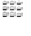
図3に、本発明の電子写真感光体の層構成の例を示す。 FIG. 3 shows an example of the layer structure of the electrophotographic photosensitive member of the present invention.
図3(a)に示される層構成の電子写真感光体は、支持体31の上に電荷発生物質を含有する層(電荷発生層)341、電荷輸送物質を含有する層(第1の電荷輸送層)342が順に設けられており、さらにその上に表面層として、連鎖重合性官能基を有する正孔輸送性化合物を重合させることによって形成した層(第2の電荷輸送層)35が設けられている。
In the electrophotographic photosensitive member having the layer structure shown in FIG. 3A, a layer (charge generation layer) 341 containing a charge generation material on a
また、図3(b)に示される層構成の電子写真感光体は、支持体31の上に電荷発生物質と電荷輸送物質とを含有する層34が設けられており、さらにその上に表面層として、連鎖重合性官能基を有する正孔輸送性化合物を重合させることによって形成した層35が設けられている。
In the electrophotographic photosensitive member having the layer structure shown in FIG. 3B, a
また、図3(c)に示される層構成の電子写真感光体は、支持体31の上に電荷発生物質を含有する層(電荷発生層)341が設けられており、その上に表面層として連鎖重合性官能基を有する正孔輸送性化合物を重合させることによって形成した層35が直接設けられている。
In addition, the electrophotographic photosensitive member having a layer structure shown in FIG. 3C is provided with a layer (charge generation layer) 341 containing a charge generation material on a
また、図3(d)〜(i)に示すように、支持体31と電荷発生物質を含有する層(電荷発生層)341または電荷発生物質と電荷輸送物質とを含有する層34との間に、バリ
ア機能や接着機能を有する中間層(「下引き層」とも呼ばれる。)33や、干渉縞防止などを目的とする導電層32などを設けてもよい。
Further, as shown in FIGS. 3D to 3I, between the
その他、どのような層構成であっても、電子写真感光体の表面のユニバーサル硬さ値(HU)および弾性変形率が上記範囲にあるようにすればよいが、電子写真感光体の表面層を連鎖重合性官能基を有する正孔輸送性化合物を重合させることによって形成した層とする場合は、図3(a)〜(i)に示される層構成のうち、図(a)、(d)、(g)で示される層構成が好ましい。 In addition, the universal hardness value (HU) and elastic deformation rate of the surface of the electrophotographic photosensitive member may be in the above ranges regardless of the layer configuration. In the case of forming a layer formed by polymerizing a hole transporting compound having a chain polymerizable functional group, among the layer configurations shown in FIGS. 3 (a) to 3 (i), FIG. , (G) is preferable.
支持体としては、導電性を示すもの(導電性支持体)であればよく、また、電子写真感光体の表面の硬度の測定に影響を与えないものであればよく、例えば、アルミニウム、銅、クロム、ニッケル、亜鉛、ステンレスなどの金属製(合金製)の支持体を用いることができる。また、アルミニウム、アルミニウム合金、酸化インジウム−酸化スズ合金などを真空蒸着によって被膜形成した層を有する上記金属製支持体やプラスチック製支持体を用いることもできる。また、カーボンブラック、酸化スズ粒子、酸化チタン粒子、銀粒子などの導電性粒子を適当な結着樹脂と共にプラスチックや紙に含浸した支持体や、導電性結着樹脂を有するプラスチック製の支持体などを用いることもできる。支持体の形状としては、円筒状、ベルト状などが挙げられるが、円筒状が好ましい。 As the support, any material may be used as long as it exhibits conductivity (conductive support), and any material that does not affect the measurement of the surface hardness of the electrophotographic photosensitive member. For example, aluminum, copper, A support made of a metal (made of alloy) such as chromium, nickel, zinc, and stainless steel can be used. Moreover, the said metal support body and plastic support body which have a layer in which aluminum, an aluminum alloy, an indium oxide tin oxide alloy etc. were formed into a film by vacuum deposition can also be used. In addition, a support in which conductive particles such as carbon black, tin oxide particles, titanium oxide particles, and silver particles are impregnated into plastic or paper together with an appropriate binder resin, or a plastic support having a conductive binder resin, etc. Can also be used. Examples of the shape of the support include a cylindrical shape and a belt shape, and a cylindrical shape is preferable.
また、支持体の表面は、レーザー光などの散乱による干渉縞の防止などを目的として、切削処理、粗面化処理、アルマイト処理などを施してもよい。 The surface of the support may be subjected to cutting treatment, roughening treatment, alumite treatment, etc. for the purpose of preventing interference fringes due to scattering of laser light or the like.
上述のとおり、支持体と感光層(電荷発生層、電荷輸送層)または後述の中間層との間には、レーザー光などの散乱による干渉縞の防止や、支持体の傷の被覆を目的とした導電層を設けてもよい。 As described above, between the support and the photosensitive layer (charge generation layer, charge transport layer) or an intermediate layer described later, for the purpose of preventing interference fringes due to scattering of laser light or the like and covering the scratches on the support An electrically conductive layer may be provided.
導電層は、カーボンブラック、金属粒子、金属酸化物粒子などの導電性粒子を結着樹脂に分散させて形成することができる。 The conductive layer can be formed by dispersing conductive particles such as carbon black, metal particles, and metal oxide particles in a binder resin.
導電層の膜厚は、1〜40μmであることが好ましく、特には2〜20μmであることがより好ましい。 The thickness of the conductive layer is preferably 1 to 40 μm, and more preferably 2 to 20 μm.
また、上述のとおり、支持体または導電層と感光層(電荷発生層、電荷輸送層)との間には、バリア機能や接着機能を有する中間層を設けてもよい。中間層は、感光層の接着性改良、塗工性改良、支持体からの電荷注入性改良、感光層の電気的破壊に対する保護などのために形成される。 Further, as described above, an intermediate layer having a barrier function or an adhesive function may be provided between the support or the conductive layer and the photosensitive layer (charge generation layer, charge transport layer). The intermediate layer is formed for the purpose of improving the adhesion of the photosensitive layer, improving the coating property, improving the charge injection property from the support, and protecting the photosensitive layer from electrical breakdown.
中間層は、ポリビニルアルコール、ポリ−N−ビニルイミダゾール、ポリエチレンオキシド、エチルセルロース、エチレン−アクリル酸共重合体、カゼイン、ポリアミド、N−メトキシメチル化6ナイロン、共重合ナイロン、にかわ、ゼラチンなどの材料を用いて形成することができる。 The intermediate layer is made of materials such as polyvinyl alcohol, poly-N-vinylimidazole, polyethylene oxide, ethyl cellulose, ethylene-acrylic acid copolymer, casein, polyamide, N-methoxymethylated 6 nylon, copolymer nylon, glue and gelatin. Can be formed.
中間層の膜厚は0.1〜2μmであることが好ましい。 The film thickness of the intermediate layer is preferably 0.1 to 2 μm.
本発明の電子写真感光体に用いられる電荷発生物質としては、例えば、セレン−テルル、ピリリウム、チアピリリウム系染料、各種の中心金属および各種の結晶系(α、β、γ、ε、X型など)を有するフタロシアニン顔料や、アントアントロン顔料や、ジベンズピレンキノン顔料や、ピラントロン顔料や、モノアゾ、ジスアゾ、トリスアゾなどのアゾ顔料や、インジゴ顔料や、キナクリドン顔料や、非対称キノシアニン顔料や、キノシアニン顔料や、アモルファスシリコン(特開昭54−143645号公報などに記載)などが挙
げられる。これら電荷発生物質は1種のみ用いてもよく、2種以上用いてもよい。
Examples of the charge generating material used in the electrophotographic photosensitive member of the present invention include selenium-tellurium, pyrylium, thiapyrylium dyes, various central metals, and various crystal systems (α, β, γ, ε, X type, etc.). Phthalocyanine pigments, anthanthrone pigments, dibenzpyrenequinone pigments, pyrantron pigments, azo pigments such as monoazo, disazo, trisazo, indigo pigments, quinacridone pigments, asymmetric quinocyanine pigments, quinocyanine pigments, Examples thereof include amorphous silicon (described in JP-A No. 54-143645). These charge generation materials may be used alone or in combination of two or more.
本発明の電子写真感光体に用いられる電荷輸送物質としては、上記の連鎖重合性官能基を有する正孔輸送性化合物以外に、例えば、ポリ−N−ビニルカルバゾール、ポリスチリルアントラセンなどの複素環や縮合多環芳香族を有する高分子化合物や、ピラゾリン、イミダゾール、オキサゾール、トリアゾール、カルバゾールなどの複素環化合物や、トリフェニルメタンなどのトリアリールアルカン誘導体や、トリフェニルアミンなどのトリアリールアミン誘導体や、フェニレンジアミン誘導体や、N−フェニルカルバゾール誘導体や、スチルベン誘導体や、ヒドラゾン誘導体などが挙げられる。 As the charge transport material used in the electrophotographic photoreceptor of the present invention, in addition to the hole transport compound having the chain polymerizable functional group, for example, a heterocyclic ring such as poly-N-vinylcarbazole and polystyrylanthracene, Polymer compounds having condensed polycyclic aromatics, heterocyclic compounds such as pyrazoline, imidazole, oxazole, triazole, carbazole, triarylalkane derivatives such as triphenylmethane, triarylamine derivatives such as triphenylamine, Examples include phenylenediamine derivatives, N-phenylcarbazole derivatives, stilbene derivatives, hydrazone derivatives, and the like.
感光層を電荷発生層と電荷輸送層とに機能分離する場合、電荷発生層は、電荷発生物質を結着樹脂および溶剤と共に分散して得られる電荷発生層用塗布液を塗布し、乾燥することによって形成することができる。分散方法としては、ホモジナイザー、超音波分散機、ボールミル、振動ボールミル、サンドミル、ロールミル、アトライター、液衝突型高速分散機などを用いた方法が挙げられる。電荷発生物質と結着樹脂との割合は、1:0.3〜1:4(質量比)の範囲が好ましい。また、上記電荷発生物質を単独で蒸着法などにより成膜し、電荷発生層とすることもできる。 When the photosensitive layer is functionally separated into a charge generation layer and a charge transport layer, the charge generation layer is coated with a coating solution for a charge generation layer obtained by dispersing a charge generation material together with a binder resin and a solvent, and dried. Can be formed. Examples of the dispersion method include a method using a homogenizer, an ultrasonic disperser, a ball mill, a vibrating ball mill, a sand mill, a roll mill, an attritor, a liquid collision type high-speed disperser, and the like. The ratio between the charge generating material and the binder resin is preferably in the range of 1: 0.3 to 1: 4 (mass ratio). Alternatively, the charge generation material can be formed alone by a vapor deposition method or the like to form a charge generation layer.
電荷発生層の膜厚は5μm以下であることが好ましく、特には0.1〜2μmであることがより好ましい。 The thickness of the charge generation layer is preferably 5 μm or less, and more preferably 0.1 to 2 μm.
感光層を電荷発生層と電荷輸送層とに機能分離する場合、電荷輸送層、特に電子写真感光体の表面層でない電荷輸送層は、電荷輸送物質と結着樹脂を溶剤に溶解して得られる電荷輸送層用塗布液を塗布し、乾燥することによって形成することができる。また、上記電荷輸送物質のうち単独で成膜性を有するものは、結着樹脂を用いずにそれ単独で成膜し、電荷輸送層とすることもできる。電荷輸送物質と結着樹脂との割合は、2:8〜10:0(質量比)の範囲が好ましく、特には3:7〜10:0(質量比)の範囲がより好ましい。電荷輸送物質の量が少なすぎると、電荷輸送能が低下し、感度低下や残留電位上昇が生じる場合がある。 When the photosensitive layer is functionally separated into a charge generation layer and a charge transport layer, a charge transport layer, particularly a charge transport layer that is not a surface layer of an electrophotographic photosensitive member, is obtained by dissolving a charge transport material and a binder resin in a solvent. It can form by apply | coating the coating liquid for charge transport layers, and drying. In addition, among the above charge transport materials, those having film formability alone can be formed as a charge transport layer by itself without using a binder resin. The ratio between the charge transport material and the binder resin is preferably in the range of 2: 8 to 10: 0 (mass ratio), and more preferably in the range of 3: 7 to 10: 0 (mass ratio). If the amount of the charge transporting material is too small, the charge transporting ability is lowered, and the sensitivity may be lowered or the residual potential may be raised.
電荷輸送層、特に電子写真感光体の表面層でない電荷輸送層の膜厚は1〜50μmであることが好ましく、1〜30μmであることがより好ましく、3〜30μmであることがより好ましく、3〜20μmであることがより好ましい。 The film thickness of the charge transport layer, particularly the charge transport layer that is not the surface layer of the electrophotographic photosensitive member, is preferably 1 to 50 μm, more preferably 1 to 30 μm, and more preferably 3 to 30 μm. More preferably, it is ˜20 μm.
電荷輸送物質と電荷発生物質を同一の層に含有させる場合、該層は、上記電荷発生物質および上記電荷輸送物質を結着樹脂および溶剤と共に分散して得られる該層用の塗布液を塗布し、乾燥することによって形成することができる。 When the charge transport material and the charge generation material are contained in the same layer, the layer is coated with a coating solution for the layer obtained by dispersing the charge generation material and the charge transport material together with a binder resin and a solvent. It can be formed by drying.
感光層(電荷輸送層、電荷発生層)に用いられる結着樹脂としては、例えば、スチレン、酢酸ビニル、塩化ビニル、アクリル酸エステル、メタクリル酸エステル、フッ化ビニリデン、トリフルオロエチレンなどのビニル化合物の重合体または共重合体や、ポリビニルアルコール樹脂や、ポリビニルアセタール樹脂や、ポリビニルブチラール樹脂や、ポリカーボネート樹脂や、ポリアリレート樹脂や、ポリエステル樹脂や、ポリスルホン樹脂や、ポリフェニレンオキサイド樹脂や、ポリウレタン樹脂や、セルロース樹脂や、フェノール樹脂や、メラミン樹脂や、ケイ素樹脂や、エポキシ樹脂などが挙げられる。これらは単独、混合または共重合体として1種または2種以上用いることができる。 Examples of the binder resin used in the photosensitive layer (charge transport layer, charge generation layer) include vinyl compounds such as styrene, vinyl acetate, vinyl chloride, acrylate ester, methacrylate ester, vinylidene fluoride, and trifluoroethylene. Polymer or copolymer, polyvinyl alcohol resin, polyvinyl acetal resin, polyvinyl butyral resin, polycarbonate resin, polyarylate resin, polyester resin, polysulfone resin, polyphenylene oxide resin, polyurethane resin, cellulose Resins, phenol resins, melamine resins, silicon resins, epoxy resins, and the like can be given. These can be used singly or in combination of two or more as a mixture or copolymer.
図4に、本発明の電子写真感光体を有するプロセスカートリッジを備えた電子写真装置の概略構成の一例を示す。 FIG. 4 shows an example of a schematic configuration of an electrophotographic apparatus provided with a process cartridge having the electrophotographic photosensitive member of the present invention.
図4において、1は円筒状の電子写真感光体であり、軸2を中心に矢印方向に所定の周速度で回転駆動される。
In FIG. 4,
回転駆動される電子写真感光体1の表面は、帯電手段(一次帯電手段:帯電ローラーなど)3により、正または負の所定電位に均一に帯電され、次いで、スリット露光やレーザービーム走査露光などの露光手段(不図示)から出力される露光光(画像露光光)4を受ける。こうして電子写真感光体1の表面に、目的の画像に対応した静電潜像が順次形成されていく。
The surface of the electrophotographic
電子写真感光体1の表面に形成された静電潜像は、現像手段5の現像剤に含まれるトナーにより現像されてトナー像となる。次いで、電子写真感光体1の表面に形成担持されているトナー像が、転写手段(転写ローラーなど)6からの転写バイアスによって、転写材供給手段(不図示)から電子写真感光体1と転写手段6との間(当接部)に電子写真感光体1の回転と同期して取り出されて給送された転写材(紙など)Pに順次転写されていく。
The electrostatic latent image formed on the surface of the
トナー像の転写を受けた転写材Pは、電子写真感光体1の表面から分離されて定着手段8へ導入されて像定着を受けることにより画像形成物(プリント、コピー)として装置外へプリントアウトされる。
The transfer material P that has received the transfer of the toner image is separated from the surface of the electrophotographic
トナー像転写後の電子写真感光体1の表面は、クリーニング手段(クリーニングブレードなど)7によって転写残りの現像剤(トナー)の除去を受けて清浄面化され、さらに前露光手段(不図示)からの前露光光(不図示)により除電処理された後、繰り返し画像形成に使用される。なお、図4に示すように、帯電手段3が帯電ローラーなどを用いた接触帯電手段である場合は、前露光は必ずしも必要ではない。
The surface of the electrophotographic
上述の電子写真感光体1、帯電手段3、現像手段5、転写手段6およびクリーニング手段7などの構成要素のうち、複数のものを容器に納めてプロセスカートリッジとして一体に結合して構成し、このプロセスカートリッジを複写機やレーザービームプリンターなどの電子写真装置本体に対して着脱自在に構成してもよい。図4では、電子写真感光体1と、帯電手段3、現像手段5およびクリーニング手段7とを一体に支持してカートリッジ化して、電子写真装置本体のレールなどの案内手段10を用いて電子写真装置本体に着脱自在なプロセスカートリッジ9としている。
Among the above-described components such as the electrophotographic
以下に、具体的な実施例を挙げて本発明をさらに詳細に説明する。ただし、本発明はこれらに限定されるものではない。なお、実施例中の「部」は「質量部」を意味する。また、実施例7〜13、15および18は参考例である。 Hereinafter, the present invention will be described in more detail with reference to specific examples. However, the present invention is not limited to these. In the examples, “part” means “part by mass”. Examples 7 to 13, 15 and 18 are reference examples.
(実施例1) (Example 1)
直径30mm、長さ357.5mmのアルミニウムシリンダーの表面をホーニング処理
し、超音波洗浄したものを支持体とした。
The surface of an aluminum cylinder having a diameter of 30 mm and a length of 357.5 mm was subjected to honing treatment and subjected to ultrasonic cleaning as a support.
次に、N−メトキシメチル化6ナイロン5部を、メタノール95部に溶解して、中間層用塗布液を調製した。 Next, 5 parts of N-methoxymethylated 6 nylon was dissolved in 95 parts of methanol to prepare an intermediate layer coating solution.
この中間層用塗布液を、支持体上に浸漬塗布し、100℃で20分間乾燥して、膜厚が0.6μmの中間層を形成した。 This intermediate layer coating solution was dip coated on the support and dried at 100 ° C. for 20 minutes to form an intermediate layer having a thickness of 0.6 μm.
次に、CuKα特性X線回折におけるブラッグ角2θ±0.2°の9.0°、14.2
°、23.9°および27.1°に強いピークを有するオキシチタニウムフタロシアニン結晶(電荷発生物質)3部、ポリビニルブチラール樹脂(商品名:エスレックBM2、積水化学(株)製)3部、および、シクロヘキサノン35部を、直径1mmのガラスビーズを用いたサンドミル装置で2時間分散した後、これに酢酸エチル60部を加えて、電荷発生層用塗布液を調製した。
Next, the Bragg angle 2θ ± 0.2 ° in CuKα characteristic X-ray diffraction is 9.0 °, 14.2
3 parts of oxytitanium phthalocyanine crystal (charge generation material) having strong peaks at °, 23.9 ° and 27.1 °, 3 parts of polyvinyl butyral resin (trade name: ESREC BM2, manufactured by Sekisui Chemical Co., Ltd.), and After 35 parts of cyclohexanone was dispersed in a sand mill using glass beads having a diameter of 1 mm for 2 hours, 60 parts of ethyl acetate was added thereto to prepare a charge generation layer coating solution.
この電荷発生層用塗布液を、中間層上に浸漬塗布し、50℃で10分間乾燥して、膜厚が0.2μmの電荷発生層を形成した。 This charge generation layer coating solution was dip-coated on the intermediate layer and dried at 50 ° C. for 10 minutes to form a charge generation layer having a thickness of 0.2 μm.
次に、下記式(E−1)で示される構造を有する正孔輸送性化合物60部を、モノクロロベンゼン30部/ジクロロメタン30部の混合溶剤に溶解して、電荷輸送層用塗布液を調製した。 Next, 60 parts of a hole transporting compound having a structure represented by the following formula (E-1) was dissolved in a mixed solvent of 30 parts of monochlorobenzene / 30 parts of dichloromethane to prepare a coating solution for a charge transport layer. .
この電荷輸送層用塗布液を、電荷発生層上に浸漬塗布した。 This charge transport layer coating solution was dip coated on the charge generation layer.
次に、電荷発生層上に塗布した電荷輸送層用塗布液に、酸素濃度10ppmの雰囲気下で加速電圧150kV、照射線量4Mradの条件で電子線を照射し、その後、同雰囲気下で電子写真感光体(=電子線の被照射体)の温度が100℃になる条件で10分間加熱処理を行い、膜厚15μmの電荷輸送層を形成した。 Next, the charge transport layer coating solution applied on the charge generation layer is irradiated with an electron beam in an atmosphere having an oxygen concentration of 10 ppm under the conditions of an acceleration voltage of 150 kV and an irradiation dose of 4 Mrad. Heat treatment was performed for 10 minutes under the condition that the temperature of the body (= electron beam irradiated body) was 100 ° C., and a charge transport layer having a thickness of 15 μm was formed.
このようにして実施例1の表面物性測定用(ユニバーサル硬さ値(HU)・弾性変形率測定用)の電子写真感光体を作製した。 In this way, an electrophotographic photosensitive member for measuring surface physical properties (for universal hardness value (HU) / elastic deformation rate measurement) of Example 1 was produced.
また、上記と全く同様にしてもう1つ電子写真感光体を作製し、これを実施例1の実機試験用の電子写真感光体とした。 Further, another electrophotographic photosensitive member was produced in the same manner as described above, and this was used as an electrophotographic photosensitive member for actual machine testing of Example 1.
・ユニバーサル硬さ値(HU)および弾性変形率の測定
表面物性測定用の電子写真感光体を25℃/50%RH環境下に24時間放置した後、上述のFischer社製フィシャースコープH100Vを用いて、上述のとおり、ユニバーサル硬さ値(HU)および弾性変形率の測定を行った。ユニバーサル硬さ値(HU)および弾性変形率の測定結果を表1に示す。
Measurement of universal hardness value (HU) and elastic deformation rate After leaving an electrophotographic photosensitive member for measuring surface physical properties in a 25 ° C./50% RH environment for 24 hours, the above Fischer scope H100V manufactured by Fischer was used. As described above, the universal hardness value (HU) and elastic deformation rate were measured. Table 1 shows the measurement results of universal hardness value (HU) and elastic deformation rate.
・実機試験
常温常湿(23℃/50%RH)環境下、実機試験用の電子写真感光体をキヤノン(株)製複写機GP40に装着して、初期の出力画像の評価を行った。次に、40000枚通紙耐久試験を行い、出力画像の評価および耐久試験後の電子写真感光体の削れ量を測定した。削れ量の測定には、渦電流式膜厚計PERMASCOPE TYPE E111(Fischer社製)を使用した。なお、耐久試験は、プリント1枚ごとに1回停止する間欠モードで行った。実機試験の評価結果を表1に示す。
-Actual machine test In an environment of normal temperature and normal humidity (23 ° C / 50% RH), an electrophotographic photosensitive member for actual machine test was mounted on a copying machine GP40 manufactured by Canon Inc., and an initial output image was evaluated. Next, a 40,000 sheet passing durability test was performed, and the amount of abrasion of the electrophotographic photosensitive member after the evaluation of the output image and the durability test was measured. An eddy current film thickness meter PERMASCOPE TYPE E111 (manufactured by Fischer) was used for measurement of the amount of scraping. The durability test was performed in an intermittent mode in which the print was stopped once for each print. Table 1 shows the evaluation results of the actual machine test.
(実施例2)
実施例1において、電荷輸送層用塗布液に電子線を照射する際の照射線量を4Mradから8Mradに変更した以外は、実施例1と同様にして表面物性測定用の電子写真感光体および実機試験用の電子写真感光体を作製し、また、実施例1と同様にして、ユニバーサル硬さ値(HU)および弾性変形率の測定ならびに実機試験を行った。ユニバーサル硬
さ値(HU)および弾性変形率の測定結果ならびに実機試験の評価結果を表1に示す。
(Example 2)
In Example 1, an electrophotographic photoreceptor for measuring surface physical properties and an actual machine test were carried out in the same manner as in Example 1 except that the irradiation dose for irradiating the coating solution for charge transport layer with an electron beam was changed from 4 Mrad to 8 Mrad. An electrophotographic photosensitive member was prepared, and in the same manner as in Example 1, measurement of universal hardness value (HU) and elastic deformation rate and actual machine test were performed. Table 1 shows the measurement results of the universal hardness value (HU) and elastic deformation rate, and the evaluation results of the actual machine test.
(実施例3)
実施例1において、電荷輸送層用塗布液に電子線を照射する際の照射線量を4Mradから20Mradに変更した以外は、実施例1と同様にして表面物性測定用の電子写真感光体および実機試験用の電子写真感光体を作製し、また、実施例1と同様にして、ユニバーサル硬さ値(HU)および弾性変形率の測定ならびに実機試験を行った。ユニバーサル硬さ値(HU)および弾性変形率の測定結果ならびに実機試験の評価結果を表1に示す。
(Example 3)
In Example 1, an electrophotographic photoreceptor for measuring surface physical properties and an actual machine test were carried out in the same manner as in Example 1 except that the irradiation dose when irradiating the coating solution for charge transport layer with an electron beam was changed from 4 Mrad to 20 Mrad. An electrophotographic photosensitive member was prepared, and in the same manner as in Example 1, measurement of universal hardness value (HU) and elastic deformation rate and actual machine test were performed. Table 1 shows the measurement results of the universal hardness value (HU) and elastic deformation rate, and the evaluation results of the actual machine test.
(実施例4)
実施例1と同様にして、支持体上に中間層および電荷発生層を形成した。
次に、下記式(E−2)で示される構造を有するスチリル化合物10部、および、下記式(E−3)で示される繰り返し構造単位を有するポリカーボネート樹脂(粘度平均分子量(Mv):20000)10部を、モノクロロベンゼン50部/ジクロロメタン30部の混合溶剤に溶解して、第1電荷輸送層用塗布液を調製した。
Example 4
In the same manner as in Example 1, an intermediate layer and a charge generation layer were formed on the support.
Next, 10 parts of a styryl compound having a structure represented by the following formula (E-2) and a polycarbonate resin having a repeating structural unit represented by the following formula (E-3) (viscosity average molecular weight (Mv): 20000) 10 parts were dissolved in a mixed solvent of 50 parts of monochlorobenzene / 30 parts of dichloromethane to prepare a coating solution for the first charge transport layer.
この第1電荷輸送層用塗布液を、電荷発生層上に浸漬塗布し、120℃で1時間乾燥して、膜厚が20μmの第1電荷輸送層を形成した。 This first charge transport layer coating solution was dip-coated on the charge generation layer and dried at 120 ° C. for 1 hour to form a first charge transport layer having a thickness of 20 μm.
次に、上記式(E−1)で示される構造を有する正孔輸送性化合物60部を、モノクロロベンゼン50部/ジクロロメタン50部の混合溶剤に溶解して、第2電荷輸送層用塗布液を調製した。
この第2電荷輸送層用塗布液を、第1電荷輸送層上にスプレーコーティングした。
Next, 60 parts of the hole transporting compound having the structure represented by the above formula (E-1) is dissolved in a mixed solvent of 50 parts of monochlorobenzene / 50 parts of dichloromethane to obtain a coating solution for the second charge transporting layer. Prepared.
The coating solution for the second charge transport layer was spray-coated on the first charge transport layer.
次に、第1電荷輸送層層上に塗布した第2電荷輸送層用塗布液に、酸素濃度10ppmの雰囲気下で加速電圧150kV、照射線量4Mradの条件で電子線を照射し、その後、同雰囲気下で電子写真感光体(=電子線の被照射体)の温度が100℃になる条件で10分間加熱処理を行い、膜厚5μmの第2電荷輸送層を形成した。
このようにして実施例4の表面物性測定用の電子写真感光体を作製した。
Next, the second charge transport layer coating solution coated on the first charge transport layer is irradiated with an electron beam under the conditions of an acceleration voltage of 150 kV and an irradiation dose of 4 Mrad in an atmosphere having an oxygen concentration of 10 ppm. Under the condition that the temperature of the electrophotographic photosensitive member (= electron beam irradiated body) was 100 ° C., a heat treatment was performed for 10 minutes to form a second charge transport layer having a thickness of 5 μm.
Thus, an electrophotographic photosensitive member for measuring surface physical properties of Example 4 was produced.
また、上記と全く同様にしてもう1つ電子写真感光体を作製し、これを実施例4の実機試験用の電子写真感光体とした。
実施例4の表面物性測定用の電子写真感光体について、実施例1と同様にしてユニバーサル硬さ値(HU)および弾性変形率の測定を行い、また、実施例4の実機試験用の電子写真感光体について、実施例1と同様にして実機試験を行った。ユニバーサル硬さ値(HU)および弾性変形率の測定結果ならびに実機試験の評価結果を表1に示す。
Further, another electrophotographic photosensitive member was produced in the same manner as described above, and this was used as an electrophotographic photosensitive member for actual machine testing of Example 4.
For the electrophotographic photosensitive member for measuring the surface physical properties of Example 4, the universal hardness value (HU) and the elastic deformation rate were measured in the same manner as in Example 1, and the electrophotographic for actual machine test of Example 4 was performed. The photoconductor was tested in the same manner as in Example 1. Table 1 shows the measurement results of the universal hardness value (HU) and elastic deformation rate, and the evaluation results of the actual machine test.
(実施例5)
実施例4において、第2電荷輸送層用塗布液に電子線を照射する際の照射線量を4Mradから8Mradに変更した以外は、実施例4と同様にして表面物性測定用の電子写真感光体および実機試験用の電子写真感光体を作製し、また、実施例4と同様にして、ユニバーサル硬さ値(HU)および弾性変形率の測定ならびに実機試験を行った。ユニバーサル硬さ値(HU)および弾性変形率の測定結果ならびに実機試験の評価結果を表1に示す。
(Example 5)
In Example 4, an electrophotographic photosensitive member for measuring surface physical properties was obtained in the same manner as in Example 4 except that the irradiation dose when irradiating the coating solution for the second charge transport layer with an electron beam was changed from 4 Mrad to 8 Mrad. An electrophotographic photosensitive member for an actual machine test was produced, and the universal hardness value (HU) and the elastic deformation rate were measured and the actual machine test was performed in the same manner as in Example 4. Table 1 shows the measurement results of the universal hardness value (HU) and elastic deformation rate, and the evaluation results of the actual machine test.
(実施例6)
実施例4において、第2電荷輸送層用塗布液に電子線を照射する際の照射線量を4Mradから20Mradに変更した以外は、実施例4と同様にして表面物性測定用の電子写真感光体および実機試験用の電子写真感光体を作製し、また、実施例4と同様にして、ユニバーサル硬さ値(HU)および弾性変形率の測定ならびに実機試験を行った。ユニバーサル硬さ値(HU)および弾性変形率の測定結果ならびに実機試験の評価結果を表1に示す。
(Example 6)
In Example 4, an electrophotographic photosensitive member for measuring surface physical properties was obtained in the same manner as in Example 4 except that the irradiation dose when irradiating the coating solution for the second charge transport layer with an electron beam was changed from 4 Mrad to 20 Mrad. An electrophotographic photosensitive member for an actual machine test was produced, and the universal hardness value (HU) and the elastic deformation rate were measured and the actual machine test was performed in the same manner as in Example 4. Table 1 shows the measurement results of the universal hardness value (HU) and elastic deformation rate, and the evaluation results of the actual machine test.
(実施例7)
実施例1において、電荷輸送層に用いた正孔輸送性化合物を上記式(E−1)で示される構造を有する正孔輸送性化合物から下記式(E−4)で示される構造を有する正孔輸送性化合物に変更した以外は、実施例1と同様にして表面物性測定用の電子写真感光体および実機試験用の電子写真感光体を作製し、また、実施例1と同様にして、ユニバーサル硬さ値(HU)および弾性変形率の測定ならびに実機試験を行った。ユニバーサル硬さ値(HU)および弾性変形率の測定結果ならびに実機試験の評価結果を表1に示す。
(Example 7)
In Example 1, the hole transporting compound used for the charge transporting layer was changed from the hole transporting compound having the structure represented by the above formula (E-1) to the positive compound having the structure represented by the following formula (E-4). An electrophotographic photosensitive member for measuring surface physical properties and an electrophotographic photosensitive member for testing an actual machine were prepared in the same manner as in Example 1 except that the compound was changed to a hole-transporting compound. Measurement of hardness value (HU) and elastic deformation rate and actual machine test were performed. Table 1 shows the measurement results of the universal hardness value (HU) and elastic deformation rate, and the evaluation results of the actual machine test.
(実施例8)
実施例2において、電荷輸送層に用いた正孔輸送性化合物を上記式(E−1)で示される構造を有する正孔輸送性化合物から上記式(E−4)で示される構造を有する正孔輸送性化合物に変更した以外は、実施例2と同様にして表面物性測定用の電子写真感光体および実機試験用の電子写真感光体を作製し、また、実施例2と同様にして、ユニバーサル硬さ値(HU)および弾性変形率の測定ならびに実機試験を行った。ユニバーサル硬さ値(HU)および弾性変形率の測定結果ならびに実機試験の評価結果を表1に示す。
(Example 8)
In Example 2, the hole transporting compound used for the charge transporting layer was changed from the hole transporting compound having the structure represented by the above formula (E-1) to the positive compound having the structure represented by the above formula (E-4). An electrophotographic photosensitive member for measuring surface physical properties and an electrophotographic photosensitive member for testing an actual machine were prepared in the same manner as in Example 2 except that the compound was changed to a hole-transporting compound. Measurement of hardness value (HU) and elastic deformation rate and actual machine test were performed. Table 1 shows the measurement results of the universal hardness value (HU) and elastic deformation rate, and the evaluation results of the actual machine test.
(実施例9)
実施例3において、電荷輸送層に用いた正孔輸送性化合物を上記式(E−1)で示される構造を有する正孔輸送性化合物から上記式(E−4)で示される構造を有する正孔輸送性化合物に変更した以外は、実施例3と同様にして表面物性測定用の電子写真感光体および実機試験用の電子写真感光体を作製し、また、実施例3と同様にして、ユニバーサル硬さ値(HU)および弾性変形率の測定ならびに実機試験を行った。ユニバーサル硬さ値(HU)および弾性変形率の測定結果ならびに実機試験の評価結果を表1に示す。
Example 9
In Example 3, the hole transporting compound used in the charge transporting layer was changed from the hole transporting compound having the structure represented by the above formula (E-1) to the positive compound having the structure represented by the above formula (E-4). An electrophotographic photosensitive member for measuring surface physical properties and an electrophotographic photosensitive member for testing an actual machine were prepared in the same manner as in Example 3 except that the compound was changed to a hole-transporting compound. Measurement of hardness value (HU) and elastic deformation rate and actual machine test were performed. Table 1 shows the measurement results of the universal hardness value (HU) and elastic deformation rate, and the evaluation results of the actual machine test.
(実施例10)
実施例1において、電荷輸送層に用いた正孔輸送性化合物を上記式(E−1)で示される構造を有する正孔輸送性化合物から下記式(E−5)で示される構造を有する正孔輸送性化合物に変更した以外は、実施例1と同様にして表面物性測定用の電子写真感光体および実機試験用の電子写真感光体を作製し、また、実施例1と同様にして、ユニバーサル硬さ値(HU)および弾性変形率の測定ならびに実機試験を行った。ユニバーサル硬さ値(HU)および弾性変形率の測定結果ならびに実機試験の評価結果を表1に示す。
(Example 10)
In Example 1, the hole transporting compound used for the charge transporting layer was changed from the hole transporting compound having the structure represented by the above formula (E-1) to the positive compound having the structure represented by the following formula (E-5). An electrophotographic photosensitive member for measuring surface physical properties and an electrophotographic photosensitive member for testing an actual machine were prepared in the same manner as in Example 1 except that the compound was changed to a hole-transporting compound. Measurement of hardness value (HU) and elastic deformation rate and actual machine test were performed. Table 1 shows the measurement results of the universal hardness value (HU) and elastic deformation rate, and the evaluation results of the actual machine test.
(実施例11)
実施例1において、電荷輸送層に用いた正孔輸送性化合物を上記式(E−1)で示される構造を有する正孔輸送性化合物から下記式(E−6)で示される構造を有する正孔輸送性化合物に変更した以外は、実施例1と同様にして表面物性測定用の電子写真感光体および実機試験用の電子写真感光体を作製し、また、実施例1と同様にして、ユニバーサル硬さ値(HU)および弾性変形率の測定ならびに実機試験を行った。ユニバーサル硬さ値(HU)および弾性変形率の測定結果ならびに実機試験の評価結果を表1に示す。
(Example 11)
In Example 1, the hole transporting compound used for the charge transporting layer was changed from the hole transporting compound having the structure represented by the above formula (E-1) to the positive compound having the structure represented by the following formula (E-6). An electrophotographic photosensitive member for measuring surface physical properties and an electrophotographic photosensitive member for testing an actual machine were prepared in the same manner as in Example 1 except that the compound was changed to a hole-transporting compound. Measurement of hardness value (HU) and elastic deformation rate and actual machine test were performed. Table 1 shows the measurement results of the universal hardness value (HU) and elastic deformation rate, and the evaluation results of the actual machine test.
(実施例12)
実施例1において、電荷輸送層に用いた正孔輸送性化合物を上記式(E−1)で示される構造を有する正孔輸送性化合物から下記式(E−7)で示される構造を有する正孔輸送性化合物に変更した以外は、実施例1と同様にして表面物性測定用の電子写真感光体および実機試験用の電子写真感光体を作製し、また、実施例1と同様にして、ユニバーサル硬さ値(HU)および弾性変形率の測定ならびに実機試験を行った。ユニバーサル硬さ値(HU)および弾性変形率の測定結果ならびに実機試験の評価結果を表1に示す。
Example 12
In Example 1, the hole transporting compound used for the charge transporting layer was changed from the hole transporting compound having the structure represented by the above formula (E-1) to the positive compound having the structure represented by the following formula (E-7). An electrophotographic photosensitive member for measuring surface physical properties and an electrophotographic photosensitive member for testing an actual machine were prepared in the same manner as in Example 1 except that the compound was changed to a hole-transporting compound. Measurement of hardness value (HU) and elastic deformation rate and actual machine test were performed. Table 1 shows the measurement results of the universal hardness value (HU) and elastic deformation rate, and the evaluation results of the actual machine test.
(実施例13)
実施例7において、電荷輸送層用塗布液を以下のように調製したものに変更した以外は、実施例7と同様にして表面物性測定用の電子写真感光体および実機試験用の電子写真感光体を作製し、また、実施例7と同様にして、ユニバーサル硬さ値(HU)および弾性変形率の測定ならびに実機試験を行った。ユニバーサル硬さ値(HU)および弾性変形率の測定結果ならびに実機試験の評価結果を表1に示す。
(Example 13)
In Example 7, the electrophotographic photosensitive member for surface property measurement and the electrophotographic photosensitive member for actual machine test were used in the same manner as in Example 7 except that the coating solution for charge transport layer was changed to the one prepared as follows. Further, in the same manner as in Example 7, the universal hardness value (HU) and the elastic deformation rate were measured, and the actual machine test was performed. Table 1 shows the measurement results of the universal hardness value (HU) and elastic deformation rate, and the evaluation results of the actual machine test.
すなわち、上記式(E−4)で示される構造を有する正孔輸送性化合物40部、および、下記式(E−8)で示される構造を有する正孔輸送性化合物20部を、モノクロロベンゼン50部/ジクロロメタン50部の混合溶剤に溶解して、実施例13の電荷輸送層用塗布液を調製した。 That is, 40 parts of a hole transporting compound having a structure represented by the above formula (E-4) and 20 parts of a hole transporting compound having a structure represented by the following formula (E-8) were mixed with monochlorobenzene 50. Part / dichloromethane in a mixed solvent of 50 parts to prepare a charge transport layer coating solution of Example 13.
(実施例14)
実施例1において、電荷輸送層用塗布液を以下のように調製したものに変更した以外は、実施例1と同様にして表面物性測定用の電子写真感光体および実機試験用の電子写真感光体を作製し、また、実施例1と同様にして、ユニバーサル硬さ値(HU)および弾性変形率の測定ならびに実機試験を行った。ユニバーサル硬さ値(HU)および弾性変形率の測定結果ならびに実機試験の評価結果を表1に示す。
(Example 14)
In Example 1, except that the coating solution for charge transport layer was changed to the one prepared as follows, an electrophotographic photosensitive member for measuring surface physical properties and an electrophotographic photosensitive member for testing an actual machine were the same as in Example 1. Further, in the same manner as in Example 1, the universal hardness value (HU) and the elastic deformation rate were measured, and the actual machine test was performed. Table 1 shows the measurement results of the universal hardness value (HU) and elastic deformation rate, and the evaluation results of the actual machine test.
すなわち、まず、ポリテトラフルオロエチレン樹脂粒子(商品名:ルブロンL−2、ダイキン工業(株)製)5部およびモノクロロベンゼン50部を、ガラスビーズを用いたサンドミル装置で分散した。これに、上記式(E−1)で示される構造を有する正孔輸送性化合物60部およびジクロロメタン50部を加えて、上記式(E−1)で示される構造を有する正孔輸送性化合物を溶解した後、さらにジクロロメタン30部を加えて、実施例14の電荷輸送層用塗布液を調製した。 That is, first, 5 parts of polytetrafluoroethylene resin particles (trade name: Lubron L-2, manufactured by Daikin Industries, Ltd.) and 50 parts of monochlorobenzene were dispersed in a sand mill apparatus using glass beads. To this, 60 parts of a hole transporting compound having a structure represented by the above formula (E-1) and 50 parts of dichloromethane are added, and a hole transporting compound having a structure represented by the above formula (E-1) is obtained. After dissolution, 30 parts of dichloromethane was further added to prepare a charge transport layer coating solution of Example 14.
(実施例15)
実施例4において、第2電荷輸送層用塗布液に電子線を照射した後、加熱処理を行う際の「電子写真感光体の温度が100℃になる条件」を「電子写真感光体の温度が70℃になる条件」に変更した以外は、実施例4と同様にして表面物性測定用の電子写真感光体および実機試験用の電子写真感光体を作製し、また、実施例4と同様にして、ユニバーサル硬さ値(HU)および弾性変形率の測定ならびに実機試験を行った。ユニバーサル硬さ値(HU)および弾性変形率の測定結果ならびに実機試験の評価結果を表2に示す。
(Example 15)
In Example 4, after irradiating the coating solution for the second charge transport layer with an electron beam, the “condition for the temperature of the electrophotographic photosensitive member to be 100 ° C.” when performing the heat treatment is “the temperature of the electrophotographic photosensitive member is An electrophotographic photosensitive member for measuring surface physical properties and an electrophotographic photosensitive member for actual machine testing were prepared in the same manner as in Example 4 except that the conditions were changed to “70 ° C.”. Measurement of universal hardness value (HU) and elastic deformation rate and actual machine test were performed. Table 2 shows the measurement results of the universal hardness value (HU) and the elastic deformation rate, and the evaluation results of the actual machine test.
(実施例16)
実施例4において、第2電荷輸送層用塗布液に電子線を照射した後、加熱処理を行う際の「電子写真感光体の温度が100℃になる条件」を「電子写真感光体の温度が80℃になる条件」に変更した以外は、実施例4と同様にして表面物性測定用の電子写真感光体および実機試験用の電子写真感光体を作製し、また、実施例4と同様にして、ユニバーサル硬さ値(HU)および弾性変形率の測定ならびに実機試験を行った。ユニバーサル硬さ値(HU)および弾性変形率の測定結果ならびに実機試験の評価結果を表2に示す。
(Example 16)
In Example 4, after irradiating the coating solution for the second charge transport layer with an electron beam, the “condition for the temperature of the electrophotographic photosensitive member to be 100 ° C.” when performing the heat treatment is “the temperature of the electrophotographic photosensitive member is An electrophotographic photosensitive member for measuring surface physical properties and an electrophotographic photosensitive member for testing an actual machine were prepared in the same manner as in Example 4 except that the conditions were changed to “80 ° C.”. Measurement of universal hardness value (HU) and elastic deformation rate and actual machine test were performed. Table 2 shows the measurement results of the universal hardness value (HU) and the elastic deformation rate, and the evaluation results of the actual machine test.
(実施例17)
実施例4において、第2電荷輸送層用塗布液に電子線を照射した後、加熱処理を行う際の「電子写真感光体の温度が100℃になる条件」を「電子写真感光体の温度が110℃になる条件」に変更した以外は、実施例4と同様にして表面物性測定用の電子写真感光体および実機試験用の電子写真感光体を作製し、また、実施例4と同様にして、ユニバーサル硬さ値(HU)および弾性変形率の測定ならびに実機試験を行った。ユニバーサル硬さ値(HU)および弾性変形率の測定結果ならびに実機試験の評価結果を表2に示す。
(Example 17)
In Example 4, after irradiating the coating solution for the second charge transport layer with an electron beam, the “condition for the temperature of the electrophotographic photosensitive member to be 100 ° C.” when performing the heat treatment is “the temperature of the electrophotographic photosensitive member is An electrophotographic photosensitive member for measuring surface physical properties and an electrophotographic photosensitive member for actual machine testing were prepared in the same manner as in Example 4 except that the conditions were changed to “110 ° C.”. Measurement of universal hardness value (HU) and elastic deformation rate and actual machine test were performed. Table 2 shows the measurement results of the universal hardness value (HU) and the elastic deformation rate, and the evaluation results of the actual machine test.
(実施例18)
実施例4において、第2電荷輸送層用塗布液に電子線を照射した後、加熱処理を行う際の「電子写真感光体の温度が100℃になる条件」を「電子写真感光体の温度が120℃になる条件」に変更した以外は、実施例4と同様にして表面物性測定用の電子写真感光体および実機試験用の電子写真感光体を作製し、また、実施例4と同様にして、ユニバーサル硬さ値(HU)および弾性変形率の測定ならびに実機試験を行った。ユニバーサル硬さ値(HU)および弾性変形率の測定結果ならびに実機試験の評価結果を表2に示す。
(Example 18)
In Example 4, after irradiating the coating solution for the second charge transport layer with an electron beam, the “condition for the temperature of the electrophotographic photosensitive member to be 100 ° C.” when performing the heat treatment is “the temperature of the electrophotographic photosensitive member is An electrophotographic photosensitive member for measuring surface physical properties and an electrophotographic photosensitive member for testing a real machine were prepared in the same manner as in Example 4 except that the conditions were changed to “120 ° C.”. Measurement of universal hardness value (HU) and elastic deformation rate and actual machine test were performed. Table 2 shows the measurement results of the universal hardness value (HU) and the elastic deformation rate, and the evaluation results of the actual machine test.
(実施例19)
実施例14において、電荷輸送層用塗布液を調製する際に使用したポリテトラフルオロ
エチレン樹脂粒子の使用量を5部から10部に変更した以外は、実施例14と同様にして表面物性測定用の電子写真感光体および実機試験用の電子写真感光体を作製し、また、実施例14と同様にして、ユニバーサル硬さ値(HU)および弾性変形率の測定ならびに実機試験を行った。ユニバーサル硬さ値(HU)および弾性変形率の測定結果ならびに実機試験の評価結果を表2に示す。
(Example 19)
In Example 14, the surface physical property measurement was performed in the same manner as in Example 14 except that the amount of polytetrafluoroethylene resin particles used in preparing the charge transport layer coating solution was changed from 5 parts to 10 parts. The electrophotographic photosensitive member and the electrophotographic photosensitive member for the actual machine test were produced, and the universal hardness value (HU) and the elastic deformation rate were measured and the actual machine test was performed in the same manner as in Example 14. Table 2 shows the measurement results of the universal hardness value (HU) and the elastic deformation rate, and the evaluation results of the actual machine test.
(実施例20)
実施例6において、第2電荷輸送層用塗布液に電子線を照射した後、加熱処理を行う際の「電子写真感光体の温度が100℃になる条件」を「電子写真感光体の温度が140℃になる条件」に変更した以外は、実施例6と同様にして表面物性測定用の電子写真感光体および実機試験用の電子写真感光体を作製し、また、実施例6と同様にして、ユニバーサル硬さ値(HU)および弾性変形率の測定ならびに実機試験を行った。ユニバーサル硬さ値(HU)および弾性変形率の測定結果ならびに実機試験の評価結果を表2に示す。
(Example 20)
In Example 6, “the condition that the temperature of the electrophotographic photosensitive member becomes 100 ° C.” when performing the heat treatment after irradiating the coating solution for the second charge transport layer with the electron beam is “the temperature of the electrophotographic photosensitive member is An electrophotographic photosensitive member for measuring surface physical properties and an electrophotographic photosensitive member for actual machine testing were prepared in the same manner as in Example 6 except that the conditions were changed to “140 ° C.”. Measurement of universal hardness value (HU) and elastic deformation rate and actual machine test were performed. Table 2 shows the measurement results of the universal hardness value (HU) and the elastic deformation rate, and the evaluation results of the actual machine test.
(実施例21)
実施例4において、第2電荷輸送層用塗布液を以下のように調製したものに変更し、また、第2電荷輸送層用塗布液の第1電荷輸送層上への塗布をスプレーコーティングから浸漬塗布に変更した以外は、実施例4と同様にして表面物性測定用の電子写真感光体および実機試験用の電子写真感光体を作製し、また、実施例4と同様にして、ユニバーサル硬さ値(HU)および弾性変形率の測定ならびに実機試験を行った。ユニバーサル硬さ値(HU)および弾性変形率の測定結果ならびに実機試験の評価結果を表2に示す。
(Example 21)
In Example 4, the coating solution for the second charge transport layer was changed to the one prepared as follows, and the coating of the coating solution for the second charge transport layer onto the first charge transport layer was immersed from the spray coating. An electrophotographic photosensitive member for measuring surface physical properties and an electrophotographic photosensitive member for testing a real machine were prepared in the same manner as in Example 4 except that the coating was changed to coating. Measurement of (HU) and elastic deformation rate and actual machine test were conducted. Table 2 shows the measurement results of the universal hardness value (HU) and the elastic deformation rate, and the evaluation results of the actual machine test.
すなわち、まず、ポリテトラフルオロエチレン樹脂粒子(商品名:ルブロンL−2、ダイキン工業(株)製)20部およびエタノール50部を、ガラスビーズを用いたサンドミル装置で分散した。これに、下記式(E−9)で示される構造を有する正孔輸送性化合物60部およびブチルアルコール50部を加えて、上記式(E−9)で示される構造を有する正孔輸送性化合物を溶解した後、さらにエタノール20部を加えて、実施例21の第2電荷輸送層用塗布液を調製した。 That is, first, 20 parts of polytetrafluoroethylene resin particles (trade name: Lubron L-2, manufactured by Daikin Industries, Ltd.) and 50 parts of ethanol were dispersed in a sand mill apparatus using glass beads. To this, 60 parts of a hole transporting compound having a structure represented by the following formula (E-9) and 50 parts of butyl alcohol are added, and a hole transporting compound having a structure represented by the above formula (E-9) Then, 20 parts of ethanol was further added to prepare a coating solution for the second charge transport layer of Example 21.
(実施例22)
実施例21において、第2電荷輸送層用塗布液に電子線を照射する際の照射線量を4Mradから1.5Mradに変更した以外は、実施例21と同様にして表面物性測定用の電子写真感光体および実機試験用の電子写真感光体を作製し、また、実施例21と同様にして、ユニバーサル硬さ値(HU)および弾性変形率の測定ならびに実機試験を行った。ユニバーサル硬さ値(HU)および弾性変形率の測定結果ならびに実機試験の評価結果を表2に示す。
(Example 22)
In Example 21, an electrophotographic photosensitive member for measuring surface physical properties was obtained in the same manner as in Example 21 except that the irradiation dose when irradiating the coating solution for the second charge transport layer with the electron beam was changed from 4 Mrad to 1.5 Mrad. The electrophotographic photosensitive member for the body and the actual machine test was produced, and in the same manner as in Example 21, the measurement of the universal hardness value (HU) and the elastic deformation rate and the actual machine test were performed. Table 2 shows the measurement results of the universal hardness value (HU) and the elastic deformation rate, and the evaluation results of the actual machine test.
(比較例1)
実施例1において、電荷輸送層用塗布液に電子線を照射した後の加熱処理を行わなかった以外は、実施例1と同様にして表面物性測定用の電子写真感光体および実機試験用の電子写真感光体を作製し、また、実施例1と同様にして、ユニバーサル硬さ値(HU)およ
び弾性変形率の測定ならびに実機試験を行った。ユニバーサル硬さ値(HU)および弾性変形率の測定結果ならびに実機試験の評価結果を表3に示す。
(Comparative Example 1)
In Example 1, an electrophotographic photoreceptor for measuring surface physical properties and an electron for actual machine test were used in the same manner as in Example 1 except that the heat treatment after irradiating the charge transport layer coating solution with an electron beam was not performed. A photographic photoconductor was prepared, and the universal hardness value (HU) and elastic deformation rate were measured and tested in the same manner as in Example 1. Table 3 shows the measurement results of the universal hardness value (HU) and the elastic deformation rate, and the evaluation results of the actual machine test.
(比較例2)
実施例2において、電荷輸送層用塗布液に電子線を照射した後の加熱処理を行わなかった以外は、実施例2と同様にして表面物性測定用の電子写真感光体および実機試験用の電子写真感光体を作製し、また、実施例2と同様にして、ユニバーサル硬さ値(HU)および弾性変形率の測定ならびに実機試験を行った。ユニバーサル硬さ値(HU)および弾性変形率の測定結果ならびに実機試験の評価結果を表3に示す。
(Comparative Example 2)
In Example 2, an electrophotographic photosensitive member for surface physical property measurement and an electron for actual device testing were conducted in the same manner as in Example 2 except that the heat treatment after irradiating the electron transport beam to the charge transport layer coating solution was not performed. A photographic photoconductor was prepared, and in the same manner as in Example 2, measurement of universal hardness value (HU) and elastic deformation rate and actual machine test were performed. Table 3 shows the measurement results of the universal hardness value (HU) and the elastic deformation rate, and the evaluation results of the actual machine test.
(比較例3)
実施例9において、電荷輸送層用塗布液に電子線を照射した後の加熱処理を行わなかった以外は、実施例9と同様にして表面物性測定用の電子写真感光体および実機試験用の電子写真感光体を作製し、また、実施例9と同様にして、ユニバーサル硬さ値(HU)および弾性変形率の測定ならびに実機試験を行った。ユニバーサル硬さ値(HU)および弾性変形率の測定結果ならびに実機試験の評価結果を表3に示す。
(Comparative Example 3)
In Example 9, an electrophotographic photosensitive member for surface property measurement and an electron for actual device testing were performed in the same manner as in Example 9 except that the heat treatment after irradiating the charge transport layer coating solution with an electron beam was not performed. A photographic photoconductor was prepared, and in the same manner as in Example 9, measurement of universal hardness value (HU) and elastic deformation rate and actual machine test were performed. Table 3 shows the measurement results of the universal hardness value (HU) and the elastic deformation rate, and the evaluation results of the actual machine test.
(比較例4)
実施例1と同様にして、支持体上に中間層および電荷発生層を形成した。
次に、上記式(E−2)で示される構造を有するスチリル化合物10部、および、上記式(E−3)で示される繰り返し構造単位を有するポリカーボネート樹脂(粘度平均分子量(Mv):20000)10部を、モノクロロベンゼン50部/ジクロロメタン30部の混合溶剤に溶解して、電荷輸送層用塗布液を調製した。
(Comparative Example 4)
In the same manner as in Example 1, an intermediate layer and a charge generation layer were formed on the support.
Next, 10 parts of a styryl compound having a structure represented by the above formula (E-2) and a polycarbonate resin having a repeating structural unit represented by the above formula (E-3) (viscosity average molecular weight (Mv): 20000) 10 parts was dissolved in a mixed solvent of 50 parts monochlorobenzene / 30 parts dichloromethane to prepare a charge transport layer coating solution.
この電荷輸送層用塗布液を、電荷発生層上に浸漬塗布し、120℃で1時間乾燥して、膜厚が30μmの電荷輸送層を形成した。
このようにして比較例4の表面物性測定用の電子写真感光体を作製した。
This charge transport layer coating solution was dip coated on the charge generation layer and dried at 120 ° C. for 1 hour to form a charge transport layer having a thickness of 30 μm.
In this way, an electrophotographic photosensitive member for measuring surface physical properties of Comparative Example 4 was produced.
また、上記と全く同様にしてもう1つ電子写真感光体を作製し、これを比較例4の実機試験用の電子写真感光体とした。
比較例4の表面物性測定用の電子写真感光体について、実施例1と同様にしてユニバーサル硬さ値(HU)および弾性変形率の測定を行い、また、比較例4の実機試験用の電子写真感光体について、実施例1と同様にして実機試験を行った。ユニバーサル硬さ値(HU)および弾性変形率の測定結果ならびに実機試験の評価結果を表3に示す。
Further, another electrophotographic photosensitive member was produced in the same manner as described above, and this was used as an electrophotographic photosensitive member for actual machine test of Comparative Example 4.
For the electrophotographic photosensitive member for measuring the surface physical properties of Comparative Example 4, the universal hardness value (HU) and the elastic deformation rate were measured in the same manner as in Example 1, and the electrophotographic for actual machine test of Comparative Example 4 was performed. The photoconductor was tested in the same manner as in Example 1. Table 3 shows the measurement results of the universal hardness value (HU) and the elastic deformation rate, and the evaluation results of the actual machine test.
(比較例5)
実施例1と同様にして、支持体上に中間層、電荷発生層および電荷輸送層を形成した。
次に、平均粒径0.02μmのアンチモン含有酸化スズ微粒子(商品名:T−1、三菱マテリアル(株)製)100部、(3,3,3−トリフルオロプロピル)トリメトキシシラン(信越化学(株)製)30部、および、95%エタノール−5%水溶液300部を混合した溶液をミリング装置で1時間分散し、分散後の溶液を濾過し、エタノールで洗浄後乾燥し、120℃で1時間加熱することにより、上記アンチモン含有酸化スズ微粒子の表面を処理した。
(Comparative Example 5)
In the same manner as in Example 1, an intermediate layer, a charge generation layer, and a charge transport layer were formed on the support.
Next, 100 parts of antimony-containing tin oxide fine particles having an average particle size of 0.02 μm (trade name: T-1, manufactured by Mitsubishi Materials Corporation), (3,3,3-trifluoropropyl) trimethoxysilane (Shin-Etsu Chemical) (Made by Co., Ltd.) 30 parts and a 95% ethanol-5% aqueous solution 300 parts mixed solution was dispersed in a milling device for 1 hour, the dispersed solution was filtered, washed with ethanol, dried, and 120 ° C. The surface of the antimony-containing tin oxide fine particles was treated by heating for 1 hour.
次に、下記式(E−10)で示される構造を有する硬化系アクリルモノマー(光重合性モノマー)25部、2,2−ジメトキシ−2−フェニルアセトフェノン(光重合開始剤)5部、上記表面処理後のアンチモン含有酸化スズ微粒子50部、および、エタノール300部を、サンドミル装置で96時間分散した後、これにポリテトラフルオロエチレン樹脂粒子(商品名:ルブロンL−2、ダイキン工業(株)製)20部を加えて、さらにサンドミル装置で8時間分散して、保護層用塗布液を調製した。 Next, 25 parts of a curable acrylic monomer (photopolymerizable monomer) having a structure represented by the following formula (E-10), 5 parts of 2,2-dimethoxy-2-phenylacetophenone (photopolymerization initiator), the surface 50 parts of antimony-containing tin oxide fine particles after treatment and 300 parts of ethanol were dispersed in a sand mill for 96 hours, and then polytetrafluoroethylene resin particles (trade name: Lubron L-2, manufactured by Daikin Industries, Ltd.) ) 20 parts were added, and further dispersed for 8 hours in a sand mill device to prepare a coating solution for a protective layer.
この保護層用塗布液を、電荷輸送層上に浸漬塗布し、50℃で10分間乾燥後、メタルハライドランプにて1000mW/cm2の光強度の紫外線を30秒間照射することによって、膜厚が3μmの保護層を形成した。 This protective layer coating solution is dip-coated on the charge transport layer, dried at 50 ° C. for 10 minutes, and then irradiated with ultraviolet light having a light intensity of 1000 mW / cm 2 for 30 seconds with a metal halide lamp, resulting in a film thickness of 3 μm. A protective layer was formed.
このようにして比較例5の表面物性測定用の電子写真感光体を作製した。
また、上記と全く同様にしてもう1つ電子写真感光体を作製し、これを比較例5の実機試験用の電子写真感光体とした。
In this way, an electrophotographic photosensitive member for measuring surface physical properties of Comparative Example 5 was produced.
Further, another electrophotographic photosensitive member was produced in exactly the same manner as described above, and this was used as an electrophotographic photosensitive member for actual machine test of Comparative Example 5.
比較例5の表面物性測定用の電子写真感光体について、実施例1と同様にしてユニバーサル硬さ値(HU)および弾性変形率の測定を行い、また、比較例5の実機試験用の電子写真感光体について、実施例1と同様にして実機試験を行った。ユニバーサル硬さ値(HU)および弾性変形率の測定結果ならびに実機試験の評価結果を表3に示す。 For the electrophotographic photosensitive member for measuring the surface physical properties of Comparative Example 5, the universal hardness value (HU) and the elastic deformation rate were measured in the same manner as in Example 1, and the electrophotographic for actual machine test of Comparative Example 5 was performed. The photoconductor was tested in the same manner as in Example 1. Table 3 shows the measurement results of the universal hardness value (HU) and elastic deformation rate, and the evaluation results of the actual machine test.
(比較例6)
実施例4と同様にして、支持体上に中間層、電荷発生層および第1電荷輸送層を形成した。
次に、上記式(E−3)で示される繰り返し構造単位を有するポリカーボネート樹脂(粘度平均分子量(Mv):20000)10部を、モノクロロベンゼン100部/ジクロロメタン60部の混合溶剤に溶解し、これに疎水性シリカ粒子1部を混合・分散して、保護層用塗布液を調製した。
(Comparative Example 6)
In the same manner as in Example 4, an intermediate layer, a charge generation layer, and a first charge transport layer were formed on the support.
Next, 10 parts of a polycarbonate resin having a repeating structural unit represented by the above formula (E-3) (viscosity average molecular weight (Mv): 20000) is dissolved in a mixed solvent of 100 parts monochlorobenzene / 60 parts dichloromethane, 1 part of hydrophobic silica particles was mixed and dispersed to prepare a coating solution for a protective layer.
この保護層用塗布液を、第1電荷輸送層上にスプレーコーティングし、110℃で60分間乾燥して、膜厚が1.0μmの保護層を形成した。
このようにして比較例6の表面物性測定用の電子写真感光体を作製した。
また、上記と全く同様にしてもう1つ電子写真感光体を作製し、これを比較例6の実機試験用の電子写真感光体とした。
This protective layer coating solution was spray-coated on the first charge transport layer and dried at 110 ° C. for 60 minutes to form a protective layer having a thickness of 1.0 μm.
In this way, an electrophotographic photosensitive member for measuring surface physical properties of Comparative Example 6 was produced.
Further, another electrophotographic photosensitive member was produced in exactly the same manner as described above, and this was used as an electrophotographic photosensitive member for actual machine test of Comparative Example 6.
比較例6の表面物性測定用の電子写真感光体について、実施例1と同様にしてユニバーサル硬さ値(HU)および弾性変形率の測定を行い、また、比較例6の実機試験用の電子写真感光体について、実施例1と同様にして実機試験を行った。ユニバーサル硬さ値(HU)および弾性変形率の測定結果ならびに実機試験の評価結果を表3に示す。 For the electrophotographic photosensitive member for measuring surface physical properties of Comparative Example 6, the universal hardness value (HU) and the elastic deformation rate were measured in the same manner as in Example 1, and the electrophotographic for actual machine test of Comparative Example 6 was performed. The photoconductor was tested in the same manner as in Example 1. Table 3 shows the measurement results of the universal hardness value (HU) and the elastic deformation rate, and the evaluation results of the actual machine test.
(比較例7)
実施例6と同様にして、支持体上に中間層、電荷発生層および第1電荷輸送層を形成した。
次に、上記式(E−1)で示される構造を有する正孔輸送性化合物30部、および、下記式(E−11)で示される構造を有する正孔輸送性化合物10部を、モノクロロベンゼン50部/ジクロロメタン50部の混合溶剤に溶解して、第2電荷輸送層用塗布液を調製した。
(Comparative Example 7)
In the same manner as in Example 6, an intermediate layer, a charge generation layer, and a first charge transport layer were formed on the support.
Next, 30 parts of a hole transporting compound having a structure represented by the above formula (E-1) and 10 parts of a hole transporting compound having a structure represented by the following formula (E-11) were mixed with monochlorobenzene. A second charge transport layer coating solution was prepared by dissolving in 50 parts of a mixed solvent of 50 parts of dichloromethane.
この第2電荷輸送層用塗布液を、第1電荷輸送層上にスプレーコーティングした。
次に、第1電荷輸送層層上に塗布した第2電荷輸送層用塗布液に、酸素濃度10ppmの雰囲気下で加速電圧150kV、照射線量20Mradの条件で電子線を照射し、その後、同雰囲気下で電子写真感光体(=電子線の被照射体)の温度が100℃になる条件で10分間加熱処理を行い、膜厚2μmの第2電荷輸送層を形成した。
このようにして比較例7の表面物性測定用の電子写真感光体を作製した。
The coating solution for the second charge transport layer was spray-coated on the first charge transport layer.
Next, the coating solution for the second charge transport layer applied on the first charge transport layer is irradiated with an electron beam under the conditions of an acceleration voltage of 150 kV and an irradiation dose of 20 Mrad in an atmosphere having an oxygen concentration of 10 ppm. Under the condition that the temperature of the electrophotographic photosensitive member (= electron beam irradiated body) was 100 ° C., heat treatment was performed for 10 minutes to form a second charge transport layer having a thickness of 2 μm.
In this way, an electrophotographic photosensitive member for surface property measurement of Comparative Example 7 was produced.
また、上記と全く同様にしてもう1つ電子写真感光体を作製し、これを比較例7の実機試験用の電子写真感光体とした。
比較例7の表面物性測定用の電子写真感光体について、実施例1と同様にしてユニバーサル硬さ値(HU)および弾性変形率の測定を行い、また、比較例7の実機試験用の電子写真感光体について、実施例1と同様にして実機試験を行った。ユニバーサル硬さ値(HU)および弾性変形率の測定結果ならびに実機試験の評価結果を表3に示す。
Further, another electrophotographic photosensitive member was produced in the same manner as described above, and this was used as an electrophotographic photosensitive member for actual machine test of Comparative Example 7.
For the electrophotographic photosensitive member for measuring the surface physical properties of Comparative Example 7, the universal hardness value (HU) and the elastic deformation rate were measured in the same manner as in Example 1, and the electrophotographic for actual machine test of Comparative Example 7 was performed. The photoconductor was tested in the same manner as in Example 1. Table 3 shows the measurement results of the universal hardness value (HU) and the elastic deformation rate, and the evaluation results of the actual machine test.
(比較例8)
比較例7において、第2電荷輸送層用塗布液を調製する際に使用した上記式(E−11)の使用量を10部から15部に変更し、第2電荷輸送層用塗布液に電子線を照射する際の照射線量を20Mradから1.5Mradに変更し、電子線を照射した後、加熱処理を行う際の「電子写真感光体の温度が100℃になる条件」を「電子写真感光体の温度が80℃になる条件」に変更した以外は、比較例7と同様にして表面物性測定用の電子写真感光体および実機試験用の電子写真感光体を作製し、また、比較例7と同様にして、ユニバーサル硬さ値(HU)および弾性変形率の測定ならびに実機試験を行った。ユニバーサル硬さ値(HU)および弾性変形率の測定結果ならびに実機試験の評価結果を表3に示す。
(Comparative Example 8)
In Comparative Example 7, the amount of the formula (E-11) used when preparing the second charge transport layer coating solution was changed from 10 parts to 15 parts, and the second charge transport layer coating solution was changed to an electron. The irradiation condition when irradiating the beam is changed from 20 Mrad to 1.5 Mrad, and after irradiating the electron beam, the “condition that the temperature of the electrophotographic photosensitive member becomes 100 ° C.” is set to “electrophotographic photosensitive” An electrophotographic photosensitive member for measuring surface physical properties and an electrophotographic photosensitive member for actual machine testing were prepared in the same manner as in Comparative Example 7 except that the condition was changed to “conditions at which the body temperature would be 80 ° C.”. In the same manner as above, measurement of universal hardness value (HU) and elastic deformation rate and actual machine test were performed. Table 3 shows the measurement results of the universal hardness value (HU) and the elastic deformation rate, and the evaluation results of the actual machine test.
以上、上記結果から以下のことがいえる。
表面の弾性変形率が50〜65%の範囲内にあっても、表面のユニバーサル硬さ値(HU)が150N/mm2未満である比較例1の電子写真感光体は、実施例の電子写真感光体に比べて通紙耐久試験後の表面の削れ量が非常に大きい。
表面のユニバーサル硬さ値(HU)が150〜220N/mm2の範囲内にあっても、表面の弾性変形率が50%未満である比較例2の電子写真感光体は、実施例の電子写真感光体に比べて通紙耐久試験後の表面の削れ量が大きい上、通紙耐久試験時に表面に傷が発生し、さらに深い傷も発生してしまう。
From the above results, the following can be said.
The electrophotographic photosensitive member of Comparative Example 1 having a surface universal hardness value (HU) of less than 150 N / mm 2 even when the surface elastic deformation rate is in the range of 50 to 65% is the electrophotographic example. Compared to the photoreceptor, the amount of surface abrasion after the paper passing durability test is very large.
Even if the surface universal hardness value (HU) is in the range of 150 to 220 N / mm 2 , the electrophotographic photosensitive member of Comparative Example 2 having a surface elastic deformation rate of less than 50% is the electrophotographic example of Example. Compared to the photoconductor, the amount of scraping on the surface after the paper passing durability test is large, and the surface is scratched during the paper passing durability test, and deeper scratches are also generated.
表面の弾性変形率が50〜65%の範囲内にあっても、表面のユニバーサル硬さ値(HU)が220N/mm2を超える比較例3の電子写真感光体は、通紙耐久試験時に表面に傷が発生してしまう。
表面のユニバーサル硬さ値(HU)が150〜220N/mm2の範囲内にあっても、表面の弾性変形率が50%未満である比較例4の電子写真感光体は、実施例の電子写真感光体に比べて通紙耐久試験後の表面の削れ量が非常に大きい上、通紙耐久試験中、出力画像にカブリが発生してしまう。
Even when the elastic deformation rate of the surface is in the range of 50 to 65%, the electrophotographic photosensitive member of Comparative Example 3 having a surface universal hardness value (HU) exceeding 220 N / mm 2 is the surface during the paper passing durability test. Scratches will occur.
Even if the surface universal hardness value (HU) is in the range of 150 to 220 N / mm 2 , the electrophotographic photosensitive member of Comparative Example 4 having an elastic deformation rate of less than 50% is the electrophotographic example of the example. Compared to the photoconductor, the amount of scraping on the surface after the paper passing durability test is very large, and the output image is fogged during the paper passing durability test.
表面のユニバーサル硬さ値(HU)が150〜220N/mm2の範囲内にあっても、表面の弾性変形率が65%を超える比較例8の電子写真感光体は、通紙耐久試験中(後)、表面に傷が発生してしまう。
表面のユニバーサル硬さ値(HU)が150〜220N/mm2の範囲内になく、表面の弾性変形率も50〜65%の範囲内にない比較例5〜7の電子写真感光体は、表面の傷発生および削れの少なくとも一方に問題がある。
Even if the surface universal hardness value (HU) is in the range of 150 to 220 N / mm 2 , the electrophotographic photosensitive member of Comparative Example 8 in which the elastic deformation rate of the surface exceeds 65% is in the paper-passing durability test ( After), the surface is scratched.
The electrophotographic photosensitive members of Comparative Examples 5 to 7 whose surface universal hardness value (HU) is not in the range of 150 to 220 N / mm 2 and whose elastic deformation rate is not in the range of 50 to 65% There is a problem with at least one of scratching and shaving.
表面のユニバーサル硬さ値(HU)が150〜220N/mm2の範囲内にあり、表面の弾性変形率も50〜65%の範囲内にある実施例1〜20の電子写真感光体は、比較例1〜8の電子写真感光体に比べて、表面の傷発生および削れの双方に良好な結果が得られ、さらに、表面のユニバーサル硬さ値(HU)が160〜200N/mm2の範囲内にある実施例1〜6、14、16、17および19〜22の電子写真感光体は、実施例7〜13、15および18の電子写真感光体に比べて、通紙耐久試験後、より良好な出力画像が得られる。 The electrophotographic photoreceptors of Examples 1 to 20 in which the universal hardness value (HU) of the surface is in the range of 150 to 220 N / mm 2 and the elastic deformation rate of the surface is in the range of 50 to 65% are compared. Compared to the electrophotographic photoreceptors of Examples 1 to 8, good results were obtained for both surface scratching and abrasion, and the surface universal hardness value (HU) was in the range of 160 to 200 N / mm 2 . The electrophotographic photoreceptors of Examples 1 to 6, 14, 16, 17 and 19 to 22 in FIG. 6 are better after the paper passing durability test than the electrophotographic photoreceptors of Examples 7 to 13, 15 and 18. An output image can be obtained.
Claims (5)
25℃/50%RH環境下、最終荷重6mNおよび保持時間0.1秒の条件で対面角136°のビッカース四角錐ダイヤモンド圧子を用いて測定される該電子写真感光体の表面のユニバーサル硬さ値(HU)が160〜200N/mm2であり、かつ、
25℃/50%RH環境下、最終荷重6mNおよび保持時間0.1秒の条件で対面角136°のビッカース四角錐ダイヤモンド圧子を用いて測定される該電子写真感光体の表面の弾性変形率が50〜65%であり、
前記電子写真感光体が、連鎖重合性官能基を有する正孔輸送性化合物を含む表面層用塗布液の塗膜に照射線量が0.5〜20Mradとなるように電子線を照射し、その後に該塗膜の温度が80〜140℃となるように加熱して、該正孔輸送性化合物を重合させることによって形成してなる3次元マトリックスを有する表面層を有する
ことを特徴とする電子写真感光体。 In an electrophotographic photosensitive member having a support and a photosensitive layer provided on the support,
Universal hardness value of the surface of the electrophotographic photosensitive member measured using a Vickers square pyramid diamond indenter with a face angle of 136 ° under conditions of 25 ° C./50% RH and a final load of 6 mN and a holding time of 0.1 second. (HU) is 160~200N / mm 2, and,
The elastic deformation rate of the surface of the electrophotographic photosensitive member measured using a Vickers square pyramid diamond indenter with a facing angle of 136 ° under the conditions of a final load of 6 mN and a holding time of 0.1 second in a 25 ° C./50% RH environment. 50-65%,
The electrophotographic photoreceptor is irradiated with an electron beam so that the irradiation dose is 0.5 to 20 Mrad on the coating film of the surface layer coating solution containing a hole transporting compound having a chain polymerizable functional group , and then electrons temperature of the coating film is heated so that 80 to 140 ° C., and wherein the Rukoto that having a surface layer having a three-dimensional matrix formed by formed by polymerizing a hole-transporting compound Photoconductor.
The electrophotographic photosensitive member according to any one of claims 1 to 3, a charging means, an exposure means, the electrophotographic apparatus, characterized in that it comprises a developing means and transfer means.
Priority Applications (1)
| Application Number | Priority Date | Filing Date | Title |
|---|---|---|---|
| JP2004215477A JP4596843B2 (en) | 2003-07-25 | 2004-07-23 | Electrophotographic photosensitive member, process cartridge, and electrophotographic apparatus |
Applications Claiming Priority (3)
| Application Number | Priority Date | Filing Date | Title |
|---|---|---|---|
| JP2003280190 | 2003-07-25 | ||
| JP2004209685 | 2004-07-16 | ||
| JP2004215477A JP4596843B2 (en) | 2003-07-25 | 2004-07-23 | Electrophotographic photosensitive member, process cartridge, and electrophotographic apparatus |
Publications (3)
| Publication Number | Publication Date |
|---|---|
| JP2006053168A JP2006053168A (en) | 2006-02-23 |
| JP2006053168A5 JP2006053168A5 (en) | 2007-12-13 |
| JP4596843B2 true JP4596843B2 (en) | 2010-12-15 |
Family
ID=36030716
Family Applications (1)
| Application Number | Title | Priority Date | Filing Date |
|---|---|---|---|
| JP2004215477A Active JP4596843B2 (en) | 2003-07-25 | 2004-07-23 | Electrophotographic photosensitive member, process cartridge, and electrophotographic apparatus |
Country Status (1)
| Country | Link |
|---|---|
| JP (1) | JP4596843B2 (en) |
Families Citing this family (5)
| Publication number | Priority date | Publication date | Assignee | Title |
|---|---|---|---|---|
| JP5230461B2 (en) | 2009-01-23 | 2013-07-10 | キヤノン株式会社 | Image forming apparatus |
| JP5564811B2 (en) * | 2009-03-24 | 2014-08-06 | 富士ゼロックス株式会社 | Electrophotographic photosensitive member, process cartridge, and image forming apparatus |
| US20100266308A1 (en) | 2009-04-20 | 2010-10-21 | Kabushiki Kaisha Toshiba | Image forming apparatus and image forming method |
| JP6019917B2 (en) * | 2011-08-22 | 2016-11-02 | 富士ゼロックス株式会社 | Electrophotographic photosensitive member, process cartridge, and image forming apparatus |
| JP6526109B2 (en) | 2017-06-15 | 2019-06-05 | キヤノン株式会社 | Image forming apparatus and cartridge |
-
2004
- 2004-07-23 JP JP2004215477A patent/JP4596843B2/en active Active
Also Published As
| Publication number | Publication date |
|---|---|
| JP2006053168A (en) | 2006-02-23 |
Similar Documents
| Publication | Publication Date | Title |
|---|---|---|
| KR100564849B1 (en) | Electrophotographic photosensitive member, process cartridge, and electrophotographic apparatus | |
| JP3938209B2 (en) | Electrophotographic photosensitive member, method for manufacturing electrophotographic photosensitive member, process cartridge, and electrophotographic apparatus | |
| JP4115056B2 (en) | Electrophotographic photosensitive member, process cartridge, and electrophotographic apparatus | |
| JP4585930B2 (en) | Method for producing electrophotographic photosensitive member | |
| JP4630806B2 (en) | Electrophotographic photosensitive member, process cartridge, and electrophotographic apparatus | |
| JP2005250455A (en) | Electrophotographic apparatus | |
| JP2000066425A (en) | Electrophotographic photoreceptor, process cartridge, electrophotographic device and production of electrophotographic photoreceptor | |
| JP4208367B2 (en) | Electrophotographic photosensitive member, process cartridge, and electrophotographic apparatus | |
| JP2000066424A (en) | Electrophotographic photoreceptor, process cartridge, electrophotographic device and production of electrophotographic photoreceptor | |
| JP4095509B2 (en) | Electrophotographic photosensitive member, process cartridge, and electrophotographic apparatus | |
| JP4630813B2 (en) | Electrophotographic photosensitive member and method for manufacturing the same, process cartridge and electrophotographic apparatus | |
| JP2002040686A (en) | Electrophotographic photoreceptor, and process cartridge and electrophotographic device having the electrophotographic photoreceptor | |
| JP2005062301A (en) | Electrophotographic photoreceptor | |
| JP2005062300A (en) | Electrophotographic photoreceptor, process cartridge, and electrophotographic apparatus | |
| JP2004212959A (en) | Electrophotographic photoreceptor, electrophotographic apparatus, and process cartridge | |
| JP4143497B2 (en) | Electrophotographic photosensitive member, process cartridge, and electrophotographic apparatus | |
| JP4596843B2 (en) | Electrophotographic photosensitive member, process cartridge, and electrophotographic apparatus | |
| JP2007192905A (en) | Electrophotographic photoreceptor, process cartridge and image forming apparatus | |
| JP2004126136A (en) | Electrophotographic photoreceptor, processing cartridge comprising it and electrophotographic apparatus | |
| JP5546574B2 (en) | Electrophotographic photosensitive member, method for manufacturing electrophotographic photosensitive member, process cartridge, and electrophotographic apparatus | |
| JP4115058B2 (en) | Electrophotographic photosensitive member, process cartridge, and electrophotographic apparatus | |
| JP4115057B2 (en) | Electrophotographic photosensitive member, process cartridge, and electrophotographic apparatus | |
| JP2006010816A (en) | Electrophotographic photoreceptor, electrophotographic apparatus, and method for manufacturing electrophotographic photoreceptor | |
| JP2001166502A (en) | Electrophotographic photoreceptor, electrophotographic device and process cartridge for electrophotographic device | |
| JP2005055729A (en) | Electrophotographic photoreceptor, method for manufacturing the same, process cartridge and electrophotographic apparatus |
Legal Events
| Date | Code | Title | Description |
|---|---|---|---|
| A621 | Written request for application examination |
Free format text: JAPANESE INTERMEDIATE CODE: A621 Effective date: 20070713 |
|
| A521 | Written amendment |
Free format text: JAPANESE INTERMEDIATE CODE: A523 Effective date: 20070809 |
|
| A521 | Written amendment |
Free format text: JAPANESE INTERMEDIATE CODE: A523 Effective date: 20071030 |
|
| A977 | Report on retrieval |
Free format text: JAPANESE INTERMEDIATE CODE: A971007 Effective date: 20090508 |
|
| A131 | Notification of reasons for refusal |
Free format text: JAPANESE INTERMEDIATE CODE: A131 Effective date: 20090512 |
|
| A601 | Written request for extension of time |
Free format text: JAPANESE INTERMEDIATE CODE: A601 Effective date: 20090706 |
|
| A602 | Written permission of extension of time |
Free format text: JAPANESE INTERMEDIATE CODE: A602 Effective date: 20090709 |
|
| A521 | Written amendment |
Free format text: JAPANESE INTERMEDIATE CODE: A523 Effective date: 20090806 |
|
| A02 | Decision of refusal |
Free format text: JAPANESE INTERMEDIATE CODE: A02 Effective date: 20091006 |
|
| A521 | Written amendment |
Free format text: JAPANESE INTERMEDIATE CODE: A523 Effective date: 20100106 |
|
| A911 | Transfer to examiner for re-examination before appeal (zenchi) |
Free format text: JAPANESE INTERMEDIATE CODE: A911 Effective date: 20100217 |
|
| A912 | Re-examination (zenchi) completed and case transferred to appeal board |
Free format text: JAPANESE INTERMEDIATE CODE: A912 Effective date: 20100312 |
|
| A521 | Written amendment |
Free format text: JAPANESE INTERMEDIATE CODE: A523 Effective date: 20100802 |
|
| A01 | Written decision to grant a patent or to grant a registration (utility model) |
Free format text: JAPANESE INTERMEDIATE CODE: A01 |
|
| A61 | First payment of annual fees (during grant procedure) |
Free format text: JAPANESE INTERMEDIATE CODE: A61 Effective date: 20100921 |
|
| R150 | Certificate of patent or registration of utility model |
Ref document number: 4596843 Country of ref document: JP Free format text: JAPANESE INTERMEDIATE CODE: R150 Free format text: JAPANESE INTERMEDIATE CODE: R150 |
|
| FPAY | Renewal fee payment (event date is renewal date of database) |
Free format text: PAYMENT UNTIL: 20131001 Year of fee payment: 3 |