JP4590406B2 - 高速電気コネクタ - Google Patents
高速電気コネクタ Download PDFInfo
- Publication number
- JP4590406B2 JP4590406B2 JP2006520396A JP2006520396A JP4590406B2 JP 4590406 B2 JP4590406 B2 JP 4590406B2 JP 2006520396 A JP2006520396 A JP 2006520396A JP 2006520396 A JP2006520396 A JP 2006520396A JP 4590406 B2 JP4590406 B2 JP 4590406B2
- Authority
- JP
- Japan
- Prior art keywords
- conductor
- interposer
- circuit board
- spacer
- interconnect system
- Prior art date
- Legal status (The legal status is an assumption and is not a legal conclusion. Google has not performed a legal analysis and makes no representation as to the accuracy of the status listed.)
- Expired - Fee Related
Links
Images


Classifications
-
- H—ELECTRICITY
- H01—ELECTRIC ELEMENTS
- H01R—ELECTRICALLY-CONDUCTIVE CONNECTIONS; STRUCTURAL ASSOCIATIONS OF A PLURALITY OF MUTUALLY-INSULATED ELECTRICAL CONNECTING ELEMENTS; COUPLING DEVICES; CURRENT COLLECTORS
- H01R24/00—Two-part coupling devices, or either of their cooperating parts, characterised by their overall structure
- H01R24/38—Two-part coupling devices, or either of their cooperating parts, characterised by their overall structure having concentrically or coaxially arranged contacts
- H01R24/40—Two-part coupling devices, or either of their cooperating parts, characterised by their overall structure having concentrically or coaxially arranged contacts specially adapted for high frequency
- H01R24/50—Two-part coupling devices, or either of their cooperating parts, characterised by their overall structure having concentrically or coaxially arranged contacts specially adapted for high frequency mounted on a PCB [Printed Circuit Board]
-
- H—ELECTRICITY
- H01—ELECTRIC ELEMENTS
- H01R—ELECTRICALLY-CONDUCTIVE CONNECTIONS; STRUCTURAL ASSOCIATIONS OF A PLURALITY OF MUTUALLY-INSULATED ELECTRICAL CONNECTING ELEMENTS; COUPLING DEVICES; CURRENT COLLECTORS
- H01R13/00—Details of coupling devices of the kinds covered by groups H01R12/70 or H01R24/00 - H01R33/00
- H01R13/648—Protective earth or shield arrangements on coupling devices, e.g. anti-static shielding
- H01R13/658—High frequency shielding arrangements, e.g. against EMI [Electro-Magnetic Interference] or EMP [Electro-Magnetic Pulse]
- H01R13/6581—Shield structure
- H01R13/6585—Shielding material individually surrounding or interposed between mutually spaced contacts
- H01R13/6586—Shielding material individually surrounding or interposed between mutually spaced contacts for separating multiple connector modules
- H01R13/6587—Shielding material individually surrounding or interposed between mutually spaced contacts for separating multiple connector modules for mounting on PCBs
-
- H—ELECTRICITY
- H01—ELECTRIC ELEMENTS
- H01R—ELECTRICALLY-CONDUCTIVE CONNECTIONS; STRUCTURAL ASSOCIATIONS OF A PLURALITY OF MUTUALLY-INSULATED ELECTRICAL CONNECTING ELEMENTS; COUPLING DEVICES; CURRENT COLLECTORS
- H01R12/00—Structural associations of a plurality of mutually-insulated electrical connecting elements, specially adapted for printed circuits, e.g. printed circuit boards [PCB], flat or ribbon cables, or like generally planar structures, e.g. terminal strips, terminal blocks; Coupling devices specially adapted for printed circuits, flat or ribbon cables, or like generally planar structures; Terminals specially adapted for contact with, or insertion into, printed circuits, flat or ribbon cables, or like generally planar structures
- H01R12/70—Coupling devices
- H01R12/71—Coupling devices for rigid printing circuits or like structures
- H01R12/712—Coupling devices for rigid printing circuits or like structures co-operating with the surface of the printed circuit or with a coupling device exclusively provided on the surface of the printed circuit
- H01R12/716—Coupling device provided on the PCB
-
- H—ELECTRICITY
- H01—ELECTRIC ELEMENTS
- H01R—ELECTRICALLY-CONDUCTIVE CONNECTIONS; STRUCTURAL ASSOCIATIONS OF A PLURALITY OF MUTUALLY-INSULATED ELECTRICAL CONNECTING ELEMENTS; COUPLING DEVICES; CURRENT COLLECTORS
- H01R12/00—Structural associations of a plurality of mutually-insulated electrical connecting elements, specially adapted for printed circuits, e.g. printed circuit boards [PCB], flat or ribbon cables, or like generally planar structures, e.g. terminal strips, terminal blocks; Coupling devices specially adapted for printed circuits, flat or ribbon cables, or like generally planar structures; Terminals specially adapted for contact with, or insertion into, printed circuits, flat or ribbon cables, or like generally planar structures
- H01R12/70—Coupling devices
- H01R12/71—Coupling devices for rigid printing circuits or like structures
- H01R12/72—Coupling devices for rigid printing circuits or like structures coupling with the edge of the rigid printed circuits or like structures
- H01R12/721—Coupling devices for rigid printing circuits or like structures coupling with the edge of the rigid printed circuits or like structures cooperating directly with the edge of the rigid printed circuits
-
- H—ELECTRICITY
- H01—ELECTRIC ELEMENTS
- H01R—ELECTRICALLY-CONDUCTIVE CONNECTIONS; STRUCTURAL ASSOCIATIONS OF A PLURALITY OF MUTUALLY-INSULATED ELECTRICAL CONNECTING ELEMENTS; COUPLING DEVICES; CURRENT COLLECTORS
- H01R12/00—Structural associations of a plurality of mutually-insulated electrical connecting elements, specially adapted for printed circuits, e.g. printed circuit boards [PCB], flat or ribbon cables, or like generally planar structures, e.g. terminal strips, terminal blocks; Coupling devices specially adapted for printed circuits, flat or ribbon cables, or like generally planar structures; Terminals specially adapted for contact with, or insertion into, printed circuits, flat or ribbon cables, or like generally planar structures
- H01R12/70—Coupling devices
- H01R12/71—Coupling devices for rigid printing circuits or like structures
- H01R12/72—Coupling devices for rigid printing circuits or like structures coupling with the edge of the rigid printed circuits or like structures
- H01R12/722—Coupling devices for rigid printing circuits or like structures coupling with the edge of the rigid printed circuits or like structures coupling devices mounted on the edge of the printed circuits
- H01R12/724—Coupling devices for rigid printing circuits or like structures coupling with the edge of the rigid printed circuits or like structures coupling devices mounted on the edge of the printed circuits containing contact members forming a right angle
-
- H—ELECTRICITY
- H01—ELECTRIC ELEMENTS
- H01R—ELECTRICALLY-CONDUCTIVE CONNECTIONS; STRUCTURAL ASSOCIATIONS OF A PLURALITY OF MUTUALLY-INSULATED ELECTRICAL CONNECTING ELEMENTS; COUPLING DEVICES; CURRENT COLLECTORS
- H01R13/00—Details of coupling devices of the kinds covered by groups H01R12/70 or H01R24/00 - H01R33/00
- H01R13/46—Bases; Cases
- H01R13/514—Bases; Cases composed as a modular blocks or assembly, i.e. composed of co-operating parts provided with contact members or holding contact members between them
-
- H—ELECTRICITY
- H01—ELECTRIC ELEMENTS
- H01R—ELECTRICALLY-CONDUCTIVE CONNECTIONS; STRUCTURAL ASSOCIATIONS OF A PLURALITY OF MUTUALLY-INSULATED ELECTRICAL CONNECTING ELEMENTS; COUPLING DEVICES; CURRENT COLLECTORS
- H01R2103/00—Two poles
Description
送ラインを用いる。
より小さい直径のピンを含む。いくつかの実施形態では、前記ハウジングは約0.3インチより小さい、または実施形態によっては約0.2インチより小さい、もしくは実施形態によっては約0.15インチより小さい幅を有する。いくつかの実施形態では、前記コネクタは約5GBPSより高い、または実施形態によっては、約10GBPSより高い差動応用例をサポートする。
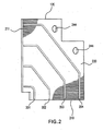
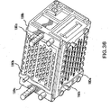
図1は、本発明の好適な実施形態の例によるコネクタ100の分解図である。理解を容易にするために、いくつかの構成要素は省かれている。図1に示すように、コネクタ100は、導電体を上部にプリントした少なくとも1つのプリント回路基板120を含み得る。図示した実施形態では、コネクタ100はさらに、スペーサー対110aおよび110b、インターポーザー対180aおよび180b、エンドキャップ対199(199aおよび199b)、バックボーン150、シールド160およびエンドプレート対190(すなわち190aおよび190b)を含み得る。図1には1つの回路基板および2つのスペーサーしか示していないが、当業者であれば、後に述べるように、典型的な構成ではコネクタ100は多数の回路基板およびスペーサーを含み、各回路基板が2つのスペーサーの間に配置されることは理解されよう。
6、要素1520を参照)。
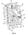
を含む。フィンガー435および437は各々突起部436および438を含む。突起部は、対応するインターポーザー内の対応する窪みにはめ込むのが可能なほどに十分に弾性がある。
は、Bタイプ基板はAタイプ基板より導電体が1つ少ない。
らなっていてもよいことは理解されよう。
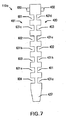
ことを示すために、同図にはスペーサー110は示されていない。図21はまた2つのセル1570を示しており、各々がインターポーザー180の開口部に配置されている。図21に示すように、各セル1570のコンタクト部材1530は対応する導体と物理的に接触する。
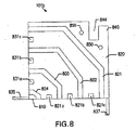
加えるため、スプリング1520によって、ハウジング1522が基板2190から離れる方向に移動する大きさが制限される。これは、スプリングの遠位端はスペーサー110の表面に当接し、またスペーサーはインターポーザー180にしっかりと取り付けられており、インターポーザー自体は基板2190に対して移動しないために生じる。よって、スプリング1520は収縮し、ハウジングに正常な力とは反対方向の力を加える。
図37〜図46は本発明のいくつかの他の好適な実施形態を示す。特に、図37〜図46に示す実施態様は上述した実施形態に大体において類似しており、商業上の応用例も類似している。しかし、図37〜図46に示す実施形態は好ましくは、コンプライアントピン接続部を持つ2ピースコネクタを含む。
導電体をその面に(例えば、プリントまたは他の方法で形成して)有する少なくとも1つのプリント回路基板120−Cと、複数のスペーサー110−C(例えば、図示したスペーサー110a−Cおよび110b−C)とを含む。さらに、いくつかの例示的な実施形態では、改変コネクタはまた、図37〜図46を参照して述べる構成要素を維持するための支持構造物、包囲構造物および/またはその他の構造物を含む。例えば、いくつかの例示的であって非限定的実施形態では、以下のもの、すなわちエンドキャップ対(例えば上述のものを参照、図37〜図46には示さず)、バックボーン(例えば上述のものを参照、図37〜図46には示さず)、シールド(例えば上述のものを参照、図37〜図46には示さず)およびエンドプレート対(例えば上述のものを参照、図37〜図46には示さず)のうちの1つ以上、好ましくはすべてを含む。上述の実施形態におけるように、典型的な構成では、改変コネクタ110は多数の回路基板およびスペーサーを含むことは当業者であれば理解されよう。
。
(注:インターポーザーの各々は総称して参照番号180−Cとしても示される)。フィンガーは例えば図37、図38および図40に最もよく示される。図示するように、好適な実施形態では、スペーサー110−Cのうちの複数のもの、またはこれらのすべてが各々、少なくとも1つ、好ましくは2つの、第1インターポーザー180−C1と係合する突出フィンガーを、および/または少なくとも1つ、好ましくは2つの、第2インターポーザー180−C2と係合する突出フィンガーを含む。これらフィンガーは各々のインターポーザー内の各々の受容スロット内で係合する。中でも、このようなフィンガーおよびスロットの係合は、第1インターポーザーと(例えば、ドーターカードに取り付けられた)コネクタ本体とを組み立てるとき、および/または2ピースコネクタの2つの部分を互いに接続させるとき(例えば、ドーターカードをカードケージに滑り込ますとき)に、例えばプリント回路基板のアラインメントを容易にするなど、有利となり得る。
部材の近位端1641a−Cおよび1641b−Cがハウジング1522−Cの底面を越えて突き出ることができるように、ハウジングの上面から底面へと延びている。図45に示すように、いくつかの好適な実施形態では、ほぼ方形の開口部が、ハウジング1522−Cを貫通するほぼI形状の通路1522I内に設けられている。特に、ほぼI形状の通路1522Iを使用することで、例えばハウジング1522−Cの膨張能力を高めることによって、コンタクト部材のハウジング内への挿入を容易にすることができる。用語V形状と同様に、用語I形状は一般的に解釈され、正確にI形状である必要はなく、広い部分(例えば1522rなど)が別の部分を介して接続または実質的に接続されるような構成を包含する。
落ちるのを防ぐのを助けるタブを含むことができる。
み立てられると、インターポーザー180−Cは各基板(例えば、マザーボードおよびドーターボードなど)に面しこれとほぼ平行となる。例として、図42は、基板2190−Cに面しこれとほぼ平行であるインターポーザー180−Cを示す。
、d)スペーサー溝互い違い間隔距離(図42において参照番号0.094で示す)約0.094インチ、e)ハウジング1522−Cの深さ距離(図43において参照番号0.24で示す)約0.24インチ、f)ハウジング1522−Cの幅距離(図43において参照番号0.13で示す)約0.13インチ、g)コンタクトピン延長距離(図43において参照番号0.04で示す)約0.04インチ、およびh)コンタクトピン間隔距離(図43において参照番号0.06で示す)約0.06インチ、のうちの少なくともいくつかまたは好ましくはすべてを有する構成要素含むことができる。
送ラインを用いる。
Claims (22)
- 相互接続システムであって、
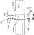
第1回路基板(2190、図21;2190−C、図44)であって、(a)第1差動相互接続経路(2196a、2196b、図22)と、(b)前記第1回路基板の表面の第1ソケット(2194−C、図44)と、(c)同じく前記第1回路基板の前記表面の第2ソケット(2194−C、図44)とを備えた第1回路基板であって、前記第1差動相互接続経路(2196a、2196b、図22)は、前記第1ソケットに電気的に接続された第1信号経路(2196a、図22)と前記第2ソケットに電気的に接続された第2信号経路(2196b、図22)とを備えている、第1回路基板と、
第2差動相互接続経路を備えた第2回路基板(2180、図21)と、
前記第1差動相互接続経路を前記第2差動相互接続経路と電気的に接続させるコネクタ(図37)であって、
第1面と前記第1面とは反対側の第2面とを有するインターポーザー(180−C1、図37)であって、前記第1面は前記第1回路基板の前記表面に面しており、前記インターポーザーの前記第1面から前記インターポーザーの前記第2面まで延びる開口部(1811−C、図38)の配列を含む、インターポーザーと、
前記インターポーザーの前記第2面に隣接する端部を有する第1導体(201、図2;201−C、図39)と、
前記第1導体とほぼ平行であり長さがほぼ等しい第2導体(301、図3)であって、同じく前記インターポーザーの前記第2面に隣接する端部を有する第2導体と、
前記第1導体と前記第2導体との間に配置される誘電材料(120、図1;120−C、図39)と、
前記開口部の配列内に位置する複数のセル(122−C、図37)であって、各々が第1の細長いコンタクト部材(1530a−C、図43)と第2の細長いコンタクト部材(1530b−C、図43)とを支持するハウジング(1522−C、図45)を含むセルとを備え、
前記第1の細長いコンタクト部材(1530a−C)は導体接触部(1745−C、図43)と基板接触部(1641−C、図41)と前記導体接触部と前記基板接触部との間の中間部とを有し、前記導体接触部は前記第1導体(201、201−C)の前記端部と物理的に接触し、前記基板接触部(1641−C)は前記第1ソケット(2194−C)と物理的に接触し且つ従順に係合し、そして前記中間部の少なくとも一部は前記ハウジングのうちの第1ハウジングと係合し、
前記第2の細長いコンタクト部材(1530b−C)は導体接触部と基板接触部と前記導体接触部と前記基板接触部との間の中間部とを有し、前記導体接触部は前記第2導体の前記第1端部と物理的に接触し、前記基板接触部は前記第2ソケットと物理的に接触し且つ従順に係合し、そして前記中間部の少なくとも一部は前記ハウジングのうちの前記第1ハウジングと係合している、
相互接続システム。 - 前記ハウジングは誘電性材料により製造される、請求項1に記載の相互接続システム。
- 前記ハウジングは誘電性材料により製造され、前記インターポーザーは導電性材料により製造されるかまたは導電性材料により被覆される、請求項1に記載の相互接続システム。
- 前記インターポーザーは金属により製造される、請求項3に記載の相互接続システム。
- 前記第1導体と前記第2導体との間に配置される前記誘電性材料は、第1面と第2面とを有する第3の回路基板を構成する、請求項1に記載の相互接続システム。
- 前記第1導体は前記第3の回路基板の前記第1面に配置され、前記第2導体は前記第3の回路基板の前記第2面に配置される、請求項5に記載の相互接続システム。
- 前記第3の回路基板は第1スペーサーと第2スペーサーとの間に挟まれる、請求項6に記載の相互接続システム。
- 前記第1スペーサーはその第1面に溝を持ち、前記溝は前記第1導体と位置が合いまたこれを反映する、請求項7に記載の相互接続システム。
- 前記第1スペーサーは前記スペーサーを前記インターポーザーに取り付けるための少なくとも1つのフィンガーを有する、請求項7に記載の相互接続システム。
- 前記インターポーザーは前記少なくとも1つのフィンガーを受容するための少なくとも1つの窪みを有する、請求項9に記載の相互接続システム。
- 前記第2スペーサーはその第1面に溝を持ち、前記溝は前記第2導体と位置が合いまたこれを反映する、請求項8に記載の相互接続システム。
- 前記ハウジングのうちの前記第1ハウジングは、前記第3の回路基板を受容するようにされたスロットを含む、請求項1に記載の相互接続システム。
- 前記ハウジングのうちの前記第1ハウジングはさらに、前記第1および第2の細長いコンタクト部材の前記導体接触部を受容するようにされたチャネルを含む、請求項12に記載の相互接続システム。
- 前記導体接触部は前記チャネル内に柔軟に収容され、また前記チャネルは前記第1および第2の細長いコンタクト部材の各々の遠位端を越えて延びる、請求項13に記載の相互接続システム。
- 前記基板接触部は約0.04インチより小さい直径のピンを含む、請求項1に記載の相互接続システム。
- 前記基板接触部は約0.03インチより小さい直径のピンを含む、請求項1に記載の相互接続システム。
- 前記基板接触部は約0.02インチより小さい直径のピンを含む、請求項1に記載の相互接続システム。
- 前記ハウジングは約0.3インチより小さい幅を有する、請求項1に記載の相互接続システム。
- 前記ハウジングは約0.2インチより小さい幅を有する、請求項1に記載の相互接続システム。
- 前記ハウジングは約0.15インチより小さい幅を有する、請求項1に記載の相互接続システム。
- 前記コネクタは約5GBPSより高い差動応用例をサポートする、請求項1に記載の相互接続システム。
- 前記コネクタは約10GBPSより高い差動応用例をサポートする、請求項1に記載の相互接続システム。
Applications Claiming Priority (2)
| Application Number | Priority Date | Filing Date | Title |
|---|---|---|---|
| US48758003P | 2003-07-17 | 2003-07-17 | |
| PCT/US2004/023096 WO2005011061A2 (en) | 2003-07-17 | 2004-07-19 | High-speed electrical connector |
Related Child Applications (1)
| Application Number | Title | Priority Date | Filing Date |
|---|---|---|---|
| JP2010153286A Division JP5027907B2 (ja) | 2003-07-17 | 2010-07-05 | 高速電気コネクタ |
Publications (2)
| Publication Number | Publication Date |
|---|---|
| JP2007531964A JP2007531964A (ja) | 2007-11-08 |
| JP4590406B2 true JP4590406B2 (ja) | 2010-12-01 |
Family
ID=34102700
Family Applications (3)
| Application Number | Title | Priority Date | Filing Date |
|---|---|---|---|
| JP2006520397A Expired - Fee Related JP4570619B2 (ja) | 2003-07-17 | 2004-07-19 | 高速電気コネクタ |
| JP2006520396A Expired - Fee Related JP4590406B2 (ja) | 2003-07-17 | 2004-07-19 | 高速電気コネクタ |
| JP2010153286A Expired - Fee Related JP5027907B2 (ja) | 2003-07-17 | 2010-07-05 | 高速電気コネクタ |
Family Applications Before (1)
| Application Number | Title | Priority Date | Filing Date |
|---|---|---|---|
| JP2006520397A Expired - Fee Related JP4570619B2 (ja) | 2003-07-17 | 2004-07-19 | 高速電気コネクタ |
Family Applications After (1)
| Application Number | Title | Priority Date | Filing Date |
|---|---|---|---|
| JP2010153286A Expired - Fee Related JP5027907B2 (ja) | 2003-07-17 | 2010-07-05 | 高速電気コネクタ |
Country Status (5)
| Country | Link |
|---|---|
| EP (2) | EP1652273A4 (ja) |
| JP (3) | JP4570619B2 (ja) |
| AU (2) | AU2004260456C1 (ja) |
| CA (2) | CA2532141C (ja) |
| WO (2) | WO2005011061A2 (ja) |
Families Citing this family (19)
| Publication number | Priority date | Publication date | Assignee | Title |
|---|---|---|---|---|
| US7074047B2 (en) * | 2003-11-05 | 2006-07-11 | Tensolite Company | Zero insertion force high frequency connector |
| US20090291593A1 (en) | 2005-06-30 | 2009-11-26 | Prescott Atkinson | High frequency broadside-coupled electrical connector |
| US7914304B2 (en) | 2005-06-30 | 2011-03-29 | Amphenol Corporation | Electrical connector with conductors having diverging portions |
| JP4521834B2 (ja) * | 2008-01-17 | 2010-08-11 | 日本航空電子工業株式会社 | コネクタ |
| JP5284759B2 (ja) * | 2008-11-17 | 2013-09-11 | 京セラコネクタプロダクツ株式会社 | コネクタ及びコネクタの製造方法 |
| WO2011140438A2 (en) | 2010-05-07 | 2011-11-10 | Amphenol Corporation | High performance cable connector |
| WO2012106554A2 (en) | 2011-02-02 | 2012-08-09 | Amphenol Corporation | Mezzanine connector |
| CN102522645B (zh) * | 2011-12-15 | 2013-10-09 | 深圳格力浦电子有限公司 | 一种背板连接器的近端串扰改善方法 |
| WO2014031851A1 (en) | 2012-08-22 | 2014-02-27 | Amphenol Corporation | High-frequency electrical connector |
| CN106104933B (zh) | 2014-01-22 | 2020-09-11 | 安费诺有限公司 | 具有被屏蔽的信号路径的高速高密度电连接器 |
| CN108701922B (zh) | 2015-07-07 | 2020-02-14 | Afci亚洲私人有限公司 | 电连接器 |
| CN109863650B (zh) | 2016-08-23 | 2020-10-02 | 安费诺有限公司 | 可配置为高性能的连接器 |
| US9997868B1 (en) * | 2017-07-24 | 2018-06-12 | Te Connectivity Corporation | Electrical connector with improved impedance characteristics |
| CN110707493B (zh) * | 2018-07-10 | 2021-08-31 | 莫列斯有限公司 | 中介转接连接器及电连接器组合 |
| CN208862209U (zh) | 2018-09-26 | 2019-05-14 | 安费诺东亚电子科技(深圳)有限公司 | 一种连接器及其应用的pcb板 |
| TW202135385A (zh) | 2020-01-27 | 2021-09-16 | 美商Fci美國有限責任公司 | 高速連接器 |
| US11469554B2 (en) | 2020-01-27 | 2022-10-11 | Fci Usa Llc | High speed, high density direct mate orthogonal connector |
| CN215816516U (zh) | 2020-09-22 | 2022-02-11 | 安费诺商用电子产品(成都)有限公司 | 电连接器 |
| CN213636403U (zh) | 2020-09-25 | 2021-07-06 | 安费诺商用电子产品(成都)有限公司 | 电连接器 |
Family Cites Families (10)
| Publication number | Priority date | Publication date | Assignee | Title |
|---|---|---|---|---|
| US5007843A (en) * | 1983-05-31 | 1991-04-16 | Trw Inc. | High-density contact area electrical connectors |
| US6540558B1 (en) * | 1995-07-03 | 2003-04-01 | Berg Technology, Inc. | Connector, preferably a right angle connector, with integrated PCB assembly |
| US5993259A (en) * | 1997-02-07 | 1999-11-30 | Teradyne, Inc. | High speed, high density electrical connector |
| US6179663B1 (en) * | 1998-04-29 | 2001-01-30 | Litton Systems, Inc. | High density electrical interconnect system having enhanced grounding and cross-talk reduction capability |
| KR100639560B1 (ko) * | 1999-11-24 | 2006-10-30 | 테라다인 인코퍼레이티드 | 차동 신호 전기 커넥터용 인쇄회로기판 |
| EP1256147A2 (en) * | 2000-02-03 | 2002-11-13 | Teradyne, Inc. | High speed pressure mount connector |
| US6267604B1 (en) * | 2000-02-03 | 2001-07-31 | Tyco Electronics Corporation | Electrical connector including a housing that holds parallel circuit boards |
| US6843657B2 (en) * | 2001-01-12 | 2005-01-18 | Litton Systems Inc. | High speed, high density interconnect system for differential and single-ended transmission applications |
| US6712648B2 (en) * | 2002-07-24 | 2004-03-30 | Litton Systems, Inc. | Laminate electrical interconnect system |
| AU2003263799A1 (en) * | 2002-07-24 | 2004-02-09 | Litton Systems, Inc. | Interconnection system |
-
2004
- 2004-07-19 EP EP04757111A patent/EP1652273A4/en not_active Withdrawn
- 2004-07-19 EP EP04757110A patent/EP1652276A4/en not_active Withdrawn
- 2004-07-19 WO PCT/US2004/023096 patent/WO2005011061A2/en active Application Filing
- 2004-07-19 JP JP2006520397A patent/JP4570619B2/ja not_active Expired - Fee Related
- 2004-07-19 CA CA2532141A patent/CA2532141C/en not_active Expired - Fee Related
- 2004-07-19 WO PCT/US2004/023098 patent/WO2005011062A2/en active Search and Examination
- 2004-07-19 AU AU2004260456A patent/AU2004260456C1/en not_active Ceased
- 2004-07-19 JP JP2006520396A patent/JP4590406B2/ja not_active Expired - Fee Related
- 2004-07-19 AU AU2004260455A patent/AU2004260455B8/en not_active Ceased
- 2004-07-19 CA CA2532378A patent/CA2532378C/en not_active Expired - Fee Related
-
2010
- 2010-07-05 JP JP2010153286A patent/JP5027907B2/ja not_active Expired - Fee Related
Also Published As
| Publication number | Publication date |
|---|---|
| JP2007524196A (ja) | 2007-08-23 |
| JP5027907B2 (ja) | 2012-09-19 |
| CA2532378C (en) | 2011-12-20 |
| CA2532378A1 (en) | 2005-02-03 |
| WO2005011062A3 (en) | 2005-08-11 |
| AU2004260456C1 (en) | 2010-06-24 |
| AU2004260455B2 (en) | 2009-06-18 |
| EP1652276A2 (en) | 2006-05-03 |
| EP1652276A4 (en) | 2008-01-02 |
| CA2532141A1 (en) | 2005-02-03 |
| AU2004260455B8 (en) | 2009-09-17 |
| WO2005011062A2 (en) | 2005-02-03 |
| WO2005011061A3 (en) | 2005-04-28 |
| WO2005011061A2 (en) | 2005-02-03 |
| AU2004260455A1 (en) | 2005-02-03 |
| EP1652273A4 (en) | 2008-01-02 |
| JP2010251335A (ja) | 2010-11-04 |
| AU2004260456A1 (en) | 2005-02-03 |
| JP2007531964A (ja) | 2007-11-08 |
| AU2004260456B2 (en) | 2009-12-10 |
| JP4570619B2 (ja) | 2010-10-27 |
| EP1652273A2 (en) | 2006-05-03 |
| CA2532141C (en) | 2012-04-17 |
Similar Documents
| Publication | Publication Date | Title |
|---|---|---|
| JP5027907B2 (ja) | 高速電気コネクタ | |
| US7040901B2 (en) | High-speed electrical connector | |
| US6979202B2 (en) | High-speed electrical connector | |
| US9455530B2 (en) | Electrical connector with ground bus | |
| TWI764267B (zh) | 電子連接器 | |
| US20170264053A1 (en) | Connector and connector system | |
| US5378160A (en) | Compliant stacking connector for printed circuit boards | |
| US7837492B2 (en) | Electrical connector having matched impedance by contacts having node arrangement | |
| US6923659B2 (en) | Electrical connector with improved terminals | |
| TWI593172B (zh) | Connector | |
| US7438556B2 (en) | Electrical interconnection between multiple printed circuit boards | |
| JP2014531723A (ja) | 電気接点及びコネクタ | |
| US7604508B1 (en) | Electrical connector utilizing contact array | |
| US9257768B2 (en) | Electrical connector with robust heat-dissipation structures | |
| US6840809B2 (en) | Electrical connector having improved contacts | |
| US6227874B1 (en) | Electronic card connection system | |
| CN114208404A (zh) | 卡边缘连接器系统 | |
| TWM625197U (zh) | 電連接器 | |
| CN115776011A (zh) | 电连接器 |
Legal Events
| Date | Code | Title | Description |
|---|---|---|---|
| A131 | Notification of reasons for refusal |
Free format text: JAPANESE INTERMEDIATE CODE: A131 Effective date: 20091124 |
|
| A521 | Written amendment |
Free format text: JAPANESE INTERMEDIATE CODE: A523 Effective date: 20100212 |
|
| A131 | Notification of reasons for refusal |
Free format text: JAPANESE INTERMEDIATE CODE: A131 Effective date: 20100406 |
|
| A521 | Written amendment |
Free format text: JAPANESE INTERMEDIATE CODE: A523 Effective date: 20100705 |
|
| TRDD | Decision of grant or rejection written | ||
| A01 | Written decision to grant a patent or to grant a registration (utility model) |
Free format text: JAPANESE INTERMEDIATE CODE: A01 Effective date: 20100817 |
|
| A01 | Written decision to grant a patent or to grant a registration (utility model) |
Free format text: JAPANESE INTERMEDIATE CODE: A01 |
|
| A61 | First payment of annual fees (during grant procedure) |
Free format text: JAPANESE INTERMEDIATE CODE: A61 Effective date: 20100913 |
|
| R150 | Certificate of patent or registration of utility model |
Free format text: JAPANESE INTERMEDIATE CODE: R150 |
|
| FPAY | Renewal fee payment (event date is renewal date of database) |
Free format text: PAYMENT UNTIL: 20130917 Year of fee payment: 3 |
|
| R250 | Receipt of annual fees |
Free format text: JAPANESE INTERMEDIATE CODE: R250 |
|
| LAPS | Cancellation because of no payment of annual fees |