JP4584261B2 - Manufacturing of cooling and heat exchange system by electroforming - Google Patents
Manufacturing of cooling and heat exchange system by electroforming Download PDFInfo
- Publication number
- JP4584261B2 JP4584261B2 JP2006540364A JP2006540364A JP4584261B2 JP 4584261 B2 JP4584261 B2 JP 4584261B2 JP 2006540364 A JP2006540364 A JP 2006540364A JP 2006540364 A JP2006540364 A JP 2006540364A JP 4584261 B2 JP4584261 B2 JP 4584261B2
- Authority
- JP
- Japan
- Prior art keywords
- mask layer
- metal
- metal layer
- layer
- thickness
- Prior art date
- Legal status (The legal status is an assumption and is not a legal conclusion. Google has not performed a legal analysis and makes no representation as to the accuracy of the status listed.)
- Expired - Fee Related
Links
Images


Classifications
-
- C—CHEMISTRY; METALLURGY
- C25—ELECTROLYTIC OR ELECTROPHORETIC PROCESSES; APPARATUS THEREFOR
- C25D—PROCESSES FOR THE ELECTROLYTIC OR ELECTROPHORETIC PRODUCTION OF COATINGS; ELECTROFORMING; APPARATUS THEREFOR
- C25D1/00—Electroforming
- C25D1/08—Perforated or foraminous objects, e.g. sieves
-
- C—CHEMISTRY; METALLURGY
- C25—ELECTROLYTIC OR ELECTROPHORETIC PROCESSES; APPARATUS THEREFOR
- C25D—PROCESSES FOR THE ELECTROLYTIC OR ELECTROPHORETIC PRODUCTION OF COATINGS; ELECTROFORMING; APPARATUS THEREFOR
- C25D1/00—Electroforming
- C25D1/003—3D structures, e.g. superposed patterned layers
-
- C—CHEMISTRY; METALLURGY
- C25—ELECTROLYTIC OR ELECTROPHORETIC PROCESSES; APPARATUS THEREFOR
- C25D—PROCESSES FOR THE ELECTROLYTIC OR ELECTROPHORETIC PRODUCTION OF COATINGS; ELECTROFORMING; APPARATUS THEREFOR
- C25D1/00—Electroforming
- C25D1/02—Tubes; Rings; Hollow bodies
-
- F—MECHANICAL ENGINEERING; LIGHTING; HEATING; WEAPONS; BLASTING
- F23—COMBUSTION APPARATUS; COMBUSTION PROCESSES
- F23M—CASINGS, LININGS, WALLS OR DOORS SPECIALLY ADAPTED FOR COMBUSTION CHAMBERS, e.g. FIREBRIDGES; DEVICES FOR DEFLECTING AIR, FLAMES OR COMBUSTION PRODUCTS IN COMBUSTION CHAMBERS; SAFETY ARRANGEMENTS SPECIALLY ADAPTED FOR COMBUSTION APPARATUS; DETAILS OF COMBUSTION CHAMBERS, NOT OTHERWISE PROVIDED FOR
- F23M5/00—Casings; Linings; Walls
- F23M5/08—Cooling thereof; Tube walls
-
- F—MECHANICAL ENGINEERING; LIGHTING; HEATING; WEAPONS; BLASTING
- F23—COMBUSTION APPARATUS; COMBUSTION PROCESSES
- F23R—GENERATING COMBUSTION PRODUCTS OF HIGH PRESSURE OR HIGH VELOCITY, e.g. GAS-TURBINE COMBUSTION CHAMBERS
- F23R3/00—Continuous combustion chambers using liquid or gaseous fuel
- F23R3/005—Combined with pressure or heat exchangers
-
- F—MECHANICAL ENGINEERING; LIGHTING; HEATING; WEAPONS; BLASTING
- F28—HEAT EXCHANGE IN GENERAL
- F28F—DETAILS OF HEAT-EXCHANGE AND HEAT-TRANSFER APPARATUS, OF GENERAL APPLICATION
- F28F13/00—Arrangements for modifying heat-transfer, e.g. increasing, decreasing
- F28F13/06—Arrangements for modifying heat-transfer, e.g. increasing, decreasing by affecting the pattern of flow of the heat-exchange media
- F28F13/08—Arrangements for modifying heat-transfer, e.g. increasing, decreasing by affecting the pattern of flow of the heat-exchange media by varying the cross-section of the flow channels
-
- F—MECHANICAL ENGINEERING; LIGHTING; HEATING; WEAPONS; BLASTING
- F28—HEAT EXCHANGE IN GENERAL
- F28F—DETAILS OF HEAT-EXCHANGE AND HEAT-TRANSFER APPARATUS, OF GENERAL APPLICATION
- F28F3/00—Plate-like or laminated elements; Assemblies of plate-like or laminated elements
- F28F3/12—Elements constructed in the shape of a hollow panel, e.g. with channels
-
- F—MECHANICAL ENGINEERING; LIGHTING; HEATING; WEAPONS; BLASTING
- F28—HEAT EXCHANGE IN GENERAL
- F28F—DETAILS OF HEAT-EXCHANGE AND HEAT-TRANSFER APPARATUS, OF GENERAL APPLICATION
- F28F7/00—Elements not covered by group F28F1/00, F28F3/00 or F28F5/00
- F28F7/02—Blocks traversed by passages for heat-exchange media
-
- G—PHYSICS
- G02—OPTICS
- G02B—OPTICAL ELEMENTS, SYSTEMS OR APPARATUS
- G02B7/00—Mountings, adjusting means, or light-tight connections, for optical elements
- G02B7/18—Mountings, adjusting means, or light-tight connections, for optical elements for prisms; for mirrors
- G02B7/181—Mountings, adjusting means, or light-tight connections, for optical elements for prisms; for mirrors with means for compensating for changes in temperature or for controlling the temperature; thermal stabilisation
- G02B7/1815—Mountings, adjusting means, or light-tight connections, for optical elements for prisms; for mirrors with means for compensating for changes in temperature or for controlling the temperature; thermal stabilisation with cooling or heating systems
-
- F—MECHANICAL ENGINEERING; LIGHTING; HEATING; WEAPONS; BLASTING
- F23—COMBUSTION APPARATUS; COMBUSTION PROCESSES
- F23M—CASINGS, LININGS, WALLS OR DOORS SPECIALLY ADAPTED FOR COMBUSTION CHAMBERS, e.g. FIREBRIDGES; DEVICES FOR DEFLECTING AIR, FLAMES OR COMBUSTION PRODUCTS IN COMBUSTION CHAMBERS; SAFETY ARRANGEMENTS SPECIALLY ADAPTED FOR COMBUSTION APPARATUS; DETAILS OF COMBUSTION CHAMBERS, NOT OTHERWISE PROVIDED FOR
- F23M2900/00—Special features of, or arrangements for combustion chambers
- F23M2900/05003—Details of manufacturing specially adapted for combustion chambers
-
- F—MECHANICAL ENGINEERING; LIGHTING; HEATING; WEAPONS; BLASTING
- F23—COMBUSTION APPARATUS; COMBUSTION PROCESSES
- F23M—CASINGS, LININGS, WALLS OR DOORS SPECIALLY ADAPTED FOR COMBUSTION CHAMBERS, e.g. FIREBRIDGES; DEVICES FOR DEFLECTING AIR, FLAMES OR COMBUSTION PRODUCTS IN COMBUSTION CHAMBERS; SAFETY ARRANGEMENTS SPECIALLY ADAPTED FOR COMBUSTION APPARATUS; DETAILS OF COMBUSTION CHAMBERS, NOT OTHERWISE PROVIDED FOR
- F23M2900/00—Special features of, or arrangements for combustion chambers
- F23M2900/05004—Special materials for walls or lining
-
- F—MECHANICAL ENGINEERING; LIGHTING; HEATING; WEAPONS; BLASTING
- F28—HEAT EXCHANGE IN GENERAL
- F28F—DETAILS OF HEAT-EXCHANGE AND HEAT-TRANSFER APPARATUS, OF GENERAL APPLICATION
- F28F2260/00—Heat exchangers or heat exchange elements having special size, e.g. microstructures
-
- Y—GENERAL TAGGING OF NEW TECHNOLOGICAL DEVELOPMENTS; GENERAL TAGGING OF CROSS-SECTIONAL TECHNOLOGIES SPANNING OVER SEVERAL SECTIONS OF THE IPC; TECHNICAL SUBJECTS COVERED BY FORMER USPC CROSS-REFERENCE ART COLLECTIONS [XRACs] AND DIGESTS
- Y02—TECHNOLOGIES OR APPLICATIONS FOR MITIGATION OR ADAPTATION AGAINST CLIMATE CHANGE
- Y02T—CLIMATE CHANGE MITIGATION TECHNOLOGIES RELATED TO TRANSPORTATION
- Y02T50/00—Aeronautics or air transport
- Y02T50/60—Efficient propulsion technologies, e.g. for aircraft
-
- Y—GENERAL TAGGING OF NEW TECHNOLOGICAL DEVELOPMENTS; GENERAL TAGGING OF CROSS-SECTIONAL TECHNOLOGIES SPANNING OVER SEVERAL SECTIONS OF THE IPC; TECHNICAL SUBJECTS COVERED BY FORMER USPC CROSS-REFERENCE ART COLLECTIONS [XRACs] AND DIGESTS
- Y10—TECHNICAL SUBJECTS COVERED BY FORMER USPC
- Y10T—TECHNICAL SUBJECTS COVERED BY FORMER US CLASSIFICATION
- Y10T29/00—Metal working
- Y10T29/49—Method of mechanical manufacture
- Y10T29/49002—Electrical device making
- Y10T29/49117—Conductor or circuit manufacturing
-
- Y—GENERAL TAGGING OF NEW TECHNOLOGICAL DEVELOPMENTS; GENERAL TAGGING OF CROSS-SECTIONAL TECHNOLOGIES SPANNING OVER SEVERAL SECTIONS OF THE IPC; TECHNICAL SUBJECTS COVERED BY FORMER USPC CROSS-REFERENCE ART COLLECTIONS [XRACs] AND DIGESTS
- Y10—TECHNICAL SUBJECTS COVERED BY FORMER USPC
- Y10T—TECHNICAL SUBJECTS COVERED BY FORMER US CLASSIFICATION
- Y10T29/00—Metal working
- Y10T29/49—Method of mechanical manufacture
- Y10T29/494—Fluidic or fluid actuated device making
-
- Y—GENERAL TAGGING OF NEW TECHNOLOGICAL DEVELOPMENTS; GENERAL TAGGING OF CROSS-SECTIONAL TECHNOLOGIES SPANNING OVER SEVERAL SECTIONS OF THE IPC; TECHNICAL SUBJECTS COVERED BY FORMER USPC CROSS-REFERENCE ART COLLECTIONS [XRACs] AND DIGESTS
- Y10—TECHNICAL SUBJECTS COVERED BY FORMER USPC
- Y10T—TECHNICAL SUBJECTS COVERED BY FORMER US CLASSIFICATION
- Y10T29/00—Metal working
- Y10T29/49—Method of mechanical manufacture
- Y10T29/4998—Combined manufacture including applying or shaping of fluent material
Description
本発明は種々の形態の業界のための部品に関し、より詳細には、電鋳により冷却および熱交換システムを製造することに関する。 The present invention relates to parts for various forms of industry, and more particularly to manufacturing cooling and heat exchange systems by electroforming.
使用時に高温および/または高圧となっている流体との接触を通して、高温に曝されたり、高温となったりする(一般には金属製の)部品を使用することに関係する多数の技術が存在する。かかる部品として、エネルギーの発生および熱交換システム、ならびに推進システムで使用される部品を挙げることができる。特定の例として、反応容器、燃焼室およびロケットエンジンがある。一般に、かかる部品を冷却したり、ある流体から別の流体に熱交換が行われる部品を提供するニーズがある。 There are a number of techniques involved in using components (typically made of metal) that are exposed to and / or become hot through contact with fluids that are hot and / or high in use. Such components may include components used in energy generation and heat exchange systems, and propulsion systems. Specific examples include reaction vessels, combustion chambers and rocket engines. In general, there is a need to provide such a component that cools such components or that exchanges heat from one fluid to another.
公知のシステムを用いた場合の問題は、冷却または熱交換のレートが所望する値より低いので、かかるシステムの効率が可能な値程度に高くないことである。 The problem with known systems is that the efficiency of such systems is not as high as possible because the rate of cooling or heat exchange is lower than desired.
別の問題は、部品およびシステムを製造するための従来の方法が、統合された冷却/熱交換要素を用いた、および必要な材料における種々の形態の部品の製造に適していないこと、すなわち従来の製造方法の結果、妥協的な設計をするための部品のコストが大幅に増加することである。 Another problem is that conventional methods for manufacturing parts and systems are not suitable for manufacturing various forms of parts using integrated cooling / heat exchange elements and in the required materials, i.e. conventional As a result of this manufacturing method, the cost of parts for making a compromise design is greatly increased.
上記の問題を克服し、製造プロセスおよび部品を改善する製造技術が求められている。更に、かかる部品を低コストで製造するための技術が求められている。 There is a need for manufacturing techniques that overcome the above problems and improve manufacturing processes and components. Furthermore, a technique for manufacturing such a component at a low cost is required.
本発明は、表面を有する物体を設けるステップと、第1の電鋳作業を実行し、前記表面に金属材料を備えた第1金属層を形成するステップと、非導電性材料を含む第1マスク層を前記第1金属層上に形成するステップと、前記第1マスク層にパターン形成し、第1金属層よりも上の前記非導電性材料を除去した、細長い寸法の複数の第1リセスを前記第1マスク層に設けるステップと、前記金属材料を使って第2電鋳作業を実行し、前記第1リセスに前記金属材料を充填し、前記第1マスク層よりも上にあって、前記第1マスク層の表面全体またはその一部を覆い、少なくとも第1の所定の厚みに延び、前記金属材料を含む第2金属層を形成するステップとを備えた、金属部品を製造するための方法を提供するものである。 The present invention includes providing an object having a surface, performing a first electroforming operation to form a first metal layer having a metal material on the surface, and a first mask including a non-conductive material Forming a layer on the first metal layer; patterning the first mask layer; removing a plurality of elongate first recesses with the non-conductive material above the first metal layer removed. Providing the first mask layer, performing a second electroforming operation using the metal material, filling the first recess with the metal material, and being above the first mask layer, Forming a second metal layer that covers the entire surface of the first mask layer or a part thereof, extends to at least a first predetermined thickness and includes the metal material, and a method for manufacturing a metal part Is to provide.
前記物体は、基板を備え、前記表面は、前記基板の平坦な、または実質的に平坦な表面を備える。または前記物体は、異形マンドレル(このマンドレルは、例えば機械加工により正当な範囲内で任意の形状でよい)含み、このマンドレルは、前記表面を(例えばネガとして)構成し、該表面は、例えば円筒形、円錐形、放物形、双曲線形、楕円形または球形である。 The object comprises a substrate, and the surface comprises a flat or substantially flat surface of the substrate. Or the object comprises a deformed mandrel (this mandrel may be of any shape within a reasonable range, for example by machining), the mandrel constituting the surface (for example as a negative), the surface being for example a cylinder Shape, cone, parabola, hyperbola, ellipse or sphere.
本方法は、前記第2金属層を機械加工し、均一な厚みの第2金属層を形成するステップを備え、よって前記第2金属層は上部表面を有する。本方法は、物体を除去すると共に前記第2マスク層の前記非導電性材料を除去し、よって前記非導電性材料が除かれた内部に細長い第1チャンネルが延びる金属部品を製造するステップを更に備える。 The method includes machining the second metal layer to form a second metal layer having a uniform thickness, so that the second metal layer has an upper surface. The method further includes removing the object and removing the non-conductive material of the second mask layer, thereby producing a metal component having an elongated first channel extending therein from which the non-conductive material has been removed. Prepare.
本発明の別に様相によれば、本方法は、非導電性材料を含む第2マスク層を前記第2金属層上に形成するステップと、前記第2マスク層にパターン形成し、第2金属層よりも上の前記非導電性材料を除去した、細長い寸法の複数の第2リセスを前記第2マスク層に設けるステップと、前記金属材料を使って第3電鋳作業を実行し、前記第2リセスに前記金属材料を充填し、少なくとも第2の所定の厚みに延び、前記第2マスク層の表面全体またはその一部を覆う、前記金属材料を含む第3金属層を形成するステップとを備える。 According to another aspect of the present invention, the method includes forming a second mask layer including a non-conductive material on the second metal layer, patterning the second mask layer, and forming a second metal layer. Providing the second mask layer with a plurality of elongated recesses having the non-conductive material removed thereon, and performing a third electroforming operation using the metal material; Filling the recess with the metal material, and forming a third metal layer containing the metal material extending to at least a second predetermined thickness and covering the entire surface of the second mask layer or a part thereof. .
本方法は、前記第3金属層を機械加工し、均一な厚みの第3金属層を形成するステップを備えることが好ましく、この第3金属層は、上部層を有する。本方法は、物体を除去すると共に前記第1マスク層および前記第2マスク層の非導電性材料を除去し、よって前記第1マスク層の非導電性材料が除かれた内部に延びる細長い第1チャンネルを有すると共に、前記第2マスク層の非導電性材料が除去された、内部に延びる細長い第2チャンネルを有する金属製部品を製造するステップを更に備えることが好ましい。 Preferably, the method comprises the step of machining the third metal layer to form a third metal layer of uniform thickness, the third metal layer having an upper layer. The method removes an object and removes the non-conductive material of the first mask layer and the second mask layer, and thus the elongated first extending into the interior of the first mask layer where the non-conductive material is removed. Preferably, the method further comprises the step of manufacturing a metal part having a channel and an elongated second channel extending inward, wherein the non-conductive material of the second mask layer is removed.
種々のパターン構造が可能であり、従って
(a)前記第1リセスのほうが前記第2リセスよりも幅が広いか、またはこの逆であり、および/または
(b)前記細長い第1チャンネルのほうが前記細長い第2チャンネルよりも幅が広いか、またはこの逆となるか、および/または
(c)前記細長い第1チャンネルおよび/または前記細長い第2チャンネルがそれぞれの円周方向に沿って幅または厚みにテーパが付いており、および/または
(d)前記細長い第1チャンネルの円周方向が前記細長い第2チャンネルの円周方向に対して所定の角度、例えば直角となっており、および/または
(e)前記細長い第1チャンネルおよび/または前記細長い第2チャンネルには突起、側壁リセスおよび/またはバッフルが設けられ、よってかかるチャンネルを通過する直線状でない流れが得られるように、前記第1マスク層にパターン形成するステップおよび/または前記第2マスク層にパターン形成するステップを実行する。
Various pattern structures are possible, so (a) the first recess is wider than the second recess and vice versa, and / or (b) the elongated first channel is more And / or vice versa than the elongated second channel, and / or (c) the elongated first channel and / or the elongated second channel has a width or thickness along their respective circumferential directions. And / or (d) the circumferential direction of the elongated first channel is at a predetermined angle, for example, perpendicular to the circumferential direction of the elongated second channel, and / or (e) ) The elongated first channel and / or the elongated second channel are provided with protrusions, sidewall recesses and / or baffles, and thus So that no straight flow through the tunnel is obtained, performing the step of patterning the steps and / or the second mask layer is patterned on the first mask layer.
一実施例では、第1金属層、第1マスク層および第2金属層が所定の二次元状第1領域を覆って延びるように、第1電鋳作業を実行するステップ、第1マスク層を形成するステップ、前記第1マスク層にパターン形成するステップ、および第2電鋳を実行するステップを実行し、第2金属層、第2マスク層および第3金属層が所定の二次元状第2領域を覆って延びるように第2マスクを形成するステップ、前記第2マスク層にパターン形成するステップ、および第3電鋳作業を実行するステップを実行し、前記二次元状第2領域を前記二次元状第1領域よりも広くする。 In one embodiment, performing the first electroforming operation such that the first metal layer, the first mask layer, and the second metal layer extend over a predetermined two-dimensional first region, Forming a pattern, forming a pattern on the first mask layer, and performing a second electroforming step, wherein the second metal layer, the second mask layer, and the third metal layer have a predetermined two-dimensional second shape. Performing a step of forming a second mask extending over the region, a step of patterning the second mask layer, and a step of performing a third electroforming operation; It is made wider than the dimensional first region.
前記第1金属層の厚みが約100〜200μmとなるように前記第1電鋳作業を実行することが好ましい。前記所定の厚みが少なくとも前記第1金属層の厚みとなるように、前記第2電鋳作業を実行し、前記機械加工ステップが、前記第1金属層の厚みに等しいか、ほぼ等しい厚みまで前記第2金属層を機械加工することが好ましい。 The first electroforming operation is preferably performed so that the thickness of the first metal layer is about 100 to 200 μm. The second electroforming operation is performed such that the predetermined thickness is at least the thickness of the first metal layer, and the machining step is equal to or substantially equal to the thickness of the first metal layer. It is preferred to machine the second metal layer.
上記とは異なり、ある時間にわたって前記第1電鋳作業を実行し、前記第1金属層の厚みが少なくとも前記第1マスク層の厚みと同じ厚みとなり、例えば1〜2mmまたはそれ以上とする。ある時間にわたって前記第2電鋳作業を実行し、前記第2金属層の厚みが少なくとも前記第1マスク層の厚みと同じ厚みとなり、例えば1〜2mmまたはそれ以上とする。 Unlike the above, the first electroforming operation is performed over a period of time, and the thickness of the first metal layer is at least the same as the thickness of the first mask layer, for example, 1 to 2 mm or more. The second electroforming operation is performed over a period of time, and the thickness of the second metal layer is at least the same as the thickness of the first mask layer, for example, 1 to 2 mm or more.
第1マスク層を形成するステップは、前記第1金属層を1〜2mmの厚みまで、前記非導電性材料でコーティングすることが好ましい。前記第2マスク層を形成するステップは、前記第2金属層を1〜2mmの厚みまで、または第1マスク層の厚みよりも厚い厚みまで、非導電性材料でコーティングすることが好ましい。 The step of forming the first mask layer preferably coats the first metal layer with the non-conductive material to a thickness of 1 to 2 mm. In the step of forming the second mask layer, it is preferable to coat the second metal layer with a non-conductive material to a thickness of 1 to 2 mm or thicker than the thickness of the first mask layer.
前記物体および/または前記非導電性材料を除去するステップは、溶剤内に前記非導電性材料を溶解すること、または前記非導電性材料を溶融することが好ましい。 Preferably, the step of removing the object and / or the non-conductive material dissolves the non-conductive material in a solvent or melts the non-conductive material.
一実施例では、前記物体は、例えばスチール、銅または青銅から構成された金属部品である。(例えば、冷却のための)チャンネルの電鋳システムは、物体に取り付けられたままであり、新しい部品を形成する。 In one embodiment, the object is a metal part made of steel, copper or bronze, for example. The channel electroforming system (eg, for cooling) remains attached to the object and forms a new part.
電鋳で使用される前記金属製材料は、ニッケル、銅、キュプロニッケル、セラミック粉末を含有するニッケルまたはセラミック粉末を含有する銅、もしくは鉄および/またはコバルトを含有する合金でよい。最終部品の強度が優先される場合、一般にニッケルが使用され、部品の熱伝達度が良好であることが重要である場合には、銅が使用される。 The metallic material used in electroforming may be nickel, copper, cupronickel, nickel containing ceramic powder or copper containing ceramic powder, or an alloy containing iron and / or cobalt. Nickel is generally used when the strength of the final part is a priority, and copper is used when it is important that the part has good heat transfer.
一実施例では、前記第2電鋳作業で使用される金属材料は、前記第1電鋳作業で使用される金属材料と異なりおよび/または第3電鋳作業で使用される金属材料は前記第2電鋳作業で使用される金属材料と異なる。 In one embodiment, the metal material used in the second electroforming operation is different from the metal material used in the first electroforming operation and / or the metal material used in the third electroforming operation is the first electroforming operation. 2 Different from metal materials used in electroforming operations.
第1マスク層を形成するステップおよび/または第2マスク層を形成するステップで使用される前記非導電性材料は、低融点ポリマー、例えばポリ(メチルメタクリレート)(PMMA)または微小結晶ワックスを含むことが好ましい。 The non-conductive material used in the step of forming the first mask layer and / or the step of forming the second mask layer includes a low melting point polymer, such as poly (methyl methacrylate) (PMMA) or microcrystalline wax. Is preferred.
本発明の別に様相によれば、請求項1〜20のいずれかに記載の方法によって得られる金属部品が提供される。 According to another aspect of the present invention, there is provided a metal part obtained by the method according to any of claims 1-20.
本発明または本発明の実施例の利点として、広範な部品を製造するのに適していることを挙げることができ、一体的な冷却/熱交換システムを提供できるという特別な利点がある。例えば電鋳により、製造プロセス中に一体的に形成された冷却チャンネルを有する金属物体を製造することが可能である。また、外部の寸法または表面仕上げに関して妥協することなく、内部冷却ダクトを有する肉薄の部品(例えばX線または高エネルギーUVミラー、または望遠鏡)を製造したり、構造的な一体性に関して大きな妥協を払うことなく、一体化された細いチューブまたは冷却チャンネルを内部に有する肉厚部分(例えば燃焼室、反応器、ロケットエンジン)を製造することも可能である。 Advantages of the present invention or embodiments of the present invention include the particular advantage that it is suitable for manufacturing a wide range of parts and can provide an integrated cooling / heat exchange system. For example, it is possible to produce metal objects with cooling channels that are integrally formed during the production process by electroforming. It also produces thin parts with internal cooling ducts (eg X-ray or high energy UV mirrors, or telescopes) without compromising on external dimensions or surface finishes, or makes a major compromise on structural integrity. It is also possible to produce thick sections (eg combustion chambers, reactors, rocket engines) with integrated thin tubes or cooling channels inside.
別の利点は、種々のスケール(寸法)で冷却/熱交換効率を高めた部品およびシステムを製造できることである。 Another advantage is the ability to produce parts and systems with increased cooling / heat exchange efficiency at various scales (dimensions).
更に別の利点は、本発明またはその実施例に従って製造された部品およびシステムは、従来の方法では得られなかった複雑な熱流パターンを発生できることである。極端に小さい、チューブ(冷却/熱交換チャンネル)寸法およびチューブ間の肉厚を使用することが可能である。これら寸法は、例えばμmのオーダーとすることができ、更に細いチューブ(チャンネル)を有する多数の層を使用することにより、1本の太いチューブよりも接触表面積を広くすることが可能であり、このことは冷却/熱交換のレートにとって重要なことである。更に、所定の実施例によれば、長手方向にわたってチューブ(チャンネル)の幾何学的形状を変えることができ、例えばチューブにテーパを付けることにより、長手方向に沿ってアスペクト比が変化するチューブ、および絞り部、バッフル部などを有するチューブを製造できる。 Yet another advantage is that parts and systems manufactured in accordance with the present invention or embodiments thereof can generate complex heat flow patterns not obtainable with conventional methods. It is possible to use extremely small tube (cooling / heat exchange channel) dimensions and wall thickness between tubes. These dimensions can be on the order of μm, for example, and by using multiple layers with thinner tubes (channels), the contact surface area can be made wider than a single thick tube. This is important for the cooling / heat exchange rate. Furthermore, according to certain embodiments, the tube (channel) geometry can be varied along the longitudinal direction, eg, a tube whose aspect ratio varies along the longitudinal direction by tapering the tube, and A tube having a throttle part, a baffle part and the like can be manufactured.
以上で、冷却/熱交換性能に関連する利点について説明したが、本発明またはその実施例は中空部分が部品の全体の重量を低減するように、チャンネルのシステムと共に部品を製造できるようにするものである。従って、この効果は、一体的な部品と比較した場合、部品の単位質量当たりの強度を高めることである。このことは、多くの用途、例えば使用時に大きな重力を受ける衛星搭載用のミラーに有利である。 While the advantages associated with cooling / heat exchange performance have been described above, the present invention or its embodiments allow parts to be manufactured with a system of channels such that the hollow portion reduces the overall weight of the part. It is. Thus, this effect is to increase the strength per unit mass of the component when compared to an integral component. This is advantageous for many applications, such as satellite-mounted mirrors that are subject to great gravity during use.
以下、添付図面を参照しながら、例示に基づき本発明について説明する。 Hereinafter, the present invention will be described based on examples with reference to the accompanying drawings.
以下、広範な工業用および工学的環境において使用するための部品およびシステムを製造するのに適用可能な種々の実施例について説明する。この部品の用途として次の用途を挙げることができる。
(i)高エネルギーレベルが関係する精密光学(例えばEUVリソグラフィ、シンクロトロン、ソーラー濃縮)
(ii)高温閉じ込め容器、例えば燃焼室、ロケットノズル
(iii)高温環境内での高エネルギー伝達体(例えば球状トコマク中心コア)
(iv)マイクロ熱交換器
(v)熱シールドおよび温度を均一にする用途
The following describes various examples applicable to the manufacture of parts and systems for use in a wide range of industrial and engineering environments. The following uses can be mentioned as a use of this component.
(I) Precision optics involving high energy levels (eg EUV lithography, synchrotron, solar concentration)
(Ii) high temperature containment vessel, eg combustion chamber, rocket nozzle (iii) high energy transfer body in high temperature environment (eg spherical tokomak central core)
(Iv) Micro heat exchanger (v) Heat shield and applications for uniform temperature
しかしながら、本発明は、冷却または熱交換流体(本明細書では冷却または熱交換システムとも称す)が通過するための部品、すなわちそれぞれの層における一組のチャンネルまたはダクト、もしくは多数の(例えば連通する)組のチャンネルまたはダクトを製造すること(もしくは現存する部品にこれら部品を提供すること)が好ましい任意の用途にも適用できる。 However, the present invention provides components for passage of cooling or heat exchange fluids (also referred to herein as cooling or heat exchange systems), ie, a set of channels or ducts in each layer, or multiple (eg, communicating) It can be applied to any application where it is desirable to produce a set of channels or ducts (or to provide these parts to an existing part).
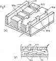
図1を参照すると、この図は本発明の実施例に係わる金属部品の製造における処理ステップを示す。図1(a)に示されるように、1つの物体の全体が番号102で表示されている。この場合、この物体は上部表面106を有する、金属、例えばアルミニウムまたはスチール(もしくは金もしくはルテニウムのような金属でコーティングすることが適当な場合はセラミック)で形成された基板、すなわちベース層104を含む。しかしながら、所定の実施例では、この物体は異形マンドレル、雌型または別の特徴部を追加すべき、現存する機械的な部品でよい。例えば凹状の放物反射面を有する光学的望遠鏡のミラーの製造にあたり、以下、より詳細に説明するような一体的な冷却/熱交換チャンネルを備えた1つ以上の層を含む(例えば最初の反射層を含む)1つ以上の金属層が形成された、適当に研磨された凸状の放物外側表面を有するようにマンドレルを成形できる。
Referring to FIG. 1, this figure shows processing steps in the manufacture of a metal part according to an embodiment of the present invention. As shown in FIG. 1A, the whole of one object is displayed by the
図1(b)を参照する。基板104の上部表面106上に第1金属層108をデポジットするように、最初の電鋳作業を実行する。当業者にはこの電鋳技術は周知であるので、説明を簡潔にするためにこの技術の詳細については繰り返して説明しない。第1金属層108の金属は、ニッケル、銅または電鋳に適したその他の任意の金属でよい。この電鋳作業にかかる時間は必要とされる第1金属層108の厚みt1に応じて決まる。この層は100〜200μmの厚さでもよいし、ある値のミリメートルでもよいが、特定の用途または製造すべき部品に応じてこの値よりも厚くてもよいし、薄くてもよい。
Reference is made to FIG. An initial electroforming operation is performed to deposit a
このステップの後に、第1金属層108の頂部表面110に第1マスク層112を形成するステップ(図1(c))が続く。この第1マスク層112は当業者に周知のようにポリマーシートを接着(糊付け)することによって適当に形成される(もしくは溶解した、または溶融された材料をキャストすることによって形成してもよい)。この第1マスク層112は、低融点材料、例えばPMMAを適当に含むが、その他の材料も使用できる。第1マスク層112は用途に応じて種々の厚み(t2)に形成できる。この厚みは1mmまたは2mmでもよいし、例えば第1金属層108の大きさ、もしくはその厚みt1よりも厚くてもよい。
This step is followed by the step of forming a
次に精密フライス加工機械または旋盤を使って第1マスク層112にパターンを形成すると、その結果、図1(d)に示される製品が得られる。この方法と異なり、レーザーカッティング装置または光学的リソグラフィプロセスを使用できる。このパターン形成ステップは選択された領域で、第1金属層108の表面110よりも上にある第1マスク層112の材料を除去し、(図1(d)内の紙内まで延びる)細長い第1リセス114を発生する。この細長い第1リセス114の幅(w1)は用途に応じて大きく変わることができ、例えば第1マスク層112の厚みt2の0.5〜1.0倍でよい。しかしながら、この幅は、(a)機械加工により数百μm以上(例えば約300μmより大)とするか、(b)レーザーカッティングにより(例えば約20μmよりも大きい)数十μmとするか、(c)リソグラフィにより(例えば約1μmよりも大きい)数μmとすることができる。幅に関する上限は正当な範囲内の任意の値、例えば数センチメートルまでの数mmとなり得る。
Next, when a pattern is formed on the
その後、第2の電鋳作業を実行する。この作業は第1電鋳と同じ金属(ニッケル)を使って適当に行うことができるが、異なる材料を使用してもよい。図1(e)に示されるように、この第2電鋳作業は第1の細長いリセス114が完全に電鋳金属で満たされる程度まで実行され、金属は一般にオーバーフローし、膨張部118を一般に形成する。この膨張部は、融合し、t3で示される最も狭いポイントにおいて所定の厚みを有する凹凸のある上部金属層120を形成する。
Thereafter, a second electroforming operation is performed. This operation can be suitably performed using the same metal (nickel) as in the first electroforming, but a different material may be used. As shown in FIG. 1 (e), this second electroforming operation is performed to the extent that the first
次に電子的に制御された適当な工作機械を使って、凹凸のある上部金属層120を機械加工し、図1(f)に示されるように、フラットまたは実質的に平らな上部表面122を形成する。従って、厚みt4(ここでt4≦t3である)を有する第2金属層124が形成される。一般にt4=t1であるが、用途によってはt4<t1またはt4>t1とすることも可能である。この段階において、基板104に付着し、一連の細長い第1チャンネル126を有する平行な外側層を有する金属構造が生じ、チャンネルは第1側壁128によって分離され、ポリマー(PMMA)で充填されている。この場合に、側壁128の表面130は平らである。この中間生成物を更に処理する方法は、数種の形態をとり得る。
A suitable electronically controlled machine tool is then used to machine the uneven
図2は本発明の第1実施例に係わる、全体が番号200で表示された第1タイプの金属部品を製造する技術を示す。ここで図1(a)〜(f)の処理の後で、適当な高温にて(例えばオーブン内にて)溶融するか、または適当な(例えば有機)溶剤、例えばクロロフォルム内で溶解することによって、基板100の材料および細長い第1チャンネル126内のポリマーを除去する。部品200は、平行な表面122、202を有し、これら表面を貫通する一連の細長い空の第1チャンネル126を有する。基板が金属基板である場合、一般に機械的な分離によってこの基板を除去する。
FIG. 2 shows a technique for manufacturing a first type metal part, generally designated by the numeral 200, according to the first embodiment of the present invention. Here, after the treatment of FIGS. 1 (a)-(f), by melting at a suitable high temperature (eg in an oven) or by dissolving in a suitable (eg organic) solvent, eg chloroform. The substrate 100 material and the polymer in the elongated
部品200は、平坦な構造を有するように示されているが、当業者であれば、プロセスの開始時に使用される物体またはマンドレルの形状に応じて球形、円錐形、放物形、双曲線形などの構造またはその一部を形成してもよい。
Although
図3は、本発明の第2実施例に係わる、全体が番号300で表示された第2タイプの金属部品を製造する技術を示す。このプロセスは以下に説明することを除けば、第1実施例と同じでよい。この場合、図1(f)に示される時点の後で、このステップの後に第2金属層124の頂部表面上に第2マスク層を形成する。この第2マスク層112は当業者に公知のようにポリマーシートを接着(糊付け)することによって適当に形成される(もしくは溶解された材料をキャストするか、または溶融することによって第2マスク層112を形成してもよい)。この第2マスク層112は低溶融点材料、例えばPMMAを適当に含むが、他の材料を使用してもよい。用途によってはこの第2マスク層12を種々の厚み(t5)に形成してもよい。このマスク層は1mmまたは2mmの大きさとするか、または例えば第1金属層108の厚みt1または第2金属層124の厚みt4の大きさ、もしくはそれよりも大きくすることができる。
FIG. 3 shows a technique for manufacturing a second type metal part, generally designated by the numeral 300, according to a second embodiment of the present invention. This process may be the same as the first embodiment except as described below. In this case, a second mask layer is formed on the top surface of the
次に、精密フライス切削機械または旋盤を使って第2マスク層のパターン形成を行い、その結果、図1(d)に示される形状に類似した形状が得られる。この方法とは異なり、レーザーカッティング機械または光学的リソグラフィプロセスを使用することもできる。このパターン形成ステップは選択された領域にある、第2金属層124の表面122よりも上にある第2マスク層材料を除去し(図1の紙内まで延びる)細長い第2リセスを形成する。用途によっては細長い第2リセスの幅w2は大きく変化でき、例えば第2マスク層112の厚みt5の0.5〜1.5倍とすることができる。しかしながら、この幅は(a)機械加工により数百μm以上(例えば約300μmより大)とするか、(b)レーザーカッティングにより(例えば約20μmよりも大きい)数十μmとするか、(c)リソグラフィにより(例えば約1μmよりも大きい)数μmとすることができる。幅に関する上限は正当な範囲内の任意の値、例えば数センチメートルまでの数mmとなり得る。
Next, patterning of the second mask layer is performed using a precision milling machine or a lathe, and as a result, a shape similar to the shape shown in FIG. Unlike this method, a laser cutting machine or an optical lithography process can be used. This patterning step removes the second mask layer material above the
前と同じように、フラットまたは実質的に平らな上部表面122を形成するように電子的に制御された適当な工作機械を使って、凹凸のある上部金属層120を機械加工する。従って、厚みt4(ここでt4≦t3である)を有する第2金属層124が形成される。一般にt4=t1であるが、用途によってはt4<t1またはt4>t1とすることも可能である。この段階において、基板104に付着し、一連の細長い第1チャンネル126を有する平行な外側層を有する金属構造が生じ、チャンネルは第1側壁128によって分離され、ポリマー(PMMA)で充填されている。この場合に、側壁128の表面130は平らである。
As before, the uneven
この結果、図3の構造が得られる。この構造から、前と同じように(ここでは平行な)細長い第1チャンネル126および細長い第2チャンネル306を有する物体(基板、マンドレル)を除去することができ、これらチャンネルを使って(これらに流体を流すことにより)部品300の熱交換/冷却を行うことができる。
As a result, the structure of FIG. 3 is obtained. From this structure, an object (substrate, mandrel) having an elongated
図4は本発明の第3実施例に係わる、全体が番号400で示された第3タイプの金属部品を製造する技術を示す。ここで、このプロセスは図3の実施例を同じであるが、形成されるリセス、従ってその結果生じる細長い第2チャンネル306が、細長い第1チャンネル126の方向に対して横方向(すなわち90度であるが、その他の適当な角度を使用することもできる)に延びるように第2マスク層のパターン形成が行われている点が異なっている。この構造は熱交換システム、例えばクロスフロータイプの熱交換器に特定の用途がある。すなわち、ここでは、各ケースにおいて、例えば適当なポンピングまたは対流により細長い第1チャンネル126を高温の流体が通過し、細長い第2チャンネル306を低温流体が通過する。このケースでは、部品400は、銅から適当に製造する。
FIG. 4 shows a technique for manufacturing a third type metal part, generally designated by reference numeral 400, according to a third embodiment of the present invention. Here, this process is the same as in the embodiment of FIG. 3, but the recess formed and thus the resulting elongated
図5は本発明の第4実施例に係わる、全体が番号500で示された第4タイプの金属部品を製造する技術を示す。このプロセスは、図3を参照して説明したプロセスと同じであるが、基板104上の二次元状第1領域(例えば正方形)上に第1金属層108および第2金属層112が製造されている点が異なる。しかしながら、第3金属層124、第2マスク層(図示せず)および第3金属層304は、二次元状第1領域よりも大きい二次元状第2領域の上に製造されている。このようにオーバーラップし、横方向となるか、または三次元状に延び得る(矢印A、Bによって表示された)流体流を形成することができる。
FIG. 5 shows a technique for manufacturing a fourth type metal part, generally designated by the numeral 500, according to a fourth embodiment of the present invention. This process is the same as that described with reference to FIG. 3 except that the
図6は、本発明の第5実施例に係わる、全体が番号600で表示された第5タイプの金属部品を製造する技術を示す。この技術は高強度が必要とされる比較的薄肉部品を製造するのに使用される。この場合、このプロセスは図2を参照して説明したプロセスと同じであるが、長時間にわたって第2電鋳作業を実行する点が異なっている。この結果、第2金属層124の厚みt4は第1金属層108の厚みt1よりも厚くなり、例えば細長い第1チャンネル126の厚みt2の1〜2倍となる。例えば厚みt4は部品の用途に応じて1〜2mmから1〜2cm、またはそれ以上のいずれかとなり得る。当業者であれば理解できるように、逆の構造にすることも可能である。すなわち第1金属層108の厚みt1のほうが、同じように第2金属層124の厚みt4よりも厚くなっている構造とすることもできる。これとは異なり、第1金属層と第2金属層124の双方の厚みを厚くすることもできる。
FIG. 6 shows a technique for manufacturing a fifth type metal part, generally designated by the numeral 600, according to a fifth embodiment of the present invention. This technique is used to produce relatively thin parts that require high strength. In this case, this process is the same as the process described with reference to FIG. 2, except that the second electroforming operation is performed for a long time. As a result, the thickness t4 of the
図7は本発明の別の実施例に従いマスク層またはその各々に対して行うことができるパターン形成を示す。長さ方向に沿って横断面の寸法が均一なリセス114を形成するために、マスク層114を切断するだけでなく、長さ方向に沿って幅が増減するようにリセス114’をカットすることもできる。リセス114’の一端702を他端704よりも狭くすることは、最終的に製造される細長いチャンネルが、その長手方向に沿って太いか、または細くなっている寸法を有し得ることを意味する。長手方向に沿って太くなったチャンネルにより、流体が流れるにつれて好ましく膨張でき、冷却/熱交換レートを増すこともできる。
FIG. 7 illustrates the patterning that can be performed on the mask layer or each of them according to another embodiment of the present invention. In order to form a
図8(a)は本発明の別の実施例に係わるマスク層またはその各々に対して実行できるパターン形成を示す。ここで通常のリセス114を製造するだけでなく、頂部リセス804を形成するために、頂部表面802上にマスク層のパターン形成(カット)を行い、サイドリセス808を形成するためにサイド表面806上でパターン形成できる。これによって最終的に製造される細長いチャンネルの側壁(130、308)の構造に影響がおよぶ。図8(b)にはこの影響が示されている。側壁130は矢印によって表示されるように、使用時に複雑な流体の流れを発生させるバッフル810を有する。かかる複雑な直線状でない流れは冷却/熱交換効率を高めるのを更に補助できる。
FIG. 8 (a) shows the patterning that can be performed on the mask layer or each of them according to another embodiment of the present invention. Here, in addition to manufacturing the
本発明の有利な使用の一例として、極短波長紫外線(EUV)システムで使用される光学的部品の製造を挙げることができる。かかるシステムで使用される光学部品(例えばミラー)は、一般に真空チャンバ内のEUV放射線源(例えばプラズマソース)に沿って収納される。リソグラフ用に使用されるEUV光源の一例は、100Wまたはそれ以上の比較的高い光学パワーで13.4nmの波長のEUV放射線を発生する。プラズマソースは一般にミラーのような隣接部品をかなり加熱させる波長を含む波形/波長の所定のレンジ内のエネルギーを一般に放出する。これまでは(例えば空気対流による)冷却は行われず、ミラーの過熱によってミラー表面にかなりの欠陥が生じ、このことはシステムの性能に有害な影響を与え得る。 One example of an advantageous use of the present invention is the manufacture of optical components used in very short wavelength ultraviolet (EUV) systems. Optical components (eg, mirrors) used in such systems are typically housed along an EUV radiation source (eg, a plasma source) in a vacuum chamber. An example of an EUV light source used for lithography generates EUV radiation with a wavelength of 13.4 nm with a relatively high optical power of 100 W or higher. The plasma source typically emits energy within a predetermined range of waveforms / wavelengths, including wavelengths that generally heat adjacent components such as mirrors. To date, no cooling has occurred (e.g., by air convection) and mirror overheating can cause significant defects on the mirror surface, which can have a detrimental effect on system performance.
本発明の適当な実施例に係わる製造技術を使ってこの影響を解消または低減できる。ここで、部品の所望する最終形状(例えば楕円形、放物形;例えばリソグラフィ用には50mm〜200mmの大きさ)のネガ形状を有するマンドレル(例えばガラス)に真空蒸着によりEUVエネルギーの反射に適した材料、例えばルテニウムをまずコーティングする。次に、本発明に係わる上記技術によりルテニウム層上にミラーの残りの部分を(例えばニッケルで)形成する。従ってこのニッケルは冷却チャンネルの1つ以上の層を含む。こうして形成されたミラーは1〜数mmの厚み、例えば2mmの厚みとなり得る。マンドレルからミラー(ニッケル+ルテニウム層)を機械的に除去し、実質的な別の加工または処理をすることなく、一般にすぐに実装/使用が可能である。 This effect can be eliminated or reduced using manufacturing techniques according to suitable embodiments of the present invention. Here, suitable for reflection of EUV energy by vacuum deposition on a mandrel (eg glass) having a negative shape of the desired final shape of the part (eg oval, parabolic; eg 50 mm to 200 mm in size for lithography) A material such as ruthenium is first coated. Next, the remaining part of the mirror is formed (for example with nickel) on the ruthenium layer by the above technique according to the present invention. The nickel thus includes one or more layers of cooling channels. The mirror thus formed can be 1 to several mm thick, for example 2 mm thick. The mirror (nickel + ruthenium layer) is mechanically removed from the mandrel and can generally be implemented / used immediately without substantial further processing or processing.
使用に際し、ミラー内に内在させたチャンネルのシステムに冷却流体(例えば水)を通過させることによってミラーを冷却流体できる。作動温度が数千度にも達し得る他の用途(例えばロケットエンジン)と異なり、ミラーは数百度(例えば一般に300度)の温度で作動し得る。この温度は(他の温度と比較して)極端に高い温度ではないので、ニッケル層内の冷却チャンネルの横断面の寸法はこれに対応してより小さく、すなわちμmの大きさ、例えば1〜2μmにすることができる。 In use, the mirror can be cooled by passing a cooling fluid (e.g., water) through a system of channels contained within the mirror. Unlike other applications (e.g., rocket engines) where the operating temperature can reach several thousand degrees, the mirror can operate at a temperature of several hundred degrees (e.g., typically 300 degrees). Since this temperature is not extremely high (compared to other temperatures), the cross-sectional dimension of the cooling channel in the nickel layer is correspondingly smaller, i.e. in the order of [mu] m, e.g. 1-2 [mu] m. Can be.
しかしながら、当業者であれば、本発明は本明細書に説明した多数の工業的用途だけでなく、本明細書で言及しなかった他の用途にも適用できることが理解できよう。更に、個々の実施例に関連して所定の技術、プロセスのステップ、材料および寸法について説明したが、かかる技術、プロセスのステップ、材料および寸法は、適当に組み合わせて使用することができるし、および/または特定の用途に合わせて変えることができると理解できよう。 However, those skilled in the art will appreciate that the present invention is applicable not only to the numerous industrial applications described herein, but also to other applications not mentioned herein. Furthermore, although certain techniques, process steps, materials and dimensions have been described in connection with individual embodiments, such techniques, process steps, materials and dimensions can be used in any suitable combination, and It will be appreciated that it can be varied for specific applications.
102 物体
104 基板
106 上部表面
108 第1金属層
110 頂部表面
112 第1マスク層
114 リセス
116 電鋳金属
126 チャンネル
102
Claims (15)
第1電鋳作業を実行し、前記表面に金属材料を備えた第1金属層を形成するステップと、
非導電性材料を含む第1マスク層を前記第1金属層上に形成するステップと、
前記第1マスク層にパターン形成し、第1金属層よりも上の前記非導電性材料を除去した、細長い寸法の複数の第1リセスを前記第1マスク層に設けるステップと、
前記金属材料を使って第2電鋳作業を実行し、前記第1リセスに前記金属材料を充填し、前記第1マスク層よりも上にあって、前記第1マスク層の表面全体またはその一部を覆い、少なくとも第1の所定の厚みに延び、前記金属材料を含む第2金属層を形成するステップと、
前記第1マスク層を溶かして前記第1金属層上から除去するステップと、
前記第2金属層を機械加工し、均一な厚みの第2金属層を形成するステップを備え、よって前記第2金属層が上部表面を有し、
さらに、
非導電性材料を含む第2マスク層を前記第2金属層上に形成するステップと、
前記第2マスク層にパターン形成し、第2金属層よりも上の前記非導電性材料を除去した、細長い寸法の複数の第2リセスを前記第2マスク層に設けるステップと、
前記金属材料を使って第3電鋳作業を実行し、前記第2リセスに前記金属材料を充填し、少なくとも第2の所定の厚みに延び、前記第2マスク層の表面全体またはその一部を覆う、前記金属材料を含む第3金属層を形成するステップと、
前記第3金属層を機械加工し、均一な厚みの第3金属層を形成するステップを備え、よって前記第3金属層が上部表面を有し、
さらに、
物体を除去すると共に前記第1マスク層および前記第2マスク層の非導電性材料を除去し、よって前記第1マスク層の非導電性材料が除かれた内部に延びる細長い第1チャンネルを有すると共に、前記第2マスク層の非導電性材料が除去された、内部に延びる細長い第2チャンネルを有する金属製部品を製造するステップとを備え、
第1金属層、第1マスク層および第2金属層が所定の二次元状第1領域を覆って延びるように、第1電鋳作業を実行するステップ、第1マスク層を形成するステップ、前記第1マスク層にパターン形成するステップ、および第2電鋳を実行するステップを実行し、
第2金属層、第2マスク層および第3金属層が所定の二次元状第2領域を覆って延びるように第2マスクを形成するステップ、前記第2マスク層にパターン形成するステップ、および第3電鋳作業を実行するステップを実行し、
前記二次元状第2領域を前記二次元状第1領域よりも広くする、金属部品を製造するための方法。Providing an object having a surface;
Performing a first electroforming operation and forming a first metal layer comprising a metal material on the surface;
Forming a first mask layer comprising a non-conductive material on the first metal layer;
Providing the first mask layer with a plurality of elongate first recesses patterned on the first mask layer and removing the non-conductive material above the first metal layer;
A second electroforming operation is performed using the metal material, the first recess is filled with the metal material, and the entire surface of the first mask layer or a part thereof is above the first mask layer. Forming a second metal layer that covers the portion and extends to at least a first predetermined thickness and includes the metal material;
Removing from said first metal layer by dissolving said first mask layer,
Machining the second metal layer to form a second metal layer of uniform thickness, so that the second metal layer has an upper surface;
further,
Forming a second mask layer comprising a non-conductive material on the second metal layer;
Providing the second mask layer with a plurality of elongated recesses having a pattern formed in the second mask layer and removing the non-conductive material above the second metal layer;
A third electroforming operation is performed using the metal material, the second recess is filled with the metal material, extends to at least a second predetermined thickness, and the entire surface of the second mask layer or a part thereof is formed. Forming a third metal layer comprising the metal material to cover,
Machining the third metal layer to form a third metal layer of uniform thickness, so that the third metal layer has an upper surface;
further,
And having an elongated first channel extending into the interior of the first mask layer to remove non-conductive material and thereby remove the non-conductive material of the first mask layer and the second mask layer. Manufacturing a metal part having an elongated second channel extending therein, wherein the non-conductive material of the second mask layer has been removed,
Performing a first electroforming operation such that the first metal layer, the first mask layer, and the second metal layer extend over a predetermined two-dimensional first region, forming the first mask layer, Performing the steps of patterning the first mask layer and performing the second electroforming;
Forming a second mask such that the second metal layer, the second mask layer, and the third metal layer extend over a predetermined two-dimensional second region, patterning the second mask layer, and 3 execute the step of performing electroforming work,
A method for manufacturing a metal part , wherein the two-dimensional second region is wider than the two-dimensional first region .
(b)前記細長い第1チャンネルのほうが前記細長い第2チャンネルよりも幅が広いか、またはこの逆となるか、および/または
(c)前記細長い第1チャンネルおよび/または前記細長い第2チャンネルがそれぞれの延伸方向に沿って幅または厚みにテーパが付いており、および/または
(d)前記細長い第1チャンネルの延伸方向が前記細長い第2チャンネルの延伸方向に対して直角となっており、および/または
(e)前記細長い第1チャンネルおよび/または前記細長い第2チャンネルには突起、側壁リセスおよび/またはバッフルが設けられ、よってかかるチャンネルを通過する直線状でない流れが得られるように、前記第1マスク層にパターン形成するステップおよび/または前記第2マスク層にパターン形成するステップを実行する、請求項1記載の方法。(A) the first recess is wider than the second recess, or vice versa, and / or (b) the elongated first channel is wider than the elongated second channel. And / or vice versa, and / or (c) the elongated first channel and / or the elongated second channel are tapered in width or thickness along their respective stretch direction, and / or (d) ) The direction of extension of the elongated first channel is perpendicular to the direction of extension of the elongated second channel, and / or (e) a protrusion on the elongated first channel and / or the elongated second channel; Side wall recesses and / or baffles are provided so that a non-linear flow through such channels is obtained. The method of claim 1 , wherein patterning on one mask layer and / or patterning on the second mask layer is performed.
Applications Claiming Priority (2)
| Application Number | Priority Date | Filing Date | Title |
|---|---|---|---|
| IT0300771 | 2003-11-25 | ||
| PCT/EP2004/013296 WO2005054547A2 (en) | 2003-11-25 | 2004-11-23 | Fabrication of cooling and heat transfer systems by electroforming |
Publications (2)
| Publication Number | Publication Date |
|---|---|
| JP2007512434A JP2007512434A (en) | 2007-05-17 |
| JP4584261B2 true JP4584261B2 (en) | 2010-11-17 |
Family
ID=34640334
Family Applications (1)
| Application Number | Title | Priority Date | Filing Date |
|---|---|---|---|
| JP2006540364A Expired - Fee Related JP4584261B2 (en) | 2003-11-25 | 2004-11-23 | Manufacturing of cooling and heat exchange system by electroforming |
Country Status (5)
| Country | Link |
|---|---|
| US (1) | US8061032B2 (en) |
| EP (1) | EP1692327A2 (en) |
| JP (1) | JP4584261B2 (en) |
| KR (1) | KR20060132625A (en) |
| WO (1) | WO2005054547A2 (en) |
Families Citing this family (26)
| Publication number | Priority date | Publication date | Assignee | Title |
|---|---|---|---|---|
| DE102005053415A1 (en) * | 2005-11-04 | 2007-05-10 | Carl Zeiss Laser Optics Gmbh | Optical component with improved thermal behavior |
| EP1835050A1 (en) | 2006-03-15 | 2007-09-19 | Doniar S.A. | Process for the fabrication of LIGA-UV multilayer metallic structures, the layers being adjacent and not completely superimposed, and structure therefrom. |
| US8831170B2 (en) | 2006-11-03 | 2014-09-09 | Carl Zeiss Smt Gmbh | Mirror with a mirror carrier and projection exposure apparatus |
| DE102007013162A1 (en) * | 2007-03-20 | 2008-09-25 | Groß, Heinz, Dr. Ing. | Forming process for the production of multifunctional components |
| GB0715979D0 (en) * | 2007-08-15 | 2007-09-26 | Rolls Royce Plc | Heat exchanger |
| EP2083328B1 (en) | 2008-01-28 | 2013-06-19 | Media Lario s.r.l. | Grazing incidence collector for laser produced plasma sources |
| DE102011010021A1 (en) * | 2011-02-02 | 2012-08-02 | Karlsruher Institut für Technologie | Cross flow heat exchanger |
| US8746975B2 (en) | 2011-02-17 | 2014-06-10 | Media Lario S.R.L. | Thermal management systems, assemblies and methods for grazing incidence collectors for EUV lithography |
| DE102011004446A1 (en) | 2011-02-21 | 2012-08-23 | Carl Zeiss Smt Gmbh | Optical element for optical device e.g. projection exposure apparatus, has optically active element that is formed from silicon, and cooling element that is formed of silicon carbide or siliconized silicon carbide |
| US9777384B2 (en) | 2011-04-05 | 2017-10-03 | The United States Of America, As Represented By The Secretary Of The Navy | Microfabrication of tunnels |
| US8731139B2 (en) | 2011-05-04 | 2014-05-20 | Media Lario S.R.L. | Evaporative thermal management of grazing incidence collectors for EUV lithography |
| FR2977017B1 (en) * | 2011-06-27 | 2015-05-01 | Commissariat Energie Atomique | HEAT REGENERATOR |
| CN103502765A (en) * | 2011-10-19 | 2014-01-08 | 松下电器产业株式会社 | Heat exchanger |
| JP2016530140A (en) * | 2013-09-19 | 2016-09-29 | トレデガー フィルム プロダクツ コーポレイション | Method for making a molding screen |
| WO2016017697A1 (en) * | 2014-07-29 | 2016-02-04 | 京セラ株式会社 | Heat exchanger |
| TWI556376B (en) * | 2015-08-28 | 2016-11-01 | 國立交通大學 | Heat conducting module |
| CN107523856B (en) * | 2016-06-17 | 2020-11-06 | 通用电气公司 | System and method for processing workpiece and product |
| US11091848B2 (en) * | 2017-05-11 | 2021-08-17 | Unison Industries, Llc | Component with differing material properties |
| US20180328285A1 (en) * | 2017-05-11 | 2018-11-15 | Unison Industries, Llc | Heat exchanger |
| US10900136B2 (en) * | 2017-07-18 | 2021-01-26 | Honeywell International Inc. | Additive-based electroforming manufacturing methods and metallic articles produced thereby |
| US10927711B2 (en) | 2017-10-26 | 2021-02-23 | Unison Industries, Llc | Tunable compliant attachment structure |
| US11686012B2 (en) | 2017-10-26 | 2023-06-27 | Unison Industries, Llc | Mandrel for electroforming |
| US11078795B2 (en) | 2017-11-16 | 2021-08-03 | General Electric Company | OGV electroformed heat exchangers |
| CN108070883B (en) * | 2017-12-07 | 2019-09-17 | 天津大学 | A method of pure nanometer cobalt array is prepared based on anodic oxidation aluminium formwork method |
| US20220282391A1 (en) * | 2021-03-04 | 2022-09-08 | Unison Industries, Llc | Additive heat exchanger and method of forming |
| JP2023051451A (en) * | 2021-09-30 | 2023-04-11 | 富士フイルム株式会社 | Electroforming method and manufacturing method for electroformed product |
Family Cites Families (9)
| Publication number | Priority date | Publication date | Assignee | Title |
|---|---|---|---|---|
| US4205428A (en) * | 1978-02-23 | 1980-06-03 | The United States Of America As Represented By The Secretary Of The Air Force | Planar liquid crystal matrix array chip |
| IL70146A0 (en) * | 1982-12-22 | 1984-02-29 | Gen Electric | Article with a fluid passage and method for making it |
| FR2567684B1 (en) * | 1984-07-10 | 1988-11-04 | Nec Corp | MODULE HAVING A MULTILAYER CERAMIC SUBSTRATE AND A MULTILAYER CIRCUIT ON THE SUBSTRATE AND METHOD FOR THE PRODUCTION THEREOF |
| JPH0821567B2 (en) | 1985-03-14 | 1996-03-04 | 富士通株式会社 | Ultrafine tube manufacturing method |
| JPH06101616B2 (en) * | 1986-02-21 | 1994-12-12 | 名幸電子工業株式会社 | Method for manufacturing conductor circuit board |
| JPH0634283A (en) * | 1992-06-16 | 1994-02-08 | Ishikawajima Harima Heavy Ind Co Ltd | Manufacture of heat exchanger for use in space |
| DE19920161A1 (en) | 1998-11-06 | 2000-05-25 | Atotech Deutschland Gmbh | Process for the production of micro components with flow channels |
| US6602053B2 (en) * | 2001-08-02 | 2003-08-05 | Siemens Westinghouse Power Corporation | Cooling structure and method of manufacturing the same |
| WO2003049514A2 (en) * | 2001-12-03 | 2003-06-12 | Memgen Corporation | Miniature rf and microwave components and methods for fabricating such components |
-
2004
- 2004-11-23 EP EP04819613A patent/EP1692327A2/en not_active Withdrawn
- 2004-11-23 WO PCT/EP2004/013296 patent/WO2005054547A2/en active Application Filing
- 2004-11-23 US US10/580,397 patent/US8061032B2/en not_active Expired - Fee Related
- 2004-11-23 KR KR1020067012465A patent/KR20060132625A/en not_active Application Discontinuation
- 2004-11-23 JP JP2006540364A patent/JP4584261B2/en not_active Expired - Fee Related
Also Published As
| Publication number | Publication date |
|---|---|
| WO2005054547A2 (en) | 2005-06-16 |
| US8061032B2 (en) | 2011-11-22 |
| JP2007512434A (en) | 2007-05-17 |
| KR20060132625A (en) | 2006-12-21 |
| EP1692327A2 (en) | 2006-08-23 |
| US20070134908A1 (en) | 2007-06-14 |
| WO2005054547A3 (en) | 2005-11-24 |
Similar Documents
| Publication | Publication Date | Title |
|---|---|---|
| JP4584261B2 (en) | Manufacturing of cooling and heat exchange system by electroforming | |
| JP6636575B2 (en) | Additive manufacturing heat exchanger | |
| JP7040707B2 (en) | Additional manufactured heat exchanger | |
| EP1824629B1 (en) | Heat exchanger | |
| JP7079281B2 (en) | Methods for Manufacturing Catoptrics, Use of Catoptrics and Catoptrics | |
| US11193716B2 (en) | Fluid routing methods for a spiral heat exchanger with lattice cross section made via additive manufacturing | |
| US20170059256A1 (en) | Net-shape structure with micro-truss core | |
| US11248491B2 (en) | Additively deposited gas turbine engine cooling component | |
| US20180297843A1 (en) | Cell structures for use in heat exchangers, and methods of producing the same | |
| WO2008079593A2 (en) | Method of using minimal surfaces and minimal skeletons to make heat exchanger components herewith | |
| JP5864091B2 (en) | Cooling system and method for grazing incidence EUV lithography concentrator | |
| Saxena et al. | High-speed fabrication of microchannels using line-based laser induced plasma micromachining | |
| Arias et al. | Fabrication of metallic heat exchangers using sacrificial polymer mandrils | |
| EP3054253B1 (en) | Heat exchanger article with hollow tube having plurality of vanes | |
| Brandner et al. | Comparison of crossflow micro heat exchangers with different microstructure designs | |
| Tsopanos et al. | Manufacturing novel heat transfer devices by selective laser melting | |
| Kelly et al. | Very Deep X-Ray Lithography for Heat and Mass Transfer Applications | |
| Kelly et al. | High Performance Micro-Channel Cross Flow Heat Exchangers |
Legal Events
| Date | Code | Title | Description |
|---|---|---|---|
| A621 | Written request for application examination |
Free format text: JAPANESE INTERMEDIATE CODE: A621 Effective date: 20070914 |
|
| A977 | Report on retrieval |
Free format text: JAPANESE INTERMEDIATE CODE: A971007 Effective date: 20091029 |
|
| A131 | Notification of reasons for refusal |
Free format text: JAPANESE INTERMEDIATE CODE: A131 Effective date: 20091116 |
|
| A521 | Request for written amendment filed |
Free format text: JAPANESE INTERMEDIATE CODE: A523 Effective date: 20100216 |
|
| A131 | Notification of reasons for refusal |
Free format text: JAPANESE INTERMEDIATE CODE: A131 Effective date: 20100405 |
|
| A521 | Request for written amendment filed |
Free format text: JAPANESE INTERMEDIATE CODE: A523 Effective date: 20100705 |
|
| TRDD | Decision of grant or rejection written | ||
| A01 | Written decision to grant a patent or to grant a registration (utility model) |
Free format text: JAPANESE INTERMEDIATE CODE: A01 Effective date: 20100802 |
|
| A01 | Written decision to grant a patent or to grant a registration (utility model) |
Free format text: JAPANESE INTERMEDIATE CODE: A01 |
|
| A61 | First payment of annual fees (during grant procedure) |
Free format text: JAPANESE INTERMEDIATE CODE: A61 Effective date: 20100901 |
|
| R150 | Certificate of patent or registration of utility model |
Ref document number: 4584261 Country of ref document: JP Free format text: JAPANESE INTERMEDIATE CODE: R150 Free format text: JAPANESE INTERMEDIATE CODE: R150 |
|
| FPAY | Renewal fee payment (event date is renewal date of database) |
Free format text: PAYMENT UNTIL: 20130910 Year of fee payment: 3 |
|
| R250 | Receipt of annual fees |
Free format text: JAPANESE INTERMEDIATE CODE: R250 |
|
| R250 | Receipt of annual fees |
Free format text: JAPANESE INTERMEDIATE CODE: R250 |
|
| R250 | Receipt of annual fees |
Free format text: JAPANESE INTERMEDIATE CODE: R250 |
|
| R250 | Receipt of annual fees |
Free format text: JAPANESE INTERMEDIATE CODE: R250 |
|
| R250 | Receipt of annual fees |
Free format text: JAPANESE INTERMEDIATE CODE: R250 |
|
| R250 | Receipt of annual fees |
Free format text: JAPANESE INTERMEDIATE CODE: R250 |
|
| R250 | Receipt of annual fees |
Free format text: JAPANESE INTERMEDIATE CODE: R250 |
|
| R250 | Receipt of annual fees |
Free format text: JAPANESE INTERMEDIATE CODE: R250 |
|
| R250 | Receipt of annual fees |
Free format text: JAPANESE INTERMEDIATE CODE: R250 |
|
| LAPS | Cancellation because of no payment of annual fees |