JP4577156B2 - Electroless nickel plating bath and electroless plating method using the same - Google Patents
Electroless nickel plating bath and electroless plating method using the same Download PDFInfo
- Publication number
- JP4577156B2 JP4577156B2 JP2005245612A JP2005245612A JP4577156B2 JP 4577156 B2 JP4577156 B2 JP 4577156B2 JP 2005245612 A JP2005245612 A JP 2005245612A JP 2005245612 A JP2005245612 A JP 2005245612A JP 4577156 B2 JP4577156 B2 JP 4577156B2
- Authority
- JP
- Japan
- Prior art keywords
- electroless
- plating
- nickel plating
- film
- bath
- Prior art date
- Legal status (The legal status is an assumption and is not a legal conclusion. Google has not performed a legal analysis and makes no representation as to the accuracy of the status listed.)
- Expired - Fee Related
Links
Images

Description
本発明は、銅電極の上に直接無電解めっきできる無電解ニッケルめっき浴およびそれを用いた無電解めっき方法に関し、より詳しくはパラジウムなどの活性化触媒を用いないでプリント配線板に形成された銅電極の上に直接無電解めっき処理を施してニッケルめっき膜を形成する無電解ニッケルめっき浴およびそれを用いた無電解めっき方法に関するものである。 The present invention relates to an electroless nickel plating bath that can be electrolessly plated directly on a copper electrode and an electroless plating method using the same, and more specifically, formed on a printed wiring board without using an activation catalyst such as palladium. The present invention relates to an electroless nickel plating bath for forming a nickel plating film by directly performing electroless plating treatment on a copper electrode, and an electroless plating method using the same.
被めっき物の表面にニッケルめっき膜を被着形成させる手段としては、従来、電解めっき法と無電解めっき法が広く用いられ、特に無電解めっき法は、均一な厚みのめっき膜を容易に形成することができること、被めっき物を保持する治具等にめっき用電力を供給する手段を講じる必要がないこと、及び独立配線電極のみに選択的にめっき可能であることから多用されている。 Conventionally, electrolytic plating and electroless plating methods have been widely used as means for depositing and forming a nickel plating film on the surface of an object to be plated. In particular, the electroless plating method easily forms a plating film with a uniform thickness. It is frequently used because it is not necessary to provide means for supplying power for plating to a jig or the like for holding an object to be plated, and that only independent wiring electrodes can be selectively plated.
通常、絶縁樹脂基板であるプリント配線板の銅電極の上には無電解ニッケルめっき、無電解金めっきが施されており、このニッケルめっきは、銅の金めっき膜への拡散を防止する目的で、金めっき処理を施す前に次亜リン酸塩を還元剤とした無電解ニッケルめっきを施し、耐食性に優れたニッケル−P膜を形成しており、さらに金めっきは、はんだ付け性やワイヤーボンディング性を向上させる観点から電極表面に形成されている。 Usually, electroless nickel plating and electroless gold plating are applied on the copper electrode of the printed wiring board, which is an insulating resin substrate. This nickel plating is used to prevent diffusion of copper into the gold plating film. Electroless nickel plating with hypophosphite as a reducing agent is applied before gold plating treatment to form a nickel-P film with excellent corrosion resistance. Furthermore, gold plating is used for solderability and wire bonding. From the viewpoint of improving the property, it is formed on the electrode surface.
そして、この種のめっき反応を生じさせるためには、電極材料が還元剤の酸化反応に対して触媒活性を有している必要があるが、銅は還元剤としての次亜リン酸塩の酸化反応に対し触媒活性度が低く、直接的にはニッケル−P膜の析出が生じ難いことから、電極の表面にパラジウム触媒を付与して電極の表面を触媒活性化した後、無電解ニッケルめっきを施している。 In order to cause this type of plating reaction, the electrode material needs to have catalytic activity for the oxidation reaction of the reducing agent, but copper is an oxidation of hypophosphite as the reducing agent. Since the catalytic activity for the reaction is low and it is difficult for nickel-P film to be deposited directly, after applying the palladium catalyst to the surface of the electrode to activate the surface of the electrode, electroless nickel plating is performed. Has been given.
しかしながら、近年益々ファインパターン化が進み、銅電極の導体間隔が狭くなってきており、銅電極の導体パターン以外の部分にもニッケルめっきが異常析出し、導体間の短絡等の不良が発生し易くなってきている。これは、銅電極の上にパラジウム触媒を付与する際、銅電極以外の箇所にもパラジウムが物理的に吸着するためであり、その結果、無電解ニッケルめっきを施した場合、銅電極以外の絶縁基板の上にもニッケル−P膜が析出してしまうという欠点があった。 However, in recent years, the finer pattern has been developed, and the conductor spacing of the copper electrodes has become narrower. Nickel plating has abnormally deposited on portions other than the conductor pattern of the copper electrodes, and defects such as short circuit between the conductors are likely to occur. It has become to. This is because when a palladium catalyst is applied on a copper electrode, palladium is physically adsorbed also at locations other than the copper electrode. As a result, when electroless nickel plating is applied, insulation other than the copper electrode is achieved. There was a drawback that the nickel-P film was deposited on the substrate.
そこで、その欠点を解消する方策として、従来より、ホウ素系化合物を還元剤として使用して無電解ニッケルめっきを施し、これにより銅電極の上にのみニッケル系めっき膜を形成する技術が提案されている。すなわち、従来技術では、ホウ素系化合物を還元剤として使用することにより、銅電極の表面にパラジウム触媒を付与することなく、直接的にニッケル−B膜を形成し、その後、該ニッケル−B膜の上にニッケル−Pめっき膜及び金めっき膜を順次形成している(例えば、特許文献1参照)。
しかしながら、前記従来の技術では、還元剤としてホウ素系化合物を使用することにより、パラジウム触媒を付与することなく電極の表面にのみめっき膜を形成することができるものの、銅はホウ素系化合物の酸化反応に対して触媒活性度が低いため、亜塩素酸化合物を含む酸化処理液で銅の表面を酸化して触媒活性化し、その後にめっき処理を行なう必要があり、このため、めっき工程数の複雑さを招くという問題点を有していた。 However, in the conventional technique, by using a boron compound as a reducing agent, a plating film can be formed only on the surface of the electrode without imparting a palladium catalyst, but copper is an oxidation reaction of the boron compound. Because of its low catalytic activity, it is necessary to oxidize the copper surface with an oxidation treatment solution containing a chlorite compound to activate the catalyst, and then perform plating treatment. Had the problem of inviting.
本発明は前記従来の課題を解決するもので、プリント配線板などの上に形成した銅電極へ、パラジウム触媒を付与することなく選択的に直接無電解ニッケルめっき膜の形成が可能な無電解めっき浴およびそれを用いた無電解めっき方法を提供することを目的とするものである。 The present invention solves the above-described conventional problems, and can form an electroless nickel plating film directly and selectively on a copper electrode formed on a printed wiring board or the like without providing a palladium catalyst. It is an object of the present invention to provide a bath and an electroless plating method using the same.
前記課題を解決するために、本発明は、酢酸ニッケルからなる金属供給源としてのニッケル塩と、還元剤としてのヒドラジンと、錯化剤としてのEDTAおよび乳酸と、pH緩衝剤としてのホウ酸とからなり、前記酢酸ニッケルを30.3〜35.4g/L、前記ヒドラジンを24.3〜48.6ml/L、前記乳酸を49.3〜61.6ml/L、前記EDTAを9.5〜19g/L、前記ホウ酸を24.8〜37.2g/Lの浴組成とした無電解ニッケルめっき浴とするものである。 In order to solve the above problems, the present invention includes a nickel salt as the metal source consisting of nickel acetate and hydrazine as a reducing agent, and EDTA and lactic acid as a complexing agent, and boric acid as a pH buffer The nickel acetate 30.3-35.4 g / L, the hydrazine 24.3-48.6 ml / L, the lactic acid 49.3-61.6 ml / L, and the EDTA 9.5 An electroless nickel plating bath having a bath composition of 19 g / L and 24.8-37.2 g / L of boric acid is used.
本発明による無電解ニッケルめっき浴とすることにより、高濃度のヒドラジンは単なる還元剤として作用するのではなく、銅電極の表面を活性化する高い触媒作用をも有していることから、プリント配線板などの上に形成した銅電極の上に、パラジウム触媒を付与することなく選択的に直接無電解ニッケルめっき膜の形成が可能な無電解めっき浴およびそれを用いた無電解めっき方法を実現することができる。 By using the electroless nickel plating bath according to the present invention, high concentration hydrazine does not act as a mere reducing agent but also has a high catalytic action to activate the surface of the copper electrode. An electroless plating bath capable of selectively forming an electroless nickel plating film directly on a copper electrode formed on a plate or the like without applying a palladium catalyst, and an electroless plating method using the same be able to.
(実施の形態1)
以下、本発明の実施の形態1における無電解ニッケルめっき浴およびそれを用いた無電解ニッケルめっき方法について、プリント配線板などに形成した銅電極の上に無電解めっき方法によって所定のめっき電極パターンを形成する方法を一例として図面を用いて説明する。
(Embodiment 1)
Hereinafter, regarding the electroless nickel plating bath and the electroless nickel plating method using the same in
図1は本発明の実施の形態1における無電解ニッケルめっき浴を用いて、プリント配線板の銅電極の上にめっき膜を形成する無電解めっき方法を説明するための断面図であり、図2は無電解めっき方法の処理手順を示す工程図である。
1 is a cross-sectional view for explaining an electroless plating method for forming a plating film on a copper electrode of a printed wiring board using the electroless nickel plating bath in
図1において、プリント配線板などでは絶縁樹脂1に不要な導体部分をエッチングするサブトラクティブ法により所定の配線パターンである銅電極2を形成し、さらにその上にフォトレジスト材料などを用いてレジストパターン3を露光、現像により形成している。
In FIG. 1, a
そして、銅電極2の表面には本実施の形態1における無電解ニッケルめっき浴を用いて、ニッケルめっき膜4が銅電極2の表面にパラジウム触媒を付与することなく選択的に形成されている。
Then, the nickel plating film 4 is selectively formed on the surface of the
また、このニッケルめっき膜4の表面には無電解めっきによる金めっき膜5が形成されている。このような構成の電極構造とすることによって半導体デバイスなどの実装性、接続信頼性に優れたプリント基板を実現することができる。
A
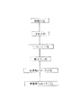
次に、以上のように構成されたプリント配線板への無電解めっきを用いた製造工程を図2を用いて説明する。 Next, a manufacturing process using electroless plating on the printed wiring board configured as described above will be described with reference to FIG.
まず始めに、テスト基板として厚さ0.6mmのガラスエポキシ基板(FR−4基材)を用い、電極幅(L)と電極間隔(S)とがL/S=50μm/50μmの配線パターンを有する銅電極2を形成した樹脂基板を用いた。
First, a glass epoxy substrate (FR-4 base material) having a thickness of 0.6 mm is used as a test substrate, and a wiring pattern having an electrode width (L) and an electrode interval (S) of L / S = 50 μm / 50 μm is used. A resin substrate on which the
そして、次の脱脂工程では、被めっき物であるテスト基板に付着した有機物質や無機物質による汚染を除去するとともに、無電解めっき液と銅電極2との濡れ性を向上させるべく、苛性ソーダなどを用いて被めっき物に酸性脱脂処理を施した。
Then, in the next degreasing process, caustic soda and the like are used in order to remove contamination due to organic substances and inorganic substances adhered to the test substrate as the object to be plated, and to improve the wettability between the electroless plating solution and the
次に、中和工程では酸性脱脂処理液に含まれる界面活性剤の除去を目的として、5%硫酸を用いて銅電極2の表面を清浄表面に戻した。
Next, in the neutralization step, the surface of the
その後、エッチング工程では、被めっき物を硫酸塩や過硫酸アンモニウム塩等の酸性水溶液に浸漬して銅電極2の表面に固着している酸化物をエッチング除去して表面形状の微調整を行った。
Thereafter, in the etching step, the object to be plated was immersed in an acidic aqueous solution such as sulfate or ammonium persulfate, and the oxide fixed to the surface of the
次に、酸活性工程では、銅電極2とめっき膜との密着性が向上するように、前記エッチング工程で銅電極2の表面に形成されたスマットを酸性処理液で除去した。
Next, in the acid activation step, the smut formed on the surface of the
次いで、無電解ニッケルめっき工程に進み、銅電極2の表面に本実施の形態1における無電解ニッケルめっき浴を用いて無電解ニッケルめっきを行い、ニッケルめっき膜4の平均膜厚が5μmになるように無電解ニッケルめっきを行った。
Next, the electroless nickel plating process is performed, and electroless nickel plating is performed on the surface of the
この無電解ニッケルめっきに用いためっき液は下記の無電解ニッケルめっき浴組成を有するニッケルめっき液を調製して使用した。 As the plating solution used for the electroless nickel plating, a nickel plating solution having the following electroless nickel plating bath composition was prepared and used.
[無電解ニッケルめっき浴組成の例]
酢酸ニッケル:35g/L
乳酸:62ml/L
EDTA:19g/L
ホウ酸:25g/L
ヒドラジン水和物:49ml/L
pH:11(水酸化ナトリウムで調整)
浴温:80℃
この無電解ニッケルめっき浴を用いて無電解ニッケルめっきを行うことによって銅電極2の表面のみに選択的にニッケルめっき膜4を製膜することが可能であった。特に、この無電解ニッケルめっき浴の特徴は銅電極2の表面のみにニッケルめっき膜4を選択的に形成することが可能となり、さらに無電解ニッケルめっき浴の組成を限定することによってニッケルめっき膜4の形成速度を11μm/hrという無電解めっきとしては高速のめっきレートで製膜できることを実現している。
[Example of electroless nickel plating bath composition]
Nickel acetate: 35 g / L
Lactic acid: 62ml / L
EDTA: 19g / L
Boric acid: 25 g / L
Hydrazine hydrate: 49 ml / L
pH: 11 (adjusted with sodium hydroxide)
Bath temperature: 80 ° C
By performing electroless nickel plating using this electroless nickel plating bath, it was possible to selectively form the nickel plating film 4 only on the surface of the
以上説明してきたように、特にヒドラジン濃度を高濃度に安定した無電解ニッケルめっき浴の組成とすることによってパラジウムなどの触媒活性化処理を行うことなく銅電極2の上に直接ニッケルめっき膜4を形成することが可能となった。
As described above, the nickel plating film 4 is formed directly on the
そして、銅電極2の上にのみ、選択的にニッケルめっき膜4を形成することが可能となることから、プリント基板などで要望されている銅配線パターンのファインライン化の要望に対しても、高精度な無電解めっきによるニッケルめっき膜4を形成することができ、高精度なプリント基板とその製造方法を提供することができる。
And since it becomes possible to selectively form the nickel plating film 4 only on the
これは、ヒドラジンは単なる還元剤として作用するのではなく、銅電極2の表面を活性化する触媒作用をも有していることが分かった。そして、この銅電極2の表面に対してヒドラジンが高い触媒活性を呈するように作用することによって密着力を実用上問題ないレベルでニッケルめっき膜4を形成することができる。
This indicates that hydrazine not only acts as a reducing agent but also has a catalytic action to activate the surface of the
また、前記無電解ニッケルめっき浴を用いることによってめっきレートを速くすることが可能であり、従来の無電解ニッケルめっき浴における、めっきレートは3μm/hrであったが、本実施の形態1の無電解ニッケルめっき浴を用いることによって11μm/hrのめっきレートでニッケルめっき膜4を形成することが可能となった。 Further, it is possible to increase the plating rate by using the electroless nickel plating bath, and the plating rate in the conventional electroless nickel plating bath was 3 μm / hr. By using an electrolytic nickel plating bath, the nickel plating film 4 can be formed at a plating rate of 11 μm / hr.
次に、無電解金めっき工程で、金イオンを含有した浴温80℃のめっき浴(金めっき浴;市販のEEJA社のレクトロレスAu1200を用いた)に被めっき物を浸漬してニッケルめっき膜4の上に無電解金めっき5を平均膜厚;0.05μmで形成した。
Next, in the electroless gold plating step, the object to be plated is immersed in a plating bath containing gold ions at a bath temperature of 80 ° C. (gold plating bath; commercially available RECJA's Letroleau Au1200). An
なお、金めっき浴の金イオンの供給源としては、シアン化金ナトリウムを使用し、その金めっき浴には前記金塩の他、シアン化カリウムなどの錯化剤、その他の添加剤を含有させており、pHは4〜5に調製して無電解金めっきを行った。 As a gold ion supply source for the gold plating bath, sodium gold cyanide is used, and the gold plating bath contains a complexing agent such as potassium cyanide and other additives in addition to the gold salt. The pH was adjusted to 4-5 and electroless gold plating was performed.
以上のような置換金めっきを形成した後、テスト基板を顕微鏡で確認したところ、無電解めっき膜が銅電極2の電極パターン外へ析出した形跡は認められなかった。また、電極間の絶縁抵抗を測定した結果、1012Ω以上の絶縁性を有していた。
After forming the displacement gold plating as described above, the test substrate was checked with a microscope. As a result, there was no evidence that the electroless plating film was deposited outside the electrode pattern of the
さらに、Pを含まない高純度なニッケルめっき膜4が得られることから、Pを含むニッケル−Pめっき膜と比較して、良好なはんだ濡れ性を得ることが可能となる。 Furthermore, since the high-purity nickel plating film 4 containing no P is obtained, it becomes possible to obtain better solder wettability as compared with the nickel-P plating film containing P.
次に、無電解ニッケルめっき浴の組成範囲を検討するために(表1)に示した材料組成を有する無電解ニッケルめっき浴を作製し、前記と同様のテスト基板に無電解めっきを行って評価した。 Next, in order to examine the composition range of the electroless nickel plating bath, an electroless nickel plating bath having the material composition shown in (Table 1) was prepared, and the same test substrate as described above was subjected to electroless plating and evaluated. did.
その評価結果を(表1)に示す。 The evaluation results are shown in (Table 1).

(表1)の結果より、酢酸ニッケルを30.3g/L〜35.4g/Lの範囲(実施例1〜実施例3)とし、ヒドラジンを24.3ml/L〜48.6ml/L(実施例4〜実施例7)の範囲とし、乳酸を49.3ml/L〜61.6ml/L(実施例8〜実施例10)の範囲とし、EDTAを9.5g/L〜19g/L(実施例11〜実施例14)の範囲とし、ホウ酸を24.8g/L〜37.2g/L(実施例14〜実施例16)の浴組成とした無電解ニッケルめっき浴とすることによって、銅電極の表面が高い触媒活性を呈し、ニッケルめっき膜4を直接析出させることができる無電解ニッケルめっき浴が実現でき、この無電解ニッケルめっき浴を用いてパラジウムなどの触媒活性化処理を行うことなく銅電極2の上に直接ニッケルめっき膜4を形成することが可能となることからファインラインを有するプリント基板などの無電解めっき方法として有用である。
Based on the results of (Table 1), nickel acetate is in the range of 30.3 g / L to 35.4 g / L (Example 1 to Example 3), and hydrazine is 24.3 ml / L to 48.6 ml / L (implementation). Example 4 to Example 7), lactic acid in the range of 49.3 ml / L to 61.6 ml / L (Example 8 to Example 10), and EDTA in the range of 9.5 g / L to 19 g / L (implemented) By setting the range of Example 11 to Example 14) and using an electroless nickel plating bath with boric acid as the bath composition of 24.8 g / L to 37.2 g / L (Example 14 to Example 16), the copper An electroless nickel plating bath can be realized in which the surface of the electrode exhibits high catalytic activity and the nickel plating film 4 can be directly deposited, and without using this electroless nickel plating bath to perform catalyst activation treatment such as palladium. Nickel directly on the
また、pHを10.5〜11.5(実施例17〜実施例19)の範囲とした無電解ニッケルめっき浴とすることによって、銅電極の表面が高い触媒活性を呈し、ニッケルめっき膜4をより高速に製膜できるめっき方法を実現している。 Moreover, by using an electroless nickel plating bath with a pH in the range of 10.5 to 11.5 (Examples 17 to 19), the surface of the copper electrode exhibits high catalytic activity, and the nickel plating film 4 is formed. A plating method capable of forming a film at higher speed has been realized.
また、浴温を75℃〜85℃(実施例20〜実施例22)の範囲とした無電解ニッケルめっき浴とすることによって、銅電極の表面が高い触媒活性を呈し、ニッケルめっき膜4をより高速に製膜できるめっき方法を実現している。これに対して、比較例1〜比較例14までのめっき浴では、ニッケルめっき膜4の形成が困難であったり、めっき浴が分解したりしており、安定しためっき浴となっていないことが分かる。 Moreover, by using an electroless nickel plating bath in which the bath temperature is in the range of 75 ° C. to 85 ° C. (Example 20 to Example 22), the surface of the copper electrode exhibits high catalytic activity, and the nickel plating film 4 is more A plating method capable of high-speed film formation has been realized. On the other hand, in the plating baths of Comparative Examples 1 to 14, it is difficult to form the nickel plating film 4 or the plating bath is decomposed, so that the plating bath is not stable. I understand.
このように、前記無電解ニッケルめっき浴を用いて、絶縁基板の表面に銅電極2が形成された被めっき物へ無電解ニッケルめっき膜を形成することができ、パラジウム触媒を付与するあるいは表面酸化処理等の工程を要することなく、直接銅電極2の表面にニッケルめっき膜4の形成が可能となることから、パターンショート等の不良が発生せず、所望の膜厚の無電解めっきによるニッケルめっき膜4が形成できる。
Thus, using the electroless nickel plating bath, an electroless nickel plating film can be formed on the object to be plated on which the
また、無電解ニッケルめっき膜の皮膜を形成した後、その上に金めっき膜5の形成が可能であり、これらの無電解めっき方法により、半導体デバイスなどの実装性に優れたファインパターンを有するプリント配線板などへの使用が可能である。
In addition, after the electroless nickel plating film is formed, the
このように本実施の形態1では、銅電極2の表面にパラジウム触媒を付与することなく、無電解ニッケルめっき膜4を形成でき、パターン外に析出することもなく銅電極2の表面全域に均一に所望の膜厚を形成することができ、その後に置換めっきされて形成された無電解金めっき膜5もパターン外に析出することがなく、これにより銅電極2の配線パターンに対して良好な追随性を有する無電解めっき方法を実現することができる。
Thus, in this
なお、本発明は前記実施の形態1に限定されるものではなく、本実施の形態1では置換金めっきを施してめっき処理を完了しているが、ワイヤーボンディング実装が必要な場合には、チオ尿素、アスコルビン酸などの還元剤を使用して、自己触媒反応により金めっき厚を厚付けして使用することも可能である。また、pHは6〜14に調製し、浴温65℃の金めっき浴を使用するのが望ましい。 Note that the present invention is not limited to the first embodiment, and in the first embodiment, the substitution gold plating is performed to complete the plating process. Using a reducing agent such as urea or ascorbic acid, the gold plating thickness can be increased by autocatalytic reaction. Further, it is desirable to adjust the pH to 6 to 14 and use a gold plating bath having a bath temperature of 65 ° C.
以上のように、本発明にかかる無電解ニッケルめっき浴およびそれを用いた無電解めっき方法は、絶縁基板の銅電極の上にパラジウム触媒を付与することなく、選択的に直接無電解ニッケルめっき膜を形成することが可能であり、電極パターン間の短絡不良の無い無電解ニッケルめっき浴およびそれを用いた無電解めっき方法を実現することによってプリント配線板の製造方法などに有用である。 As described above, the electroless nickel plating bath and the electroless plating method using the same according to the present invention can be directly and directly electroless nickel plated film without providing a palladium catalyst on the copper electrode of the insulating substrate. By forming an electroless nickel plating bath that does not cause a short-circuit failure between electrode patterns and an electroless plating method using the same, it is useful for a method for manufacturing a printed wiring board.
1 絶縁樹脂
2 銅電極
3 レジストパターン
4 ニッケルめっき膜
5 金めっき膜
DESCRIPTION OF
Claims (2)
Priority Applications (1)
| Application Number | Priority Date | Filing Date | Title |
|---|---|---|---|
| JP2005245612A JP4577156B2 (en) | 2005-08-26 | 2005-08-26 | Electroless nickel plating bath and electroless plating method using the same |
Applications Claiming Priority (1)
| Application Number | Priority Date | Filing Date | Title |
|---|---|---|---|
| JP2005245612A JP4577156B2 (en) | 2005-08-26 | 2005-08-26 | Electroless nickel plating bath and electroless plating method using the same |
Publications (3)
| Publication Number | Publication Date |
|---|---|
| JP2007056346A JP2007056346A (en) | 2007-03-08 |
| JP2007056346A5 JP2007056346A5 (en) | 2008-08-14 |
| JP4577156B2 true JP4577156B2 (en) | 2010-11-10 |
Family
ID=37920074
Family Applications (1)
| Application Number | Title | Priority Date | Filing Date |
|---|---|---|---|
| JP2005245612A Expired - Fee Related JP4577156B2 (en) | 2005-08-26 | 2005-08-26 | Electroless nickel plating bath and electroless plating method using the same |
Country Status (1)
| Country | Link |
|---|---|
| JP (1) | JP4577156B2 (en) |
Families Citing this family (1)
| Publication number | Priority date | Publication date | Assignee | Title |
|---|---|---|---|---|
| DE112020001854T5 (en) * | 2019-04-10 | 2022-01-05 | Mitsubishi Electric Corporation | Semiconductor component and method for its manufacture |
Citations (3)
| Publication number | Priority date | Publication date | Assignee | Title |
|---|---|---|---|---|
| JP2001192850A (en) * | 2000-01-11 | 2001-07-17 | Ebe Katsuo | Surface treating solution for sliding parts, surface treating method for sliding parts and sliding parts |
| JP2001214279A (en) * | 2000-01-28 | 2001-08-07 | Kyocera Corp | Electroless nickel plating bath |
| JP2003183845A (en) * | 2001-10-24 | 2003-07-03 | Shipley Co Llc | Stabilizer for electroless plating solution and method for its use |
-
2005
- 2005-08-26 JP JP2005245612A patent/JP4577156B2/en not_active Expired - Fee Related
Patent Citations (3)
| Publication number | Priority date | Publication date | Assignee | Title |
|---|---|---|---|---|
| JP2001192850A (en) * | 2000-01-11 | 2001-07-17 | Ebe Katsuo | Surface treating solution for sliding parts, surface treating method for sliding parts and sliding parts |
| JP2001214279A (en) * | 2000-01-28 | 2001-08-07 | Kyocera Corp | Electroless nickel plating bath |
| JP2003183845A (en) * | 2001-10-24 | 2003-07-03 | Shipley Co Llc | Stabilizer for electroless plating solution and method for its use |
Also Published As
| Publication number | Publication date |
|---|---|
| JP2007056346A (en) | 2007-03-08 |
Similar Documents
| Publication | Publication Date | Title |
|---|---|---|
| JP2004510885A (en) | Baths and methods for electroless plating of silver on metal surfaces | |
| JP3337802B2 (en) | Direct plating method by metallization of copper (I) oxide colloid | |
| KR20140035701A (en) | Method fo forming au thin-film and printed circuit board | |
| JP2016160504A (en) | ELECTROLESS Ni/Au PLATED FILM FORMING METHOD, AND ELECTROLESS Ni/Au PLATED FILM OBTAINED BY THE FORMING METHOD | |
| JP2003013249A (en) | Gold substitution plating solution | |
| JP3051683B2 (en) | Electroless gold plating method | |
| JP5843249B2 (en) | Activation liquid for pretreatment of electroless palladium plating or electroless palladium alloy plating | |
| JP4577156B2 (en) | Electroless nickel plating bath and electroless plating method using the same | |
| TW201812097A (en) | Electroless platinum plating bath | |
| JP6080873B2 (en) | Electroless plating method and ceramic substrate | |
| KR101049236B1 (en) | Electroless Plating Method Using Palladium | |
| JP4230813B2 (en) | Gold plating solution | |
| JP2003253454A (en) | Method for plating electronic parts, and electronic parts | |
| JP2018044205A (en) | Plating method | |
| JP6521553B1 (en) | Substitution gold plating solution and substitution gold plating method | |
| CN116324032A (en) | Electroless nickel deposition on copper without palladium activation | |
| JP4096671B2 (en) | Electronic component plating method and electronic component | |
| JP2009179845A (en) | Electroless plating method | |
| JP2002285377A (en) | Ceramic electronic part and method for forming copper electrode thereon | |
| JP5990789B2 (en) | Activation liquid for pretreatment of electroless palladium plating or electroless palladium alloy plating | |
| JP4669982B2 (en) | Catalyst solution for electroless plating | |
| JPH05160551A (en) | Method of manufacturing electronic part mounting aluminum nitride board | |
| JP2000178753A (en) | Electroless plating method | |
| JP2004332036A (en) | Electroless plating method | |
| JP4059133B2 (en) | Electroless nickel-gold plating method |
Legal Events
| Date | Code | Title | Description |
|---|---|---|---|
| A521 | Written amendment |
Free format text: JAPANESE INTERMEDIATE CODE: A523 Effective date: 20080630 |
|
| A621 | Written request for application examination |
Free format text: JAPANESE INTERMEDIATE CODE: A621 Effective date: 20080630 |
|
| A977 | Report on retrieval |
Free format text: JAPANESE INTERMEDIATE CODE: A971007 Effective date: 20081125 |
|
| RD01 | Notification of change of attorney |
Free format text: JAPANESE INTERMEDIATE CODE: A7421 Effective date: 20091126 |
|
| A131 | Notification of reasons for refusal |
Free format text: JAPANESE INTERMEDIATE CODE: A131 Effective date: 20100601 |
|
| A521 | Written amendment |
Free format text: JAPANESE INTERMEDIATE CODE: A523 Effective date: 20100708 |
|
| TRDD | Decision of grant or rejection written | ||
| A01 | Written decision to grant a patent or to grant a registration (utility model) |
Free format text: JAPANESE INTERMEDIATE CODE: A01 Effective date: 20100727 |
|
| A01 | Written decision to grant a patent or to grant a registration (utility model) |
Free format text: JAPANESE INTERMEDIATE CODE: A01 |
|
| A61 | First payment of annual fees (during grant procedure) |
Free format text: JAPANESE INTERMEDIATE CODE: A61 Effective date: 20100809 |
|
| FPAY | Renewal fee payment (event date is renewal date of database) |
Free format text: PAYMENT UNTIL: 20130903 Year of fee payment: 3 |
|
| FPAY | Renewal fee payment (event date is renewal date of database) |
Free format text: PAYMENT UNTIL: 20130903 Year of fee payment: 3 |
|
| LAPS | Cancellation because of no payment of annual fees |