JP4571283B2 - Waveform measuring device - Google Patents
Waveform measuring device Download PDFInfo
- Publication number
- JP4571283B2 JP4571283B2 JP2000242865A JP2000242865A JP4571283B2 JP 4571283 B2 JP4571283 B2 JP 4571283B2 JP 2000242865 A JP2000242865 A JP 2000242865A JP 2000242865 A JP2000242865 A JP 2000242865A JP 4571283 B2 JP4571283 B2 JP 4571283B2
- Authority
- JP
- Japan
- Prior art keywords
- signal
- frequency
- under measurement
- waveform
- sampling
- Prior art date
- Legal status (The legal status is an assumption and is not a legal conclusion. Google has not performed a legal analysis and makes no representation as to the accuracy of the status listed.)
- Expired - Fee Related
Links
Images


Classifications
-
- G—PHYSICS
- G01—MEASURING; TESTING
- G01R—MEASURING ELECTRIC VARIABLES; MEASURING MAGNETIC VARIABLES
- G01R13/00—Arrangements for displaying electric variables or waveforms
- G01R13/20—Cathode-ray oscilloscopes
- G01R13/22—Circuits therefor
- G01R13/34—Circuits for representing a single waveform by sampling, e.g. for very high frequencies
- G01R13/345—Circuits for representing a single waveform by sampling, e.g. for very high frequencies for displaying sampled signals by using digital processors by intermediate A.D. and D.A. convertors (control circuits for CRT indicators)
Description
【0001】
【発明の属する技術分野】
本発明は、入力された任意の繰り返し周期を有する被測定信号の信号波形を求める波形測定装置に関する。
【0002】
【従来の技術】
入力された任意の繰り返し周期を有する電気信号や光信号等からなる被測定信号の信号波形を測定する種々の測定手法が提唱されている。しかし、被測定信号の繰り返し周期、すなわち繰り返し周波数が10GHzを超える高周波信号の場合、被測定信号の信号波形を直接オシロスコープ等の表示画面上で観察できないので、その波形測定手法の選択範囲は自ずと制限がある。
【0003】
この繰り返し周波数が10GHzを超える被測定信号の信号波形を測定する代表的手法を図7を用いて説明する。繰り返し周期Ta(例えば、繰り返し周波数fa=10GHz)を有する被測定信号aを、この被測定信号aの繰り返し周期Taより長い周期Tb(例えば、繰り返し周波数fb=999.9MHz)のサンプリング信号bでサンプリングする。この場合、繰り返し周期Ta、Tb相互間の関係を調整して、図7に示すように、時間経過と共に、被測定信号aの繰り返し周期Ta内の信号波形におけるサンプリング信号bのサンプリング位置が微少時間ΔTずつずれていくようにする。
【0004】
したがって、このサンプリング信号bでサンプリングされた後の被測定信号cは、図示するように、サンプリング信号bに同期した位置にパルス状波形が出現する離散的波形となる。そして、この各パルス状波形の包絡線波形が被測定信号aの時間軸方向に拡大された信号波形dとなる。
【0005】
図7に示したサンプリング手法の原理で被測定信号aの信号波形dを測定する波形測定装置は例えば図8に示すように構成されている。
繰り返し周期Ta(繰り返し周波数fa)を有する被測定信号aはサンプリング回路1及びタイマ回路2へ入力される。タイマ回路2は、自己内部に有する基準時間信号を用いて、サンプリング信号発生回路3へサンプリング信号bの各パルスの発生タイミングを出力する。この場合、サンプリング信号bの各パルスの発生タイミングは被測定信号aの繰り返し周期Taの開始時刻からΔTづつずれる必要があるので、基準時間信号を入力された被測定信号aに同期させている。
【0006】
サンプリング信号発生回路3は、タイマ回路2から発生タイミングが入力する毎にパルスが発生するサンプリング信号bをサンプリング回路1へ印加する。サンプリング回路1は、入力された被測定信号aをサンプリング信号発生回路3から入力されたサンプリング信号bでサンプリングして、サンプリングされた被測定信号cを信号処理・波形表示部4へ送出する。
【0007】
信号処理・波形表示部4は、入力されたサンプリングされた被測定信号cの包絡線波形を算出して、この包絡線波形の時間軸の目盛りを元の被測定信号aの目盛りに変換して、被測定信号aの信号波形dとして表示出力する。
【0008】
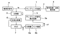
図9は、図7に示したサンプリング手法の原理で被測定信号aの信号波形dを測定する別の波形測定装置の概略構成を示す図である。
繰り返し周波数fa(繰り返し周期Ta)を有する被測定信号aはサンプリング回路1及び分周器5へ入力される。分周器5は、被測定信号aの繰り返し周波数faを1/nに分周して位相比較器6へ送出する。電圧制御発振器(VCO)7は、繰り返し周波数faの1/n(n;正整数)の周波数(fa/n)を有する信号を発生して位相比較器6へ帰還させる。
【0009】
位相比較器6は、電圧制御発振器(VCO)の出力信号の位相と分周器5の出力信号の位相との位相差を検出して位相差信号として電圧制御発振器(VCO)7へ送出する。このPLLループによって、電圧制御発振器(VCO)7からの出力信号の位相は被測定信号aの位相に同期する。
【0010】
電圧制御発振器(VCO)7から出力された周波数(fa/n)を有する出力信号の周波数(fa/n)は次の固定の分周器8aと固定の逓(てい)倍器8bとで[(fa/n)―Δf]の周波数に変換されて、サンプリング信号発生回路3aへ入力される。
【0011】
サンプリング信号発生回路3aは、入力された出力信号に同期する
繰り返し周波数fb=[(fa/n)―Δf] …(1)
繰り返し周期 Tb=[(nTa)+ΔT] …(2)
を有するサンプリング信号bをサンプリング回路1へ印加する。但し、ΔfとΔTとの関係は近似的に下式で示される。
【0012】
Δf/ΔT=fa2/n2 …(3)
サンプリング回路1は、入力された被測定信号aをサンプリング信号発生回路3aから入力されたサンプリング信号bでサンプリングして、サンプリングされた被測定信号cを信号処理・波形表示部4へ送出する。
【0013】
信号処理・波形表示部4は、入力されたサンプリングされた被測定信号cの包絡線波形を算出して、この包絡線波形の時間軸の目盛りを元の被測定信号aの目盛りに変換して、被測定信号aの信号波形dとして表示出力する。この場合、測定された包絡線波形の被測定信号aの信号波形dに対する拡大率は(fa/nΔf)である。
【0014】
なお、被測定信号aが電気信号でなくて、光信号の場合、この光信号を電気信号に変換して、タイマ回路2又は分周器5へ印加する。また、サンプリング回路1の代りに、電界吸収型光変調器を用いる。この電界吸収型光変調器は、入射された光信号の進行方向に対してサンプリング信号によるパルス状の電界を印加することによって、入力された光信号からなるパルス状の被測定信号aをサンプリングすることが可能である。そして、このサンプリングされた光信号からなる被測定信号cを電気信号に変換して信号処理・波形表示部4へ送出する。
【0015】
【発明が解決しようとする課題】
しかしながら、図8及び図9に示すサンプリング手法を用いた波形測定装置においてもまだ解消すべき次のような課題があった。
【0016】
すなわち、図8に示す波形測定装置においては、タイマ回路2が出力するタイミング信号の出力タイミングは、このタイマ回路2内に有する基準時間信号を用いて設定される。すなわち、発振器から出力される基準時間信号と、被測定信号aの繰り返し周期Taを決定する基準信号とは、ハード的に異なる信号発生器で作成された信号であるので、位相まで検証すると、全てのタイミングで常に一致していることはない。
【0017】
そのために、サンプリング回路1でサンプリングされた後の被測定信号cの包絡線波形に大きなジッタが発生し、被測定信号aの信号波形dの測定精度が低下する。例えば、被測定信号aの繰り返し周波数faが10GHz程度の場合、発生するジッタ量は数ps(ピコ・セカンド)に達し、受光器及び電気処理回路の帯域制限も考慮した最終の被測定信号aの信号波形dにおいて、波形の誤差範囲が10ps〜20psにも達する。
【0018】
また、図9に示す波形測定装置においては、サンプリング信号発生回路3aから出力される繰り返し周波数fb=[(fa/n)―Δf]を有するサンプリング信号bを作成するための逓(てい)倍器8bからの出力信号は、被測定信号aを分周する分周器5と、位相比較器6と電圧制御発振器(VCO)7とで構成されたPLL回路で作成される。
【0019】
すなわち、サンプリング信号bは測定対象の被測定信号aを加工して作成されるので、サンプリング信号bは被測定信号aに対して常に位相同期している。よって、図8の波形測定装置のように、サンプリング信号bを作成するための発振器を別途設けることはない。よって、ジッタの発生量が大幅に抑制される。
【0020】
しかしながら、サンプリング信号bの繰り返し周波数fbは、前述した(1)、(3)式からも明らかのように、被測定信号aの繰り返し周波数faの関数で示される。このことは、サンプリング信号bの繰り返し周波数fbを被測定信号aの繰り返し周波数faに対して独立して任意に設定できない。よって、被測定信号aの繰り返し周波数faが変化すると、測定された被測定信号aの信号波形dの時間分解能、すなわち測定精度が自動的に変化する。
【0021】
このことは、被測定信号aの信号波形dを任意の時間分解能で測定できないことを示す。また、各分周器5,8aの仕様特性等に起因してサンプリング信号bの繰り返し周波数fbの選択範囲も大きく制限される。
【0022】
本発明はこのような事情に鑑みてなされたものであり、サンプリング信号の周波数を得るための周波数信号を周波数信号発生器を用いて生成するとともに、この生成した周波数信号をPLL手法を用いて被測定信号に対して常時位相同期させることにより、被測定信号をサンプリングするサンプリング信号の周波数を被測定信号の繰り返し周波数に対して独立して任意に設定でき、ジッタ発生量を大幅に抑制した状態で、被測定信号の信号波形の測定精度を向上できるとともに、信号波形を任意の分解精度で測定できる波形測定装置を提供することを目的とする。
【0023】
【課題を解決するための手段】
本発明は、入力された任意の繰り返し周期を有する被測定信号を、この被測定信号の繰り返し周期より長い周期を有するサンプリング信号でサンプリングするサンプリング部と、このサンプリング部によってサンプリングされた被測定信号の包絡線波形を求め、この包絡線波形から被測定信号の信号波形を求めるデータ処理部とを有する波形測定装置に適用される。
【0024】
そして、上記課題を解消するために、本発明の請求項1の波形測定装置においては、基準信号入力端子(REF)を有し、該基準信号入力端子(REF)に印加される基準信号を用いて前記被測定信号の繰り返し周波数に等しい周波数を有する周波数信号を出力する周波数信号発生器(15)と、この周波数信号発生器(15)から出力された周波数信号の位相と前記被測定信号の位相との位相差を検出して位相差信号として出力する位相比較器(14)と、この位相比較器(14)から出力された位相差信号に基づいて前記被測定信号に位相同期した基準信号を発生して前記周波数信号発生器(15)の前記基準信号入力端子(REF)へ帰還させる電圧制御発振器(17)と、この電圧制御発振器(17)から出力される基準信号を用いて前記サンプリング信号を発生するサンプリング信号発生回路(18)とを備えている。
【0025】
このように構成された波形測定装置においては、サンプリング信号発生手段にて生成されるサンプリング信号は、電圧制御発振器から出力される基準信号に基づいて作成される。さらに、この基準信号の周波数は周波数信号発生器にて、被測定信号の繰り返し周波数に対して独立に任意の値に設定可能である。さらに、この基準信号の位相は、周波数信号発生器と位相比較器と電圧制御発振器とで構成されるPLL回路でもって、被測定信号の位相と常時位相同期が取れている状態である。
【0026】
よって、被測定信号をサンプリングするサンプリング信号の周波数を、被測定信号の繰り返し周波数に独立して任意に設定でき、かつ被測定信号に対して常時位相同期が取れているので、ジッタ発生が抑制される。
【0027】
請求項2においては、上記波形測定装置において、前記周波数信号発生器(15)から出力された周波数信号と前記被測定信号とをミキシングするミキサ回路(27)を備え、前記位相比較器(14)は、前記基準信号入力端子(REF)に印加される基準信号の位相と前記ミキサ回路(27)からの出力信号の位相との位相差を検出して位相差信号として出力するようにしている。
【0028】
請求項3においては、上記波形測定装置において、前記被測定信号の繰り返し周波数を1/n(n;正整数)に分周する分周器(28)を備え、前記周波数信号発生器(15)は、前記基準信号入力端子(REF)に印加される基準信号を用いて前記被測定信号の繰り返し周波数が1/n(n;正整数)に等しい周波数を有する周波数信号を出力し、前記位相比較器(14)は、前記周波数信号発生器(15)から出力された周波数信号の位相と前記分周器(28)によって繰り返し周波数を1/n(n;正整数)に分周された前記被測定信号の位相との位相差を検出して位相差信号として出力するようにしている。
【0029】
請求項4においては、上記波形測定装置において、前記基準信号の周波数のm(m;正整数)てい倍の周波数を有する信号を出力する周波数てい倍器(29)と、前記周波数信号発生器(15)から出力された周波数信号と前記被測定信号とをミキシングするミキサ回路(27)とを備え、前記周波数信号発生器(15)は、前記基準信号入力端子(REF)に印加される基準信号を用いて前記被測定信号の繰り返し周波数に等しい周波数と前記基準信号の周波数のm(m;正整数)てい倍の周波数とを加算または減算した周波数を有する周波数信号を出力し、前記位相比較器(14)は、前記基準信号入力端子(REF)に前記周波数てい倍器(29)から印加される前記基準信号の周波数のmてい倍の周波数を有する信号の位相と前記ミキサ回路(27)からの出力信号の位相との位相差を検出して位相差信号として出力する。
【0030】
請求項5においては、上記波形測定装置において、前記被測定信号の繰り返し周波数を測定する周波数測定部(26)と、この周波数測定部(26)で測定された被測定信号の繰り返し周波数に基づいて、前記周波数信号発生器(15)に対して該周波数信号発生器(15)から出力する周波数信号の周波数を設定する周波数設定部(16)とを備えている。
【0031】
請求項6においては、上記波形測定装置において、前記被測定信号が光信号であるとき、該光信号である前記被測定信号を2方向に分波する分波器(11)と、この分波器(11)で分波された一方の被測定信号からその繰り返し周期のクロックを検出することにより、前記光信号である被測定信号を、前記繰り返し周波数を有する正弦波波形の電気信号の被測定信号に変換して出力するクロック再生器(13)とを備えている。
請求項7においては、上記波形測定装置において、前記サンプリング部(12)が電界吸収型変調器(12)であるとき、該電界吸収型変調器(12)によって、前記分波器(11)から入力された、光信号の被測定信号を前記サンプリング信号発生回路(18)から入力されたサンプリング信号でサンプリングして得られた光信号の被測定信号を受光してサンプリング後の光信号である被測定信号を電気信号の被測定信号に変換する受光器(21)と、前記受光器(21)によって電気信号に変換された被測定信号をデジタルの被測定信号に変換して、前記データ処理部(23)へ送出するアナログ/デジタル変換器(22)と、前記データ処理部(23)によって求められた前記包絡線波形の時間軸の目盛りを元の被測定信号の目盛りに変換して、前記被測定信号の信号波形として表示する表示器(24)とを備えている。
【0032】
【発明の実施の形態】
以下、本発明の各実施形態を図面を用いて説明する。
(第1実施形態)
図1は本発明の第1実施形態に係わる波形測定装置の概略構成を示すブロック図である。
【0033】
入力端子から入力された、例えば図7に示す繰り返し周期Ta(繰り返し周波数fa)を有する光信号からなる被測定信号aは分波器11で2方向に分波されて、一方はサンプリング回路としての電界吸収型変調器12へ入射され、他方はクロック再生器13へ入射される。なお、この実施形態装置においては、被測定信号aの繰り返し周波数faは10GHzに設定されている。
【0034】
クロック再生器13は、入射された光信号からなる被測定信号aにおける繰り返し周期Taの開始タイミング、すなわち、繰り返し周期Taのクロックを検出して、入射された光信号からなる被測定信号aを、周波数fa(繰り返し周波数)を有する正弦波波形の電気信号の被測定信号a1に変換して次の位相比較器14へ送出する。
【0035】
周波数信号発生器15は、例えばシンセサイザ等で形成されており、基準信号入力端子に印加されている基準信号eを逓倍又は分周することによって、任意の周波数を有した周波数信号gを作成可能である。具体的には、電圧制御発振器(VCO)17から印加されている10MHzの基準信号eを用いて、コンピュータからなる制御部16から指示された被測定信号aの繰り返し周波数である10GHzの周波数faを有する周波数信号gを作成して出力する。この場合、基準信号eを1000倍に逓倍している。そして、当然、出力される周波数信号gの位相は基準信号eの位相に1対1で完全に同期している。
【0036】
周波数信号発生器15から出力された周波数faを有する周波数信号gは位相比較器14へ印加される。位相比較器14は、クロック再生器13から入力された電気信号に変換された周波数faを有する被測定信号a1の位相と周波数faを有する周波数信号gの位相との位相差を検出して位相差信号hとして、電圧制御発振器(VCO)17へ送出する。
【0037】
電圧制御発振器(VCO)17は、前述した10MHzの基準信号eを発生して周波数信号発生器15の基準信号入力端子へ印加する。位相比較器14と電圧制御発振器(VCO)17と周波数信号発生器15とはPLL回路を構成するので、電圧制御発振器(VCO)17から出力される基準信号eの位相は、常時、被測定信号a1の位相に同期している。
【0038】
電圧制御発振器(VCO)17から出力される基準信号eは周波数信号発生器15に帰還されると共に、サンプリング信号bを発生するサンプリング信号発生回路18へ入力される。サンプリング信号発生回路18は、信号発生器19と波形整形回路20とで構成されている。
【0039】
信号発生器19は、前出した周波数信号発生器15と同様に、例えばシンセサイザ等で形成されており、基準信号入力端子に印加されている基準信号eを逓倍又は分周することによって、任意の周波数を有した信号を作成可能である。具体的には、電圧制御発振器(VCO)17から印加されている10MHzの基準信号eを用いて、制御部16から指示されたサンプリング信号bの周波数fbである999.9MHzの周波数を有する信号を作成して出力する。
【0040】
ここで、サンプリング信号bの周波数fbと被測定信号aの繰り返し周波数faとの関係を検証すると、前述した(1)式に、fa=10GHz、fb=999.9MHzを代入すると、
fb=(fa/n)―Δf …(1)
例えば、n=10、Δf=0.1MHzで(1)式が成立する。
【0041】
信号発生器19から出力された正弦波形の信号は、次の波形整形回路20で、図7に示すような繰り返し周波数fb(繰り返し周期Tb)を有するパルス波形状のサンプリング信号bに波形整形される。サンプリング信号発生回路18から出力された周波数fbを有するサンプリング信号bは電界吸収型変調器12へ入力される。
【0042】
電界吸収型変調器12は、前述したように、入力された光信号の被測定信号aをサンプリング信号発生回路18から入力されたサンプリング信号bでサンプリングして、サンプリングされた光信号の被測定信号cを受光器21へ送出する。
【0043】
受光器21は、入射されたサンプリング後の光信号の被測定信号cを電気信号の被測定信号c1に変換する。受光器21から出力された被測定信号c1はA/D器22でデジタルのサンプリングされた被測定信号c2 にA/D変換されて、データ処理部23へ入力される。
【0044】
データ処理部23は、入力されたサンプリングされた被測定信号c1の包絡線波形を算出して、この包絡線波形の時間軸の目盛りを元の被測定信号aの目盛りに変換して、被測定信号aの信号波形dとして表示器24に表示出力する。
【0045】
このように構成された第1実施形態の波形測定装置においては、この波形測定装置の操作者は制御部16を介して、サンプリング信号発生回路18の信号発生器19に対して、被測定信号aの繰り返し周波数faに対して、全く独立して、サンプリング信号bの繰り返し周波数fbを設定可能である。
【0046】
この場合、サンプリング信号発生回路18の信号発生器19に印加される基準信号eの位相は、位相比較器14と電圧制御発振器(VCO)17と周波数信号発生器15とで構成されるPLL回路の位相制御機能により、被測定信号aの位相と常時完全に一致している。
【0047】
したがって、被測定信号をサンプリングするサンプリング信号bの周波数fbを、被測定信号aの繰り返し周波数faに独立して任意に設定でき、かつサンプリング信号bは被測定信号aに対して常時位相同期が取れているので、ジッタ発生量が抑制される。
よって、ジッタ発生量を大幅に抑制した状態で、被測定信号aの信号波形dの測定精度を向上できるとともに、信号波形dを任意の分解精度で測定できる。
【0048】
(第2実施形態)
図2は本発明の第2実施形態に係わる波形測定装置の概略構成を示すブロック図である。図1に示した第1実施形態の波形測定装置と同一部には同一符号を付して、重複する部分の詳細説明を省略する。
【0049】
この第2実施形態の波形測定装置においては、クロック再生器13から出力された電気信号の被測定信号a1は位相比較器14へ入力されると共に分波器25で分波されて、周波数カウンタ26へ入力される。周波数カウンタ26は、入力された電気信号の被測定信号a1の繰り返し周波数faを測定して、測定された繰り返し周波数faのデータを制御部16へ送出する。なお、周波数カウンタ26には、被測定信号a1のクロック(波形)のタイミングとクロックカウントのタイミングの同期を取るために、電圧制御発振器17から基準信号eが入力されている。
【0050】
制御部16は、周波数カウンタ26から入力された被測定信号aの繰り返し周波数faを周波数信号発生器15に対して、出力される周波数信号gの周波数として設定する。したがって、周波数信号発生器15は、図1に示す第1実施形態の波形測定装置における周波数信号発生器15と同様に、被測定信号aの繰り返し周波数と同一の周波数faを有する周波数信号gを次の位相比較器14へ送出する。これ以降の動作は、図1に示した第1実施形態の波形測定装置の動作と同じである。
【0051】
このように構成された第2実施形態の波形測定装置においては、周波数カウンタ26で、被測定信号aの繰り返し周波数faを測定して、周波数信号発生器15に設定しているので、第1実施形態の波形測定装置と同様に、ジッタの発生量を抑制した状態で、被測定信号aの信号波形dを任意の分解精度で測定できる。
【0052】
さらに、この第2実施形態の波形測定装置においては、たとえ被測定信号aの繰り返し周波数faが不明であったとしても、被測定信号aの信号波形dを正しく測定できる。
【0053】
(第3実施形態)
図3は本発明の第3実施形態に係わる波形測定装置の概略構成を示すブロック図である。図1に示した第1実施形態の波形測定装置と同一部には同一符号を付して、重複する部分の詳細説明を省略する。
【0054】
この第3実施形態の波形測定装置においては、周波数信号発生器15と位相比較器14との間にミキサ回路27が介挿されている。そして、クロック再生器13から出力された電気信号の被測定信号a1は、位相比較器14へ入力されずに、ミキサ回路27へ入力される。電圧制御発振器(VCO)17は、10MHzの周波数を有した基準信号eを周波数信号発生器15の基準信号入力端子へ印加すると共に、位相比較器14の他方の入力端へ印加される。さらに、周波数信号発生器15には、制御部16から被測定信号aの繰り返し周波数faに基準信号の周波数を加算した周波数が設定周波数として入力される。
【0055】
このような構成の第3実施形態の波形測定装置において、周波数信号発生器15は、被測定信号aの繰り返し周波数faに基準信号の周波数を加算した周波数を有する周波数信号gを出力する。この実施形態装置においては、被測定信号aの繰り返し周波数faが10GHzであり、基準信号eの周波数が10MHzであるので、(10GHz+10MHz)の周波数を有した周波数信号gが次のミキサ回路27へ送出される。
【0056】
ミキサ回路27は周波数信号発生器15から出力された周波数信号gとクロック再生器13から出力された被測定信号a1とを信号合成する。したがって、ミキサ回路27の出力信号jは、周波数信号gの周波数(10GHz+10MHz)と被測定信号a1の周波数(10GHz)との差の周波数(10MHz)の成分を有する。ミキサ回路27の出力信号jは位相比較器14へ送出される。したがって、この出力信号jには、被測定信号a1と周波数信号g内の基準信号eとの位相差成分が含まれる。
【0057】
位相比較器14は、ミキサ回路27の出力信号jの位相と基準信号eの位相との位相差を検出して位相差信号hとして、電圧制御発振器(VCO)17へ印加する。電圧制御発振器(VCO)17は、前述した10MHzの基準信号eを発生して周波数信号発生器15の基準信号入力端子と位相比較器14へ印加する。ミキサ回路27と位相比較器14と電圧制御発振器(VCO)17と周波数信号発生器15とはPLL回路を構成するので、電圧制御発振器(VCO)17から出力される基準信号eの位相は、常時、被測定信号a1の位相に同期している。
【0058】
電圧制御発振器(VCO)17から出力される10MHzの基準信号eは周波数信号発生器15に帰還されると共に、サンプリング信号発生貌路18へ入力される。サンプリング信号発生貌路18は、図7に示すサンプリング信号bを発生して電界吸収型変調器12へ印加する。
【0059】
したがって、この第3実施形態の波形測定装置においても、入力された被測定信号aの信号波形dを測定できる。
さらに、この第3実施形態の波形測定装置においては、ミキサ回路27を周波数信号発生器15と位相比較器14との間に介挿することによって、位相比較器14へ入力されるミキサ回路27の出力信号jの周波数成分を基準信号eの周波数成分に低下できるので、高速処理可能な位相比較器14を採用する必要はない。したがって、波形測定装置の製造費を低下できると共に、測定された信号波形dの測定精度を向上できる。
【0060】
(第4実施形態)
図4は本発明の第4実施形態に係わる波形測定装置の概略構成を示すブロック図である。図2に示した第2実施形態の波形測定装置及び図3に示した第3実施形態の波形測定装置と同一部には同一符号を付して、重複する部分の詳細説明を省略する。
【0061】
この第4実施形態の波形測定装置においては、図3に示した第3実施形態の波形測定装置に対して、図2に示した第2実施形態の波形測定装置における分波器25及び周波数カウンタ26を付加している。
【0062】
すなわち、クロック再生器13から出力された被測定信号a1はミキサ回路27へ入力されると共に分波器25で分波されて、周波数カウンタ26へ入力される。周波数カウンタ26は、入力された電気信号の被測定信号a1の繰り返し周波数faを測定して、測定された繰り返し周波数faのデータを制御部16へ送出する。
【0063】
制御部16は、周波数カウンター26から入力された被測定信号aの繰り返し周波数faに基準信号eの周波数を加算した周波数を波数信号発生器15に対して設定する。したがって、周波数信号発生器15は、図3に示す第3実施形態の波形測定装置における周波数信号発生器15と同様に、被測定信号aの繰り返し周波数faに基準信号の周波数を加算した周波数を有する周波数信号gを出力する。
【0064】
よつて、第3実施形態装置と同様に、入力された被測定信号aの信号波形dを測定できる。
さらに、この第4実施形態の波形測定装置においては、たとえ被測定信号aの繰り返し周波数faが不明であったとしても、被測定信号aの信号波形dを正しく測地できる。
【0065】
(第5実施形態)
図5は本発明の第5実施形態に係わる波形測定装置の概略構成を示すブロック図である。図1に示した第1実施形態の波形測定装置と同一部には同一符号を付して、重複する部分の詳細説明を省略する。
【0066】
この実施形態装置においては、クロック再生器13と位相比較器14との間に分周器28が介挿されている。この分周器28は、クロック再生器13から出力される周波数faを有する電気信号a1を周波数信号発生器15から出力される周波数信号gの周波数に一致させる機能を有する。
【0067】
このように、クロック再生器13と位相比較器14との間に分周器28を設けることによって、周波数信号発生器15から出力される周波数信号gの周波数を必ずしも被測定信号aの周波数周faに一致させる必要はない。図5の実施形態装置においては、被測定信号aの周波数周faが40GHzで、周波数信号発生器15の周波数信号gの周波数が1/4(n=4)の10GHzであるので、分周器28の分周比は4に設定されている。
【0068】
(第6実施形態)
図6は本発明の第6実施形態に係わる波形測定装置の概略構成を示すブロック図である。図3に示した第3実施形態の波形測定装置と同一部には同一符号を付して、重複する部分の詳細説明を省略する。
【0069】
この実施形態装置においては、電圧制御発振器17と位相比較器14との間に逓(てい)倍器29が介挿されている。この逓(てい)倍器29は電圧制御発振器17から出力される10MHzの基準信号eの周波数をN倍(m=N)に逓(てい)倍して、位相比較器14へ印加される基準信号eの周波数をミキサ回路27から位相比較器14へ出力される出力信号jの周波数に一致させる機能を有する。
【0070】
したがって、制御部16から周波数信号発生器15へ設定する周波数は(10GHz+10MHz)でなくて、[10GHz+(N×10)MHz]となり、設定の自由度が上昇する。
【0071】
なお、本発明は上述した各実施形態に限定されるものではない。各実施形態装置においては、被測定信号aは光信号であると仮定した。しかし、被測定信号aは通常の電気信号であってもよい。
【0072】
この場合、電界吸収型変調器12への電気入力信号を被測定信号とし、光入力信号をサンプリング信号とすることにより、電気信号のサンプリングも可能である。このとき、サンプリング信号発生回路18は短パルス光源などを用いた光信号を出力する信号発生回路となる。また、電界吸収型変調器12の代りに、図7、図9に示す通常の電気信号に適用されるサンプリング回路1を採用することもできる。
【0073】
【発明の効果】
以上説明したように、本発明の波形測定装置においては、サンプリング信号の繰り返し周波数を得るための周波数信号を周波数信号発生器を用いて生成するとともに、この生成した周波数信号をPLL手法を用いて被測定信号に対して常時位相同期するようにしている。
【0074】
したがって、被測定信号をサンプリングするサンプリング信号の周波数を任意に設定でき、ジッタ発生量を大幅に抑制した状態で、被測定信号の信号波形の測定精度を向上できるともに、信号波形を任意の分解精度で測定できる。
【図面の簡単な説明】
【図1】本発明の第1実施形態に係わる波形測定装置の概略構成を示すブロック図
【図2】本発明の第2実施形態に係わる波形測定装置の概略構成を示すブロック図
【図3】本発明の第3実施形態に係わる波形測定装置の概略構成を示すブロック図
【図4】本発明の第4実施形態に係わる波形測定装置の概略構成を示すブロック図
【図5】本発明の第5実施形態に係わる波形測定装置の概略構成を示すブロック図
【図6】 本発明の第6実施形態に係わる波形測定装置の概略構成を示すブロック図
【図7】被測定信号の信号波形をサンプリング手法を用いて求める原理を説明するための図
【図8】従来の波形測定装置の概略構成を示すブロック図
【図9】別の従来の波形測定装置の概略構成を示すブロック図
【符号の説明】
a…被測定信号
b…サンプリング信号
d…信号波形
e…基準信号
g…周波数信号
h…位相差信号
11,25…分波器
12…電界吸収型変調器
13…クロック再生器
14…位相比較器
15…周波数信号発生器
16…制御部
17…電圧制御発振器
18…サンプリング信号発生回路
19…信号発生器
20…波形整形回路
21…受光器
23…データ処理部
24…表示器
26…周波数カウンタ
27…ミキサ回路[0001]
BACKGROUND OF THE INVENTION
The present invention relates to a waveform measuring apparatus for obtaining a signal waveform of a signal under measurement having an arbitrary repetition period inputted.Related.
[0002]
[Prior art]
Various measurement techniques have been proposed for measuring the signal waveform of a signal under measurement including an input electric signal or optical signal having an arbitrary repetition period. However, in the case of a high frequency signal with a repetition period of the signal under measurement, that is, a repetition frequency exceeding 10 GHz, the signal waveform of the signal under measurement cannot be observed directly on a display screen such as an oscilloscope, so the selection range of the waveform measurement method is naturally limited. There is.
[0003]
A typical method for measuring the signal waveform of the signal under measurement whose repetition frequency exceeds 10 GHz will be described with reference to FIG. A signal under measurement a having a repetition period Ta (for example, repetition frequency fa = 10 GHz) is sampled with a sampling signal b having a period Tb (for example, repetition frequency fb = 999.9 MHz) longer than the repetition period Ta of the signal under measurement a. To do. In this case, the relationship between the repetition periods Ta and Tb is adjusted, and as shown in FIG. 7, the sampling position of the sampling signal b in the signal waveform within the repetition period Ta of the signal under measurement a is very small as time passes. Shift by ΔT.
[0004]
Therefore, the signal under measurement c after being sampled by the sampling signal b becomes a discrete waveform in which a pulsed waveform appears at a position synchronized with the sampling signal b, as shown in the figure. And the envelope waveform of each pulse-like waveform isMeasured signal aThe signal waveform d is enlarged in the time axis direction.
[0005]
A waveform measuring apparatus for measuring the signal waveform d of the signal under measurement a based on the principle of the sampling method shown in FIG. 7 is configured as shown in FIG. 8, for example.
A signal under measurement a having a repetition period Ta (repetition frequency fa) is input to the
[0006]
The sampling
[0007]
The signal processing /
[0008]
FIG. 9 is a diagram showing a schematic configuration of another waveform measuring apparatus that measures the signal waveform d of the signal under measurement a based on the principle of the sampling method shown in FIG.
A signal under measurement a having a repetition frequency fa (repetition period Ta) is input to the
[0009]
The
[0010]
The frequency (fa / n) of the output signal having the frequency (fa / n) output from the voltage controlled oscillator (VCO) 7 is determined by the following
[0011]
The sampling
Repetition frequency fb = [(fa / n) −Δf] (1)
Repetition period Tb = [(nTa) + ΔT] (2)
Is applied to the
[0012]
Δf / ΔT = fa2/ N2 … (3)
The
[0013]
The signal processing /
[0014]
When the signal to be measured a is not an electrical signal but an optical signal, the optical signal is converted into an electrical signal and applied to the
[0015]
[Problems to be solved by the invention]
However, the waveform measuring apparatus using the sampling method shown in FIGS. 8 and 9 still has the following problems to be solved.
[0016]
That is, in the waveform measuring apparatus shown in FIG. 8, the output timing of the timing signal output from the
[0017]
Therefore, a large jitter occurs in the envelope waveform of the signal under measurement c after being sampled by the
[0018]
In the waveform measuring apparatus shown in FIG. 9, a multiplier for creating a sampling signal b having a repetition frequency fb = [(fa / n) −Δf] output from the sampling
[0019]
That is, since the sampling signal b is created by processing the signal under measurement a to be measured, the sampling signal b is always in phase synchronization with the signal under measurement a. Therefore, unlike the waveform measuring apparatus of FIG. 8, there is no need to separately provide an oscillator for creating the sampling signal b. Therefore, the amount of jitter generated is greatly suppressed.
[0020]
However, the repetition frequency fb of the sampling signal b is expressed as a function of the repetition frequency fa of the signal under measurement a, as is clear from the above-described equations (1) and (3). This means that the repetition frequency fb of the sampling signal b cannot be arbitrarily set independently of the repetition frequency fa of the signal under measurement a. Therefore, when the repetition frequency fa of the signal under measurement a changes, the time resolution of the measured signal waveform d of the signal under measurement a, that is, the measurement accuracy automatically changes.
[0021]
This indicates that the signal waveform d of the signal under measurement a cannot be measured with an arbitrary time resolution. Each
[0022]
The present invention has been made in view of such circumstances. A frequency signal for obtaining the frequency of a sampling signal is generated using a frequency signal generator, and the generated frequency signal is subjected to a PLL method. By always synchronizing the phase with the measurement signal, the frequency of the sampling signal for sampling the signal under measurement can be set arbitrarily and independently with respect to the repetition frequency of the signal under measurement, while greatly reducing the amount of jitter generated. An object of the present invention is to provide a waveform measuring apparatus that can improve the measurement accuracy of the signal waveform of the signal under measurement and can measure the signal waveform with an arbitrary resolution accuracy.
[0023]
[Means for Solving the Problems]
The present invention samples an input signal under measurement having an arbitrary repetition period with a sampling signal having a period longer than the repetition period of the signal under measurement.Sampling unit and this sampling unitObtain the envelope waveform of the sampled signal under measurement, and obtain the signal waveform of the signal under measurement from this envelope waveformData processing unitApplied to waveform measuring equipment.
[0024]
And in order to eliminate the said subject, in the waveform measuring device of
[0025]
In the waveform measuring apparatus configured as described above, the sampling signal generated by the sampling signal generating means is generated based on the reference signal output from the voltage controlled oscillator. Further, the frequency of the reference signal can be set to an arbitrary value independently of the repetition frequency of the signal under measurement by the frequency signal generator. Further, the phase of the reference signal is always in phase synchronization with the phase of the signal under measurement by a PLL circuit including a frequency signal generator, a phase comparator, and a voltage controlled oscillator.
[0026]
Therefore, the frequency of the sampling signal for sampling the signal under measurement can be arbitrarily set independently of the repetition frequency of the signal under measurement, and the phase synchronization with the signal under measurement is always taken, so jitter generation is suppressed. The
[0027]
The waveform measurement apparatus according to
[0028]
The waveform measuring apparatus according to
[0029]
According to a fourth aspect of the present invention, in the waveform measuring apparatus, a frequency multiplier that outputs a signal having a frequency that is m (m; a positive integer) double the frequency of the reference signal.29) And a mixer circuit (27) for mixing the frequency signal output from the frequency signal generator (15) and the signal under measurement, and the frequency signal generator (15) includes the reference signal input terminal. A frequency having a frequency obtained by adding or subtracting a frequency equal to the repetition frequency of the signal under measurement and a frequency m (m; a positive integer) times the frequency of the reference signal using a reference signal applied to (REF). The phase comparator (14) outputs a signal having a frequency m times the frequency of the reference signal applied from the frequency multiplier (29) to the reference signal input terminal (REF). A phase difference between the phase and the phase of the output signal from the mixer circuit (27) is detected and output as a phase difference signal.
[0030]
According to
[0031]
According to a sixth aspect of the present invention, in the waveform measuring apparatus, when the signal under measurement is an optical signal, a demultiplexer (11) for demultiplexing the signal under measurement as the optical signal in two directions, By detecting a clock having a repetition period from one of the signals under measurement demultiplexed by the device (11), the signal under measurement, which is the optical signal, is measured as an electric signal having a sinusoidal waveform having the repetition frequency. Clock regenerator that converts to a signal and outputs it (13).
In the waveform measurement device according to
[0032]
DETAILED DESCRIPTION OF THE INVENTION
Hereinafter, embodiments of the present invention will be described with reference to the drawings.
(First embodiment)
FIG. 1 is a block diagram showing a schematic configuration of a waveform measuring apparatus according to the first embodiment of the present invention.
[0033]
For example, a signal under measurement a input from an input terminal and made up of an optical signal having a repetition period Ta (repetition frequency fa) shown in FIG. The light is incident on the
[0034]
The
[0035]
The
[0036]
The frequency signal g having the frequency fa output from the
[0037]
The voltage controlled oscillator (VCO) 17 generates the above-described 10 MHz reference signal e and applies it to the reference signal input terminal of the
[0038]
The reference signal e output from the voltage controlled oscillator (VCO) 17 is fed back to the
[0039]
The
[0040]
Here, when the relationship between the frequency fb of the sampling signal b and the repetition frequency fa of the signal under measurement a is verified, if fa = 10 GHz and fb = 999.9 MHz are substituted into the above-described equation (1),
fb = (fa / n) −Δf (1)
For example, equation (1) is established when n = 10 and Δf = 0.1 MHz.
[0041]
The sine waveform signal output from the
[0042]
As described above, the
[0043]
The
[0044]
The
[0045]
In the waveform measuring apparatus of the first embodiment configured as described above, an operator of this waveform measuring apparatus sends a signal to be measured a to the
[0046]
In this case, the phase of the reference signal e applied to the
[0047]
Therefore, the frequency fb of the sampling signal b for sampling the signal under measurement can be arbitrarily set independently of the repetition frequency fa of the signal under measurement a, and the sampling signal b is always in phase synchronization with the signal under measurement a. Therefore, the amount of jitter generated is suppressed.
Therefore, the measurement accuracy of the signal waveform d of the signal to be measured a can be improved and the signal waveform d can be measured with an arbitrary resolution accuracy in a state where the amount of jitter generation is greatly suppressed.
[0048]
(Second Embodiment)
FIG. 2 is a block diagram showing a schematic configuration of a waveform measuring apparatus according to the second embodiment of the present invention. The same parts as those of the waveform measuring apparatus of the first embodiment shown in FIG. 1 are denoted by the same reference numerals, and detailed description of the overlapping parts is omitted.
[0049]
In the waveform measuring apparatus of the second embodiment, the signal under measurement a of the electrical signal output from the
[0050]
The
[0051]
In the waveform measuring apparatus of the second embodiment configured as described above, the frequency counter 26 measures the repetition frequency fa of the signal to be measured a and sets it in the
[0052]
Furthermore, in the waveform measuring apparatus of the second embodiment, even if the repetition frequency fa of the signal under measurement a is unknown, the signal waveform d of the signal under measurement a is correctly set.Measurementit can.
[0053]
(Third embodiment)
FIG. 3 is a block diagram showing a schematic configuration of a waveform measuring apparatus according to the third embodiment of the present invention. The same parts as those of the waveform measuring apparatus of the first embodiment shown in FIG. 1 are denoted by the same reference numerals, and detailed description of the overlapping parts is omitted.
[0054]
In the waveform measuring apparatus of the third embodiment, a
[0055]
In the waveform measuring apparatus of the third embodiment having such a configuration, the
[0056]
The
[0057]
The
[0058]
The reference signal e of 10 MHz output from the voltage controlled oscillator (VCO) 17 is fed back to the
[0059]
Therefore, the waveform measuring apparatus of the third embodiment can also measure the signal waveform d of the input signal under measurement a.
Further, in the waveform measuring apparatus of the third embodiment, the
[0060]
(Fourth embodiment)
FIG. 4 is a block diagram showing a schematic configuration of a waveform measuring apparatus according to the fourth embodiment of the present invention. The same parts as those of the waveform measuring apparatus of the second embodiment shown in FIG. 2 and the waveform measuring apparatus of the third embodiment shown in FIG. 3 are denoted by the same reference numerals, and detailed description of the overlapping parts is omitted.
[0061]
In the waveform measuring apparatus of the fourth embodiment, the
[0062]
That is, the signal under measurement a output from the
[0063]
The
[0064]
Therefore, the signal waveform d of the input signal to be measured a can be measured as in the third embodiment.
Furthermore, in the waveform measuring apparatus of the fourth embodiment, the signal waveform d of the signal under measurement a can be correctly measured even if the repetition frequency fa of the signal under measurement a is unknown.
[0065]
(Fifth embodiment)
FIG. 5 is a block diagram showing a schematic configuration of a waveform measuring apparatus according to the fifth embodiment of the present invention. The same parts as those of the waveform measuring apparatus of the first embodiment shown in FIG. 1 are denoted by the same reference numerals, and detailed description of the overlapping parts is omitted.
[0066]
In this embodiment, a
[0067]
Thus, by providing the
[0068]
(Sixth embodiment)
FIG. 6 is a block diagram showing a schematic configuration of a waveform measuring apparatus according to the sixth embodiment of the present invention. The same parts as those of the waveform measuring apparatus of the third embodiment shown in FIG. 3 are denoted by the same reference numerals, and detailed description of the overlapping parts is omitted.
[0069]
In this embodiment apparatus, a
[0070]
Therefore, the frequency set from the
[0071]
In addition, this invention is not limited to each embodiment mentioned above. In each of the embodiments, the signal under measurement a is assumed to be an optical signal. However, the signal under measurement a may be a normal electric signal.
[0072]
In this case, the electrical signal can be sampled by using the electrical input signal to the
[0073]
【The invention's effect】
As described above, in the waveform measuring apparatus of the present invention, the frequency signal for obtaining the repetition frequency of the sampling signal is generated using the frequency signal generator, and the generated frequency signal is processed using the PLL technique. The phase is always synchronized with the measurement signal.
[0074]
Therefore, it is possible to arbitrarily set the frequency of the sampling signal for sampling the signal under measurement, while improving the measurement accuracy of the signal waveform of the signal under measurement while greatly reducing the amount of jitter generation, the signal waveform can be arbitrarily resolved. Can be measured.
[Brief description of the drawings]
FIG. 1 is a block diagram showing a schematic configuration of a waveform measuring apparatus according to a first embodiment of the present invention.
FIG. 2 is a block diagram showing a schematic configuration of a waveform measuring apparatus according to a second embodiment of the present invention.
FIG. 3 is a block diagram showing a schematic configuration of a waveform measuring apparatus according to a third embodiment of the present invention.
FIG. 4 is a block diagram showing a schematic configuration of a waveform measuring apparatus according to a fourth embodiment of the present invention.
FIG. 5 is a block diagram showing a schematic configuration of a waveform measuring apparatus according to a fifth embodiment of the present invention.
FIG. 6 of the present invention6thThe block diagram which shows schematic structure of the waveform measuring apparatus concerning embodiment
FIG. 7 is a diagram for explaining the principle of obtaining a signal waveform of a signal under measurement using a sampling method;
FIG. 8 is a block diagram showing a schematic configuration of a conventional waveform measuring apparatus.
FIG. 9 is a block diagram showing a schematic configuration of another conventional waveform measuring apparatus.
[Explanation of symbols]
a: Signal to be measured
b ... Sampling signal
d: Signal waveform
e ... Reference signal
g ... Frequency signal
h: Phase difference signal
11, 25 ... branching filter
12 ... Electroabsorption modulator
13 ... Clock regenerator
14 ... Phase comparator
15 ... Frequency signal generator
16 ... Control unit
17 ... Voltage controlled oscillator
18 ... Sampling signal generation circuit
19 ... Signal generator
20 ... Waveform shaping circuit
21 ... Receiver
23: Data processing unit
24 ... Display
26 ... Frequency counter
27. Mixer circuit
Claims (7)
基準信号入力端子(REF)を有し、該基準信号入力端子(REF)に印加される基準信号を用いて前記被測定信号の繰り返し周波数に等しい周波数を有する周波数信号を出力する周波数信号発生器(15)と、
この周波数信号発生器(15)から出力された周波数信号の位相と前記被測定信号の位相との位相差を検出して位相差信号として出力する位相比較器(14)と、
この位相比較器(14)から出力された位相差信号に基づいて前記被測定信号に位相同期した基準信号を発生して前記周波数信号発生器(15)の前記基準信号入力端子(REF)へ帰還させる電圧制御発振器(17)と、
この電圧制御発振器(17)から出力される基準信号を用いて前記サンプリング信号を発生するサンプリング信号発生回路(18)と
を備えたことを特徴とする波形測定装置。A sampling section (12) for sampling the input signal under measurement having an arbitrary repetition period with a sampling signal having a period longer than the repetition period of the signal under measurement, and the measurement target sampled by the sampling section (12) In a waveform measuring apparatus having a data processing unit (23) for obtaining an envelope waveform of a signal and obtaining a signal waveform of the signal under measurement from the envelope waveform,
A frequency signal generator having a reference signal input terminal (REF) and outputting a frequency signal having a frequency equal to the repetition frequency of the signal under measurement using the reference signal applied to the reference signal input terminal (REF). 15)
A phase comparator (14) for detecting a phase difference between the phase of the frequency signal output from the frequency signal generator (15) and the phase of the signal under measurement and outputting it as a phase difference signal;
Based on the phase difference signal output from the phase comparator (14), a reference signal synchronized with the signal under measurement is generated and fed back to the reference signal input terminal (REF) of the frequency signal generator (15). A voltage controlled oscillator (17)
A waveform measuring apparatus comprising: a sampling signal generating circuit (18) for generating the sampling signal using a reference signal output from the voltage controlled oscillator (17).
前記位相比較器(14)は、前記基準信号入力端子(REF)に印加される基準信号の位相と前記ミキサ回路(27)からの出力信号の位相との位相差を検出して位相差信号として出力する
ことを特徴とする請求項1記載の波形測定装置。A mixer circuit (27) for mixing the frequency signal output from the frequency signal generator (15) and the signal under measurement;
The phase comparator (14) detects the phase difference between the phase of the reference signal applied to the reference signal input terminal (REF) and the phase of the output signal from the mixer circuit (27), and uses it as a phase difference signal. The waveform measuring apparatus according to claim 1, wherein the waveform measuring apparatus outputs the waveform.
前記周波数信号発生器(15)は、前記基準信号入力端子(REF)に印加される基準信号を用いて前記被測定信号の繰り返し周波数が1/n(n;正整数)に等しい周波数を有する周波数信号を出力し、
前記位相比較器(14)は、前記周波数信号発生器(15)から出力された周波数信号の位相と前記分周器(28)によって繰り返し周波数を1/n(n;正整数)に分周された前記被測定信号の位相との位相差を検出して位相差信号として出力する
ことを特徴とする請求項1記載の波形測定装置。A frequency divider (28) that divides the repetition frequency of the signal under measurement into 1 / n (n; positive integer);
The frequency signal generator (15) has a frequency having a repetition frequency of the signal under measurement equal to 1 / n (n: positive integer) using a reference signal applied to the reference signal input terminal (REF). Output signal,
The phase comparator (14) divides the frequency of the frequency signal output from the frequency signal generator (15) by 1 / n (n: positive integer) by the frequency divider and the frequency divider (28). 2. The waveform measuring apparatus according to claim 1, wherein a phase difference from the phase of the signal under measurement is detected and output as a phase difference signal.
前記周波数信号発生器(15)から出力された周波数信号と前記被測定信号とをミキシングするミキサ回路(27)とを備え、
前記周波数信号発生器(15)は、前記基準信号入力端子(REF)に印加される基準信号を用いて前記被測定信号の繰り返し周波数に等しい周波数と前記基準信号の周波数のm(m;正整数)てい倍の周波数とを加算または減算した周波数を有する周波数信号を出力し、
前記位相比較器(14)は、前記基準信号入力端子(REF)に前記周波数てい倍器(29)から印加される前記基準信号の周波数のmてい倍の周波数を有する信号の位相と前記ミキサ回路(27)からの出力信号の位相との位相差を検出して位相差信号として出力する
ことを特徴とする請求項1記載の波形測定装置。A frequency multiplier ( 29 ) for outputting a signal having a frequency that is m (m; a positive integer) times the frequency of the reference signal;
A mixer circuit (27) for mixing the frequency signal output from the frequency signal generator (15) and the signal under measurement;
The frequency signal generator (15) uses a reference signal applied to the reference signal input terminal (REF), and a frequency equal to the repetition frequency of the signal under measurement and m (m; positive integer) of the frequency of the reference signal ) Outputs a frequency signal having a frequency obtained by adding or subtracting twice the frequency,
The phase comparator (14) includes a phase of a signal having a frequency that is m times the frequency of the reference signal applied from the frequency multiplier (29) to the reference signal input terminal (REF), and the mixer circuit. The waveform measuring apparatus according to claim 1, wherein a phase difference from the phase of the output signal from (27) is detected and output as a phase difference signal.
この周波数測定部(26)で測定された被測定信号の繰り返し周波数に基づいて、前記周波数信号発生器(15)に対して該周波数信号発生器(15)から出力する周波数信号の周波数を設定する周波数設定部(16)と
を備えたことを特徴とする請求項1から4のいずれか1項記載の波形測定装置。A frequency measurement unit (26) for measuring the repetition frequency of the signal under measurement;
Based on the repetition frequency of the signal under measurement measured by the frequency measuring unit (26), the frequency of the frequency signal output from the frequency signal generator (15) is set to the frequency signal generator (15). 5. The waveform measuring apparatus according to claim 1, further comprising a frequency setting unit (16).
該光信号である前記被測定信号を2方向に分波する分波器(11)と、
この分波器(11)で分波された一方の被測定信号からその繰り返し周期のクロックを検出することにより、前記光信号である被測定信号を、前記繰り返し周波数を有する正弦波波形の電気信号の被測定信号に変換して出力するクロック再生器(13)と
を備えたことを特徴とする請求項1から5のいずれか1項記載の波形測定装置。When the signal under measurement is an optical signal,
A demultiplexer (11) for demultiplexing the signal under measurement which is the optical signal in two directions;
By detecting the clock of the repetition period from one of the signals under measurement demultiplexed by the demultiplexer (11), the signal under measurement which is the optical signal is converted into an electric signal having a sinusoidal waveform having the repetition frequency. 6. A waveform measuring apparatus according to claim 1, further comprising a clock regenerator ( 13 ) that converts the signal into a signal under measurement and outputs the signal.
該電界吸収型変調器(12)によって、前記分波器(11)から入力された、光信号の被測定信号を前記サンプリング信号発生回路(18)から入力されたサンプリング信号でサンプリングして得られた光信号の被測定信号を受光してサンプリング後の光信号である被測定信号を電気信号の被測定信号に変換する受光器(21)と、
前記受光器(21)によって電気信号に変換された被測定信号をデジタルの被測定信号に変換して、前記データ処理部(23)へ送出するアナログ/デジタル変換器(22)と、
前記データ処理部(23)によって求められた前記包絡線波形の時間軸の目盛りを元の被測定信号の目盛りに変換して、前記被測定信号の信号波形として表示する表示器(24)と
を備えたことを特徴とする請求項6記載の波形測定装置。When the sampling unit (12) is an electroabsorption modulator (12),
The electroabsorption modulator (12) is obtained by sampling the signal under measurement of the optical signal input from the duplexer (11) with the sampling signal input from the sampling signal generation circuit (18). A light receiver (21) that receives the measured signal of the optical signal and converts the measured signal that is the optical signal after sampling into the measured signal of an electrical signal;
An analog / digital converter (22) for converting the signal under measurement converted into an electric signal by the light receiver (21) into a digital signal under measurement and sending it to the data processing unit (23);
A display (24) for converting a time axis scale of the envelope waveform obtained by the data processing unit (23) into a scale of the original signal under measurement and displaying it as a signal waveform of the signal under measurement; The waveform measuring apparatus according to claim 6, further comprising:
Priority Applications (5)
| Application Number | Priority Date | Filing Date | Title |
|---|---|---|---|
| JP2000242865A JP4571283B2 (en) | 2000-08-10 | 2000-08-10 | Waveform measuring device |
| DE60106694T DE60106694T2 (en) | 2000-08-10 | 2001-08-08 | Device for measuring waveforms |
| US09/924,331 US6483287B2 (en) | 2000-08-10 | 2001-08-08 | Waveform measuring apparatus |
| EP20010119162 EP1180688B1 (en) | 2000-08-10 | 2001-08-08 | Waveform measuring apparatus |
| CA002354939A CA2354939C (en) | 2000-08-10 | 2001-08-10 | Waveform measuring apparatus |
Applications Claiming Priority (1)
| Application Number | Priority Date | Filing Date | Title |
|---|---|---|---|
| JP2000242865A JP4571283B2 (en) | 2000-08-10 | 2000-08-10 | Waveform measuring device |
Publications (3)
| Publication Number | Publication Date |
|---|---|
| JP2002055124A JP2002055124A (en) | 2002-02-20 |
| JP2002055124A5 JP2002055124A5 (en) | 2007-09-13 |
| JP4571283B2 true JP4571283B2 (en) | 2010-10-27 |
Family
ID=18733812
Family Applications (1)
| Application Number | Title | Priority Date | Filing Date |
|---|---|---|---|
| JP2000242865A Expired - Fee Related JP4571283B2 (en) | 2000-08-10 | 2000-08-10 | Waveform measuring device |
Country Status (5)
| Country | Link |
|---|---|
| US (1) | US6483287B2 (en) |
| EP (1) | EP1180688B1 (en) |
| JP (1) | JP4571283B2 (en) |
| CA (1) | CA2354939C (en) |
| DE (1) | DE60106694T2 (en) |
Families Citing this family (11)
| Publication number | Priority date | Publication date | Assignee | Title |
|---|---|---|---|---|
| JP4647759B2 (en) * | 2000-08-31 | 2011-03-09 | アンリツ株式会社 | Waveform measuring device |
| JP3990123B2 (en) * | 2001-07-17 | 2007-10-10 | 日本電気株式会社 | Sampler and measurement method |
| JP3829929B2 (en) * | 2002-03-28 | 2006-10-04 | アジレント・テクノロジーズ・インク | Optical waveform measuring apparatus and optical waveform measuring method for reconfiguring waveform |
| WO2006092173A1 (en) * | 2005-03-02 | 2006-09-08 | Agilent Technologies, Inc. | Analog signal test using a-priori information |
| US7332916B2 (en) * | 2005-03-03 | 2008-02-19 | Semiconductor Technology Academic Research Center | On-chip signal waveform measurement apparatus for measuring signal waveforms at detection points on IC chip |
| CA2636186A1 (en) * | 2007-01-09 | 2008-07-17 | Anritsu Corporation | Optical signal synchronization sampling device, its method, optical signal monitor device used therefore, and its method |
| WO2008087809A1 (en) | 2007-01-15 | 2008-07-24 | Anritsu Corporation | Optical signal quality monitoring device and its method |
| KR101084184B1 (en) * | 2010-01-11 | 2011-11-17 | 삼성모바일디스플레이주식회사 | Apparatus for thin layer deposition |
| CN101982782A (en) * | 2010-09-08 | 2011-03-02 | 西安电子科技大学 | Chaotic frequency measuring system and method in similar micro-photon source navigation system |
| US9791487B2 (en) * | 2012-03-29 | 2017-10-17 | Egalax_Empia Technology Inc. | Method and device for measuring signals |
| CN111505593B (en) * | 2020-04-30 | 2022-03-29 | 北京无线电测量研究所 | Frequency synthesis comprehensive test system and test method |
Citations (6)
| Publication number | Priority date | Publication date | Assignee | Title |
|---|---|---|---|---|
| JPS541667A (en) * | 1977-06-06 | 1979-01-08 | Shiyunichi Nozawa | Digital receiver for waveform information |
| JPH07159247A (en) * | 1993-12-06 | 1995-06-23 | Anritsu Corp | Light waveform measuring apparatus |
| JPH08152361A (en) * | 1994-11-29 | 1996-06-11 | Nippon Telegr & Teleph Corp <Ntt> | Apparatus for measuring waveform of optical signal |
| JPH09101208A (en) * | 1995-10-03 | 1997-04-15 | Oyo Koden Kenkiyuushitsu:Kk | Method and apparatus for observing optical sampling waveform |
| JPH09102776A (en) * | 1995-10-05 | 1997-04-15 | Hitachi Ltd | Optical clock signal extraction circuit |
| JPH11326065A (en) * | 1998-05-15 | 1999-11-26 | Nippon Telegr & Teleph Corp <Ntt> | Light signal wave-form measuring method |
Family Cites Families (8)
| Publication number | Priority date | Publication date | Assignee | Title |
|---|---|---|---|---|
| SE463005B (en) * | 1987-08-13 | 1990-09-24 | Ericsson Telefon Ab L M | DEVICE FOR FREQUENCY SYNTHESIS IN A RADIO SYSTEM FOR FREQUENCY HOPE |
| JP2564148B2 (en) * | 1987-10-13 | 1996-12-18 | 浜松ホトニクス株式会社 | Voltage detector |
| US5184093A (en) * | 1991-03-08 | 1993-02-02 | Mitsubishi Denki Kabushiki Kaisha | Frequency synthesizer |
| US5805871A (en) * | 1995-07-21 | 1998-09-08 | Ricoh Company Ltd. | System and method for phase-synchronous, flexible-frequency clocking and messaging |
| US5847569A (en) * | 1996-08-08 | 1998-12-08 | The Board Of Trustees Of The Leland Stanford Junior University | Electrical contact probe for sampling high frequency electrical signals |
| US5828983A (en) * | 1996-08-29 | 1998-10-27 | Allen Bradley Company, Llc | Method and apparatus for processing a sampled waveform |
| US6167245A (en) * | 1998-05-29 | 2000-12-26 | Silicon Laboratories, Inc. | Method and apparatus for operating a PLL with a phase detector/sample hold circuit for synthesizing high-frequency signals for wireless communications |
| JP4659190B2 (en) * | 2000-08-31 | 2011-03-30 | アンリツ株式会社 | Waveform measuring device |
-
2000
- 2000-08-10 JP JP2000242865A patent/JP4571283B2/en not_active Expired - Fee Related
-
2001
- 2001-08-08 DE DE60106694T patent/DE60106694T2/en not_active Expired - Lifetime
- 2001-08-08 US US09/924,331 patent/US6483287B2/en not_active Expired - Fee Related
- 2001-08-08 EP EP20010119162 patent/EP1180688B1/en not_active Expired - Lifetime
- 2001-08-10 CA CA002354939A patent/CA2354939C/en not_active Expired - Fee Related
Patent Citations (6)
| Publication number | Priority date | Publication date | Assignee | Title |
|---|---|---|---|---|
| JPS541667A (en) * | 1977-06-06 | 1979-01-08 | Shiyunichi Nozawa | Digital receiver for waveform information |
| JPH07159247A (en) * | 1993-12-06 | 1995-06-23 | Anritsu Corp | Light waveform measuring apparatus |
| JPH08152361A (en) * | 1994-11-29 | 1996-06-11 | Nippon Telegr & Teleph Corp <Ntt> | Apparatus for measuring waveform of optical signal |
| JPH09101208A (en) * | 1995-10-03 | 1997-04-15 | Oyo Koden Kenkiyuushitsu:Kk | Method and apparatus for observing optical sampling waveform |
| JPH09102776A (en) * | 1995-10-05 | 1997-04-15 | Hitachi Ltd | Optical clock signal extraction circuit |
| JPH11326065A (en) * | 1998-05-15 | 1999-11-26 | Nippon Telegr & Teleph Corp <Ntt> | Light signal wave-form measuring method |
Also Published As
| Publication number | Publication date |
|---|---|
| US20020017901A1 (en) | 2002-02-14 |
| CA2354939A1 (en) | 2002-02-10 |
| DE60106694T2 (en) | 2005-12-01 |
| CA2354939C (en) | 2006-05-23 |
| DE60106694D1 (en) | 2004-12-02 |
| EP1180688A2 (en) | 2002-02-20 |
| EP1180688B1 (en) | 2004-10-27 |
| EP1180688A3 (en) | 2003-09-17 |
| US6483287B2 (en) | 2002-11-19 |
| JP2002055124A (en) | 2002-02-20 |
Similar Documents
| Publication | Publication Date | Title |
|---|---|---|
| JP4659190B2 (en) | Waveform measuring device | |
| US6756775B2 (en) | Quasi-periodic optical sampling | |
| JP4571283B2 (en) | Waveform measuring device | |
| JP4647759B2 (en) | Waveform measuring device | |
| JP4650790B2 (en) | Sampling equipment | |
| US6856924B2 (en) | Mixer-based timebase for sampling multiple input signal references asynchronous to each other | |
| JP3474308B2 (en) | Jitter measurement device | |
| JP2003224528A (en) | Method for evaluating light waveform | |
| KR101066543B1 (en) | High precision clock generation apparatus and method with synchronizing standard time | |
| JP2004286511A (en) | Light sampling device and light waveform observation system | |
| JP2627758B2 (en) | Signal generator | |
| JP2023107424A (en) | Waveform acquisition device and waveform acquisition method | |
| JP2005030866A (en) | Jitter transfer characteristic measuring instrument | |
| JPH09203755A (en) | Signal generating device | |
| JP2011089832A (en) | Sampling device and sampling method | |
| JPH01217220A (en) | Light sampling oscilloscope | |
| JP2001059852A (en) | Digital sweeping spectrum analyzer | |
| JPH02163679A (en) | Signal generating device | |
| JP2008193389A (en) | Synchronized sweep synthesizer | |
| JP5303440B2 (en) | Waveform observation apparatus and waveform observation method | |
| JPH11183524A (en) | Sampling signal generating circuit | |
| JP2011135507A (en) | Data signal evaluation apparatus | |
| JPH11237410A (en) | Sequential sampling system | |
| JPS62243429A (en) | Code error measuring instrument | |
| Otani et al. | Advanced envelope detection method with novel optical PLL for optical sampling trigger |
Legal Events
| Date | Code | Title | Description |
|---|---|---|---|
| A521 | Written amendment |
Free format text: JAPANESE INTERMEDIATE CODE: A523 Effective date: 20070725 |
|
| A621 | Written request for application examination |
Free format text: JAPANESE INTERMEDIATE CODE: A621 Effective date: 20070725 |
|
| A977 | Report on retrieval |
Free format text: JAPANESE INTERMEDIATE CODE: A971007 Effective date: 20091203 |
|
| A131 | Notification of reasons for refusal |
Free format text: JAPANESE INTERMEDIATE CODE: A131 Effective date: 20100615 |
|
| A521 | Written amendment |
Free format text: JAPANESE INTERMEDIATE CODE: A523 Effective date: 20100721 |
|
| TRDD | Decision of grant or rejection written | ||
| A01 | Written decision to grant a patent or to grant a registration (utility model) |
Free format text: JAPANESE INTERMEDIATE CODE: A01 Effective date: 20100810 |
|
| A01 | Written decision to grant a patent or to grant a registration (utility model) |
Free format text: JAPANESE INTERMEDIATE CODE: A01 |
|
| A61 | First payment of annual fees (during grant procedure) |
Free format text: JAPANESE INTERMEDIATE CODE: A61 Effective date: 20100812 |
|
| FPAY | Renewal fee payment (event date is renewal date of database) |
Free format text: PAYMENT UNTIL: 20130820 Year of fee payment: 3 |
|
| R150 | Certificate of patent or registration of utility model |
Free format text: JAPANESE INTERMEDIATE CODE: R150 |
|
| R250 | Receipt of annual fees |
Free format text: JAPANESE INTERMEDIATE CODE: R250 |
|
| R250 | Receipt of annual fees |
Free format text: JAPANESE INTERMEDIATE CODE: R250 |
|
| LAPS | Cancellation because of no payment of annual fees |