JP4571133B2 - Device for flattening probe cards - Google Patents
Device for flattening probe cards Download PDFInfo
- Publication number
- JP4571133B2 JP4571133B2 JP2006522082A JP2006522082A JP4571133B2 JP 4571133 B2 JP4571133 B2 JP 4571133B2 JP 2006522082 A JP2006522082 A JP 2006522082A JP 2006522082 A JP2006522082 A JP 2006522082A JP 4571133 B2 JP4571133 B2 JP 4571133B2
- Authority
- JP
- Japan
- Prior art keywords
- plane
- probe
- probe card
- reference member
- feature
- Prior art date
- Legal status (The legal status is an assumption and is not a legal conclusion. Google has not performed a legal analysis and makes no representation as to the accuracy of the status listed.)
- Active
Links
Images


Classifications
-
- H—ELECTRICITY
- H01—ELECTRIC ELEMENTS
- H01L—SEMICONDUCTOR DEVICES NOT COVERED BY CLASS H10
- H01L22/00—Testing or measuring during manufacture or treatment; Reliability measurements, i.e. testing of parts without further processing to modify the parts as such; Structural arrangements therefor
-
- G—PHYSICS
- G01—MEASURING; TESTING
- G01R—MEASURING ELECTRIC VARIABLES; MEASURING MAGNETIC VARIABLES
- G01R31/00—Arrangements for testing electric properties; Arrangements for locating electric faults; Arrangements for electrical testing characterised by what is being tested not provided for elsewhere
- G01R31/28—Testing of electronic circuits, e.g. by signal tracer
- G01R31/2851—Testing of integrated circuits [IC]
- G01R31/2886—Features relating to contacting the IC under test, e.g. probe heads; chucks
- G01R31/2891—Features relating to contacting the IC under test, e.g. probe heads; chucks related to sensing or controlling of force, position, temperature
-
- G—PHYSICS
- G01—MEASURING; TESTING
- G01R—MEASURING ELECTRIC VARIABLES; MEASURING MAGNETIC VARIABLES
- G01R1/00—Details of instruments or arrangements of the types included in groups G01R5/00 - G01R13/00 and G01R31/00
- G01R1/02—General constructional details
- G01R1/06—Measuring leads; Measuring probes
- G01R1/067—Measuring probes
- G01R1/073—Multiple probes
- G01R1/07307—Multiple probes with individual probe elements, e.g. needles, cantilever beams or bump contacts, fixed in relation to each other, e.g. bed of nails fixture or probe card
- G01R1/07314—Multiple probes with individual probe elements, e.g. needles, cantilever beams or bump contacts, fixed in relation to each other, e.g. bed of nails fixture or probe card the body of the probe being perpendicular to test object, e.g. bed of nails or probe with bump contacts on a rigid support
-
- G—PHYSICS
- G01—MEASURING; TESTING
- G01R—MEASURING ELECTRIC VARIABLES; MEASURING MAGNETIC VARIABLES
- G01R31/00—Arrangements for testing electric properties; Arrangements for locating electric faults; Arrangements for electrical testing characterised by what is being tested not provided for elsewhere
- G01R31/28—Testing of electronic circuits, e.g. by signal tracer
- G01R31/2851—Testing of integrated circuits [IC]
- G01R31/2886—Features relating to contacting the IC under test, e.g. probe heads; chucks
-
- G—PHYSICS
- G01—MEASURING; TESTING
- G01R—MEASURING ELECTRIC VARIABLES; MEASURING MAGNETIC VARIABLES
- G01R1/00—Details of instruments or arrangements of the types included in groups G01R5/00 - G01R13/00 and G01R31/00
- G01R1/02—General constructional details
- G01R1/06—Measuring leads; Measuring probes
- G01R1/067—Measuring probes
- G01R1/073—Multiple probes
- G01R1/07307—Multiple probes with individual probe elements, e.g. needles, cantilever beams or bump contacts, fixed in relation to each other, e.g. bed of nails fixture or probe card
-
- G—PHYSICS
- G01—MEASURING; TESTING
- G01R—MEASURING ELECTRIC VARIABLES; MEASURING MAGNETIC VARIABLES
- G01R31/00—Arrangements for testing electric properties; Arrangements for locating electric faults; Arrangements for electrical testing characterised by what is being tested not provided for elsewhere
- G01R31/28—Testing of electronic circuits, e.g. by signal tracer
- G01R31/2851—Testing of integrated circuits [IC]
- G01R31/2886—Features relating to contacting the IC under test, e.g. probe heads; chucks
- G01R31/2889—Interfaces, e.g. between probe and tester
Description
本発明は、一般に、ウェーハ形態の集積回路を試験するためのシステムに関し、より具体的には、これに用いるプローブカードを平坦化するための装置に関する。 The present invention relates generally to systems for testing integrated circuits in the form of wafers, and more particularly to an apparatus for planarizing a probe card used therewith.
エレクトロニクス業界の製造業者は、様々な電子部品、集積回路(IC)及び他の被試験デバイス(DUT)を試験して不良デバイスを除外する自動試験システム又はテスタを用いる。例えば、タイミングジェネレータ及びピン電子チャネルによってデータパターンが特定のタイミング及び電圧設定で集積回路に送出され、集積回路の機能性を試験する。次にデータは集積回路から読み取られ、デバイスが正確に応答することが確認される。また、種々のパラメータのタイミング試験を実施して、集積回路の正確な動作並びにその仕様への適合性を確認することができる。一般に、集積回路がまだウェーハ又は基板の一部である間を含み、製造プロセス中の幾つかの時点でこれらの集積回路を試験することが望ましい。 Manufacturers in the electronics industry use automated test systems or testers that test various electronic components, integrated circuits (ICs) and other devices under test (DUTs) to exclude defective devices. For example, a timing generator and pin electronic channel send a data pattern to the integrated circuit with a specific timing and voltage setting to test the functionality of the integrated circuit. The data is then read from the integrated circuit to confirm that the device responds correctly. In addition, timing tests of various parameters can be performed to confirm the correct operation of the integrated circuit and its conformance to specifications. In general, it is desirable to test these integrated circuits at some point during the manufacturing process, including while the integrated circuits are still part of the wafer or substrate.
ウェーハ試験において用いられる設備は、ウェーハプローブ及び自動試験システムを含むことができる。従来のウェーハプローブは、周辺にクランプすることによりウェーハプローブの天盤に装着されたプローブカードの下にある位置にウェーハを移送するよう機能する可動チャックを有する。典型的には、プローブアレイは、ウェーハ上の1つ又はそれ以上のダイのボンディングパッドに係合するよう、プローブカードの下面に備えられる。プローブアレイと電気的に結合された複数のコンタクト要素は、通常プローブカードの上部の周辺に備えられる。自動試験システムは1つ又はそれ以上のテスタを含み、これらはウェーハプローブの天盤の上に載り、プローブカードのコンタクト要素に電気的に係合するための電気インターフェースを有する。 Equipment used in wafer testing can include wafer probes and automated test systems. Conventional wafer probes have a movable chuck that functions to move the wafer to a position below the probe card mounted on the top of the wafer probe by clamping to the periphery. Typically, a probe array is provided on the underside of the probe card to engage one or more die bonding pads on the wafer. A plurality of contact elements electrically coupled to the probe array are usually provided around the top of the probe card. The automated test system includes one or more testers that rest on the top of the wafer probe and have an electrical interface for electrically engaging the contact elements of the probe card.
残念なことに、試験中にプローブカードが受ける温度変化及び機械的力によりプローブカードの変形を生じさせる可能性があり、このためプローブアレイが配置されている、通常は支持のないプローブカードの中心部分が撓むことになる。プローブカードが大きくなる程、プローブカードにおいてより大きな撓みが発生する可能性がある。このようなプローブカードの変形は、プローブカードのプローブアレイとチャックとの間の望ましくない整合誤差が生じる恐れがあり、このためチャックによって担持されるダイの試験精度又は完全性を損なうことになる。
上述のことを考慮すると、特にプローブカードの下面に装着されるプローブアレイの近傍において、プローブカードの変形を最小限に抑えることが望ましい。
Unfortunately, temperature changes and mechanical forces experienced by the probe card during testing can cause probe card deformation, which is why the probe array is located in the center of the normally unsupported probe card. The part will bend. The larger the probe card, the more deflection may occur in the probe card. Such deformation of the probe card can result in undesirable alignment errors between the probe array of the probe card and the chuck, thereby compromising the test accuracy or integrity of the die carried by the chuck.
Considering the above, it is desirable to minimize the deformation of the probe card, particularly in the vicinity of the probe array mounted on the lower surface of the probe card.
図1は、ウェーハ試験システム14の主要構成部品、すなわちウェーハプローブ15及び自動試験システム20を図示している。どのような好適なウェーハプローブも利用可能であるが、1つの好適なウェーハプローブは、日本国東京都所在のAccretechにより型番UF3000として製造されるタイプのものである。一般的にウェーハプローブ15は、ウェーハローダ17、制御装置19、並びに天盤22及びアクセスドア24を備えたハウジング21を含む(図1を参照)。
FIG. 1 illustrates the major components of the wafer test system 14, namely the
自動試験システム20は、2002年6月12日に出願された同時係属中の米国出願番号第10/170,916号(代理人Docket番号第A−71001号)で開示されたタイプのもの等の、どのような好適なタイプのものであってもよく、本出願の全内容は引用により本明細書に組み込まれる。自動試験システム20は、1つ又はそれ以上のテスタを含み、図示のように試験ヘッド26を有する単一のテスタ25を含む。テスタ25は、車輪可動のベース29から直立したポスト28上で垂直方向に調節可能な支持アーム27によって、ウェーハプローブ15上に支持される。システム20は更に制御装置30を含む。図2は、ウェーハプローブ15及び試験システム20の一部分、具体的には自動ウェーハ試験を実施するための試験ヘッド26とウェーハプローブ15との間のインターフェースの概略拡大図を示している。ウェーハプローブ15は、ウェーハプローブのアクセスドア24の背後に設置され、ウェーハ33が置かれる実質的に平坦な面32を有する可動チャック30を含む。通常、ウェーハプローブ15の天盤22は、プローブ製造業者がチャック30を平坦化する基準面であり、従って、天盤22は、チャック30の上面32に対して平坦且つ平行となる。複数のダイ(図示せず)がウェーハ33上に形成され、各々はその上面に形成された複数のボンディングパッド、コンタクトパッド、又は他のコンタクト相互接続部を有する。
The
各試験ヘッド26は、試験中のダイに試験信号を出力して、該ダイから自動試験システム20によって分析されることになる応答信号を受取るための、例えば入力/出力ブロックである電気インターフェース36を含む(図2を参照)。電気インターフェース36は、試験ヘッド26をプローブカード34に、従って該プローブカード34に電気的に接続されたダイに電気的に接続するための複数の試験ピン38を含む。試験ピン38は、プローブカード34上の対応する複数のコンタクトパッド39に接触するように配列されており、これは図4に例示されている。
Each
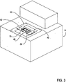
本発明のシステムは更に、プローブ15の天盤プレート22上に装着又は該プレート22と一体化された基準部材又はプレート42を含む(図2及び図3を参照)。試験ヘッド26が無いウェーハプローブ15の上面斜視図を示す図3においてより明確に図示されている基準プレート42は、天盤22によってプローブカード34上に支持される。好ましくは、基準プレート42は、図3で示されているように天盤22の中央開口上を架橋しており、更に好ましくは天盤上の中央に位置している。基準又は支持部材42は、金属又はセラミック等の何らかの好適な材料から作られた厚肉の高度に平坦なプレートとすることができる。基準部材42は、好ましくは平面を定める特徴部を有し、これは好ましくは基準部材42の下面にある。このような特徴部は、天盤22に対して平坦であり、従ってチャック30の上面32に対して平行且つ平坦であって、好ましくは平坦な底面44である。基準面44において高い平坦度を達成するために、好ましくは、基準プレート42は、例えば鋼鉄又はアルミニウムのような金属である剛性材料で作られる。アクセス開口46は、試験ヘッド26の電気インターフェース36が下にあるプローブカード34にアクセスすることができるように、基準プレート42と天盤22との間に設けられる。
The system of the present invention further includes a reference member or
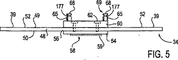
プローブカード34は、ウェーハプローブによって担持され、試験システム20の1つ又はそれ以上の試験ヘッド26と試験中のウェーハ33のダイとの電気的インターフェースを提供する(図2を参照)。プローブカード34は基板層を含み、該基板層は、どのような好適な誘電材料から作ることもでき、好ましくは第1の面又は上面49と反対側の第2の面又は底面50とを有するプリント回路基板(PCB)48である(図4及び図5を参照)。複数のコンタクトパッド39は、PCB48の上面49上に形成され、好ましくはプローブカード34の周辺部分52に配置される。図4にその幾つかが示されているコンタクトパッド39は、1つ又はそれ以上のパターンで配列され、プローブカード34の上部からアクセス可能である。試験ピン38のコンタクトパッド39との接触及び位置合わせを可能とするために、試験ヘッド26の複数の試験ピン38は、コンタクトパッド39のパターンに対応する1つ又はそれ以上のパターンで配列される。複数の異なるアレイを含むコンタクトパッド39は、プローブカード34の周辺部分52の周りを部分的に又は完全に延びることができる。従って、図4において示される2つの側部に沿うなどの周辺部52の一部にだけ配置されたコンタクトパッド39を有するカード34を対象とする程度に本発明が十分広範囲であることは明らかである。プローブカード34は更に、例えばセラミック又は他の好適な材料から作られ、PCB48の底面50に固定又は堅固に結合され、且つプローブカード34の中央部分56内に配置されたブロック54である基板部材を含むことができる。好ましくは、カード34の中央部分56は、コンタクトパッド39の内側にあるカード34の部分であり、更に好ましくは基準プレート42の中央部分の下にあるカード34の部分である。
The
プローブアレイ又は組立体58は、プローブアレイ58を支持する中央に配置されたブロック54から吊下又は垂下する(図5を参照)。プローブアレイ58のプローブ要素又はプローブ59は、試験中のダイのコンタクトボンディングパッド又はボールのパターンに対応するパターンで配列される。プローブ59の各々は、プローブアレイ58がウェーハ33に係合するときに、ダイのコンタクトパッドと位置合わせされて係合するプローブエンド又は先端を有する。プローブアレイ58のプローブ先端は、本明細書でプローブアレイ58の平面と呼ばれる場合がある平面と整列される。PCB48の上面49上のコンタクトパッド39をPCB48の下側中央部分56から吊下しているプローブアレイ58のプローブ59に電気的に結合するために、例えばPCB48内部の導電性トレース(図示せず)である電気リード部がプローブカード34に設けられる。
The probe array or
好ましくは、プローブカード34は更に、プローブカード34の中央部分56内においてPCB48の上面49に取付けられた補強部材又はプレートを含む(図4及び図5を参照)。好ましくは、補強プレート60は、金属等のあらゆる好適な剛性材料で作られ、ねじ(図示せず)によってPCB48に取付けることができる。補強プレート60は、プローブカード34の中央部分56に剛性を付加する。プローブカード34は更に、プローブアレイ58の平面、具体的にはプローブ59の先端で形成される平面を補強プレート60の平面に対して調節するための3つ又はそれ以上の平坦化調節ねじ62を含む。更に具体的には、ねじ62により、プローブアレイ58の平面を補強プレート60の平面に実質的に平行にすることが可能となる。
Preferably, the
プローブカード34の中央部分、及び好ましくは補強プレート60は、平面を定める特徴部を含む。好ましくは、当該特徴部は、少なくとも3つである複数のアライメント要素65であり、プローブカード34の中央部分56内において補強プレート60に取付けられ、プローブカード34から外方、好ましくは上向きに延びる(図4及び図5を参照)。アライメント要素65は、上面68を有し、該上面68が実質的に平面を定めるように補強プレート60上に配列される。図4に示されているように、アライメント要素65は三角形状、好ましくは平面図において正三角形を形成するように離間して配置される。好ましくは、アライメント要素65は高精度に機械加工可能な金属から作られる。アライメント要素の上面68によって形成される平面は、平面を定めるプローブカードの特徴部であり、プローブアレイ58の平面、及び好ましくは補強プレート60の平面に実質的に平行であるのが好ましい。
The central portion of the
平面を定めるプローブカード34の特徴部を基準部材42に対して、好ましくは平面を定める基準部材42の特徴部に対して押しつけるための手段又は協動機構部が含まれる。例示された実施形態では、当該手段又は装置69は、アライメント要素65を含み、プローブ59によって形成される平面を基準プレート42の底面44に対して平坦又は平行にする役割を果たす。装置69は、プローブカード34の中央部分を基準部材42に対して堅固に結合するために、基準部材42及びプローブカード34の中央部分によって担持される本発明の協動機構部の一部とすることができる。好ましくは、当該協動機構部及び装置69は、プローブカード34のアライメント要素65を基準プレート42にラッチするために、基準プレート42に装着されるラッチング機構部70を含む。好ましくは、ラッチング機構部70は、アライメント要素65の上面68を基準プレート42の底部平坦面44に対して持ち上げて押しつける。ラッチング機構部70は、ウェーハプローブ15に、好ましくはその天盤22に堅固に結合される。本明細書に例示された1つの好ましい実施形態では、ラッチング機構部は、基準プレート42にボルト又は他の方法で堅固に固定される。
Means or cooperating mechanisms are included for pressing the features of the
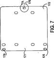
本発明の1つの実施形態によるグリッピング又はラッチング機構部70は、第1の表面又は上面172及び反対側の第2の表面又は底面173を有するラッチ部材又はプレート171を含む(図6及び図7を参照)。それぞれのアライメント要素65の少なくとも一部分を係合又は受取るように適合された複数の孔又はスロット176は、ラッチングプレートの表面172及び173を通って延びる。好ましくは、アライメント要素又はラッチピン65は、プレート171による要素65のラッチングを容易にするために、アライメント要素の円筒本体の周りを延びる環状溝177等の凹部を備えたキノコ形ラッチピンの形状である(図2及び図9を参照)。各鍵孔スロット176は、アライメント要素65のヘッド179が通過するのに十分大きな拡大開口部178と、アライメント要素65の溝177に滑入してアライメント要素65を該要素65のヘッド179の下で係合する内側リッジ180とを含む。
The gripping or latching
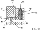
グリッピング又はラッチング組立体又は機構部170は更に、図8及び図9に示されているようにラッチプレート171の上に位置付けられた昇降プレート182を含む。ラッチプレート171の側部分184は、図8に示されているように昇降プレート182を越え、図8では仮想線、図9では実線で示されているウェーハプローブ15の基準プレート42の下まで延びる。鍵孔スロット76は、ラッチプレート171の側部分184内に配置されており、従って、上にある昇降プレート182によって覆われない。昇降プレート182は、6つの機械式カプラー又はファスナー185によって下にあるラッチプレート171に機械的に結合される。ラッチング機構部70は、図8において概略的に示されているようにアクチュエータ又は機構部186を含み、これは昇降プレート182に機械的に結合され、昇降プレート182及び昇降プレート182に機械的に結合されたラッチプレート171を水平方向及び上方向に移動させる。アクチュエータは、空気圧式、油圧式、電気式、又は上記のどれかの組合せといったどのような好適なタイプのものであってもよい。
The gripping or latching assembly or mechanism 170 further includes a
図9にその1つが幾らか詳細に例示されている各機械式カプラー185は、好ましくは昇降プレート182を通って延びるI字形の本体又はピン187から成る。ピン187は、ばね191に接して着座されたフランジ状の上端189と、ラッチプレート171内に形成されスロット176と同様に鍵形スロット195内に着座されたフランジ状の下端とを有する。好ましくは、ばね191は、ピン187の周りに同心状に延び、昇降プレート182内に形成されたキャビティ又はボア196内に着座又は配置された皿型ワッシャの好適な積み重ねである。ばね191は、第1又は上端をピン187の上端189に対して載置又は押し付け、及び第2又は下端をキャビティ192の底部を形成するフランジ196の内面に対して載置又は押し付けることにより、ピン187を付勢する。
Each
図10は、ウェーハプローブ15の基準プレート42に対するラッチング機構部70の平面図を示している。昇降プレート182は、基準プレート42の開口194内に位置付けられる。ラッチプレート171の側部分184は、基準プレート42の下に位置付けられ、従って図10では見ることはできず、側部分184内に設置された鍵孔スロット176を基準プレート42の低い平坦面44の下に位置付けるようになる。図9は、基準プレート42の低い平坦面44の下にある鍵孔スロット176の1つを示している。
FIG. 10 is a plan view of the
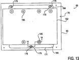
装置69の動作及び使用方法においては、ラッチング機構部70は、アライメント要素65に係合して上向きに持ち上げて、アライメント要素65の上面68を基準プレート42の底部平坦面44に対して押しつける。装置69を利用したラッチシーケンスを、図8〜図17を参照しながら説明する。始めに操作者は、アクセスドア24を使用して、プローブカード34をウェーハプローブ内に装荷する。プローブカード34は、該プローブカード34の一部分しか示されていない図9において図示されている位置と同様のラッチング機構部70の下にある位置にプローブカードを送出するウェーハプローブ(図示せず)の内部機構部上に載置される。当該内部機構部は、図8及び図9に例示されているように要素65を鍵孔スロット176の大きな開口178と整合し、次いで、図11及び図12に例示されているように、アライメント要素65を引き上げて、要素65の溝177が鍵穴176の内側リッジ180と整合するようにする。次に昇降プレート182は、上記で言及したアクチュエータ186によって水平方向に滑動され、これにより昇降プレート182に結合されたラッチプレート171を水平方向に滑動させる。これにより鍵孔スロット176の内側リッジ80がアライメント要素65の環状溝177に係合するようになる(図13及び図14を参照)。次いで、昇降プレート182は、アクチュエータによって情報に引き上げられ、これにより、アライメントセグメント65のヘッド179上の上面68の全てが基準プレート42の底部平坦面44に係合するまでラッチプレート171を上方に持ち上げる(図15及び16を参照)。プローブカード34は、ダイのボンディングパッドがプローブカード34のそれぞれのプローブ要素又はプローブ59に接触するように、チャック30にウェーハ33を機械的に位置付けさせることにより、ダイに電気的に接続される。
In operation and use of the
アライメント要素65の上面68の全てが基準プレート42と係合した場合に、ラッチプレート171の上面が基準プレートの底面44に平行でないといった、プレート171とプレート182との間の何らかの不整合に適応する必要に応じて、カプラー185を使用したラッチプレート171の昇降プレート182への非剛性的な取付けにより、該ラッチプレートを昇降プレートから分離することが可能となる。更に具体的には、カプラー185の各々は、それぞれのキャビティ192内で遊動することができ、プレート171とプレート182との間のこのような運動が許容される。ばね191は、カプラー185のフランジ状上端189に対して押しつけ又は押すように機能し、昇降プレート182に対するラッチプレート171のこうしたどのような運動にも関係なく、アライメント要素65の上面168を基準プレート42の平坦面に対して絶えず押しつけるようになる。このような各ばね力の量は、リフトプレート182内でばね191が最初に圧縮されている量を調節することにより予め定めることができる。好ましくは、アライメント要素65は、システム14の動作中の基準プレート42に対するアライメント要素65、及びそれに取付けられたプローブカード34の並進並びに回転を阻止するように平坦面44に対して十分な力で押しつけられる。
When all of the
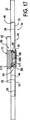
図17は、装置69及びそのラッチング機構部70を使用して基準プレート42に、従ってウェーハプローブ15に取付けられたプローブカード34を示している。図17並びに図16に示されているように、プローブカード34が上述の基準プレートに関連付けられ付加された時に、間隙196がラッチプレート171の底面と補強プレート60の上面との間に存在する。望ましくは、間隙196は、システム14の動作以前から存在する可能性があり、又はシステム14の動作中にプローブカード34が受ける温度変化又は機械的力の結果として出現する可能性がある補強プレート60と基準プレート22との間の何らかの不規則性、不整合、又は平坦性の欠如にも適応する。
FIG. 17 shows the
理解されるように、本発明の装置69及び方法は、基準プレート42の底部平坦面44、従ってチャック30の上面32に対してアライメント要素65の上面68を平坦化するよう機能する。プローブアレイ58の平面は、アライメント要素65の上面68の平面に対して平坦であり、当該上面68の平面は基準プレート42の平坦面44に対して押しつけられた時に、チャック30の平面に対して平坦であるので、プローブアレイ58の平面は、チャック30の平面に対して平坦であり、ウェーハ33上のダイとのプローブアレイ58の適正な係合、すなわち当該ダイの正確な試験を容易にする。従って、ラッチ状態においては、ラッチング機構部70は、チャック30に対して平坦なプローブカード34の中央部分56を堅持する。
As will be appreciated, the
本発明のシステムは、従来技術よりも優れた利点を提供する。1つの利点は、プローブカード34の中央部分56の外側のプローブカードの変形は、中央部分56が基準プレート42によって平坦に保持されるので、プローブアレイ58の平坦化にほとんど影響を与えないことである。図18は、プローブカード34のPCB48の変形がプローブアレイ58の平坦化にどのように影響を与えないかを示している。すなわち装置69によって、プローブアレイ58の平坦性を保つためにプローブカード34の中央部分56を越えて延びる補強プレートを備える必要性が低減され、これによりプローブカード34の重量を低減することができる。
The system of the present invention provides advantages over the prior art. One advantage is that deformation of the probe card outside the
別の利点は、基準プレート42が中央部分56を基準プレート42に対して平坦に保持することによって、プローブカード34の中央部分56に剛性が付加されることである。更に、基準プレート42は、間隙96によってプローブカード34から熱的に絶縁されているため、アライメント要素65を通じた熱伝導を無視できると仮定すると、基準プレート42はプローブカード34の熱質量を増加させない。従って、基準プレート42は、ウェーハの温度試験中の熱変形の影響が有意に少ない。熱質量は、ウェーハの温度試験中にプローブカード34の温度が安定化するのに必要な時間を低減させるので重要である。
Another advantage is that the
装置69及び本発明の方法は、プローブカード34の中央部分56を架橋支持部材42に、従ってウェーハプローブ15に堅固に結合又は固定するのに役立つ。好ましい実施形態においては、プローブカード34の周辺部分52は、基準プレート42が無く、基準プレート42又はウェーハプローブ15により支持されていない。上述のことにも関わらず、本発明は、例えばプローブカード34の支持とは異なる目的で、ウェーハプローブがプローブカード34の周辺部分52の幾らかの小部分又はほんの小さな割合に接触する場合の方法及び装置を対象とするのに十分に広範囲である。本発明はまた、プローブカード34の重量の主要部分又はかなりの部分、或いは大部分がカード34の中央部分56によって支持されている限り、プローブカード34の周辺部分52の幾らかの小部分又はほんの小さな割合が、基準プレート42又はプローブ天盤22によってなど、ウェーハプローブにより支持される場合の方法及び装置を対象とするのに十分に広範囲である。
The
プローブカード34を中央部分56によって実質的又は好ましくは単独で支持することは、有利には、他の目的のためにプローブカード34の周辺部分52を開放する役割を果たす。例えば、プローブカードの周辺部分52に支持ピン又は他の支持構成要素を含まないことにより、試験ヘッド36がプローブカード34と係合することができる方法及び手段を拡張することができる。
Supporting the
本発明を用いて、円形及び他の非矩形プローブカードを含む、様々なタイプのプローブカードのプローブアレイを平坦化することができる。プローブカードを平坦化する本発明の装置の別の実施形態においては、円形プローブカード234に用いるための基準プレート242が提供される。図19及び図20において、ウェーハプローブ215の円形天盤222上に示されている基準プレート242は中央部分245を有し、そこからスポーク247が延びて円形天盤222に取付けられるか又は一体化される。スポーク247は、基準プレート242を円形プローブカード234の上に堅固に支持し、プローブカード234の周辺部分252が、基準プレート242の下にあるように図19に示されている。コンタクトパッド239は、カード234の基板層又はプリント回路基板248の上面に備えられる。簡明化のために、図19ではコンタクトパッド239の単一のアレイのみが示されている。適正に構成された試験ヘッド36が、下にあるプローブカード234、具体的にはその上のコンタクトパッド239にアクセスできるように、スポーク247はこれらの間にアクセス開口249を備えるように配列される。上述のラッチング機構部70及び基準平坦面44と同様のラッチング機構部及び基準平坦面(図示せず)は、基準プレート242の中央部分245に設置される。
The present invention can be used to planarize probe arrays for various types of probe cards, including circular and other non-rectangular probe cards. In another embodiment of the apparatus of the present invention for planarizing a probe card, a
図21に平面で示されている円形プローブカード234は、プローブカード234の中央部分256内にある補強プレート260と、プローブカード234の周辺252に沿って環形に配列されたコンタクトパッド239の例示的なアレイ240を含む。図示されてはいないが、上述のプローブアレイ58と同様のプローブアレイは、中央部分256内においてプローブカード234の底部から吊下する。上述のアライメント要素65と実質的に同様とすることができる3つ又はそれ以上のアライメント要素265は、中央部分256内において補強プレート260に取付けられ、プローブカード234から上方に延びる。アライメント要素265は、上述の方法で基準プレート242と協動し、プローブアレイをウェーハプローブ215のチャック(図示せず)の上面に対して平坦化又は平行にする。更に具体的には、アライメント要素265の上面は、基準プレート242の底部平坦面に対し押しつけられる。
A
上述のことから、本発明の基準部材又はプレートは、どのような寸法及び形状のプローブカードにも適応するように構成し成形することができる点を理解されたい。上述のように、例えば基準プレートは、平面図で矩形又は円形とすることができる。基準プレートの下に位置付けられたプローブカードのコンタクトパッドへのアクセスを可能とするために、どのような好適な構成においても、基準プレートに開口又は開孔を設けることができる。例えば、円形基準プレート242にはスポークが備えられ、これらのスポークは、円形プローブカード234上に備えられたコンタクトパッド239のアレイにアクセスするため、該スポーク間に開口を定める。
From the foregoing, it should be understood that the reference member or plate of the present invention can be configured and molded to accommodate any size and shape of probe card. As described above, for example, the reference plate can be rectangular or circular in plan view. In any suitable configuration, an opening or aperture can be provided in the reference plate to allow access to the contact pads of the probe card positioned below the reference plate. For example, the
上述において言及した平面を定める基準部材の特徴部は、平坦面に限定されず、どのような好適な構成のものであってもよい点は明らかである。例えばこうした特徴部は、上述の要素65のような複数の離間された外方に延びるアライメント要素とすることができる。同様に、平面を定めるプローブカードの特徴部は、上述の離間された外方に延びる構成要素65に限定されず、どのような好適な構成のものであってもよい。従って、例えば、上述のアライメント要素65のような外方に延びるアライメント要素は、上述のように補強プレート60上ではなく、基準部材又はプレート42上、或いは別のウェーハプローブ上に備えることができる。例えばアライメント要素が基準プレート42から吊下しており、チャック30の上面32に対して平行な平面を定める端面を有する場合には、平坦な基準面は、例えばプローブアレイ58の平面に対して平行な補強プレート60の上面としてプローブカード上に備えられる。例えば、ラッチング機構部70と同様のラッチング組立体又は機構部は、機構部70に関する上述の方法基準部材のアライメント要素を把持するために、プローブカードの中央部分の上部に装着することができる。或いは、アライメント要素が基準部材又はウェーハプローブ上の他の何所かに備えられる場合には、補強プレート60又はプローブカードの中央部分上の他の何所かから上方に延びる結合構成要素の1セットを把持するために、ラッチング組立体又は機構部は、ウェーハプローブ、例えば上述の基準部材42に堅固に結合することもできる。従ってこのような実施形態は、基準部材から吊下しているアライメント要素、及び、例えばアライメント要素65と同様の補強プレート60から直立している結合要素を有すことができる。更に、本発明のあらゆる基準平面は、単一の表面、又は単一の面に延びる異なる表面のセットから形成することができる点は理解される。
It is obvious that the characteristic part of the reference member that defines the plane referred to above is not limited to a flat surface and may have any suitable configuration. For example, such features can be a plurality of spaced outwardly extending alignment elements, such as
本発明の装置のアライメント要素の上面を基準プレートの底部平坦面に押しつけるために、好ましい実施形態においてはラッチング機構部を利用したが、他の手段を利用してもよい。例えば、アライメント要素の上面が基準プレートの底部平坦面に対して当接するように、プローブカード全体を基準プレートに向けて引き上げることができる。これは、例えば、プローブカードを上下させることができる可動プレートにプローブカードを固定することによって行うことができる。プローブカードは、その周辺部分又は他のあらゆる部分において掴み、クランプし、或いは動かすことができる。 In order to press the upper surface of the alignment element of the apparatus of the present invention against the bottom flat surface of the reference plate, the latching mechanism is used in the preferred embodiment, but other means may be used. For example, the entire probe card can be raised toward the reference plate such that the top surface of the alignment element abuts against the bottom flat surface of the reference plate. This can be done, for example, by fixing the probe card to a movable plate that can move the probe card up and down. The probe card can be grasped, clamped or moved in its peripheral part or any other part.
本発明の一態様では、中央部分及び周辺部分を備えた基板層と該基板層の中央部分に装着された吊下プローブ組立体とを有し、第1の平面において実質的に延びるそれぞれのプローブ先端を備えた複数のプローブ要素と基板層の上からアクセス可能であり且つプローブ要素への電気的接続を可能にするためにそれぞれのプローブ要素に電気的に結合されたコンタクト要素のアレイとを更に有するプローブカードで使用し、並びにウェーハプローブで使用するための装置が提供される。該装置は、第2の平面を定める特徴部を有し且つ第2の平面が第1の平面に対して実質的に平行になるように基板層の中央部分の上に装着するよう適合されている補強部材と、ウェーハプローブに装着するよう適合され且つ第3の平面を定める特徴部を備えた下面を有する基準部材とを含むことができ、第2の平面を定める補強部材の特徴部が第3の平面を定める基準部材の特徴部に押しつけられた時に、第1の平面が第3の平面に対して実質的に平行に延びて、プローブ先端がウェーハプローブに対して実質的に平坦化されるようになる。 In one aspect of the invention, each probe has a substrate layer having a central portion and a peripheral portion and a suspended probe assembly attached to the central portion of the substrate layer and substantially extending in a first plane. A plurality of probe elements with tips and an array of contact elements accessible from above the substrate layer and electrically coupled to each probe element to allow electrical connection to the probe elements; An apparatus for use with a probe card as well as for use with a wafer probe is provided. The apparatus has a feature defining a second plane and is adapted to be mounted over a central portion of the substrate layer such that the second plane is substantially parallel to the first plane. And a reference member having a lower surface adapted to be attached to the wafer probe and having a lower surface defining a third plane, wherein the reinforcing member feature defining the second plane is first. When pressed against a feature of the reference member defining three planes, the first plane extends substantially parallel to the third plane and the probe tip is substantially planarized with respect to the wafer probe. Become so.
このような装置は、天盤を有するウェーハプローブに用いるためのものとすることができ、基準部材は、天盤上を架橋するように構成することができる。第3の平面を定める基準部材の特徴部は、第3の平面で実質的に延びる底面とすることができ、又は第3の平面を定める基準部材の特徴部は、実質的に第3の平面を定めるそれぞれの端面を有する、少なくとも3つである複数の離間して下方に延びるアライメント要素とすることができる。第2の平面を定める補強部材の特徴部は、実質的に第2の平面を定めるそれぞれの端面を有する、少なくとも3つである複数の離間して上方向に延びるアライメント要素とすることができ、このような装置は更に、端面が第3の平面を定める基準部材の特徴部に係合するようにアライメント要素に係合して移動させるため、及びアライメント要素の端面を基準部材の当該特徴部に対して維持するために基準部材によって担持される把持組立体を更に含むことができる。当該装置は、第2の平面を定める補強部材の特徴部を第3の平面を定める基準部材の特徴部に対して押しつけるための手段を含むことができ、押しつけ手段は基準部材によって担持することができる。基板層は、プリント回路基板とすることができる。 Such an apparatus may be for use with a wafer probe having a top and the reference member may be configured to bridge the top. The feature of the reference member that defines the third plane can be a bottom surface that extends substantially in the third plane, or the feature of the reference member that defines the third plane is substantially the third plane. There may be a plurality of spaced apart, downwardly extending alignment elements, each having an end face defining at least three. The reinforcing member feature defining the second plane can be at least three spaced apart upwardly extending alignment elements having respective end faces that substantially define the second plane; Such a device is further adapted to engage and move the alignment element such that the end face engages a feature of the reference member defining a third plane, and the end face of the alignment element to the feature of the reference member. It may further include a gripping assembly carried by the reference member to maintain against. The apparatus can include means for pressing the feature of the reinforcing member defining the second plane against the feature of the reference member defining the third plane, the pressing means being carried by the reference member. it can. The substrate layer can be a printed circuit board.
本発明の別の態様では、基準部材とウェーハ上の集積回路を試験するためのテスタとを備えた天盤を有するウェーハプローブに用いるためのプローブカードが提供される。プローブカードは、中央部分及び周辺部分、並びに上面及び底面を有する基板層と、該基板層の中央部分から吊下して集積回路に係合するよう適合された複数のプローブ要素を有するプローブ組立体であって、該プローブ要素が実質的に第1の平面で延びるそれぞれのプローブ先端を備えたプローブ組立体と、基板層の周辺部分の上面にあり、プローブ要素との電気的接続を可能にするためにそれぞれのプローブ要素に電気的に結合されたコンタクト要素のアレイと、基板層の中央部分上に装着され、第1の平面に対して実質的に平行な第2の平面を定める特徴部を有する補強部材とを含むことができ、第2の平面を定める補強部材の特徴部が基準部材に対して押しつけられた時に、プローブ先端の第1の平面がウェーハプローブに対して実質的に平坦化される。 In another aspect of the invention, a probe card is provided for use in a wafer probe having a roof with a reference member and a tester for testing an integrated circuit on the wafer. A probe card includes a substrate layer having a central portion and a peripheral portion, and a top surface and a bottom surface, and a plurality of probe elements adapted to hang from the central portion of the substrate layer and engage an integrated circuit. A probe assembly with a respective probe tip extending substantially in a first plane and on the upper surface of the peripheral portion of the substrate layer to allow electrical connection with the probe element An array of contact elements electrically coupled to each probe element and a feature mounted on a central portion of the substrate layer and defining a second plane substantially parallel to the first plane. And a reinforcing member defining a second plane is pressed against the reference member so that the first plane of the probe tip is effective against the wafer probe. To be flattened.
第2の平面を定める補強部材の特徴部は、実質的に第2の平面を定めるそれぞれの端面を有する、少なくとも3つである複数の離間して上方に延びるアライメント要素とすることができ、該アライメント要素はピンとすることができる。アライメント要素は、平面で見たときに三角形状を形成するように離間して配置することができる。 The reinforcing member feature defining the second plane can be at least three spaced apart upwardly extending alignment elements having respective end faces that substantially define the second plane, The alignment element can be a pin. The alignment elements can be spaced apart to form a triangular shape when viewed in a plane.
本発明の別の態様では、ウェーハ上の集積回路を試験するテスタに用いるためのウェーハプローブが提供される。ウェーハプローブは、基準部材を備える天盤を有し且つウェーハを担持するよう適合された上平坦面を有するチャックを備えたハウジングであって、該基準部材がその少なくとも1つの表面によって定められ且つチャックの上面に対して実質的に平行な第1の平面を有する該ハウジングと、非導電材料から形成された基板層を有し且つチャックの上にあるプローブカードであって、基板層が中央部分及び周辺部分並びに上面及び底面を有する該プローブカードと、基板層の中央部分の底面上に装着され且つ集積回路に係合するように適合された複数のプローブ要素を有するプローブ組立体であって、プローブ要素が実質的に第2の平面で延びるそれぞれのプローブ先端を備えた該プローブ組立体と、基板層の中央部分上に装着された補強プレートであって、該補強プレートの少なくとも1つの表面によって定められ且つ第2の平面に対して実質的に平行な第3の平面を有する該補強プレートとを含むことができ、基準部材の少なくとも1つの表面及び補強プレートの少なくとも1つの表面のうちの一方が、少なくとも3つである複数の離間して外方に延びるアライメント要素の端面であり、基準部材の少なくとも1つの表面及び補強プレートの少なくとも1つの表面のうちの他方が、平面で延びる表面であり、補強プレートが基準プレートに対して押しつけられた時に、アライメント要素の端面が平面において延びる表面と係合し、プローブ先端の第2の平面がチャックの上面に対して実質的に平行となる。 In another aspect of the present invention, a wafer probe is provided for use in a tester that tests an integrated circuit on a wafer. A wafer probe is a housing having a top with a reference member and a chuck having an upper flat surface adapted to carry a wafer, the reference member being defined by at least one surface thereof and the chuck A probe card having a first plane substantially parallel to the upper surface of the substrate and a substrate layer formed from a non-conductive material and overlying the chuck, wherein the substrate layer comprises a central portion and A probe assembly comprising: a probe card having a peripheral portion and a top surface and a bottom surface; and a plurality of probe elements mounted on the bottom surface of the central portion of the substrate layer and adapted to engage an integrated circuit, A probe assembly having a respective probe tip with elements extending substantially in a second plane, and a reinforcing plate mounted on a central portion of the substrate layer; The reinforcing plate having a third plane defined by at least one surface of the reinforcing plate and substantially parallel to the second plane, and at least one of the reference members One of the at least one surface and the at least one surface of the reinforcing plate is an end face of a plurality of spaced outwardly extending alignment elements, and at least one of the reference member and at least one of the reinforcing plate The other of the two surfaces is a surface extending in a plane, and when the reinforcing plate is pressed against the reference plate, the end face of the alignment element engages the surface extending in the plane, and the second plane of the probe tip is It is substantially parallel to the upper surface of the chuck.
当該ウェーハプローブは、アライメント要素を平面において延びる表面に対して把持し且つ押しつけるために、基準部材及び補強プレートの一方によって担持される把持組立体を含むことができる。把持組立体は、基準部材によって担持することができ、アライメント要素を捕捉し把持するように構成された機構部を含むことができる。当該ウェーハプローブの基準部材は、少なくとも3つである複数の離間して外方に延びるアライメント要素を有することができ、又は当該ウェーハプローブの補強プレートは、少なくとも3つである複数の離間して外方に延びるアライメント要素を有することができる。 The wafer probe can include a gripping assembly carried by one of the reference member and the reinforcing plate to grip and press the alignment element against a surface extending in a plane. The gripping assembly can be carried by the reference member and can include a mechanism configured to capture and grip the alignment element. The reference member of the wafer probe may have at least three spaced outwardly extending alignment elements, or the wafer probe reinforcing plate may be at least three spaced apart outer members. There may be an alignment element extending in the direction.
本発明の別の態様では、吊下プローブ組立体を備えた中央部分及び平面を定める特徴部を有するプローブカードに用いるため、及び基準部材を有する天盤を備えるウェーハプローブに用いるための方法が提供される。方法は、平面を定めるプローブカードの中央部分にある特徴部を基準部材に対して押しつけてプローブ組立体をウェーハプローブに対して整合する段階を含むことができる。 In another aspect of the present invention, a method is provided for use in a probe card having a central portion with a suspended probe assembly and a planar defining feature and for use with a wafer probe with a roof having a reference member. Is done. The method can include pressing a feature in a central portion of the probe card defining a plane against a reference member to align the probe assembly with the wafer probe.
当該方法は、プローブカードの中央部分をウェーハプローブに固定する段階を含むことができる。平面を定めるプローブカードの特徴部は、実質的に平面を定めるそれぞれの端面を有する、少なくとも3つである複数の離間して上方に延びるアライメント要素とすることができる。基準部材は、平面において実質的に延びる底面を有することができ、押しつけ段階は、平面を定めるプローブカードの特徴部を基準部材の底面に対して押しつける段階を含むことができる。平面を定めるプローブカードの特徴部は平坦面とすることができる。 The method can include securing a central portion of the probe card to the wafer probe. The features of the probe card that define a plane can be a plurality of spaced apart upwardly extending alignment elements having respective end surfaces that define a substantially plane. The reference member can have a bottom surface that extends substantially in a plane, and the step of pressing can include pressing a feature of the probe card that defines the plane against the bottom surface of the reference member. The feature of the probe card that defines the plane can be a flat surface.
本発明の別の態様では、天盤を有するウェーハプローブに用いるための装置が提供される。装置は、天盤上において該天盤を架橋する位置で装着するよう適合された支持部材と、中央部分及び周辺部分を有し且つ該中央部分から吊下しているプローブ組立体を有するプローブカードと、プローブカードを支持部材に堅固に結合するために、支持部材及びプローブカードの中央部分によって担持される協動機構部とを含むことができる。 In another aspect of the invention, an apparatus is provided for use with a wafer probe having a roof. The apparatus comprises a probe card having a support member adapted to be mounted on the top of the roof in a position to bridge the top, and a probe assembly having a central portion and a peripheral portion and suspended from the central portion And a cooperating mechanism carried by the support member and the central portion of the probe card to securely couple the probe card to the support member.
プローブカードは、基板層を有することができ、協動機構部は、基板層の上に装着された補強部材を含むことができる。協動機構部は、支持部材に堅固に結合されたラッチング機構部を含むことができる。 The probe card can have a substrate layer, and the cooperation mechanism can include a reinforcing member mounted on the substrate layer. The cooperating mechanism can include a latching mechanism that is rigidly coupled to the support member.
本発明の更なる態様では、中央部分及び周辺部分を有するプローブカードをウェーハプローブに固定するための方法が提供される。該方法は、プローブカードの中央部分をウェーハプローブに固定する段階を含むことができ、該プローブカードの周辺部分はウェーハプローブが存在しない。 In a further aspect of the invention, a method is provided for securing a probe card having a central portion and a peripheral portion to a wafer probe. The method can include securing a central portion of the probe card to a wafer probe, and a peripheral portion of the probe card is free of wafer probes.
当該方法は、基準部材を備えたプローブ天盤を有するウェーハプローブに用いるものとすることができ、固定段階は、プローブカードの中央部分を基準部材に固定する段階を含むことができる。 The method may be used for a wafer probe having a probe top with a reference member, and the fixing step may include fixing a central portion of the probe card to the reference member.
上述のことから明らかであるように、特にプローブカードの下面に装着されたプローブアレイの近傍において、プローブカードの変形を最小限に抑えるプローブカードを平坦化する装置が提供されてきた。装置は、プローブカードの下面に備えられたプローブアレイの平坦性をウェーハプローブの基準プレートと整合させるために、プローブカードの中央部分に配置された複数の、好ましくは少なくとも3つである複数のアライメント要素を含むことができる。アライメント要素は、ラッチング機構部で掴むことにより、又はプローブカードの他のいずれかの部分に係合することにより基準プレートの基準面に対して押しつけて、そこに固定されたアライメント要素を基準プレートに対して押しつけるようにすることができる。 As is apparent from the above, there has been provided an apparatus for flattening a probe card that minimizes deformation of the probe card, particularly in the vicinity of the probe array mounted on the lower surface of the probe card. The apparatus includes a plurality of, preferably at least three, alignments arranged in the central portion of the probe card to align the flatness of the probe array provided on the lower surface of the probe card with the reference plate of the wafer probe. Can contain elements. The alignment element is pressed against the reference surface of the reference plate by gripping it with a latching mechanism or by engaging any other part of the probe card, and the alignment element fixed thereto is brought into contact with the reference plate. It can be pressed against.
14 ウェーハ試験システム
15 ウェーハプローブ
19 制御装置
20 自動試験システム
22 天盤
24 アクセスドア
26 試験ヘッド
14
Claims (13)
前記装置が、
第2の平面を定める特徴部を有し、前記基板層の中央部分に剛性を付加するために前記基板層の中央部分の上に装着するよう適合された補強部材と、
前記ウェーハプローブに装着するよう適合され且つ第3の平面を定める特徴部を備えた下面を有する基準部材と、
を含み、
前記第2の平面を定める前記補強部材の特徴部が前記第3の平面を定める前記基準部材の特徴部に対して押しつけられた時に、前記第1の平面が前記第3の平面に対して実質的に平行に延びて、前記プローブ先端が前記ウェーハプローブに対して実質的に平坦化されるようになり、
前記装置がさらに、
前記基準部材に装着されたラッチング機構部
を含み、
前記ラッチング機構部が、ラッチプレート、前記ラッチプレートに機械的に結合された昇降プレート、及び前記昇降プレート及び前記ラッチプレートを水平方向及び上方向に動かすために前記昇降プレートに機械的に結合されたアクチュエータを含む
ことを特徴とする装置。A plurality of substrate layers, each including a substrate layer having a central portion and a peripheral portion, and a suspended probe assembly mounted to the central portion of the substrate layer, each probe tip extending substantially in a first plane. A probe card further comprising a probe element and an array of contact elements accessible from above the substrate layer and electrically coupled to each probe element to allow electrical connection to the probe element; An apparatus for use in a wafer probe,
The device is
A reinforcing member having a feature defining a second plane and adapted to be mounted on the central portion of the substrate layer to add rigidity to the central portion of the substrate layer;
A reference member having a lower surface with a feature adapted to be attached to the wafer probe and defining a third plane;
Including
When the feature of the reinforcing member defining the second plane is pressed against the feature of the reference member defining the third plane, the first plane is substantially against the third plane. Extending in parallel to each other so that the probe tip is substantially planarized with respect to the wafer probe;
The device further comprises:
Including a latching mechanism attached to the reference member;
The latching mechanism is mechanically coupled to the lift plate for moving the latch plate, the lift plate mechanically coupled to the latch plate, and the horizontal and upward movement of the lift plate and the latch plate. An apparatus comprising an actuator.
Applications Claiming Priority (2)
| Application Number | Priority Date | Filing Date | Title |
|---|---|---|---|
| US49062103P | 2003-07-28 | 2003-07-28 | |
| PCT/US2004/024574 WO2005013332A2 (en) | 2003-07-28 | 2004-07-28 | Apparatus for planarizing a probe card and method using same |
Publications (3)
| Publication Number | Publication Date |
|---|---|
| JP2007500945A JP2007500945A (en) | 2007-01-18 |
| JP2007500945A5 JP2007500945A5 (en) | 2007-09-06 |
| JP4571133B2 true JP4571133B2 (en) | 2010-10-27 |
Family
ID=34115416
Family Applications (1)
| Application Number | Title | Priority Date | Filing Date |
|---|---|---|---|
| JP2006522082A Active JP4571133B2 (en) | 2003-07-28 | 2004-07-28 | Device for flattening probe cards |
Country Status (5)
| Country | Link |
|---|---|
| US (2) | US7098650B2 (en) |
| JP (1) | JP4571133B2 (en) |
| KR (1) | KR101181639B1 (en) |
| TW (1) | TWI351524B (en) |
| WO (1) | WO2005013332A2 (en) |
Families Citing this family (16)
| Publication number | Priority date | Publication date | Assignee | Title |
|---|---|---|---|---|
| US7262611B2 (en) * | 2000-03-17 | 2007-08-28 | Formfactor, Inc. | Apparatuses and methods for planarizing a semiconductor contactor |
| JP4951523B2 (en) * | 2005-11-15 | 2012-06-13 | 株式会社アドバンテスト | TEST HEAD, ELECTRONIC COMPONENT TESTING APPARATUS, AND METHOD FOR INSTALLING PERFORMANCE BOARD ON ELECTRONIC COMPONENT TESTING APPARATUS |
| WO2007057944A1 (en) | 2005-11-15 | 2007-05-24 | Advantest Corporation | Electronic component test equipment and method for loading performance board on the electronic component test equipment |
| US7746089B2 (en) * | 2006-09-29 | 2010-06-29 | Formfactor, Inc. | Method and apparatus for indirect planarization |
| JP2010050437A (en) * | 2008-07-25 | 2010-03-04 | Yokogawa Electric Corp | Ic tester |
| JP2010175507A (en) | 2009-02-02 | 2010-08-12 | Micronics Japan Co Ltd | Electrical connection device |
| KR101278890B1 (en) * | 2009-07-30 | 2013-06-26 | 가부시키가이샤 아드반테스트 | Probe card holding apparatus and prober |
| US8278956B2 (en) * | 2010-04-08 | 2012-10-02 | Advantest America, Inc | Probecard system and method |
| JP5952645B2 (en) * | 2012-06-06 | 2016-07-13 | 東京エレクトロン株式会社 | Wafer inspection interface and wafer inspection apparatus |
| WO2014002078A1 (en) * | 2012-06-29 | 2014-01-03 | Hydrovision Asia Pte Ltd | An improved suspended sediment meter |
| US9134343B2 (en) * | 2012-09-28 | 2015-09-15 | Intel Corporation | Sort probe gripper |
| KR101255113B1 (en) | 2012-10-31 | 2013-04-19 | 주식회사 프로이천 | Method of manufacturing probe block having an absorber |
| JP6042761B2 (en) * | 2013-03-28 | 2016-12-14 | 東京エレクトロン株式会社 | Probe device |
| JP6184301B2 (en) * | 2013-11-14 | 2017-08-23 | 株式会社日本マイクロニクス | Inspection device |
| KR102566685B1 (en) | 2016-07-18 | 2023-08-14 | 삼성전자주식회사 | Apparatus for clamping a probe card and probe card including the same |
| US11022628B2 (en) | 2019-09-13 | 2021-06-01 | Reid-Ashman Manufacturing, Inc. | Probe card support apparatus for automatic test equipment |
Family Cites Families (20)
| Publication number | Priority date | Publication date | Assignee | Title |
|---|---|---|---|---|
| US3810016A (en) * | 1971-12-17 | 1974-05-07 | Western Electric Co | Test probe for semiconductor devices |
| US4038599A (en) * | 1974-12-30 | 1977-07-26 | International Business Machines Corporation | High density wafer contacting and test system |
| JPS6362245A (en) * | 1986-09-02 | 1988-03-18 | Canon Inc | Wafer prober |
| JPH0833433B2 (en) | 1987-11-30 | 1996-03-29 | 東京エレクトロン株式会社 | Probe device |
| US5081415A (en) * | 1990-08-07 | 1992-01-14 | United Microelectronics Corporation | Load board insertion system |
| US5059898A (en) * | 1990-08-09 | 1991-10-22 | Tektronix, Inc. | Wafer probe with transparent loading member |
| US5559446A (en) * | 1993-07-19 | 1996-09-24 | Tokyo Electron Kabushiki Kaisha | Probing method and device |
| US7064566B2 (en) * | 1993-11-16 | 2006-06-20 | Formfactor, Inc. | Probe card assembly and kit |
| US6741085B1 (en) * | 1993-11-16 | 2004-05-25 | Formfactor, Inc. | Contact carriers (tiles) for populating larger substrates with spring contacts |
| JP3135825B2 (en) * | 1995-09-27 | 2001-02-19 | 株式会社東芝 | Probe card and probing test method for semiconductor integrated circuit using the probe card |
| US6060891A (en) * | 1997-02-11 | 2000-05-09 | Micron Technology, Inc. | Probe card for semiconductor wafers and method and system for testing wafers |
| US6798224B1 (en) * | 1997-02-11 | 2004-09-28 | Micron Technology, Inc. | Method for testing semiconductor wafers |
| JPH1123615A (en) * | 1997-05-09 | 1999-01-29 | Hitachi Ltd | Connector and inspection system |
| JP3315339B2 (en) * | 1997-05-09 | 2002-08-19 | 株式会社日立製作所 | Method for manufacturing semiconductor device, method for probing to semiconductor device, and apparatus therefor |
| US6078186A (en) * | 1997-12-31 | 2000-06-20 | Micron Technology, Inc. | Force applying probe card and test system for semiconductor wafers |
| JP2001056346A (en) * | 1999-08-19 | 2001-02-27 | Fujitsu Ltd | Probe card and method for testing wafer on which a plurality of semiconductor device are formed |
| JP3343541B2 (en) * | 2000-02-18 | 2002-11-11 | 日本電子材料株式会社 | Probe card |
| DE10039336C2 (en) * | 2000-08-04 | 2003-12-11 | Infineon Technologies Ag | Method for testing semiconductor circuits and test device for carrying out the method |
| KR100347765B1 (en) * | 2000-10-18 | 2002-08-09 | 삼성전자 주식회사 | method and apparatus for inspecting a electric property in a wafer |
| TWI272394B (en) * | 2004-02-24 | 2007-02-01 | Mjc Probe Inc | Multi-function probe card |
-
2004
- 2004-07-28 US US10/902,188 patent/US7098650B2/en active Active
- 2004-07-28 JP JP2006522082A patent/JP4571133B2/en active Active
- 2004-07-28 TW TW093122605A patent/TWI351524B/en active
- 2004-07-28 WO PCT/US2004/024574 patent/WO2005013332A2/en active Application Filing
- 2004-07-28 KR KR1020067001928A patent/KR101181639B1/en active IP Right Grant
-
2006
- 2006-08-17 US US11/506,653 patent/US8120375B2/en active Active
Also Published As
| Publication number | Publication date |
|---|---|
| TW200514181A (en) | 2005-04-16 |
| US7098650B2 (en) | 2006-08-29 |
| KR20060034718A (en) | 2006-04-24 |
| KR101181639B1 (en) | 2012-09-13 |
| US20050062464A1 (en) | 2005-03-24 |
| US8120375B2 (en) | 2012-02-21 |
| TWI351524B (en) | 2011-11-01 |
| JP2007500945A (en) | 2007-01-18 |
| WO2005013332A3 (en) | 2005-12-29 |
| WO2005013332A2 (en) | 2005-02-10 |
| US20060279302A1 (en) | 2006-12-14 |
Similar Documents
| Publication | Publication Date | Title |
|---|---|---|
| US8120375B2 (en) | Method for using probe card | |
| JP5322654B2 (en) | Apparatus and method for adjusting probe orientation | |
| US20080116925A1 (en) | Probe device | |
| WO2008015962A1 (en) | Parallelism adjusting mechanism of probe card | |
| US20040104738A1 (en) | Probe card | |
| KR20050084326A (en) | Apparatus and method for limiting over travel in a probe card assembly | |
| JP2004501517A (en) | System for testing and packaging integrated circuits | |
| JPWO2008114464A1 (en) | Electrical connection device | |
| JP2005533254A (en) | Assembly for electrically connecting a device under test to a test machine for testing an electrical circuit on the device under test | |
| JP3194669B2 (en) | Inspection device and connection method in inspection device | |
| KR20100069300A (en) | Probe card, and apparatus and method for testing semiconductor device | |
| JP2000346875A (en) | Probe card and ic testing device using it | |
| KR100706228B1 (en) | Apparatus and method for testing electrical characterization of semiconductor workpiece | |
| US7256591B2 (en) | Probe card, having cantilever-type probe and method | |
| JP4941169B2 (en) | Probe card mechanism | |
| JP3224519B2 (en) | Wafer measuring jig, test head device and wafer measuring device | |
| JP2965174B2 (en) | Semiconductor device inspection equipment | |
| JP6084882B2 (en) | Probe assembly and probe board | |
| JPH11126671A (en) | Connector for ic inspection | |
| US20060060146A1 (en) | Semiconductor manufacturing apparatus and methods | |
| JPH0731185Y2 (en) | Probing device | |
| US6181148B1 (en) | Automated test head interface board locking and docking mechanism | |
| KR100906344B1 (en) | Probe card | |
| JPH0754816B2 (en) | Probe card | |
| JPH02222555A (en) | Test head for semiconductor device |
Legal Events
| Date | Code | Title | Description |
|---|---|---|---|
| A521 | Request for written amendment filed |
Free format text: JAPANESE INTERMEDIATE CODE: A523 Effective date: 20070719 |
|
| A621 | Written request for application examination |
Free format text: JAPANESE INTERMEDIATE CODE: A621 Effective date: 20070719 |
|
| A977 | Report on retrieval |
Free format text: JAPANESE INTERMEDIATE CODE: A971007 Effective date: 20100707 |
|
| TRDD | Decision of grant or rejection written | ||
| A01 | Written decision to grant a patent or to grant a registration (utility model) |
Free format text: JAPANESE INTERMEDIATE CODE: A01 Effective date: 20100712 |
|
| A01 | Written decision to grant a patent or to grant a registration (utility model) |
Free format text: JAPANESE INTERMEDIATE CODE: A01 |
|
| A61 | First payment of annual fees (during grant procedure) |
Free format text: JAPANESE INTERMEDIATE CODE: A61 Effective date: 20100811 |
|
| FPAY | Renewal fee payment (event date is renewal date of database) |
Free format text: PAYMENT UNTIL: 20130820 Year of fee payment: 3 |
|
| R150 | Certificate of patent or registration of utility model |
Ref document number: 4571133 Country of ref document: JP Free format text: JAPANESE INTERMEDIATE CODE: R150 Free format text: JAPANESE INTERMEDIATE CODE: R150 |
|
| R250 | Receipt of annual fees |
Free format text: JAPANESE INTERMEDIATE CODE: R250 |
|
| R250 | Receipt of annual fees |
Free format text: JAPANESE INTERMEDIATE CODE: R250 |
|
| R250 | Receipt of annual fees |
Free format text: JAPANESE INTERMEDIATE CODE: R250 |
|
| R250 | Receipt of annual fees |
Free format text: JAPANESE INTERMEDIATE CODE: R250 |
|
| R250 | Receipt of annual fees |
Free format text: JAPANESE INTERMEDIATE CODE: R250 |
|
| R250 | Receipt of annual fees |
Free format text: JAPANESE INTERMEDIATE CODE: R250 |
|
| R250 | Receipt of annual fees |
Free format text: JAPANESE INTERMEDIATE CODE: R250 |
|
| R250 | Receipt of annual fees |
Free format text: JAPANESE INTERMEDIATE CODE: R250 |
|
| R250 | Receipt of annual fees |
Free format text: JAPANESE INTERMEDIATE CODE: R250 |
|
| R250 | Receipt of annual fees |
Free format text: JAPANESE INTERMEDIATE CODE: R250 |
|
| R250 | Receipt of annual fees |
Free format text: JAPANESE INTERMEDIATE CODE: R250 |