JP4566504B2 - Laser irradiation apparatus, laser irradiation method, and manufacturing method of semiconductor device - Google Patents
Laser irradiation apparatus, laser irradiation method, and manufacturing method of semiconductor device Download PDFInfo
- Publication number
- JP4566504B2 JP4566504B2 JP2002238143A JP2002238143A JP4566504B2 JP 4566504 B2 JP4566504 B2 JP 4566504B2 JP 2002238143 A JP2002238143 A JP 2002238143A JP 2002238143 A JP2002238143 A JP 2002238143A JP 4566504 B2 JP4566504 B2 JP 4566504B2
- Authority
- JP
- Japan
- Prior art keywords
- laser
- lens
- optical system
- laser beam
- irradiated
- Prior art date
- Legal status (The legal status is an assumption and is not a legal conclusion. Google has not performed a legal analysis and makes no representation as to the accuracy of the status listed.)
- Expired - Fee Related
Links
Images


Description
【0001】
【発明の属する技術分野】
本発明はレーザ光(レーザビーム)の照射方法およびそれを行うためのレーザ照射装置(レーザと該レーザから出力されるレーザ光(レーザビーム)を被処理体まで導くための光学系を含む装置)に関する。また、レーザ光の照射を工程に含んで作製された半導体装置の作製方法に関する。なお、ここでいう半導体装置には、液晶表示装置や発光装置等の電気光学装置及び該電気光学装置を部品として含む電子装置も含まれるものとする。
【0002】
【従来の技術】
近年、ガラス等の絶縁基板上に形成された半導体膜に対しレーザアニールを施して、結晶化させたり、結晶性を向上させて、結晶性半導体膜を得る技術が広く研究されている。なお、本明細書中において、結晶性半導体膜とは、結晶化領域が存在する半導体膜のことを言い、全面が結晶化している半導体膜も含む。
【0003】
ガラス基板は、合成石英ガラス基板と比較し、安価で、大面積基板を容易に作製できる利点を持っている。また、結晶化に好んでレーザが使用されるのは、ガラス基板の融点が低いからである。レーザは基板の温度を余り上昇させずに、半導体膜に高いエネルギーを与えることができる。また、電熱炉を用いた加熱手段に比べて格段にスループットが高い。
【0004】
レーザ光の照射により形成された結晶性半導体膜は、高い移動度を有するため、この結晶性半導体膜を用いて薄膜トランジスタ(TFT)を形成し、例えば、1枚のガラス基板上に、画素部用、または画素部用と駆動回路用のTFTを作製するアクティブマトリクス型の液晶表示装置等に利用されている。
【0005】
前記レーザ光として、エキシマレーザ等から発振されたレーザ光が用いられることが多い。エキシマレーザは出力が大きく、高周波数での繰り返し照射が可能であるという利点を有し、さらにエキシマレーザから発振されるレーザ光は半導体膜としてよく用いられる珪素膜に対しての吸収係数が高いという利点を有する。そして、レーザ光の照射には、レーザ光を照射面またはその近傍における形状が矩形状となるように光学系にて成形し、レーザ光を移動させて(あるいはレーザ光の照射位置を照射面に対し相対的に移動させて)、照射する方法が生産性が高く工業的に優れている。なお、本明細書中では、照射面またはその近傍における形状が矩形状であるレーザ光を矩形状ビーム、点状であるレーザ光を点状ビームと呼ぶ。
【0006】
一方、用いる基板の大面積化はますます進んでいる。1枚の大面積基板を用いて、複数の液晶表示装置用パネルなどの半導体装置を作製する方がスループットが高く、コストの低減が実現できるためである。大面積基板として、例えば600mm×720mmの基板、円形の12インチ(直径約300mm)の基板等使用されるようになっている。さらに、将来的には一辺が1mを越える基板も用いられるものと考えられる。
【0007】
一般的にレーザアニールに用いられるエキシマレーザは、レーザ光を形成する励起ガスとして、KrF(波長248nm)やXeCl(波長308nm)が用いられる。ところが、Kr(クリプトン)やXe(キセノン)といったガスは非常に高価であり、ガス交換の頻度が高くなると製造コストの増加を招くという問題がある。
【0008】
また、レーザ発振を行うレーザチューブや発振過程で生成した不要な化合物を除去するためのガス精製器などの付属機器の交換が3〜6ヶ月に一度必要となる。これらの付属機器は高価なものが多く、やはり製造コストの増加を招くという問題がある。
【0009】
以上のように、エキシマレーザを用いたレーザ照射装置は確かに高い性能を持っているが、メンテナンスに非常に手間がかかり、生産用レーザ装置としてはランニングコスト(ここでは稼働に伴い発生する費用を意味する)が高いという欠点も併せ持っている。
【0010】
そこで、近年、最大出力が著しく向上している固体レーザを用いて半導体膜のアニールを行うことが考えられる。なお、固体レーザは、基本的には固体結晶、共振ミラー及び固体結晶を励起するための光源があればレーザ光を出力できるため、エキシマレーザのようにメンテナンスの手間がかからない。即ち、ランニングコストがエキシマレーザに比べて非常に低いため、半導体装置の製造コストを大幅に低減することが可能となる。また、メンテナンスの回数が減れば量産ラインの稼働率も高まるため製造工程のスループット全体が向上し、このことも半導体装置の製造コストの低減に大きく寄与する。さらに、固体レーザの専有面積はエキシマレーザに比べて小さいので、製造ラインの設計に有利である。
【0011】
また、固体レーザは一般的に、YAGレーザ(通常はNd:YAGレーザを指す)、YVO4レーザ、YLFレーザ、YAlO3レーザ、ガラスレーザ、ルビーレーザ、アレキサンドライドレーザ、Ti:サファイアレーザなどが知られている。ここではYAGレーザを例に挙げて説明する。YAGレーザは、基本波として、波長1065nmのレーザ光を出すことで知られている。このレーザ光の珪素膜に対する吸収係数は非常に低く、このままでは珪素膜の1つである非晶質珪素膜の結晶化を行うことはエネルギーロスが大きく効率が悪い。ところが、このレーザ光は非線形光学素子を用いることにより、より短波長に変換することができる。変換される波長により、第2高調波(532nm)、第3高調波(355nm)、第4高調波(266nm)、第5高調波(213nm)、と名付けられている。これらの高調波は非晶質珪素膜に対し吸収係数が高いので、非晶質珪素膜の結晶化に用いる事ができる。
【0012】
【発明が解決しようとする課題】
しかしながら、YAGレーザは非常に高い干渉性を持つコヒーレントな光である。エキシマレーザのコヒーレント長が数μm〜数十μmであるのに対し、YAGレーザのコヒーレント長は10mm前後またはそれ以上である。そのため、照射面またはその近傍においてレーザ光を集光させても干渉の影響で、エネルギー分布が一様なレーザ光を形成するのが難しく、均一なレーザアニールを行うことができなかった。
【0013】
そこで本発明は、高い干渉性を持つレーザや大面積基板を用いた場合でも、効率よく、かつ、照射面の全面においてレーザ光の照射を行うための方法およびそれを行うためのレーザ照射装置を提供することを課題とする。また、このようなレーザ照射方法により、半導体膜の結晶化や不純物元素の活性化を行って得られた半導体膜を用いて半導体装置を作製する方法を提供することを課題とする。
【0014】
【課題を解決するための手段】
本明細書で開示するレーザ照射装置に関する発明の構成は、レーザと、前記レーザから射出するレーザ光(レーザビーム)を複数のレーザ光(レーザビーム)にする分割手段と、照射面またはその近傍において前記複数のレーザ光(レーザビーム)を合成して周期的なエネルギー分布を有するレーザ光(レーザビーム)の形成手段と、前記レーザ光に対する相対的な基板の移動手段とを有することを特徴としている。
【0015】
また、本明細書で開示するレーザ照射装置に関する発明の構成は、レーザと、前記レーザから射出するレーザ光(レーザビーム)を複数に分割する第1の光学系と、前記第1の光学系によって分割されたレーザ光(レーザビーム)を合成して、被照射面において周期的なエネルギー分布を有するレーザ光(レーザビーム)を形成する第2の光学系とを有し、前記第1の光学系は、前記レーザと前記第2の光学系との間に設けられていることを特徴としている。
【0016】
また、本明細書で開示するレーザ照射装置に関する発明の構成は、レーザから射出するレーザ光(レーザビーム)を被照射面に照射するレーザ照射装置において、第1の光学系と第2の光学系とを有し、前記第2の光学系は、前記第1の光学系により分割されたレーザ光(レーザビーム)の光軸を被照射面で重畳するように配置されており、前記レーザから射出され前記第1の光学系および前記第2の光学系を経たレーザ光は、前記被照射面において周期的なエネルギー分布を有することを特徴としている。
【0017】
上記発明の構成において、前記レーザは、連続発振またはパルス発振の固体レーザであることを特徴としている。前記固体レーザとして、YAGレーザ、YVO4レーザ、YLFレーザ、YAlO3レーザ、ガラスレーザ、ルビーレーザ、アレキサンドライドレーザ、Ti:サファイアレーザなどが挙げられる。
【0018】
また、上記発明の構成において、前記第1の光学系および第2の光学系は、前記レーザから射出されたレーザ光(レーザビーム)を試料の被照射面に対して斜めに照射するように設置されていることを特徴としている。
【0019】
また、上記発明の構成において、前記周期的なエネルギー分布は、前記複数のレーザ光が照射面またはその近傍において合成され、干渉することにより形成されたものである。しかしながら、強い干渉が起きている場合は、エネルギー密度の高低差が大きくなりすぎて、エネルギー密度の低い領域では十分なアニールが行われなくなる可能性もある。そこで、複数のレーザ光のうち少なくとも2つのレーザ光により形成される第1の干渉と、他の少なくとも2つのレーザ光により形成される第2の干渉とを、ずらして重ね合わせ、第1の干渉と第2の干渉のエネルギー分布を変えることで、エネルギー密度の高低差を調節することができる。すなわち、第1の干渉のエネルギー分布と第2の干渉のエネルギー分布とを合成することにより、エネルギー分布の周期的変化の小さいレーザ光(レーザビーム)を形成することができる。さらに、前記第1の干渉と前記第2の干渉とが同じエネルギー分布を有するとき、半周期分ずらして重ね合わせれば、照射面において一様なエネルギー分布のレーザ光を形成することもできる。もちろん、重ね合わせる干渉の数は2つに限らない。
【0020】
また、上記発明の構成において、前記複数のレーザ光(レーザビーム)に分割する手段は、シリンドリカルレンズアレイ、プリズムおよびミラーから選ばれた一種を用いて行うこともできるし、複数種を用いることでさらに多くのレーザ光(レーザビーム)に分割することも可能である。
このような、レーザ光(レーザビーム)を分割する手段は、ガウシアンのように、ビームの分布が周辺よりも中央のほうが高いレーザにおいて、そのレーザを均一にする効果を有する。
【0021】
また、上記発明の構成において、前記複数のレーザ光(レーザビーム)を合成する手段は、ミラーまたはシリンドリカルレンズを用いて行うこともできるし、ミラーとシリンドリカルレンズの両方を用いて行うこともできる。なお、シリンドリカルレンズを用いれば、レーザ光の一方向における長さが縮まり、照射面におけるエネルギー密度が高くなるので好ましい。
【0022】
また、本明細書で開示するレーザ照射方法に関する発明の構成は、レーザ光(レーザビーム)を複数のレーザ光(レーザビーム)に分割し、照射面またはその近傍において前記複数のレーザ光(レーザビーム)を合成して周期的なエネルギー分布を有するレーザ光(レーザビーム)を形成し、前記レーザ光(レーザビーム)に対して基板を相対的に移動しながら照射することを特徴としている。
【0023】
また、本明細書で開示するレーザ照射方法に関する発明の構成は、同一のレーザから射出されたレーザ光(レーザビーム)の光路を第1の光学系により複数に分割し、前記複数に分割されたレーザ光(レーザビーム)を第2の光学系により被照射面に対して斜めに照射して、前記被照射面において周期的なエネルギ−分布を有するようにレーザ光(レーザビーム)を合成して、前記被照射面に照射することを特徴としている。
【0024】
また、本明細書で開示するレーザ照射方法に関する発明の構成は、同一のレーザから射出されたレーザ光(レーザビーム)の光路を第1の光学系により複数に分割し、前記複数に分割したレーザ光(レーザビーム)を第2の光学系により被照射面に対して斜めに照射して、前記被照射面の第1の方向において周期的なエネルギ−分布を有するようにレーザ光(レーザビーム)を合成し、前記被照射面の第1の方向および前記第1の方向に垂直な第2の方向に照射することを特徴としている。
【0025】
上記発明の構成において、前記レーザ光(レーザビーム)は、連続発振またはパルス発振の固体レーザから発振されたものであることを特徴としている。また、前記固体レーザとして、YAGレーザ、YVO4レーザ、YLFレーザ、YAlO3レーザ、ガラスレーザ、ルビーレーザ、アレキサンドライドレーザ、Ti:サファイアレーザなどが挙げられる。
【0026】
また、上記発明の構成において、前記周期的なエネルギー分布は、前記複数のレーザ光(レーザビーム)が照射面またはその近傍において合成され、干渉することにより形成されたものである。
【0027】
また、上記発明の構成において、前記複数のレーザ光(レーザビーム)に分割する手段は、シリンドリカルアレイレンズおよびプリズムおよびミラーから選ばれた一種を用いて行うこともできるし、複数種を用いることでさらに多くのレーザ光に分割することも可能である。
【0028】
また、上記発明の構成において、前記複数のレーザ光(レーザビーム)を合成する手段は、ミラーまたはシリンドリカルレンズを用いて行うこともできるし、ミラーとシリンドリカルレンズの両方を用いて行うこともできる。
【0029】
また、本明細書で開示する半導体装置の作製方法に関する発明の構成は、レーザ光を複数のレーザ光(レーザビーム)に分割し、照射面またはその近傍において前記複数のレーザ光(レーザビーム)を合成して周期的なエネルギー分布を有するレーザ光を形成し、前記レーザ光(レーザビーム)に対して半導体膜を移動しながら照射することを特徴としている。
【0030】
上記発明の構成において、前記レーザ光は、連続発振またはパルス発振の固体レーザから発振されたものであることを特徴としている。また、前記固体レーザとして、YAGレーザ、YVO4レーザ、YLFレーザ、YAlO3レーザ、ガラスレーザ、ルビーレーザ、アレキサンドライドレーザ、Ti:サファイアレーザなどが挙げられる。
【0031】
また、上記発明の構成において、前記周期的なエネルギー分布は、前記複数のレーザ光(レーザビーム)が照射面またはその近傍において合成され、干渉することにより形成されたものである。
【0032】
また、上記発明の構成において、前記複数のレーザ光(レーザビーム)に分割する手段は、シリンドリカルアレイレンズおよびプリズムおよびミラーから選ばれた一種を用いて行うこともできるし、複数種を用いることでさらに多くのレーザ光(レーザビーム)に分割することも可能である。
【0033】
また、上記発明の構成において、前記複数のレーザ光(レーザビーム)を合成する手段は、ミラーまたはシリンドリカルレンズを用いて行うこともできるし、ミラーとシリンドリカルレンズの両方を用いて行うこともできる。
【0034】
【発明の実施の形態】
本発明の実施の形態について図1〜図3を用いて詳細に説明する。
【0035】
図1は本発明のレーザ照射装置の一例である。レーザ101から発振されたレーザ光は非線形光学素子102により高調波に変換され、分割手段であるミラー103により複数のレーザ光に分割される。それぞれのレーザ光は周期的なエネルギー分布を有するレーザ光の形成手段であるミラー104a、104bによって反射され、基板110に到達する。前記基板110において、複数のレーザ光が合成されることで干渉が生じ、周期的なエネルギー分布を有するレーザ光が形成される。基板110は、レーザ光に対する相対的な基板の移動手段である可動式のステージ111上に設置されており、前記ステージ111を移動させることで、大面積基板におけるレーザ光の照射も可能となっている。また、シリンドリカルレンズ105a、105bは照射面においてエネルギー密度を高めるために設置するのが望ましい。
【0036】
なお、レーザから射出されたレーザ光の形状は、レーザの種類によって異なり、ロッド形状が円筒形であれば円状となり、スラブ型であれば矩形状となる。
【0037】
ここで、照射面におけるレーザ光の干渉の様子について図2を用いて説明する。
【0038】
図2(A)のように、複数のレーザ光が照射面において重ね合わされると干渉が生じる。このときのエネルギー密度の分布は図2(B)のようにエネルギー密度の高い部分と低い部分が交互に現れる波状の周期的な分布となる。エネルギー密度の高い部分だけに着目すれば、複数の点状のレーザ光が列をなしているとみなすことができる。このようなレーザ光を用いて照射すれば、点状のレーザ光が1つの場合よりも、非常に効率良くレーザ光の照射を行うことができる。これは大出力のレーザから発振されたエネルギー密度の高いレーザ光を用いて、半導体膜のアニールを行う場合には特に有効である。また、干渉性の高いレーザ光を用いても、照射面において干渉を生じさせることで周期的なエネルギー密度の分布を形成することができるため、非常に有効である。
【0039】
また、図2(A)で示すように、複数のレーザ光は照射面において対称的に入射する。そのため、レーザ光1の反射光はレーザ光2が照射面に入射するに至った光路をたどり、レーザ光2の反射光はレーザ光1が照射面に入射するに至った光路をたどる。つまり、それぞれの反射光が戻り光と同様の振る舞いをするので、レーザの出力や周波数の変動や、ロッドの破壊などの悪影響を及ぼす可能性がある。そのため、前記反射光を取り除きレーザの発振を安定させるため、アイソレータを設置するのが好ましい。例えば、非線形光学素子102とミラー103との間に設置すると反射光を取り除くことができる。
【0040】
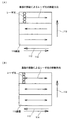
次に、このようなレーザ光を基板の全面に照射する方法について、図3を用いて説明する。
【0041】
レーザ光に対して基板110(または図1のステージ111)を112で示す方向に移動し、続いて113で示す方向へ移動する。この動作を繰り返すことで、基板110の全面を照射することができる。(図3(A))また、レーザ光に対して基板110(または図1のステージ111)を112で示す方向に移動し、さらに114で示す方向に移動させたのち、113で示す方向へ移動させてもよいし、レーザ光に対して基板110(または図1のステージ111)を112で示す方向に移動し、さらに114で示す方向に移動させる動作を複数回繰り返した後、113で示す方向へ移動させてもよい。(図3(B))もちろん、レーザ光を移動させることで、基板の全面を照射してもよい。
【0042】
次に、このような照射方法を用いて、半導体膜の結晶化を行う場合について説明する。レーザ光が半導体膜に照射されると、照射された領域は溶融状態になり、時間が経過するにつれ冷却し固化する。レーザ光を移動させながら照射すれば、次々と溶融状態である領域が形成される一方で、時間の経過により冷却し固化する領域も存在する。つまり、半導体膜中において温度勾配が形成され、レーザ光の移動方向に沿って結晶粒が成長し、大粒径の結晶粒が並列に形成される。
【0043】
そして、大粒径の結晶粒が並列に形成されている結晶性半導体膜を得ることにより、半導体装置の性能を大幅に向上させうる。例えば、TFTを例に挙げると、大粒径の結晶粒が並列に形成されることでチャネル形成領域に含まれうる結晶粒界の本数を少なくすることができる。つまり、キャリアが結晶粒界を横切る回数を極端に減らすことができるため、単結晶半導体を用いたトランジスタと同等もしくはそれ以上の高いモビリティ(電界効果移動度)を得ることが可能であり、オン電流値(TFTがオン状態にある時に流れるドレイン電流値)、オフ電流値(TFTがオフ状態にある時に流れるドレイン電流値)、しきい値電圧、S値及び電界効果移動度のバラツキを低減することも可能となる。このように、TFTの電気的特性は向上し、さらには半導体装置の動作特性および信頼性をも向上し得る。なお、レーザ光の移動方向には結晶粒界がほとんどないため、この方向に平行なチャネル形成領域を有するTFTを作製することが好ましい。
【0044】
また、半導体膜の全面にレーザ光を照射して結晶粒を形成するため、結晶粒の幅と、複数に分割されたレーザ光により形成される干渉のピッチpとを一致させることが望ましい。レーザ光の波長をλ、入射角をθとすると、図2(A)より、
sinθ=λ/p
∴θ=arcsin(λ/p)
が成り立つ。例えば、YAGレーザやYVO4レーザの第2高調波(波長532nm)を用い、形成される結晶粒の幅が1〜10μmであるとき、
θ=arcsin(532/1000)
=32.14
θ=arcsin(532/10000)
=3.05
より、入射角θは3〜32度となる。
【0045】
なお、形成される結晶粒の幅が10μm以上になると、結晶内に亀裂が入り欠陥が生じる可能性が高くなる。一方、1μm未満では、膜中の結晶粒界が増加してしまい、リーク電流の原因となってしまう。このため、結晶粒の幅は、1〜10μmの範囲が好ましい。
このような照射方法を用いれば、大面積基板においても全面にレーザアニールを行うことができる。また、このようなレーザアニールにより半導体膜の結晶化を行うと、大粒径の結晶粒が並列に存在する半導体膜を形成することが可能となる。このため、結晶粒界が減少し、モビリティ(電界効果移動度)の向上、およびオン電流値(TFTがオン状態にある時に流れるドレイン電流値)、オフ電流値(TFTがオフ状態にある時に流れるドレイン電流値)、しきい値電圧、S値及び電界効果移動度のバラツキを低減することも可能となる。よって前記半導体膜を用いて作製されたTFTの電気的特性は向上し、半導体装置の動作特性および信頼性をも向上し得る。
また、基板表面に対して垂直にレーザ光を入射させると、基板裏面から反射されるレーザ光と照射されるレーザ光とが基板表面で干渉を起し、エネルギー密度の分布が不均一となり、結晶性が不均一な半導体膜が形成されるという問題があるが、レーザ光を基板に対して斜めに照射することにより、この問題が解決され、均一な結晶性の半導体膜を形成することができる。
【0046】
以上の構成でなる本発明について、以下に示す実施例によりさらに詳細な説明を行うこととする。
【0047】
【実施例】
[実施例1]
本実施例では、基板の全面にレーザ光を照射するための方法および装置について図1を用いて説明する。
【0048】
レーザ101から射出したレーザ光は、非線形光学素子102により高調波に変換するのが望ましい。本実施例では、レーザ101として連続発振のYAGレーザを用い、非線形光学素子102により第2高調波に変換する。
【0049】
そして、レーザ光をミラー103に照射することでレーザ光の光路を2方向に分割し、それぞれのレーザ光をミラー104a、104bに入射させる。そして、好ましくはシリンドリカルレンズ105a、105bにより、レーザ光の一方向について長さを縮小する。このようにすることで、エネルギー密度を高めることができる。
【0050】
ミラー104a、104bを反射したレーザ光は照射面である基板110に到達する。すなわち、ミラー104a、104bを反射したレーザ光は、照射面である基板110上で重畳する。図2に示すように、前記基板110上では2方向から到達したレーザ光が干渉を起こし、周期的なエネルギー分布が生じる。これは点状のレーザ光が多数並べられていると見なすことができ、点状のレーザ光が1つである場合よりも効率良くレーザ光の照射を行うことができる。
【0051】
また、図示しないが、それぞれの反射光がお互いの入射に至る光路をたどって、レーザに悪影響を及ぼす可能性があるため、アイソレータを設置するのが望ましい。
【0052】
このようなレーザ光に対して基板100(または図1のステージ111)を112で示す方向に移動し、続いて113で示す方向へ移動する。この動作を繰り返すことで、基板の全面を照射することができる。(図3(A))また、レーザ光に対して基板100(または図1のステージ111)を112で示す方向に移動し、さらに114で示す方向に移動させたのち、113で示す方向へ移動させてもよいし、レーザ光に対して基板100(または図1のステージ111)を112で示す方向に移動し、さらに114で示す方向に移動させる動作を複数回繰り返した後、113で示す方向へ移動させてもよい。(図3(B))もちろん、レーザ光を移動させることで、基板の全面を照射してもよい。
【0053】
このようにして、効率よく、基板の全面にレーザ光を照射することできる。この照射方法を用い、半導体膜のアニールや、不純物元素の活性化などを行うことができる。
【0054】
[実施例2]
本実施例では、実施例1とは異なるレーザ光の分割方法により基板の全面にレーザ光を照射するための方法および装置について図4を用いて説明する。
【0055】
レーザ101から射出したレーザ光は、非線形光学素子102により高調波に変換するのが望ましい。本実施例では、レーザ101として、連続発振のYVO4レーザを用い、非線形光学素子102により第3高調波に変換する。
【0056】
そして、レーザ光をプリズム121に照射することで、レーザ光の光路を2方向に分割し、それぞれのレーザ光をミラー122a、122bに入射させる。そして、好ましくはシリンドリカルレンズ105a、105bにより、レーザ光の一方向の長さを縮小する。このようにすることで、エネルギー密度を高めることができる。
【0057】
続いて、レーザ光は照射面である基板110に到達する。すなわち、ミラー122a、122bを反射したレーザ光は、照射面である基板110上で重畳する。これにより、図2に示すように、前記基板110上では2方向から到達したレーザ光が干渉を起こし、周期的なエネルギー分布が生じている。この様子は点状のレーザ光が多数並べられていると見なすことができ、点状のレーザ光が1つである場合よりも効率良くレーザ光の照射を行うことができる。
【0058】
また、基板の移動方法については実施例1と同様である。
【0059】
このようにして、効率よく、基板の全面にレーザ光を照射することができる。
この照射方法を用い、半導体膜のアニールや、不純物元素の活性化などを行うことができる。
【0060】
[実施例3]
本実施例では、実施例1および実施例2とは異なる方法でレーザ光を分割し、基板の全面にレーザ光を照射するための方法および装置について図5を用いて説明する。
【0061】
レーザ101から射出したレーザ光は、非線形光学素子102により高調波に変換するのが望ましい。本実施例では、レーザ101としてYLFレーザを用い、非線形光学素子102により第3高調波に変換する。
【0062】
そして、レーザ光をシリンドリカルレンズアレイ131に入射することで分割する。本実施例では分割数を4としている。続いて、シリンドリカルレンズ132により、レーザ光の集光および発散を行う。これにより4分割されたそれぞれのレーザ光の進行方向(すなわち、レーザ光の光路)を互いに異なるようにすることができるため、それぞれのレーザ光を異なる光学素子に入射させることが容易となる。そして、分割したレーザ光をレンズ133a〜133cに入射させる。レンズ133a、133cは、レンズ133bに対して非対称に設置することで(具体的には、レンズ133bの側面およびレンズ133aの距離(X)と、レンズ133bの側面およびレンズ133cの距離(Y)とが異なるように配置する)、照射面において、133a、133cを透過したレーザ光による干渉と、133bを透過した2つのレーザ光による干渉とのエネルギー分布をずらすことができる。また、対称的に設置すれば、照射面におけるレーザ光のエネルギー分布の高低差を大きくすることもできる。なお、レンズ133a、133cはマイクロメータ等を用いて可動式とすれば、微調整が可能となるので望ましい。
【0063】
レンズ133a、133cを透過した2つのレーザ光は、レーザ101から射出したレーザ光の両端の部分であるため、レンズ133bを透過したレーザ光よりエネルギー密度は低い。そこで、レンズ133a、133cを透過したレーザ光による干渉と、レンズ133bを透過した2つのレーザ光による干渉とのエネルギー分布を、例えば半周期ずらして重ねることで、照射面において極端にエネルギー密度の低い部分が発生するのを防ぐことができる。(図6)もちろん、それぞれのレーザ光のエネルギー密度を同じにし、レンズ133a、133cを透過したレーザ光による干渉と、133bを透過した2つのレーザ光による干渉とのエネルギー分布を半周期ずらして重ねれば、エネルギー分布が均一なレーザ光を作ることも可能である。(図7)
【0064】
また、レンズ133a〜133cと基板110の間にシリンドリカルレンズを設置しても良い。
【0065】
なお、基板の移動方法については実施例1と同様である。
【0066】
このようにして、効率よく、基板の全面にレーザ光を照射することできる。この照射方法を用い、半導体膜のアニールや、不純物元素の活性化などを行うことができる。
【0067】
また、本実施例では、シリンドリカルレンズ132によりレーザ光を集光させ発散させた後、さらにレンズ133を用いて集光させているが、132によって複数のレーザ光を干渉させることもできる。
【0068】
[実施例4]
本実施例では、実施例1乃至実施例3とは異なる方法でレーザ光を分割し、基板の全面にレーザ光を照射するための方法および装置について図8を用いて説明する。
【0069】
レーザ101から射出したレーザ光は、非線形光学素子102により高調波に変換するのが望ましい。レーザ101としては、連続発振またはパルス発振のYAGレーザ、YVO4レーザ、YLFレーザ、YAlO3レーザ、ガラスレーザ、ルビーレーザ、アレキサンドライドレーザ、Ti:サファイアレーザなどを用いることができる。本実施例では、YLFレーザを用い、第2高調波に変換する。
【0070】
そして、レーザ光をプリズム141に照射することで分割する。本実施例では分割数を4としている。プリズム141は、実施例3にて示したシリンドリカルレンズアレイ131とシリンドリカルレンズ132の組み合わせと同様の役割を持つ。プリズム141を使うことで、光学素子の数を2から1に減らすことができるため、光学透過率を向上させることができる。また、光路長が実施例3にて示した系よりも短くてよいという効果もある。短い光路にすることは、単位面積当たりのコストが非常に高いクリーンルームに設置する場合に特に有効である。
そして、分割したレーザ光をレンズ133a〜133cに入射させる。レンズ133a、133cは、レンズ133bに対して非対称に設置することで、即ち、レンズ133aおよび133bの距離とレンズ133cおよび133bの距離とが異なる位置に、それぞれのレンズを設置することで、照射面において、133a、133cを透過したレーザ光による干渉と、133bを透過した2つのレーザ光による干渉とをずらすことができる。また、対称的に設置すれば、照射面におけるレーザ光のエネルギー分布の高低差を大きくすることもできる。なお、レンズ133a、133cはマイクロメータ等を用いて可動式とすれば、微調整が可能となるので望ましい。
【0071】
レンズ133a、133cを透過した2つのレーザ光は、レーザ101から射出したレーザ光の両端の部分であるため、レンズ133bを透過したレーザ光よりエネルギー密度は低い。そこで、レンズ133a、133cを透過したレーザ光による干渉と、レンズ133bを透過した2つのレーザ光による干渉とを、例えば半周期ずらして重ねることで、照射面において極端にエネルギー密度の低い部分が発生するのを防ぐことができる。(図6)もちろん、それぞれのレーザ光のエネルギー密度を同じにし、レンズ133a、133cを透過したレーザ光による干渉と、レンズ133bを透過した2つのレーザ光による干渉とを半周期ずらして重ねれば、エネルギー密度が均一なレーザ光を作ることも可能である。(図7)
【0072】
また、レンズ133a〜133cと基板110の間にシリンドリカルレンズを設置しても良い。
【0073】
なお、基板の移動方法については実施例1と同様である。
【0074】
このようにして、効率よく、基板の全面に照射することできる。この照射方法を用い、半導体膜のアニールや、不純物元素の活性化などを行うことができる。
【0075】
[実施例5]
本実施例ではアクティブマトリクス基板の作製方法について図9〜図12を用いて説明する。本明細書ではCMOS回路、及び駆動回路と、画素TFT、保持容量とを有する画素部を同一基板上に形成された基板を、便宜上アクティブマトリクス基板と呼ぶ。
【0076】
まず、本実施例ではバリウムホウケイ酸ガラス、またはアルミノホウケイ酸ガラスなどのガラスからなる基板400を用いる。なお、基板400としては、石英基板やシリコン基板、金属基板またはステンレス基板の表面に絶縁膜を形成したものを用いても良い。また、本実施例の処理温度に耐えうる耐熱性が有するプラスチック基板を用いてもよい。
【0077】
次いで、基板400上に酸化珪素膜、窒化珪素膜または酸化窒化珪素膜などの絶縁膜から成る下地膜401を公知の手段(スパッタ法、LPCVD法、プラズマCVD法等)により形成する。本実施例では下地膜401として2層構造を用いるが、前記絶縁膜の単層膜または2層以上積層させた構造を用いても良い。
【0078】
次いで、下地膜上に半導体層を形成する。半導体層は公知の手段(スパッタ法、LPCVD法、プラズマCVD法等)により25〜80nm(好ましくは30〜60nm)の厚さで半導体膜を成膜し、レーザ結晶化法により結晶化させる。
レーザ結晶化法は、実施例1乃至4のいずれか一を適用して、レーザから射出されたレーザ光を光学系により複数のレーザ光に分割したのち1つに合成して干渉を形成し、半導体膜に照射する。もちろん、レーザ結晶化法だけでなく、他の公知の結晶化法(RTAやファーネスアニール炉を用いた熱結晶化法、結晶化を助長する金属元素を用いた熱結晶化法等)と組み合わせて行ってもよい。そして、得られた結晶性半導体膜を所望の形状にパターニングして半導体層402〜406を形成する。前記半導体膜としては、非晶質半導体膜や微結晶半導体膜、結晶性半導体膜などがあり、非晶質珪素ゲルマニウム膜などの非晶質構造を有する化合物半導体膜を適用しても良い。
【0079】
本実施例では、まず、プラズマCVD法を用い、55nmの非晶質珪素膜を成膜する。そして、出力10Wの連続発振のYVO4レーザから射出されたレーザ光を非線形光学素子により第2高調波に変換したのち、実施例1乃至4のいずれか一に示す光学系より複数のレーザ光に分割し、基板上にて合成して干渉を形成する。このときのエネルギー密度の分布は波状となるが、結晶化にはピーク値が150mJ/cm2以上(好ましくは200mJ/cm2以上)のエネルギー密度を有するレーザ光が必要である。そして、10〜200cm/s程度の速度でステージを動かして照射し、結晶性珪素膜を形成する。続いて、フォトリソグラフィ法を用いたパターニング処理によって半導体層402〜406を形成する。
【0080】
また、半導体層402〜406を形成した後、TFTのしきい値を制御するために微量な不純物元素(ボロンまたはリン)のドーピングを行ってもよい。
【0081】
次いで、半導体層402〜406を覆うゲート絶縁膜407を形成する。ゲート絶縁膜407はプラズマCVD法またはスパッタ法を用い、厚さを40〜150nmとして珪素を含む絶縁膜で形成する。本実施例では、プラズマCVD法により110nmの厚さで酸化窒化珪素膜(組成比Si=32%、O=59%、N=7%、H=2%)で形成した。勿論、ゲート絶縁膜は酸化窒化珪素膜に限定されるものでなく、他の珪素を含む絶縁膜を単層または積層構造として用いても良い。
【0082】
また、酸化珪素膜を用いる場合には、プラズマCVD法でTEOS(Tetraethyl Orthosilicate)とO2とを混合し、反応圧力40Pa、基板温度300〜400℃とし、高周波(13.56MHz)電力密度0.5〜0.8W/cm2で放電させて形成することができる。このようにして作製される酸化珪素膜は、その後400〜500℃の熱アニールによりゲート絶縁膜として良好な特性を得ることができる。
【0083】
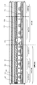
次いで、ゲート絶縁膜407上に膜厚20〜100nmの第1の導電膜408と、膜厚100〜400nmの第2の導電膜409とを積層形成する。本実施例では、膜厚30nmのTaN膜からなる第1の導電膜408と、膜厚370nmのW膜からなる第2の導電膜409を積層形成した。TaN膜はスパッタ法で形成し、Taのターゲットを用い、窒素を含む雰囲気内でスパッタする。また、W膜は、Wのターゲットを用いたスパッタ法で形成した。その他に6フッ化タングステン(WF6)を用いる熱CVD法で形成することもできる。いずれにしてもゲート電極として使用するためには低抵抗化を図る必要があり、W膜の抵抗率は20μΩcm以下にすることが望ましい。W膜は結晶粒を大きくすることで低抵抗率化を図ることができるが、W膜中に酸素などの不純物元素が多い場合には結晶化が阻害され高抵抗化する。従って、本実施例では、高純度のW(純度99.9999%)のターゲットを用いたスパッタ法で、さらに成膜時に気相中からの不純物の混入がないように十分配慮してW膜を形成することにより、抵抗率9〜20μΩcmを実現することができる。
【0084】
なお、本実施例では、第1の導電膜408をTaN、第2の導電膜409をWとしたが、特に限定されず、いずれもTa、W、Ti、Mo、Al、Cu、Cr、Ndから選ばれた元素、または前記元素を主成分とする合金材料若しくは化合物材料で形成してもよい。また、リン等の不純物元素をドーピングした多結晶珪素膜に代表される半導体膜を用いてもよい。また、AgPdCu合金を用いてもよい。また、第1の導電膜をタンタル(Ta)膜で形成し、第2の導電膜をW膜とする組み合わせ、第1の導電膜を窒化チタン(TiN)膜で形成し、第2の導電膜をW膜とする組み合わせ、第1の導電膜を窒化タンタル(TaN)膜で形成し、第2の導電膜をAl膜とする組み合わせ、第1の導電膜を窒化タンタル(TaN)膜で形成し、第2の導電膜をCu膜とする組み合わせとしてもよい。
【0085】
次に、フォトリソグラフィ法を用いてレジストからなるマスク410〜415を形成し、電極及び配線を形成するための第1のエッチング処理を行う。第1のエッチング処理では第1及び第2のエッチング条件で行う。(図9(B))本実施例では第1のエッチング条件として、ICP(Inductively Coupled Plasma:誘導結合型プラズマ)エッチング法を用い、エッチング用ガスにCF4とCl2とO2とを用い、それぞれのガス流量比を25:25:10(sccm)とし、1Paの圧力でコイル型の電極に500WのRF(13.56MHz)電力を投入してプラズマを生成してエッチングを行う。基板側(試料ステージ)にも150WのRF(13.56MHz)電力を投入し、実質的に負の自己バイアス電圧を印加する。この第1のエッチング条件によりW膜をエッチングして第1の導電層の端部をテーパー形状とする。
【0086】
この後、レジストからなるマスク410〜415を除去せずに第2のエッチング条件に変え、エッチング用ガスにCF4とCl2とを用い、それぞれのガス流量比を30:30(sccm)とし、1Paの圧力でコイル型の電極に500WのRF(13.56MHz)電力を投入してプラズマを生成して約30秒程度のエッチングを行った。基板側(試料ステージ)にも20WのRF(13.56MHz)電力を投入し、実質的に負の自己バイアス電圧を印加する。CF4とCl2を混合した第2のエッチング条件ではW膜及びTaN膜とも同程度にエッチングされる。なお、ゲート絶縁膜上に残渣を残すことなくエッチングするためには、10〜20%程度の割合でエッチング時間を増加させると良い。
【0087】
上記第1のエッチング処理では、レジストからなるマスクの形状を適したものとすることにより、基板側に印加するバイアス電圧の効果により第1の導電層及び第2の導電層の端部がテーパー形状となる。このテーパー部の角度は15〜45°となる。こうして、第1のエッチング処理により第1の導電層と第2の導電層から成る第1の形状の導電層417〜422(第1の導電層417a〜422aと第2の導電層417b〜422b)を形成する。416はゲート絶縁膜であり、第1の形状の導電層417〜422で覆われない領域は20〜50nm程度エッチングされ薄くなった領域が形成される。
【0088】
次いで、レジストからなるマスクを除去せずに第2のエッチング処理を行う。
(図9(C))ここでは、エッチングガスにCF4とCl2とO2とを用い、W膜を選択的にエッチングする。この時、第2のエッチング処理により第2の導電層428b〜433bを形成する。一方、第1の導電層417a〜422aは、ほとんどエッチングされず、第2の形状の導電層428〜433を形成する。
【0089】
そして、レジストからなるマスクを除去せずに第1のドーピング処理を行い、半導体層にn型を付与する不純物元素を低濃度に添加する。ドーピング処理はイオンドープ法、若しくはイオン注入法で行えば良い。イオンドープ法の条件はドーズ量を1×10¹³〜5×10¹⁴/cm2とし、加速電圧を40〜80keVとして行う。本実施例ではドーズ量を1.5×1013/cm2とし、加速電圧を60keVとして行う。n型を付与する不純物元素として15族に属する元素、典型的にはリン(P)または砒素(As)を用いるが、ここではリン(P)を用いる。この場合、導電層428〜433がn型を付与する不純物元素に対するマスクとなり、自己整合的に不純物領域423〜427が形成される。不純物領域423〜427には1×1018〜1×1020/cm3の濃度範囲でn型を付与する不純物元素を添加する。
【0090】
レジストからなるマスクを除去した後、新たにレジストからなるマスク434a〜434cを形成して第1のドーピング処理よりも高い加速電圧で第2のドーピング処理を行う。イオンドープ法の条件はドーズ量を1×10¹³〜1×10¹⁵/cm2とし、加速電圧を60〜120keVとして行う。ドーピング処理は第2の導電層428b〜432bを不純物元素に対するマスクとして用い、第1の導電層のテーパー部の下方の半導体層に不純物元素が添加されるようにドーピングする。続いて、第2のドーピング処理より加速電圧を下げて第3のドーピング処理を行って図10(A)の状態を得る。イオンドープ法の条件はドーズ量を1×1015〜1×1017/cm2とし、加速電圧を50〜100keVとして行う。第2のドーピング処理および第3のドーピング処理により、第1の導電層と重なる低濃度不純物領域436、442、448には1×1018〜5×1019/cm3の濃度範囲でn型を付与する不純物元素を添加され、高濃度不純物領域435、441、444、447には1×1019〜5×1021/cm3の濃度範囲でn型を付与する不純物元素を添加される。
【0091】
もちろん、適当な加速電圧にすることで、第2のドーピング処理および第3のドーピング処理は1回のドーピング処理で、低濃度不純物領域および高濃度不純物領域を形成することも可能である。
【0092】
次いで、レジストからなるマスクを除去した後、新たにレジストからなるマスク450a〜450cを形成して第4のドーピング処理を行う。この第4のドーピング処理により、pチャネル型TFTの活性層となる半導体層に前記一導電型とは逆の導電型を付与する不純物元素が添加された不純物領域453、454、459、460を形成する。第2の導電層428a〜432aを不純物元素に対するマスクとして用い、p型を付与する不純物元素を添加して自己整合的に不純物領域を形成する。本実施例では、不純物領域453、454、459、460はジボラン(B2H6)を用いたイオンドープ法で形成する。(図10(B))この第4のドーピング処理の際には、nチャネル型TFTを形成する半導体層はレジストからなるマスク450a〜450cで覆われている。第1乃至3のドーピング処理によって、不純物領域453、459にはそれぞれ異なる濃度でリンが添加されているが、そのいずれの領域においてもp型を付与する不純物元素の濃度を1×10¹⁹〜5×10²¹atoms/cm3となるようにドーピング処理することにより、pチャネル型TFTのソース領域およびドレイン領域として機能するために何ら問題は生じない。
【0093】
以上までの工程で、それぞれの半導体層に不純物領域が形成される。
【0094】
次いで、レジストからなるマスク450a〜450cを除去して第1の層間絶縁膜461を形成する。この第1の層間絶縁膜461としては、プラズマCVD法またはスパッタ法を用い、厚さを100〜200nmとして珪素を含む絶縁膜で形成する。本実施例では、プラズマCVD法により膜厚150nmの酸化窒化珪素膜を形成した。勿論、第1の層間絶縁膜461は酸化窒化珪素膜に限定されるものでなく、他の珪素を含む絶縁膜を単層または積層構造として用いても良い。
【0095】
次いで、図10(C)に示すように、活性化処理としてレーザ照射方法を用いる。レーザ照射方法では、実施例1乃至4のいずれか一を適用してレーザから射出されたレーザ光を光学系により複数のレーザ光に分割したのち1つに合成して干渉を形成し、半導体膜に照射する。
【0096】
本実施例では、出力10Wの連続発振のYVO4レーザから射出されたレーザ光を非線形光学素子により第3高調波に変換したのち、実施例1乃至4のいずれか一に示す光学系を用いて複数のレーザ光に分割し、基板上にて合成して干渉を形成する。このときのエネルギー密度の分布は波状となるが、結晶化にはピーク値が80mJ/cm2以上(好ましくは100mJ/cm2以上)のエネルギー密度であるレーザ光が必要である。そして、10〜200cm/s程度の速度でステージを動かして照射する。
【0097】
また、第1の層間絶縁膜を形成する前に活性化処理を行っても良い。
【0098】
そして、加熱処理(300〜550℃で1〜12時間の熱処理)を行うと水素化を行うことができる。この工程は第1の層間絶縁膜461に含まれる水素により半導体層のダングリングボンドを終端する工程である。第1の層間絶縁膜の存在に関係なく半導体層を水素化することができる。水素化の他の手段として、プラズマ水素化(プラズマにより励起された水素を用いる)や、3〜100%の水素を含む雰囲気中で300〜450℃で1〜12時間の加熱処理を行っても良い。
【0099】
次いで、第1の層間絶縁膜461上に無機絶縁膜材料または有機絶縁物材料から成る第2の層間絶縁膜462を形成する。本実施例では、膜厚1.6μmのアクリル樹脂膜を形成したが、粘度が10〜1000cp、好ましくは40〜200cpのものを用い、表面に凸凹が形成されるものを用いる。
【0100】
本実施例では、鏡面反射を防ぐため、表面に凸凹が形成される第2の層間絶縁膜を形成することによって画素電極の表面に凸凹を形成した。また、画素電極の表面に凹凸を持たせて光散乱性を図るため、画素電極の下方の領域に凸部を形成してもよい。その場合、凸部の形成は、TFTの形成と同じフォトマスクで行うことができるため、工程数の増加なく形成することができる。なお、この凸部は配線及びTFT部以外の画素部領域の基板上に適宜設ければよい。こうして、凸部を覆う絶縁膜の表面に形成された凸凹に沿って画素電極の表面に凸凹が形成される。
【0101】
また、第2の層間絶縁膜462として表面が平坦化する膜を用いてもよい。その場合は、画素電極を形成した後、公知のサンドブラスト法やエッチング法等の工程を追加して表面を凹凸化させて、鏡面反射を防ぎ、反射光を散乱させることによって白色度を増加させることが好ましい。
【0102】
そして、駆動回路506において、各不純物領域とそれぞれ電気的に接続する配線463〜467を形成する。なお、これらの配線は、膜厚50nmのTi膜と、膜厚500nmの合金膜(AlとTiとの合金膜)との積層膜をパターニングして形成する。もちろん、二層構造に限らず、単層構造でもよいし、三層以上の積層構造にしてもよい。また、配線の材料としては、AlとTiに限らない。
例えば、TaN膜上にAlやCuを形成し、さらにTi膜を形成した積層膜をパターニングして配線を形成してもよい。(図11)
【0103】
また、画素部507においては、画素電極470、ゲート配線469、接続電極468を形成する。この接続電極468によりソース配線(443aと443bの積層)は、画素TFTと電気的な接続が形成される。また、ゲート配線469は、画素TFTのゲート電極と電気的な接続が形成される。また、画素電極470は、画素TFTのドレイン領域と電気的な接続が形成され、さらに保持容量を形成する一方の電極として機能する半導体層459と電気的な接続が形成される。また、画素電極470としては、AlまたはAgを主成分とする膜、またはそれらの積層膜等の反射性の優れた材料を用いることが望ましい。
【0104】
以上の様にして、nチャネル型TFT501とpチャネル型TFT502からなるCMOS回路、及びnチャネル型TFT503を有する駆動回路506と、画素TFT504、保持容量505とを有する画素部507を同一基板上に形成することができる。こうして、アクティブマトリクス基板が完成する。
【0105】
駆動回路506のnチャネル型TFT501はチャネル形成領域437、ゲート電極の一部を構成する第1の導電層428aと重なる低濃度不純物領域436(GOLD領域)、ソース領域またはドレイン領域として機能する高濃度不純物領域452と、n型を付与する不純物元素およびp型を付与する不純物元素が導入された不純物領域451を有している。このnチャネル型TFT501と電極466で接続してCMOS回路を形成するpチャネル型TFT502にはチャネル形成領域440、ソース領域またはドレイン領域として機能する高濃度不純物領域454と、n型を付与する不純物元素およびp型を付与する不純物元素が導入された不純物領域453を有している。また、nチャネル型TFT503にはチャネル形成領域443、ゲート電極の一部を構成する第1の導電層430aと重なる低濃度不純物領域442(GOLD領域)、ソース領域またはドレイン領域として機能する高濃度不純物領域456と、n型を付与する不純物元素およびp型を付与する不純物元素が導入された不純物領域455を有している。
【0106】
画素部の画素TFT504にはチャネル形成領域446、ゲート電極の外側に形成される低濃度不純物領域445(LDD領域)、ソース領域またはドレイン領域として機能する高濃度不純物領域458とを有している。また、保持容量505の一方の電極として機能する半導体層には、n型を付与する不純物元素およびp型を付与する不純物元素が添加されている。保持容量505は、絶縁膜416を誘電体として、電極(432aと432bの積層)と、半導体層とで形成している。
【0107】
本実施例の画素構造は、ブラックマトリクスを用いることなく、画素電極間の隙間が遮光されるように、画素電極の端部をソース配線と重なるように配置形成する。
【0108】
また、本実施例で作製するアクティブマトリクス基板の画素部の上面図を図12に示す。なお、図9〜図12に対応する部分には同じ符号を用いている。図11中の鎖線A−A’は図12中の鎖線A―A’で切断した断面図に対応している。また、図11中の鎖線B−B’は図12中の鎖線B―B’で切断した断面図に対応している。
【0109】
[実施例6]
本実施例では、実施例5で作製したアクティブマトリクス基板から、反射型液晶表示装置を作製する工程を以下に説明する。説明には図13を用いる。
【0110】
まず、実施例5に従い、図11の状態のアクティブマトリクス基板を得た後、図11のアクティブマトリクス基板上、少なくとも画素電極470上に配向膜567を形成しラビング処理を行う。なお、本実施例では配向膜567を形成する前に、アクリル樹脂膜等の有機樹脂膜をパターニングすることによって基板間隔を保持するための柱状のスペーサ572を所望の位置に形成した。また、柱状のスペーサに代えて、球状のスペーサを基板全面に散布してもよい。
【0111】
次いで、対向基板569を用意する。次いで、対向基板569上に着色層570、571、平坦化膜573を形成する。赤色の着色層570と青色の着色層571とを重ねて、遮光部を形成する。また、赤色の着色層と緑色の着色層とを一部重ねて、遮光部を形成してもよい。
【0112】
本実施例では、実施例5に示す基板を用いている。従って、実施例5の画素部の上面図を示す図12では、少なくともゲート配線469と画素電極470の間隙と、ゲート配線469と接続電極468の間隙と、接続電極468と画素電極470の間隙を遮光する必要がある。本実施例では、それらの遮光すべき位置に着色層の積層からなる遮光部が重なるように各着色層を配置して、対向基板を貼り合わせた。
【0113】
このように、ブラックマスク等の遮光層を形成することなく、各画素間の隙間を着色層の積層からなる遮光部で遮光することによって工程数の低減を可能とした。
【0114】
次いで、平坦化膜573上に透明導電膜からなる対向電極576を少なくとも画素部に形成し、対向基板の全面に配向膜574を形成し、ラビング処理を施した。
【0115】
そして、画素部と駆動回路が形成されたアクティブマトリクス基板と対向基板とをシール材568で貼り合わせる。シール材568にはフィラーが混入されていて、このフィラーと柱状スペーサによって均一な間隔を持って2枚の基板が貼り合わせられる。その後、両基板の間に液晶材料575を注入し、封止剤(図示せず)によって完全に封止する。液晶材料575には公知の液晶材料を用いれば良い。このようにして図13に示す反射型液晶表示装置が完成する。そして、必要があれば、アクティブマトリクス基板または対向基板を所望の形状に分断する。さらに、対向基板のみに偏光板(図示しない)を貼りつけた。そして、公知の技術を用いてFPCを貼りつけた。
【0116】
以上のようにして作製される液晶表示装置はエネルギー分布が周期的または一様なレーザ光が照射され、大粒径の結晶粒が形成された半導体膜を用いて作製されたTFTを有しており、前記液晶表示装置の動作特性や信頼性を十分なものとなり得る。そして、このような液晶表示装置は各種電子機器の表示部として用いることができる。
【0117】
なお、本実施例は実施例1乃至5と自由に組み合わせることが可能である。
【0118】
[実施例7]
本実施例では、実施例5で示したアクティブマトリクス基板を作製するときのTFTの作製方法を用いて、発光装置を作製する例を以下に説明する。本明細書において、発光装置とは、基板上に形成された発光素子を該基板とカバー材の間に封入した表示用パネルおよび該表示用パネルにTFT等を実装した表示用モジュールを総称したものである。なお、発光素子は、電場を加えることで発生するルミネッセンス(Electro Luminescence)が得られる化合物を含む層(発光体)と陽極層と、陰極層とを有する。また、化合物におけるルミネッセンスには、一重項励起状態から基底状態に戻る際の発光(蛍光)と三重項励起状態から基底状態に戻る際の発光(リン光)があり、これらのうちどちらか、あるいは両方の発光を含む。
【0119】
なお、本明細書中では、発光素子において陽極と陰極の間に形成された全ての層を発光体と定義する。発光体には具体的に、発光層、正孔注入層、電子注入層、正孔輸送層、電子輸送層等が含まれる。基本的に発光素子は、陽極層、発光体、陰極層が順に積層された構造を有しており、この構造に加えて、陽極層、正孔注入層、発光層、陰極層や、陽極層、正孔注入層、発光層、電子輸送層、陰極層等の順に積層した構造を有していることもある。
【0120】
図14は本実施例の発光装置の断面図である。図14において、基板700上に設けられたスイッチングTFT603は図11のnチャネル型TFT503を用いて形成される。したがって、構造の説明はnチャネル型TFT503の説明を参照すれば良い。
【0121】
なお、本実施例ではチャネル形成領域が二つ形成されるダブルゲート構造としているが、チャネル形成領域が一つ形成されるシングルゲート構造もしくは三つ形成されるトリプルゲート構造であっても良い。
【0122】
基板700上に設けられた駆動回路は図11のCMOS回路を用いて形成される。従って、構造の説明はnチャネル型TFT501とpチャネル型TFT502の説明を参照すれば良い。なお、本実施例ではシングルゲート構造としているが、ダブルゲート構造もしくはトリプルゲート構造であっても良い。
【0123】
また、配線701、703はCMOS回路のソース配線、702はドレイン配線として機能する。また、配線704はソース配線とスイッチングTFTのソース領域とを電気的に接続する配線として機能し、配線705はドレイン配線とスイッチングTFTのドレイン領域とを電気的に接続する配線として機能する。
【0124】
なお、電流制御TFT604は図11のpチャネル型TFT502を用いて形成される。従って、構造の説明はpチャネル型TFT502の説明を参照すれば良い。なお、本実施例ではシングルゲート構造としているが、ダブルゲート構造もしくはトリプルゲート構造であっても良い。
【0125】
また、配線706は電流制御TFTのソース配線(電流供給線に相当する)であり、707は電流制御TFTの画素電極711上に重ねることで画素電極711と電気的に接続する電極である。
【0126】
なお、711は、透明導電膜からなる画素電極(発光素子の陽極)である。透明導電膜としては、酸化インジウムと酸化スズとの化合物、酸化インジウムと酸化亜鉛との化合物、酸化亜鉛、酸化スズまたは酸化インジウムを用いることができる。また、前記透明導電膜にガリウムを添加したものを用いても良い。画素電極711は、上記配線を形成する前に平坦な層間絶縁膜710上に形成する。本実施例においては、樹脂からなる平坦化膜710を用いてTFTによる段差を平坦化することは非常に重要である。後に形成される発光体は非常に薄いため、段差が存在することによって発光不良を起こす場合がある。従って、発光体をできるだけ平坦面に形成しうるように画素電極を形成する前に平坦化しておくことが望ましい。
【0127】
配線701〜707を形成後、図14に示すようにバンク712を形成する。
バンク712は100〜400nmの珪素を含む絶縁膜もしくは有機樹脂膜をパターニングして形成すれば良い。
【0128】
なお、バンク712は絶縁膜であるため、成膜時における素子の静電破壊には注意が必要である。本実施例ではバンク712の材料となる絶縁膜中にカーボン粒子や金属粒子を添加して抵抗率を下げ、静電気の発生を抑制する。この際、抵抗率は1×10⁶〜1×10¹²Ωm(好ましくは1×10⁸〜1×10¹⁰Ωm)となるようにカーボン粒子や金属粒子の添加量を調節すれば良い。
【0129】
画素電極711の上には発光体713が形成される。なお、図14では一画素しか図示していないが、本実施例ではR(赤)、G(緑)、B(青)の各色に対応した発光層を作り分けている。また、本実施例では蒸着法により低分子系有機発光材料を形成している。具体的には、正孔注入層として20nm厚の銅フタロシアニン(CuPc)膜を設け、その上に発光体として70nm厚のトリス−8−キノリノラトアルミニウム錯体(Alq3)膜を設けた積層構造としている。Alq3にキナクリドン、ペリレンもしくはDCM1といった蛍光色素を添加することで発光色を制御することができる。
【0130】
但し、以上の例は発光体として用いることのできる有機発光材料の一例であって、これに限定する必要はまったくない。発光層、電荷輸送層または電荷注入層を自由に組み合わせて発光体(発光及びそのためのキャリアの移動を行わせるための層)を形成すれば良い。例えば、本実施例では低分子系有機発光材料を発光層として用いる例を示したが、中分子系有機発光材料や高分子系有機発光材料を用いても良い。なお、本明細書中において、昇華性を有さず、かつ、分子数が20以下または連鎖する分子の長さが10μm以下の有機発光材料を中分子系有機発光材料とする。また、高分子系有機発光材料を用いる例として、正孔注入層として20nmのポリチオフェン(PEDOT)膜をスピン塗布法により設け、その上に発光層として100nm程度のパラフェニレンビニレン(PPV)膜を設けた積層構造としても良い。なお、PPVのπ共役系高分子を用いると、赤色から青色まで発光波長を選択できる。また、電荷輸送層や電荷注入層として炭化珪素等の無機材料を用いることも可能である。これらの有機発光材料や無機材料は公知の材料を用いることができる。
【0131】
次に、発光層713の上には導電膜からなる陰極714が設けられる。本実施例の場合、導電膜としてアルミニウムとリチウムとの合金膜を用いる。勿論、公知のMgAg膜(マグネシウムと銀との合金膜)を用いても良い。陰極材料としては、周期表の1族もしくは2族に属する元素からなる導電膜もしくはそれらの元素を添加した導電膜を用いれば良い。
【0132】
この陰極714まで形成された時点で発光素子715が完成する。なお、ここでいう発光素子715は、画素電極(陽極)711、発光層713及び陰極714で形成されたダイオードを指す。
【0133】
発光素子715を完全に覆うようにしてパッシベーション膜716を設けることは有効である。パッシベーション膜716としては、炭素膜、窒化珪素膜もしくは窒化酸化珪素膜を含む絶縁膜からなり、該絶縁膜を単層もしくは組み合わせた積層で用いる。
【0134】
この際、カバレッジの良い膜をパッシベーション膜として用いることが好ましく、炭素膜、特にDLC(ダイヤモンドライクカーボン)膜を用いることは有効である。DLC膜は室温から100℃以下の温度範囲で成膜可能であるため、耐熱性の低い発光体713の上方にも容易に成膜することができる。また、DLC膜は酸素に対するブロッキング効果が高く、発光層713の酸化を抑制することが可能である。そのため、この後に続く封止工程を行う間に発光体713が酸化するといった問題を防止できる。
【0135】
さらに、パッシベーション膜716上に封止材717を設け、カバー材718を貼り合わせる。封止材717としては紫外線硬化樹脂を用いれば良く、内部に吸湿効果を有する物質もしくは酸化防止効果を有する物質を設けることは有効である。また、本実施例においてカバー材718はガラス基板や石英基板やプラスチック基板(プラスチックフィルムも含む)の両面に炭素膜(好ましくはダイヤモンドライクカーボン膜)を形成したものを用いる。
【0136】
こうして図14に示すような構造の発光装置が完成する。なお、バンク712を形成した後、パッシベーション膜716を形成するまでの工程をマルチチャンバー方式(またはインライン方式)の成膜装置を用いて、大気解放せずに連続的に処理することは有効である。また、さらに発展させてカバー材718を貼り合わせる工程までを大気解放せずに連続的に処理することも可能である。
【0137】
こうして、基板700上にnチャネル型TFT601、602、スイッチングTFT(nチャネル型TFT)603および電流制御TFT(nチャネル型TFT)604が形成される。
【0138】
さらに、図14を用いて説明したように、ゲート電極に絶縁膜を介して重なる不純物領域を設けることによりホットキャリア効果に起因する劣化に強いnチャネル型TFTを形成することができる。そのため、信頼性の高い発光装置を実現できる。
【0139】
また、本実施例では画素部と駆動回路の構成のみ示しているが、本実施例の製造工程に従えば、その他にも信号分割回路、D/Aコンバータ、オペアンプ、γ補正回路などの論理回路を同一の絶縁体上に形成可能であり、さらにはメモリやマイクロプロセッサをも形成しうる。
【0140】
以上のようにして作製される発光装置はエネルギー分布が周期的または一様なレーザ光が照射され、大粒径の結晶粒が形成された半導体膜を用いて作製されたTFTを有しており、前記発光装置の動作特性や信頼性を十分なものとなり得る。そして、このような発光装置は各種電子機器の表示部として用いることができる。
【0141】
なお、本実施例は実施例1乃至5のいずれか一と自由に組み合わせることが可能である。
【0142】
[実施例8]
本発明を適用して、様々な半導体装置(アクティブマトリクス型液晶表示装置、アクティブマトリクス型発光装置、アクティブマトリクス型EC表示装置)を作製することができる。即ち、それら電気光学装置を表示部に組み込んだ様々な電子機器に本発明を適用できる。
【0143】
その様な電子機器としては、ビデオカメラ、デジタルカメラ、プロジェクター、ヘッドマウントディスプレイ(ゴーグル型ディスプレイ)、カーナビゲーション、カーステレオ、パーソナルコンピュータ、携帯情報端末(モバイルコンピュータ、携帯電話または電子書籍等)などが挙げられる。それらの例を図15、図16及び図17に示す。
【0144】
図15(A)はパーソナルコンピュータであり、本体3001、画像入力部3002、表示部3003、キーボード3004等を含む。本発明を表示部3003に適用することができる。
【0145】
図15(B)はビデオカメラであり、本体3101、表示部3102、音声入力部3103、操作スイッチ3104、バッテリー3105、受像部3106等を含む。本発明を表示部3102に適用することができる。
【0146】
図15(C)はモバイルコンピュータ(モービルコンピュータ)であり、本体3201、カメラ部3202、受像部3203、操作スイッチ3204、表示部3205等を含む。本発明は表示部3205に適用できる。
【0147】
図15(D)はゴーグル型ディスプレイであり、本体3301、表示部3302、アーム部3303等を含む。本発明は表示部3302に適用することができる。
【0148】
図15(E)はプログラムを記録した記録媒体(以下、記録媒体と呼ぶ)を用いるプレーヤーであり、本体3401、表示部3402、スピーカ部3403、記録媒体3404、操作スイッチ3405等を含む。なお、このプレーヤーは記録媒体としてDVD(Digtial Versatile Disc)、CD等を用い、音楽鑑賞や映画鑑賞やゲームやインターネットを行うことができる。
本発明は表示部3402に適用することができる。
【0149】
図15(F)はデジタルカメラであり、本体3501、表示部3502、接眼部3503、操作スイッチ3504、受像部(図示しない)等を含む。本発明を表示部3502に適用することができる。
【0150】
図16(A)はフロント型プロジェクターであり、投射装置3601、スクリーン3602等を含む。本発明は投射装置3601の一部を構成する液晶表示装置3808やその他の駆動回路に適用することができる。
【0151】
図16(B)はリア型プロジェクターであり、本体3701、投射装置3702、ミラー3703、スクリーン3704等を含む。本発明は投射装置3702の一部を構成する液晶表示装置3808やその他の駆動回路に適用することができる。
【0152】
なお、図16(C)は、図16(A)及び図16(B)中における投射装置3601、3702の構造の一例を示した図である。投射装置3601、3702は、光源光学系3801、ミラー3802、3804〜3806、ダイクロイックミラー3803、プリズム3807、液晶表示装置3808、位相差板3809、投射光学系3810で構成される。投射光学系3810は、投射レンズを含む光学系で構成される。本実施例は三板式の例を示したが、特に限定されず、例えば単板式であってもよい。また、図16(C)中において矢印で示した光路に実施者が適宜、光学レンズや、偏光機能を有するフィルムや、位相差を調節するためのフィルム、IRフィルム等の光学系を設けてもよい。
【0153】
また、図16(D)は、図16(C)中における光源光学系3801の構造の一例を示した図である。本実施例では、光源光学系3801は、リフレクター3811、光源3812、レンズアレイ3813、3814、偏光変換素子3815、集光レンズ3816で構成される。なお、図16(D)に示した光源光学系は一例であって特に限定されない。例えば、光源光学系に実施者が適宜、光学レンズや、偏光機能を有するフィルムや、位相差を調節するフィルム、IRフィルム等の光学系を設けてもよい。
【0154】
ただし、図16に示したプロジェクターにおいては、透過型の電気光学装置を用いた場合を示しており、反射型の電気光学装置及び発光装置での適用例は図示していない。
【0155】
図17(A)は携帯電話であり、本体3901、音声出力部3902、音声入力部3903、表示部3904、操作スイッチ3905、アンテナ3906等を含む。本発明を表示部3904に適用することができる。
【0156】
図17(B)は携帯書籍(電子書籍)であり、本体4001、表示部4002、4003、記憶媒体4004、操作スイッチ4005、アンテナ4006等を含む。本発明は表示部4002、4003に適用することができる。
【0157】
図17(C)はディスプレイであり、本体4101、支持台4102、表示部4103等を含む。本発明は表示部4103に適用することができる。本発明のディスプレイは特に大画面化した場合において有利であり、対角10インチ以上(特に30インチ以上)のディスプレイには有利である。
【0158】
以上の様に、本発明の適用範囲は極めて広く、さまざま分野の電子機器に適用することが可能である。また、本実施例の電子機器は実施例1〜6または7の組み合わせからなる構成を用いても実現することができる。
【0159】
【発明の効果】
本発明の構成を採用することにより、以下に示すような基本的有意性を得ることが出来る。
(a)干渉性の高いエネルギーを有するレーザ光を、半導体膜に適したエネルギー密度を有するレーザ光に成形することができる。
(b)高い干渉性を有するレーザ光にも十分対応し得る。
(c)基板を移動させることで、大面積基板にもレーザ光の照射を行うことが可能となる。
(d)以上の利点を満たした上で、レーザ照射方法およびそれを行うレーザ照射装置において、効率よくレーザ光の照射を行うことができる。また、アクティブマトリクス型の液晶表示装置に代表される半導体装置において、半導体装置の動作特性および信頼性の向上を実現することができる。さらに、半導体装置の製造コストの低減を実現することができる。
【図面の簡単な説明】
【図1】 本発明のレーザ照射装置の構成の例を示す図。
【図2】 本発明の照射面におけるレーザ光の干渉の例を示す図。
【図3】 本発明の照射面における基板の移動方法の例を示す図。
【図4】 本発明のレーザ照射装置の構成の例を示す図。
【図5】 本発明のレーザ照射装置の構成の例を示す図。
【図6】 本発明の照射面におけるレーザ光の干渉の例を示す図。
【図7】 本発明の照射面におけるレーザ光の干渉の例を示す図。
【図8】 本発明の照射面におけるレーザ光の干渉の例を示す図。
【図9】 画素TFT、駆動回路のTFTの作製工程を示す断面図。
【図10】 画素TFT、駆動回路のTFTの作製工程を示す断面図。
【図11】 画素TFT、駆動回路のTFTの作製工程を示す断面図。
【図12】 画素TFTの構成を示す上面図。
【図13】 アクティブマトリクス型液晶表示装置の断面図。
【図14】 発光装置の駆動回路及び画素部の断面構造図。
【図15】 半導体装置の例を示す図。
【図16】 半導体装置の例を示す図。
【図17】 半導体装置の例を示す図。[0001]
BACKGROUND OF THE INVENTION
The present invention relates to a method for irradiating a laser beam (laser beam) and a laser irradiation apparatus for performing the method (an apparatus including a laser and an optical system for guiding a laser beam (laser beam) output from the laser to an object to be processed). About. Further, the present invention relates to a method for manufacturing a semiconductor device manufactured by including laser irradiation in a process. Note that the semiconductor device here includes an electro-optical device such as a liquid crystal display device and a light-emitting device and an electronic device including the electro-optical device as a component.
[0002]
[Prior art]
In recent years, techniques for obtaining a crystalline semiconductor film by performing laser annealing on a semiconductor film formed over an insulating substrate such as glass to crystallize or improve crystallinity have been widely studied. Note that in this specification, a crystalline semiconductor film refers to a semiconductor film in which a crystallized region exists, and includes a semiconductor film in which the entire surface is crystallized.
[0003]
A glass substrate is less expensive than a synthetic quartz glass substrate and has an advantage that a large-area substrate can be easily manufactured. In addition, the reason why lasers are used favorably for crystallization is that the melting point of the glass substrate is low. The laser can give high energy to the semiconductor film without significantly increasing the temperature of the substrate. In addition, the throughput is significantly higher than that of heating means using an electric furnace.
[0004]
Since a crystalline semiconductor film formed by laser light irradiation has high mobility, a thin film transistor (TFT) is formed using the crystalline semiconductor film, for example, on a single glass substrate. Alternatively, it is used in an active matrix type liquid crystal display device or the like for manufacturing TFTs for pixel portions and driving circuits.
[0005]
As the laser light, laser light oscillated from an excimer laser or the like is often used. The excimer laser has the advantage that it has a large output and can be repeatedly irradiated at a high frequency. Furthermore, the laser light oscillated from the excimer laser has a high absorption coefficient for a silicon film often used as a semiconductor film. Have advantages. For laser light irradiation, the laser light is shaped by an optical system so that the shape at or near the irradiation surface is rectangular, and the laser light is moved (or the irradiation position of the laser light on the irradiation surface). The method of irradiating with relatively moving is highly productive and industrially excellent. In this specification, a laser beam having a rectangular shape at or near the irradiation surface is referred to as a rectangular beam, and a laser beam having a dot shape is referred to as a dot beam.
[0006]
On the other hand, the area of the substrate to be used is increasing. This is because when a single large-area substrate is used to manufacture a plurality of semiconductor devices such as a panel for a liquid crystal display device, throughput is higher and cost reduction can be realized. As a large area substrate, for example, a substrate of 600 mm × 720 mm, a circular 12 inch substrate (diameter of about 300 mm), and the like are used. Furthermore, in the future, it is considered that a substrate having a side exceeding 1 m is also used.
[0007]
In general, an excimer laser used for laser annealing uses KrF (wavelength 248 nm) or XeCl (wavelength 308 nm) as an excitation gas for forming laser light. However, gases such as Kr (krypton) and Xe (xenon) are very expensive, and there is a problem that the manufacturing cost increases when the frequency of gas exchange increases.
[0008]
In addition, replacement of attached equipment such as a laser tube for performing laser oscillation and a gas purifier for removing unnecessary compounds generated during the oscillation process is required once every three to six months. Many of these accessory devices are expensive, and there is still a problem that the manufacturing cost increases.
[0009]
As described above, laser irradiation equipment using excimer lasers has high performance. However, it takes a lot of maintenance work, and as a production laser equipment, the running cost (here, the costs generated by operation) It also has the drawback of being expensive.
[0010]
Therefore, in recent years, it is conceivable to anneal the semiconductor film using a solid-state laser whose maximum output is remarkably improved. Since a solid-state laser can basically output laser light if there is a solid crystal, a resonant mirror, and a light source for exciting the solid crystal, it does not require maintenance work like an excimer laser. That is, since the running cost is very low compared to the excimer laser, the manufacturing cost of the semiconductor device can be greatly reduced. Further, if the number of maintenance operations is reduced, the operation rate of the mass production line is increased, so that the overall throughput of the manufacturing process is improved, which also greatly contributes to the reduction of the manufacturing cost of the semiconductor device. Furthermore, since the area occupied by the solid-state laser is smaller than that of the excimer laser, it is advantageous for designing the production line.
[0011]
Solid-state lasers are generally YAG lasers (usually Nd: YAG lasers), YVO Four Laser, YLF laser, YAlO Three Lasers, glass lasers, ruby lasers, alexandride lasers, Ti: sapphire lasers, and the like are known. Here, a YAG laser will be described as an example. A YAG laser is known as emitting a laser beam having a wavelength of 1065 nm as a fundamental wave. The absorption coefficient of the laser beam with respect to the silicon film is very low, and crystallization of an amorphous silicon film, which is one of the silicon films, has a large energy loss and is inefficient. However, this laser beam can be converted to a shorter wavelength by using a nonlinear optical element. The second harmonic (532 nm), the third harmonic (355 nm), the fourth harmonic (266 nm), and the fifth harmonic (213 nm) are named according to the wavelength to be converted. Since these harmonics have a higher absorption coefficient than the amorphous silicon film, they can be used for crystallization of the amorphous silicon film.
[0012]
[Problems to be solved by the invention]
However, the YAG laser is coherent light with very high coherence. The coherent length of the excimer laser is several μm to several tens μm, whereas the coherent length of the YAG laser is about 10 mm or more. Therefore, even if the laser beam is condensed on the irradiated surface or in the vicinity thereof, it is difficult to form a laser beam having a uniform energy distribution due to interference, and uniform laser annealing cannot be performed.
[0013]
Therefore, the present invention provides a method for irradiating laser light on the entire irradiation surface efficiently and a laser irradiation apparatus for performing the same even when a laser having a high coherence or a large area substrate is used. The issue is to provide. Another object is to provide a method for manufacturing a semiconductor device using a semiconductor film obtained by crystallization of a semiconductor film or activation of an impurity element by such a laser irradiation method.
[0014]
[Means for Solving the Problems]
The structure of the invention relating to the laser irradiation apparatus disclosed in this specification includes a laser, a dividing unit that converts a laser beam (laser beam) emitted from the laser into a plurality of laser beams (laser beams), and an irradiation surface or in the vicinity thereof. It comprises a laser beam (laser beam) forming unit having a periodic energy distribution by combining the plurality of laser beams (laser beam), and a substrate moving unit relative to the laser beam. .
[0015]
In addition, the configuration of the invention relating to the laser irradiation apparatus disclosed in this specification includes a laser, a first optical system that divides a laser beam (laser beam) emitted from the laser into a plurality, and the first optical system. A second optical system for synthesizing the divided laser beams (laser beams) to form a laser beam (laser beam) having a periodic energy distribution on the irradiated surface, the first optical system Is provided between the laser and the second optical system.
[0016]
In addition, the configuration of the invention relating to the laser irradiation apparatus disclosed in this specification includes a first optical system and a second optical system in a laser irradiation apparatus that irradiates an irradiated surface with laser light (laser beam) emitted from a laser. The second optical system is arranged so that the optical axis of the laser beam (laser beam) divided by the first optical system is superimposed on the irradiated surface, and is emitted from the laser. The laser light that has passed through the first optical system and the second optical system has a periodic energy distribution on the irradiated surface.
[0017]
In the configuration of the invention, the laser is a continuous wave or pulsed solid laser. As the solid-state laser, YAG laser, YVO Four Laser, YLF laser, YAlO Three A laser, a glass laser, a ruby laser, an alexandride laser, a Ti: sapphire laser, and the like can be given.
[0018]
In the configuration of the above invention, the first optical system and the second optical system are installed so as to irradiate laser light (laser beam) emitted from the laser obliquely to the irradiated surface of the sample. It is characterized by being.
[0019]
In the configuration of the invention described above, the periodic energy distribution is formed by combining and interfering the plurality of laser beams on or near the irradiated surface. However, when strong interference occurs, the difference in height of the energy density becomes too large, and there is a possibility that sufficient annealing cannot be performed in a region where the energy density is low. Therefore, the first interference formed by at least two of the plurality of laser beams and the second interference formed by at least two other laser beams are shifted and overlapped to form the first interference. The height difference of the energy density can be adjusted by changing the energy distribution of the second interference and the second interference. That is, by combining the energy distribution of the first interference and the energy distribution of the second interference, it is possible to form a laser beam (laser beam) having a small periodic change in the energy distribution. Further, when the first interference and the second interference have the same energy distribution, a laser beam having a uniform energy distribution can be formed on the irradiated surface if they are shifted and overlapped by a half period. Of course, the number of interferences to be superimposed is not limited to two.
[0020]
In the configuration of the above invention, the means for dividing the plurality of laser beams (laser beams) can be performed by using one kind selected from a cylindrical lens array, a prism and a mirror, or by using a plurality of kinds. Further, it is possible to divide the laser beam into many laser beams (laser beams).
Such means for dividing the laser beam (laser beam) has an effect of making the laser uniform in a laser having a beam distribution higher in the center than in the periphery, such as Gaussian.
[0021]
In the configuration of the above invention, the means for combining the plurality of laser beams (laser beams) can be performed using a mirror or a cylindrical lens, or can be performed using both a mirror and a cylindrical lens. Note that it is preferable to use a cylindrical lens because the length in one direction of the laser light is reduced and the energy density on the irradiated surface is increased.
[0022]
In addition, in the configuration of the invention relating to the laser irradiation method disclosed in this specification, a laser beam (laser beam) is divided into a plurality of laser beams (laser beams), and the plurality of laser beams (laser beams) at or near the irradiation surface. ) To form a laser beam (laser beam) having a periodic energy distribution, and irradiate the substrate while moving the substrate relative to the laser beam (laser beam).
[0023]
Further, in the configuration of the invention relating to the laser irradiation method disclosed in this specification, the optical path of laser light (laser beam) emitted from the same laser is divided into a plurality by the first optical system, and divided into the plurality. Laser light (laser beam) is irradiated obliquely to the irradiated surface by the second optical system, and the laser light (laser beam) is synthesized so as to have a periodic energy distribution on the irradiated surface. And irradiating the irradiated surface.
[0024]
Further, in the configuration of the invention relating to the laser irradiation method disclosed in this specification, the optical path of laser light (laser beam) emitted from the same laser is divided into a plurality by the first optical system, and the laser is divided into the plurality. Laser light (laser beam) is irradiated with light (laser beam) obliquely with respect to the irradiated surface by the second optical system and has a periodic energy distribution in the first direction of the irradiated surface. And irradiating in a first direction of the irradiated surface and a second direction perpendicular to the first direction.
[0025]
In the configuration of the invention described above, the laser beam (laser beam) is emitted from a continuous wave or pulsed solid laser. Moreover, as said solid state laser, YAG laser, YVO Four Laser, YLF laser, YAlO Three A laser, a glass laser, a ruby laser, an alexandride laser, a Ti: sapphire laser, and the like can be given.
[0026]
In the configuration of the invention described above, the periodic energy distribution is formed by combining and interfering the plurality of laser beams (laser beams) at or near the irradiated surface.
[0027]
In the configuration of the above invention, the means for dividing the plurality of laser beams (laser beams) can be performed by using one kind selected from a cylindrical array lens, a prism and a mirror, or by using a plurality of kinds. It is also possible to divide the laser beam into more laser beams.
[0028]
In the configuration of the above invention, the means for combining the plurality of laser beams (laser beams) can be performed using a mirror or a cylindrical lens, or can be performed using both a mirror and a cylindrical lens.
[0029]
Further, in the structure of the invention relating to the method for manufacturing a semiconductor device disclosed in this specification, a laser beam is divided into a plurality of laser beams (laser beams), and the plurality of laser beams (laser beams) are irradiated on or near an irradiation surface. A laser beam having a periodic energy distribution is formed by synthesis, and irradiation is performed while moving the semiconductor film with respect to the laser beam (laser beam).
[0030]
In the configuration of the above invention, the laser beam is emitted from a continuous wave or pulsed solid laser. Moreover, as said solid state laser, YAG laser, YVO Four Laser, YLF laser, YAlO Three A laser, a glass laser, a ruby laser, an alexandride laser, a Ti: sapphire laser, and the like can be given.
[0031]
In the configuration of the invention described above, the periodic energy distribution is formed by combining and interfering the plurality of laser beams (laser beams) at or near the irradiated surface.
[0032]
In the configuration of the above invention, the means for dividing the plurality of laser beams (laser beams) can be performed by using one kind selected from a cylindrical array lens, a prism and a mirror, or by using a plurality of kinds. Further, it is possible to divide the laser beam into many laser beams (laser beams).
[0033]
In the configuration of the above invention, the means for combining the plurality of laser beams (laser beams) can be performed using a mirror or a cylindrical lens, or can be performed using both a mirror and a cylindrical lens.
[0034]
DETAILED DESCRIPTION OF THE INVENTION
Embodiments of the present invention will be described in detail with reference to FIGS.
[0035]
FIG. 1 shows an example of a laser irradiation apparatus of the present invention. The laser light oscillated from the
[0036]
The shape of the laser light emitted from the laser differs depending on the type of laser, and is circular if the rod shape is cylindrical, and rectangular if it is slab type.
[0037]
Here, the state of interference of laser light on the irradiated surface will be described with reference to FIG.
[0038]
As shown in FIG. 2A, interference occurs when a plurality of laser beams are superimposed on the irradiation surface. The energy density distribution at this time is a wave-like periodic distribution in which high energy density portions and low energy density portions appear alternately as shown in FIG. If attention is paid only to a portion having a high energy density, it can be considered that a plurality of dot-like laser beams form a line. When irradiation is performed using such a laser beam, the laser beam can be irradiated much more efficiently than when a single point laser beam is used. This is particularly effective when the semiconductor film is annealed using laser light having a high energy density oscillated from a high-power laser. Even if laser light with high coherence is used, periodic energy density distribution can be formed by causing interference on the irradiated surface, which is very effective.
[0039]
As shown in FIG. 2A, a plurality of laser beams are incident symmetrically on the irradiation surface. Therefore, the reflected light of the laser light 1 follows an optical path where the laser light 2 enters the irradiation surface, and the reflected light of the laser light 2 follows an optical path where the laser light 1 enters the irradiation surface. In other words, each reflected light behaves in the same manner as the return light, which may cause adverse effects such as laser output and frequency fluctuations and rod destruction. Therefore, it is preferable to install an isolator in order to remove the reflected light and stabilize the oscillation of the laser. For example, if it is installed between the nonlinear
[0040]
Next, a method for irradiating the entire surface of the substrate with such laser light will be described with reference to FIG.
[0041]
The substrate 110 (or the
[0042]
Next, a case where the semiconductor film is crystallized using such an irradiation method will be described. When the semiconductor film is irradiated with laser light, the irradiated region is in a molten state and is cooled and solidified as time passes. If irradiation is performed while moving the laser beam, regions that are in a molten state are formed one after another, while there are regions that cool and solidify over time. That is, a temperature gradient is formed in the semiconductor film, crystal grains grow along the moving direction of the laser light, and large crystal grains are formed in parallel.
[0043]
By obtaining a crystalline semiconductor film in which large crystal grains are formed in parallel, the performance of the semiconductor device can be greatly improved. For example, taking a TFT as an example, the number of crystal grain boundaries that can be included in the channel formation region can be reduced by forming crystal grains having a large grain size in parallel. In other words, the number of times that carriers cross the crystal grain boundary can be extremely reduced, so that high mobility (field effect mobility) equivalent to or higher than that of a transistor using a single crystal semiconductor can be obtained. Reduce variations in values (drain current values that flow when the TFT is on), off-current values (drain current values that flow when the TFT is off), threshold voltages, S values, and field-effect mobility Is also possible. As described above, the electrical characteristics of the TFT can be improved, and further, the operating characteristics and reliability of the semiconductor device can be improved. Note that since there are almost no crystal grain boundaries in the moving direction of the laser light, it is preferable to manufacture a TFT having a channel formation region parallel to this direction.
[0044]
Further, since crystal grains are formed by irradiating the entire surface of the semiconductor film with laser light, it is desirable to match the width of the crystal grains with the pitch p of interference formed by the laser light divided into a plurality of parts. Assuming that the wavelength of the laser beam is λ and the incident angle is θ, from FIG.
sin θ = λ / p
∴θ = arcsin (λ / p)
Holds. For example, YAG laser and YVO Four When the second harmonic of the laser (wavelength 532 nm) is used and the width of the formed crystal grain is 1 to 10 μm,
θ = arcsin (532/1000)
= 32.14
θ = arcsin (532/10000)
= 3.05
Accordingly, the incident angle θ is 3 to 32 degrees.
[0045]
In addition, when the width of the formed crystal grain is 10 μm or more, there is a high possibility that a crack will occur in the crystal and a defect will occur. On the other hand, if it is less than 1 μm, the crystal grain boundaries in the film increase, which causes a leakage current. For this reason, the width of the crystal grains is preferably in the range of 1 to 10 μm.
By using such an irradiation method, laser annealing can be performed on the entire surface of a large-area substrate. In addition, when the semiconductor film is crystallized by such laser annealing, it is possible to form a semiconductor film in which large crystal grains exist in parallel. For this reason, the crystal grain boundary is reduced, the mobility (field effect mobility) is improved, the on-current value (drain current value that flows when the TFT is in an on state), and the off-current value (when the TFT is in an off state) It is also possible to reduce variations in drain current value), threshold voltage, S value, and field effect mobility. Therefore, the electrical characteristics of the TFT manufactured using the semiconductor film can be improved, and the operating characteristics and reliability of the semiconductor device can be improved.
In addition, when laser light is incident perpendicularly to the substrate surface, the laser light reflected from the back surface of the substrate and the irradiated laser light interfere with each other on the substrate surface, resulting in a non-uniform energy density distribution. However, this problem can be solved by irradiating the laser beam obliquely with respect to the substrate, and a uniform crystalline semiconductor film can be formed. .
[0046]
The present invention configured as described above will be described in more detail with reference to the following examples.
[0047]
【Example】
[Example 1]
In this embodiment, a method and an apparatus for irradiating a whole surface of a substrate with laser light will be described with reference to FIG.
[0048]
The laser light emitted from the
[0049]
Then, by irradiating the
[0050]
The laser light reflected by the
[0051]
Although not shown, it is desirable to install an isolator because each reflected light may have an adverse effect on the laser by following the optical path leading to the incidence of each other.
[0052]
With respect to such laser light, the substrate 100 (or the
[0053]
In this way, the laser beam can be efficiently irradiated onto the entire surface of the substrate. By using this irradiation method, annealing of the semiconductor film, activation of the impurity element, and the like can be performed.
[0054]
[Example 2]
In this embodiment, a method and apparatus for irradiating the entire surface of a substrate with laser light by a laser light splitting method different from that in Embodiment 1 will be described with reference to FIG.
[0055]
The laser light emitted from the
[0056]
Then, by irradiating the
[0057]
Subsequently, the laser light reaches the
[0058]
The substrate moving method is the same as in the first embodiment.
[0059]
In this way, the laser beam can be efficiently irradiated onto the entire surface of the substrate.
By using this irradiation method, annealing of the semiconductor film, activation of the impurity element, and the like can be performed.
[0060]
[Example 3]
In this embodiment, a method and an apparatus for dividing a laser beam by a method different from that in Embodiments 1 and 2 and irradiating the entire surface of the substrate with the laser beam will be described with reference to FIG.
[0061]
The laser light emitted from the
[0062]
Then, the laser beam is split by being incident on the
[0063]
Since the two laser beams transmitted through the
[0064]
In addition, a cylindrical lens may be installed between the
[0065]
The substrate moving method is the same as that in the first embodiment.
[0066]
In this way, the laser beam can be efficiently irradiated onto the entire surface of the substrate. By using this irradiation method, annealing of the semiconductor film, activation of the impurity element, and the like can be performed.
[0067]
In the present embodiment, the laser beam is condensed and diverged by the
[0068]
[Example 4]
In this embodiment, a method and an apparatus for dividing laser light by a method different from that in Embodiments 1 to 3 and irradiating the entire surface of the substrate with laser light will be described with reference to FIG.
[0069]
The laser light emitted from the
[0070]
Then, the light beam is divided by irradiating the
Then, the divided laser light is made incident on the
[0071]
Since the two laser beams transmitted through the
[0072]
In addition, a cylindrical lens may be installed between the
[0073]
The substrate moving method is the same as that in the first embodiment.
[0074]
In this way, the entire surface of the substrate can be efficiently irradiated. By using this irradiation method, annealing of the semiconductor film, activation of the impurity element, and the like can be performed.
[0075]
[Example 5]
In this embodiment, a method for manufacturing an active matrix substrate will be described with reference to FIGS. In this specification, a substrate in which a pixel portion having a CMOS circuit, a driver circuit, a pixel TFT, and a storage capacitor is formed over the same substrate is referred to as an active matrix substrate for convenience.
[0076]
First, in this embodiment, a
[0077]
Next, a
[0078]
Next, a semiconductor layer is formed over the base film. The semiconductor layer is formed by forming a semiconductor film with a thickness of 25 to 80 nm (preferably 30 to 60 nm) by a known means (sputtering method, LPCVD method, plasma CVD method, etc.), and is crystallized by a laser crystallization method.
In the laser crystallization method, any one of the first to fourth embodiments is applied, and laser light emitted from the laser is divided into a plurality of laser lights by an optical system and then combined into one to form interference, Irradiate the semiconductor film. Of course, not only the laser crystallization method but also other known crystallization methods (thermal crystallization method using an RTA or furnace annealing furnace, thermal crystallization method using a metal element that promotes crystallization, etc.) You may go. Then, the obtained crystalline semiconductor film is patterned into a desired shape to form semiconductor layers 402 to 406. Examples of the semiconductor film include an amorphous semiconductor film, a microcrystalline semiconductor film, a crystalline semiconductor film, and the like, and a compound semiconductor film having an amorphous structure such as an amorphous silicon germanium film may be applied.
[0079]
In this embodiment, first, a 55 nm amorphous silicon film is formed by plasma CVD. And YVO of continuous oscillation of output 10W Four After the laser light emitted from the laser is converted into a second harmonic by a non-linear optical element, it is divided into a plurality of laser lights by the optical system shown in any one of Examples 1 to 4, and synthesized on a substrate. Form interference. The energy density distribution at this time is wavy, but the peak value is 150 mJ / cm for crystallization. 2 Or more (preferably 200 mJ / cm 2 A laser beam having an energy density of (above) is required. Then, irradiation is performed by moving the stage at a speed of about 10 to 200 cm / s to form a crystalline silicon film. Subsequently, semiconductor layers 402 to 406 are formed by a patterning process using a photolithography method.
[0080]
Further, after forming the semiconductor layers 402 to 406, a small amount of impurity element (boron or phosphorus) may be doped in order to control the threshold value of the TFT.
[0081]
Next, a
[0082]
When a silicon oxide film is used, TEOS (Tetraethyl Orthosilicate) and O 2 The reaction pressure is 40 Pa, the substrate temperature is 300 to 400 ° C., and the high frequency (13.56 MHz) power density is 0.5 to 0.8 W / cm. 2 And can be formed by discharging. The silicon oxide film thus produced can obtain good characteristics as a gate insulating film by thermal annealing at 400 to 500 ° C. thereafter.
[0083]
Next, a first
[0084]
In this embodiment, the first
[0085]
Next, resist
[0086]
Thereafter, the resist
[0087]
In the first etching process, the shape of the mask made of resist is made suitable, and the end portions of the first conductive layer and the second conductive layer are tapered due to the effect of the bias voltage applied to the substrate side. It becomes. The angle of this taper portion is 15 to 45 °. Thus, the first shape
[0088]
Next, a second etching process is performed without removing the resist mask.
Here, CF is used as an etching gas. Four And Cl 2 And O 2 Then, the W film is selectively etched. At this time, second
[0089]
Then, a first doping process is performed without removing the resist mask, and an impurity element imparting n-type conductivity is added to the semiconductor layer at a low concentration. The doping process may be performed by ion doping or ion implantation. The condition of the ion doping method is a dose of 1 × 10 13 ~ 5x10 14 /cm 2 The acceleration voltage is set to 40 to 80 keV. In this embodiment, the dose is 1.5 × 10 13 /cm 2 The acceleration voltage is set to 60 keV. As an impurity element imparting n-type, an element belonging to Group 15, typically phosphorus (P) or arsenic (As), is used here, but phosphorus (P) is used. In this case, the
[0090]
After removing the resist mask, new resist
[0091]
Needless to say, by setting the acceleration voltage to be appropriate, the second and third doping processes can be performed in a single doping process to form the low-concentration impurity region and the high-concentration impurity region.
[0092]
Next, after removing the resist mask, new resist
[0093]
Through the above steps, impurity regions are formed in the respective semiconductor layers.
[0094]
Next, the resist
[0095]
Next, as shown in FIG. 10C, a laser irradiation method is used as the activation process. In the laser irradiation method, any one of the first to fourth embodiments is applied, the laser light emitted from the laser is divided into a plurality of laser light by an optical system, and then combined into one to form interference, and the semiconductor film Irradiate.
[0096]
In this embodiment, continuous oscillation YVO with an output of 10 W Four After the laser beam emitted from the laser is converted into the third harmonic by a non-linear optical element, it is divided into a plurality of laser beams using the optical system shown in any one of Examples 1 to 4 and synthesized on the substrate. To form interference. The energy density distribution at this time is wavy, but the peak value is 80 mJ / cm for crystallization. 2 Or more (preferably 100 mJ / cm 2 A laser beam having an energy density of the above is necessary. Then, irradiation is performed by moving the stage at a speed of about 10 to 200 cm / s.
[0097]
In addition, an activation process may be performed before forming the first interlayer insulating film.
[0098]
Then, hydrogenation can be performed by heat treatment (heat treatment at 300 to 550 ° C. for 1 to 12 hours). This step is a step of terminating dangling bonds in the semiconductor layer with hydrogen contained in the first
[0099]
Next, a second
[0100]
In this embodiment, in order to prevent specular reflection, the surface of the pixel electrode is formed with the unevenness by forming the second interlayer insulating film having the unevenness on the surface. In addition, a convex portion may be formed in a region below the pixel electrode in order to make the surface of the pixel electrode uneven to achieve light scattering. In that case, since the convex portion can be formed using the same photomask as that of the TFT, it can be formed without increasing the number of steps. In addition, this convex part should just be suitably provided on the board | substrate of pixel part area | regions other than wiring and a TFT part. Thus, irregularities are formed on the surface of the pixel electrode along the irregularities formed on the surface of the insulating film covering the convex portions.
[0101]
Alternatively, a film whose surface is planarized may be used as the second
[0102]
In the driver circuit 506,
For example, a wiring may be formed by patterning a laminated film in which Al or Cu is formed on a TaN film and a Ti film is further formed. (Fig. 11)
[0103]
In the pixel portion 507, a
[0104]
As described above, a CMOS circuit including an n-channel TFT 501 and a p-
[0105]
The n-channel TFT 501 of the driver circuit 506 includes a
[0106]
The pixel TFT 504 in the pixel portion includes a
[0107]
In the pixel structure of this embodiment, without using a black matrix, the end portions of the pixel electrodes are formed so as to overlap the source wiring so that the gaps between the pixel electrodes are shielded from light.
[0108]
FIG. 12 shows a top view of a pixel portion of an active matrix substrate manufactured in this embodiment. In addition, the same code | symbol is used for the part corresponding to FIGS. 9-12. A chain line AA ′ in FIG. 11 corresponds to a cross-sectional view taken along the chain line AA ′ in FIG. Further, a chain line BB ′ in FIG. 11 corresponds to a cross-sectional view taken along the chain line BB ′ in FIG.
[0109]
[Example 6]
In this embodiment, a process for manufacturing a reflective liquid crystal display device from the active matrix substrate manufactured in Embodiment 5 will be described below. FIG. 13 is used for the description.
[0110]
First, after obtaining the active matrix substrate in the state of FIG. 11 according to Example 5, an
[0111]
Next, a
[0112]
In this example, the substrate shown in Example 5 is used. Therefore, in FIG. 12, which shows a top view of the pixel portion of Example 5, at least the gap between the
[0113]
As described above, the number of steps can be reduced by shielding the gap between the pixels with the light shielding portion formed by the lamination of the colored layers without forming a light shielding layer such as a black mask.
[0114]
Next, a
[0115]
Then, the active matrix substrate on which the pixel portion and the driver circuit are formed and the counter substrate are attached to each other with a
[0116]
The liquid crystal display device manufactured as described above has a TFT manufactured using a semiconductor film in which large-grain crystal grains are formed by irradiation with laser light having a periodic or uniform energy distribution. Therefore, the operation characteristics and reliability of the liquid crystal display device can be sufficient. And such a liquid crystal display device can be used as a display part of various electronic devices.
[0117]
Note that this embodiment can be freely combined with Embodiments 1 to 5.
[0118]
[Example 7]
In this example, an example of manufacturing a light-emitting device using the manufacturing method of a TFT when manufacturing an active matrix substrate shown in Example 5 will be described below. In this specification, the light emitting device is a general term for a display panel in which a light emitting element formed on a substrate is sealed between the substrate and a cover material, and a display module in which a TFT or the like is mounted on the display panel. It is. Note that the light-emitting element includes a layer (light-emitting body) containing a compound capable of obtaining luminescence (Electro Luminescence) generated by applying an electric field, an anode layer, and a cathode layer. In addition, the luminescence in the compound includes light emission (fluorescence) when returning from the singlet excited state to the ground state and light emission (phosphorescence) when returning from the triplet excited state to the ground state, either of these, Includes both emissions.
[0119]
Note that in this specification, all layers formed between an anode and a cathode in a light-emitting element are defined as light emitters. Specifically, the light emitter includes a light emitting layer, a hole injection layer, an electron injection layer, a hole transport layer, an electron transport layer, and the like. Basically, a light-emitting element has a structure in which an anode layer, a light emitter, and a cathode layer are sequentially laminated. In addition to this structure, an anode layer, a hole injection layer, a light-emitting layer, a cathode layer, and an anode layer , A hole injection layer, a light emitting layer, an electron transport layer, a cathode layer and the like may be laminated in this order.
[0120]
FIG. 14 is a cross-sectional view of the light emitting device of this example. In FIG. 14, a switching TFT 603 provided over a
[0121]
Note that although a double gate structure in which two channel formation regions are formed is used in this embodiment, a single gate structure in which one channel formation region is formed or a triple gate structure in which three channel formation regions are formed may be used.
[0122]
A driver circuit provided over the
[0123]
Further, the
[0124]
Note that the current control TFT 604 is formed using the p-
[0125]
A
[0126]
[0127]
After the
The
[0128]
Note that since the
[0129]
A
[0130]
However, the above example is an example of an organic light emitting material that can be used as a light emitter, and is not necessarily limited to this. A light-emitting body (a layer for performing light emission and carrier movement therefor) may be formed by freely combining a light-emitting layer, a charge transport layer, or a charge injection layer. For example, in this embodiment, an example in which a low molecular weight organic light emitting material is used as the light emitting layer is shown, but a medium molecular weight organic light emitting material or a high molecular weight organic light emitting material may be used. Note that in this specification, an organic light-emitting material that does not have sublimation and has 20 or less molecules or a chain molecule length of 10 μm or less is referred to as a medium molecular organic light-emitting material. As an example of using a polymer organic light emitting material, a 20 nm polythiophene (PEDOT) film is provided by a spin coating method as a hole injection layer, and a paraphenylene vinylene (PPV) film of about 100 nm is provided thereon as a light emitting layer. Alternatively, a laminated structure may be used. If a PPV π-conjugated polymer is used, the emission wavelength can be selected from red to blue. It is also possible to use an inorganic material such as silicon carbide for the charge transport layer or the charge injection layer. Known materials can be used for these organic light emitting materials and inorganic materials.
[0131]
Next, a
[0132]
When the
[0133]
It is effective to provide a
[0134]
At this time, it is preferable to use a film with good coverage as the passivation film, and it is effective to use a carbon film, particularly a DLC (diamond-like carbon) film. Since the DLC film can be formed in a temperature range from room temperature to 100 ° C., it can be easily formed over the light-emitting
[0135]
Further, a sealing
[0136]
Thus, a light emitting device having a structure as shown in FIG. 14 is completed. Note that it is effective to continuously process the steps from the formation of the
[0137]
Thus, n-channel TFTs 601 and 602, a switching TFT (n-channel TFT) 603 and a current control TFT (n-channel TFT) 604 are formed on the
[0138]
Furthermore, as described with reference to FIGS. 14A and 14B, an n-channel TFT which is resistant to deterioration due to the hot carrier effect can be formed by providing an impurity region overlapping with the gate electrode through an insulating film. Therefore, a highly reliable light emitting device can be realized.
[0139]
Further, in this embodiment, only the configuration of the pixel portion and the drive circuit is shown. However, according to the manufacturing process of this embodiment, other logic circuits such as a signal dividing circuit, a D / A converter, an operational amplifier, and a γ correction circuit are provided. Can be formed on the same insulator, and a memory and a microprocessor can also be formed.
[0140]
The light-emitting device manufactured as described above has a TFT manufactured using a semiconductor film on which large-sized crystal grains are formed by irradiation with laser light having a periodic or uniform energy distribution. The operational characteristics and reliability of the light emitting device can be sufficient. And such a light-emitting device can be used as a display part of various electronic devices.
[0141]
Note that this embodiment can be freely combined with any one of Embodiments 1 to 5.
[0142]
[Example 8]
By applying the present invention, various semiconductor devices (active matrix liquid crystal display device, active matrix light emitting device, active matrix EC display device) can be manufactured. That is, the present invention can be applied to various electronic devices in which these electro-optical devices are incorporated in a display unit.
[0143]
Such electronic devices include video cameras, digital cameras, projectors, head-mounted displays (goggles type displays), car navigation systems, car stereos, personal computers, personal digital assistants (mobile computers, mobile phones, electronic books, etc.), etc. Can be mentioned. Examples thereof are shown in FIGS. 15, 16 and 17.
[0144]
FIG. 15A shows a personal computer, which includes a main body 3001, an image input portion 3002, a display portion 3003, a
[0145]
FIG. 15B illustrates a video camera, which includes a main body 3101, a display portion 3102, an
[0146]
FIG. 15C illustrates a mobile computer, which includes a main body 3201, a camera portion 3202, an
[0147]
FIG. 15D illustrates a goggle-type display, which includes a
[0148]
FIG. 15E shows a player using a recording medium (hereinafter referred to as a recording medium) on which a program is recorded, and includes a main body 3401, a
The present invention can be applied to the
[0149]
FIG. 15F illustrates a digital camera, which includes a main body 3501, a
[0150]
FIG. 16A illustrates a front type projector, which includes a
[0151]
FIG. 16B shows a rear projector, which includes a main body 3701, a
[0152]
Note that FIG. 16C is a diagram illustrating an example of the structure of the
[0153]
FIG. 16D illustrates an example of the structure of the light source
[0154]
However, the projector shown in FIG. 16 shows a case where a transmissive electro-optical device is used, and an application example in a reflective electro-optical device and a light-emitting device is not shown.
[0155]
FIG. 17A illustrates a mobile phone, which includes a
[0156]
FIG. 17B illustrates a portable book (electronic book), which includes a
[0157]
FIG. 17C illustrates a display, which includes a
[0158]
As described above, the applicable range of the present invention is so wide that the present invention can be applied to electronic devices in various fields. Moreover, the electronic device of a present Example is realizable even if it uses the structure which consists of a combination of Example 1-6 or 7th.
[0159]
【The invention's effect】
By adopting the configuration of the present invention, the following basic significance can be obtained.
(A) Laser light having high coherence energy can be formed into laser light having an energy density suitable for a semiconductor film.
(B) It can sufficiently cope with laser light having high coherence.
(C) By moving the substrate, it is possible to irradiate a large area substrate with laser light.
(D) After satisfying the above advantages, the laser irradiation method and the laser irradiation apparatus for performing the laser irradiation can efficiently perform the laser beam irradiation. Further, in a semiconductor device typified by an active matrix liquid crystal display device, improvement in operating characteristics and reliability of the semiconductor device can be realized. Furthermore, the manufacturing cost of the semiconductor device can be reduced.
[Brief description of the drawings]
FIG. 1 is a diagram showing an example of the configuration of a laser irradiation apparatus of the present invention.
FIG. 2 is a diagram showing an example of interference of laser light on an irradiation surface of the present invention.
FIG. 3 is a diagram showing an example of a method for moving a substrate on an irradiation surface according to the present invention.
FIG. 4 is a diagram showing an example of the configuration of a laser irradiation apparatus of the present invention.
FIG. 5 is a diagram showing an example of the configuration of a laser irradiation apparatus of the present invention.
FIG. 6 is a diagram showing an example of laser beam interference on the irradiation surface of the present invention.
FIG. 7 is a diagram showing an example of interference of laser light on the irradiation surface of the present invention.
FIG. 8 is a diagram showing an example of interference of laser light on the irradiation surface of the present invention.
FIG. 9 is a cross-sectional view illustrating a manufacturing process of a pixel TFT and a driver circuit TFT;
FIG. 10 is a cross-sectional view illustrating a manufacturing process of a pixel TFT and a TFT of a driver circuit.
FIG. 11 is a cross-sectional view illustrating a manufacturing process of a pixel TFT and a TFT of a driver circuit.
FIG. 12 is a top view illustrating a structure of a pixel TFT.
FIG. 13 is a cross-sectional view of an active matrix liquid crystal display device.
FIG 14 is a cross-sectional structure diagram of a driver circuit and a pixel portion of a light-emitting device.
FIG 15 illustrates an example of a semiconductor device.
FIG 16 illustrates an example of a semiconductor device.
FIG 17 illustrates an example of a semiconductor device.
Claims (19)
前記レーザから射出されるレーザビームを複数に分割する第1の光学系と、
前記第1の光学系によって分割されたレーザビームを合成して、被照射面において周期的なエネルギー密度分布を有するレーザビームを形成する第2の光学系とを有し、
前記第1の光学系は、シリンドリカルレンズアレイおよびシリンドリカルレンズ、またはプリズムであり、
前記第2の光学系は、中央に第2のレンズを、前記第2のレンズの両側に第1のレンズおよび第3のレンズを配置してなり、
前記第1の光学系は、前記レーザと前記第2の光学系との間に設けられており、
前記第2の光学系は、前記第1のレンズおよび前記第2のレンズの距離と、前記第2のレンズおよび前記第3のレンズの距離とが異なるように設けられており、且つ前記第1の光学系によって分割されたレーザビームそれぞれが、前記第1のレンズ、前記第2のレンズの異なる箇所、及び前記第3のレンズのうち、いずれか異なる箇所に照射されるように設けられていることを特徴とするレーザ照射装置。Laser,
A first optical system for dividing a laser beam emitted from the laser into a plurality of parts;
A second optical system that combines the laser beams divided by the first optical system to form a laser beam having a periodic energy density distribution on the irradiated surface;
The first optical system is a cylindrical lens array and a cylindrical lens, or a prism,
The second optical system includes a second lens in the center, and a first lens and a third lens on both sides of the second lens,
The first optical system is provided between the laser and the second optical system,
The second optical system is provided such that a distance between the first lens and the second lens is different from a distance between the second lens and the third lens, and the first optical system is different from the first lens and the second lens . Each of the laser beams divided by the optical system is provided so as to irradiate any one of the first lens, the different part of the second lens, and the third lens . The laser irradiation apparatus characterized by the above-mentioned.
第1の光学系と第2の光学系とを有し、
前記第1の光学系は、シリンドリカルレンズアレイおよびシリンドリカルレンズ、またはプリズムであり、
前記第2の光学系は、中央に第2のレンズを、前記第2のレンズの両側に第1のレンズおよび第3のレンズを配置してなり、
前記第2の光学系は、前記第1のレンズおよび前記第2のレンズの距離と、前記第2のレンズおよび前記第3のレンズの距離とが異なるように設けられており、前記第1の光学系により分割されたレーザビームそれぞれが、前記第1のレンズ、前記第2のレンズの異なる箇所、及び前記第3のレンズのうち、いずれか異なる箇所に照射され、且つ前記第1の光学系により分割されたレーザビームが被照射面で重畳するように設けられており、
前記レーザから射出され前記第1の光学系および前記第2の光学系を経たレーザビームは、前記被照射面において周期的なエネルギー密度分布を有することを特徴とするレーザ照射装置。In a laser irradiation apparatus that irradiates an irradiated surface with a laser beam emitted from a laser,
A first optical system and a second optical system;
The first optical system is a cylindrical lens array and a cylindrical lens, or a prism,
The second optical system includes a second lens in the center, and a first lens and a third lens on both sides of the second lens,
The second optical system is provided such that a distance between the first lens and the second lens is different from a distance between the second lens and the third lens . Each of the laser beams divided by the optical system is irradiated to any one of the first lens, the different part of the second lens, and the third lens , and the first optical system. Is provided so that the laser beam divided by is superimposed on the irradiated surface,
The laser irradiation apparatus, wherein the laser beam emitted from the laser and having passed through the first optical system and the second optical system has a periodic energy density distribution on the irradiated surface.
前記複数に分割されたレーザビームそれぞれを、中央に配置された第2のレンズ、または前記第2のレンズの両側に配置され、前記第2のレンズまでの距離がそれぞれ異なる第1のレンズもしくは第3のレンズに照射した後、前記複数に分割されたレーザビームを前記第1のレンズ、前記第2のレンズ及び前記第3のレンズにより被照射面に対して斜めに照射して、前記被照射面において周期的なエネルギー密度分布を有するようにレーザビームを合成することを特徴とするレーザ照射方法。The optical path of a laser beam emitted from the same laser is divided into a plurality by a cylindrical lens array and a cylindrical lens, or a prism,
Each of the plurality of divided laser beams is arranged on the second lens arranged in the center or on both sides of the second lens, and the first lens or the first lens having different distances to the second lens, respectively. After irradiating the third lens , the irradiated laser beam is irradiated obliquely to the irradiated surface by the first lens, the second lens, and the third lens. A laser irradiation method comprising combining a laser beam so as to have a periodic energy density distribution on a surface.
前記複数に分割されたレーザビームそれぞれを、中央に配置された第2のレンズ、または前記第2のレンズの両側に配置され、前記第2のレンズまでの距離がそれぞれ異なる第1のレンズもしくは第3のレンズに照射した後、前記複数に分割されたレーザビームを前記第1のレンズ、前記第2のレンズ及び前記第3のレンズにより被照射面に対して斜めに照射して、前記被照射面の第1の方向において周期的なエネルギー密度分布を有するようにレーザビームを合成し、前記被照射面の第1の方向および前記第1の方向に垂直な第2の方向に前記レーザビームを相対的に移動することを特徴とするレーザ照射方法。The optical path of a laser beam emitted from the same laser is divided into a plurality by a cylindrical lens array and a cylindrical lens, or a prism,
Each of the plurality of divided laser beams is arranged on the second lens arranged in the center or on both sides of the second lens, and the first lens or the first lens having different distances to the second lens, respectively. After irradiating the third lens , the irradiated laser beam is irradiated obliquely to the irradiated surface by the first lens, the second lens, and the third lens. A laser beam is synthesized so as to have a periodic energy density distribution in a first direction of the surface, and the laser beam is irradiated in a first direction of the irradiated surface and a second direction perpendicular to the first direction. A laser irradiation method characterized by relatively moving.
前記エネルギー密度の等しい複数のレーザビームそれぞれを、中央に配置された第2のレンズ、または前記第2のレンズの両側に配置され、前記第2のレンズまでの距離がそれぞれ異なる第1のレンズもしくは第3のレンズに照射した後、前記エネルギー密度の等しい複数のレーザビームにおいて前記第1のレンズおよび前記第3のレンズを透過するレーザビームと、前記第2のレンズを透過するレーザビームとのエネルギー密度分布を半周期ずらし、且つ被照射面に対して斜めに照射して、前記被照射面において均一なエネルギー密度分布を有するようにレーザビームを合成することを特徴とするレーザ照射方法。The optical path of laser beams emitted from the same laser is divided into a plurality of parts by a cylindrical lens array and a cylindrical lens or a prism to form a plurality of laser beams having equal energy density,
Each of the plurality of laser beams having the same energy density is disposed on the second lens disposed in the center or on both sides of the second lens, and the first lens having a different distance to the second lens or After irradiating the third lens , the energy of the laser beam that passes through the first lens and the third lens and the laser beam that passes through the second lens in the plurality of laser beams having the same energy density A laser irradiation method characterized by synthesizing a laser beam so as to have a uniform energy density distribution on the irradiated surface by irradiating the irradiated surface obliquely with respect to the irradiated surface while shifting the density distribution by a half cycle.
前記エネルギー密度の等しい複数のレーザビームそれぞれを、中央に配置された第2のレンズ、または前記第2のレンズの両側に配置され、前記第2のレンズまでの距離がそれぞれ異なる第1のレンズもしくは第3のレンズに照射した後、前記複エネルギー密度の等しい複数のレーザビームにおいて前記第1のレンズおよび前記第3のレンズを透過するレーザビームと、前記第2のレンズを透過するレーザビームとのエネルギー密度分布を半周期ずらし、且つ被照射面に対して斜めに照射して、前記被照射面の第1の方向において均一なエネルギー密度分布を有するようにレーザビームを合成し、前記被照射面の第1の方向および前記第1の方向に垂直な第2の方向に前記レーザビームを相対的に移動することを特徴とするレーザ照射方法。The optical path of laser beams emitted from the same laser is divided into a plurality of parts by a cylindrical lens array and a cylindrical lens or a prism to form a plurality of laser beams having equal energy density,
Each of the plurality of laser beams having the same energy density is disposed on the second lens disposed in the center or on both sides of the second lens, and the first lens having a different distance to the second lens or after irradiating the third lens, and the laser beam passing through said first lens and said third lens in a plurality of laser beams is equal of the double energy density, the laser beam passing through the second lens The energy density distribution is shifted by a half period and obliquely irradiated to the irradiated surface, and a laser beam is synthesized so as to have a uniform energy density distribution in the first direction of the irradiated surface, and the irradiated surface A laser irradiation method characterized by relatively moving the laser beam in a first direction and a second direction perpendicular to the first direction.
Priority Applications (1)
| Application Number | Priority Date | Filing Date | Title |
|---|---|---|---|
| JP2002238143A JP4566504B2 (en) | 2001-08-17 | 2002-08-19 | Laser irradiation apparatus, laser irradiation method, and manufacturing method of semiconductor device |
Applications Claiming Priority (3)
| Application Number | Priority Date | Filing Date | Title |
|---|---|---|---|
| JP2001247778 | 2001-08-17 | ||
| JP2001-247778 | 2001-08-17 | ||
| JP2002238143A JP4566504B2 (en) | 2001-08-17 | 2002-08-19 | Laser irradiation apparatus, laser irradiation method, and manufacturing method of semiconductor device |
Publications (3)
| Publication Number | Publication Date |
|---|---|
| JP2003158089A JP2003158089A (en) | 2003-05-30 |
| JP2003158089A5 JP2003158089A5 (en) | 2005-10-27 |
| JP4566504B2 true JP4566504B2 (en) | 2010-10-20 |
Family
ID=26620612
Family Applications (1)
| Application Number | Title | Priority Date | Filing Date |
|---|---|---|---|
| JP2002238143A Expired - Fee Related JP4566504B2 (en) | 2001-08-17 | 2002-08-19 | Laser irradiation apparatus, laser irradiation method, and manufacturing method of semiconductor device |
Country Status (1)
| Country | Link |
|---|---|
| JP (1) | JP4566504B2 (en) |
Families Citing this family (1)
| Publication number | Priority date | Publication date | Assignee | Title |
|---|---|---|---|---|
| JP5448315B2 (en) * | 2006-08-31 | 2014-03-19 | 株式会社半導体エネルギー研究所 | Method for manufacturing crystalline semiconductor film |
Citations (1)
| Publication number | Priority date | Publication date | Assignee | Title |
|---|---|---|---|---|
| JP2002280323A (en) * | 2001-03-16 | 2002-09-27 | Semiconductor Energy Lab Co Ltd | Laser irradiation device |
Family Cites Families (2)
| Publication number | Priority date | Publication date | Assignee | Title |
|---|---|---|---|---|
| JPS623089A (en) * | 1985-06-27 | 1987-01-09 | Nippon Kogaku Kk <Nikon> | Production apparatus for semiconductor |
| JP4131752B2 (en) * | 1997-03-14 | 2008-08-13 | 東芝松下ディスプレイテクノロジー株式会社 | Method for manufacturing polycrystalline semiconductor film |
-
2002
- 2002-08-19 JP JP2002238143A patent/JP4566504B2/en not_active Expired - Fee Related
Patent Citations (1)
| Publication number | Priority date | Publication date | Assignee | Title |
|---|---|---|---|---|
| JP2002280323A (en) * | 2001-03-16 | 2002-09-27 | Semiconductor Energy Lab Co Ltd | Laser irradiation device |
Also Published As
| Publication number | Publication date |
|---|---|
| JP2003158089A (en) | 2003-05-30 |
Similar Documents
| Publication | Publication Date | Title |
|---|---|---|
| JP5227900B2 (en) | Method for manufacturing semiconductor device | |
| JP4397571B2 (en) | Laser irradiation method, laser irradiation apparatus, and manufacturing method of semiconductor device | |
| JP5205431B2 (en) | Laser irradiation device | |
| US7787187B2 (en) | Laser irradiation apparatus, laser irradiation method, and method for manufacturing semiconductor device | |
| JP3977038B2 (en) | Laser irradiation apparatus and laser irradiation method | |
| US7459354B2 (en) | Method for manufacturing a semiconductor device including top gate thin film transistor and method for manufacturing an active matrix device including top gate thin film transistor | |
| JP5078205B2 (en) | Laser irradiation device | |
| JP3973882B2 (en) | Laser irradiation apparatus and laser irradiation method | |
| JP4845309B2 (en) | Laser annealing method and manufacturing method of semiconductor device | |
| JP4827305B2 (en) | Method for manufacturing semiconductor device | |
| JP5046439B2 (en) | Method for manufacturing semiconductor device | |
| JP3910524B2 (en) | Laser irradiation method and semiconductor device manufacturing method | |
| JP4515473B2 (en) | Method for manufacturing semiconductor device | |
| JP3908153B2 (en) | Method for manufacturing semiconductor device | |
| JP3883935B2 (en) | Laser irradiation device | |
| JP5222450B2 (en) | Laser irradiation apparatus and method for manufacturing semiconductor device | |
| JP4579217B2 (en) | Method for manufacturing semiconductor device | |
| JP4593073B2 (en) | Laser irradiation device | |
| JP4566504B2 (en) | Laser irradiation apparatus, laser irradiation method, and manufacturing method of semiconductor device | |
| JP4515088B2 (en) | Method for manufacturing semiconductor device | |
| JP3910523B2 (en) | Laser irradiation device | |
| JP3883936B2 (en) | Laser irradiation method and semiconductor device manufacturing method | |
| JP4397582B2 (en) | Method for manufacturing semiconductor device | |
| JP4637816B2 (en) | Laser irradiation apparatus and method for manufacturing semiconductor device | |
| JP3908128B2 (en) | Method for manufacturing semiconductor device |
Legal Events
| Date | Code | Title | Description |
|---|---|---|---|
| A521 | Written amendment |
Free format text: JAPANESE INTERMEDIATE CODE: A523 Effective date: 20050721 |
|
| A621 | Written request for application examination |
Free format text: JAPANESE INTERMEDIATE CODE: A621 Effective date: 20050721 |
|
| A977 | Report on retrieval |
Free format text: JAPANESE INTERMEDIATE CODE: A971007 Effective date: 20080110 |
|
| A131 | Notification of reasons for refusal |
Free format text: JAPANESE INTERMEDIATE CODE: A131 Effective date: 20090609 |
|
| A521 | Written amendment |
Free format text: JAPANESE INTERMEDIATE CODE: A523 Effective date: 20090806 |
|
| A131 | Notification of reasons for refusal |
Free format text: JAPANESE INTERMEDIATE CODE: A131 Effective date: 20100622 |
|
| A521 | Written amendment |
Free format text: JAPANESE INTERMEDIATE CODE: A523 Effective date: 20100705 |
|
| TRDD | Decision of grant or rejection written | ||
| A01 | Written decision to grant a patent or to grant a registration (utility model) |
Free format text: JAPANESE INTERMEDIATE CODE: A01 Effective date: 20100803 |
|
| A01 | Written decision to grant a patent or to grant a registration (utility model) |
Free format text: JAPANESE INTERMEDIATE CODE: A01 |
|
| A61 | First payment of annual fees (during grant procedure) |
Free format text: JAPANESE INTERMEDIATE CODE: A61 Effective date: 20100804 |
|
| R150 | Certificate of patent or registration of utility model |
Free format text: JAPANESE INTERMEDIATE CODE: R150 |
|
| FPAY | Renewal fee payment (event date is renewal date of database) |
Free format text: PAYMENT UNTIL: 20130813 Year of fee payment: 3 |
|
| FPAY | Renewal fee payment (event date is renewal date of database) |
Free format text: PAYMENT UNTIL: 20130813 Year of fee payment: 3 |
|
| R250 | Receipt of annual fees |
Free format text: JAPANESE INTERMEDIATE CODE: R250 |
|
| R250 | Receipt of annual fees |
Free format text: JAPANESE INTERMEDIATE CODE: R250 |
|
| R250 | Receipt of annual fees |
Free format text: JAPANESE INTERMEDIATE CODE: R250 |
|
| R250 | Receipt of annual fees |
Free format text: JAPANESE INTERMEDIATE CODE: R250 |
|
| R250 | Receipt of annual fees |
Free format text: JAPANESE INTERMEDIATE CODE: R250 |
|
| LAPS | Cancellation because of no payment of annual fees |