JP4552580B2 - Image sensor unit - Google Patents
Image sensor unit Download PDFInfo
- Publication number
- JP4552580B2 JP4552580B2 JP2004282573A JP2004282573A JP4552580B2 JP 4552580 B2 JP4552580 B2 JP 4552580B2 JP 2004282573 A JP2004282573 A JP 2004282573A JP 2004282573 A JP2004282573 A JP 2004282573A JP 4552580 B2 JP4552580 B2 JP 4552580B2
- Authority
- JP
- Japan
- Prior art keywords
- solid
- image sensor
- optical filter
- state image
- frame
- Prior art date
- Legal status (The legal status is an assumption and is not a legal conclusion. Google has not performed a legal analysis and makes no representation as to the accuracy of the status listed.)
- Expired - Fee Related
Links
Images


Landscapes
- Solid State Image Pick-Up Elements (AREA)
- Transforming Light Signals Into Electric Signals (AREA)
Description
この発明は、デジタルカメラの撮像素子ユニットに関する。 The present invention relates to an image sensor unit of a digital camera.
デジタルカメラは、カメラボディ内に、撮像レンズと固体撮像素子(CCD)を配置するとともに、前記固体撮像素子の前方に、前記撮像レンズにより取込まれて前記固体撮像素子に入射する光を制御する位相格子型光学ローパスフィルタを配置した構成となっている。 The digital camera arranges an imaging lens and a solid-state imaging device (CCD) in the camera body, and controls light that is captured by the imaging lens and incident on the solid-state imaging device in front of the solid-state imaging device. A phase grating type optical low-pass filter is arranged.
このデジタルカメラにおいては、前記固体撮像素子と前記ローパスフィルタとの間の距離を、固体撮像素子及び撮像レンズの性能に合わせて設定する必要があるが、固体撮像素子とローパスフィルタとを所定の間隔で個別に配置したのでは、構成が複雑になるだけでなく、デジタルカメラの薄型化も難しい。 In this digital camera, it is necessary to set the distance between the solid-state image sensor and the low-pass filter in accordance with the performance of the solid-state image sensor and the imaging lens. If they are arranged individually, the structure is complicated and it is difficult to make the digital camera thinner.
そのため、従来は、固体撮像素子の前面に球状スペーサを混入した接着剤を前記固体撮像素子の撮像エリアを囲む枠状に塗布してその上にローパスフィルタを重ね、前記固体撮像素子と前記ローパスフィルタとを、前記固体撮像素子とローパスフィルタとの間の距離を前記球状スペーサにより規定して前記接着剤により接着することにより、前記固体撮像素子とローパスフィルタとを1つの撮像素子ユニットとしてデジタルカメラに実装している(特許文献1参照)。
しかし、固体撮像素子と光学フィルタとを枠状に塗布した接着剤により接着した従来の撮像素子ユニットは、前記固体撮像素子と光学フィルタとの間の空間が密閉されているため、温度変化により、前記空間内の空気中の水分が固体撮像素子及び光学フィルタの対向面に結露して曇りを生じ、撮像性能を著しく低下させてしまうという問題をもっている。 However, the conventional image sensor unit by means of an adhesive coated in a frame shape and a solid-state image pickup element and the optical filter, since the space between the solid-state image pickup element and the optical filter is sealed, the temperature change, There is a problem in that moisture in the air in the space is condensed on the opposing surfaces of the solid-state imaging device and the optical filter to cause fogging, which significantly reduces imaging performance.
この発明は、固体撮像素子と光学フィルタとを貼合わせて1つのユニットとしたものでありながら、温度変化による固体撮像素子及び光学フィルタの対向面の曇りを無くして常に良好な撮像性能を維持することができる撮像素子ユニットを提供することを目的としたものである。 In the present invention, a solid-state image pickup device and an optical filter are bonded together to form a single unit, but the opposition surface of the solid-state image pickup device and the optical filter due to temperature change is eliminated to always maintain good image pickup performance. An object of the present invention is to provide an imaging device unit that can be used.
本願第1の発明の撮像素子ユニットは、固体撮像素子と、前記固体撮像素子の前方に配置された光学フィルタと、前記固体撮像素子の撮像エリアを囲む枠体からなり、前記固体撮像素子と前記光学フィルタとの間に配置され、該固体撮像素子の貼付け面と該光学フィルタの貼付け面の少なくとも一方に、その内周縁から外周縁にわたる長さであって、かつその枠辺の長さ方向に対して斜めに交差する方向に沿わせて複数の通気溝が形成されたスペーサ枠とを備え、前記固体撮像素子と前記光学フィルタとを前記スペーサ枠を介して貼合わせたことを特徴とする。 The image sensor unit of the first aspect of the invention, a solid-state imaging device, an optical filter placed in front of the solid-made frame surrounding the imaging area of the solid-before Symbol solid-state imaging device It is arranged between the optical filter, the length from the inner periphery to the outer periphery of at least one of the application surface of the solid-state imaging device and the application surface of the optical filter, and the length direction of the frame side And a spacer frame having a plurality of ventilation grooves formed in a direction obliquely intersecting with each other, and the solid-state imaging device and the optical filter are bonded together via the spacer frame. .
本願第2の発明の撮像素子ユニットは、固体撮像素子と、前記固体撮像素子の前方に配置された光学フィルタと、前記固体撮像素子の撮像エリアを囲む枠体からなり、前記固体撮像素子と前記光学フィルタとの間に配置され、該固体撮像素子の貼付け面と該光学フィルタの貼付け面の少なくとも一方に、その内周縁から外周縁にわたる長さであって、かつその枠辺の長さ方向に対して一方の方向に斜めに交差する方向と、前記枠辺の長さ方向に対して他方の方向に斜めに交差する方向との2つの方向に沿わせて網状に複数の通気溝が形成されたスペーサ枠とを備え、前記固体撮像素子と前記光学フィルタとを前記スペーサ枠を介して貼合わせたことを特徴とする。An image sensor unit according to a second aspect of the present invention includes a solid-state image sensor, an optical filter disposed in front of the solid-state image sensor, and a frame surrounding an imaging area of the solid-state image sensor. Between the optical filter and at least one of the affixing surface of the solid-state imaging device and the affixing surface of the optical filter, the length extending from the inner periphery to the outer periphery, and in the length direction of the frame side On the other hand, a plurality of ventilation grooves are formed in a net shape along two directions, a direction obliquely intersecting one direction and a direction obliquely intersecting the other direction with respect to the length direction of the frame side. The solid-state imaging device and the optical filter are bonded together via the spacer frame.
本願第3の発明の撮像素子ユニットは、固体撮像素子と、前記固体撮像素子の前方に配置された光学フィルタと、前記固体撮像素子の撮像エリアを囲む枠体からなり、前記固体撮像素子と前記光学フィルタとの間に配置され、該固体撮像素子の貼付け面と該光学フィルタの貼付け面の少なくとも一方に、その内周縁から外周縁にわたる長さの複数の通気溝が形成され、その通気溝面に異物付着膜が設けられているスペーサ枠とを備え、前記固体撮像素子と前記光学フィルタとを前記スペーサ枠を介して貼合わせたことを特徴とする。An image sensor unit according to a third aspect of the present invention includes a solid-state image sensor, an optical filter disposed in front of the solid-state image sensor, and a frame surrounding an imaging area of the solid-state image sensor. A plurality of ventilation grooves having a length extending from the inner periphery to the outer periphery are formed on at least one of the attachment surface of the solid-state imaging device and the attachment surface of the optical filter. And a spacer frame provided with a foreign matter adhesion film, and the solid-state imaging device and the optical filter are bonded together via the spacer frame.
前記スペーサ枠を前記通気溝を形成した枠体とする場合、前記通気溝は、幅及び深さが10μm以下の細溝が好ましい。 When the spacer frame is a frame in which the ventilation groove is formed, the ventilation groove is preferably a narrow groove having a width and a depth of 10 μm or less.
この発明の撮像素子ユニットは、固体撮像素子と光学フィルタとを、少なくとも前記枠体の内周と外周との間で空気を流通させる通気性を有しスペーサ枠を介して貼合わせたものであるため、固体撮像素子と光学フィルタとを貼合わせて1つのユニットとしたものでありながら、温度変化による固体撮像素子及び光学フィルタの対向面の曇りを無くして常に良好な撮像性能を維持することができる。 The image sensor unit of the present invention is a solid image sensor and an optical filter that are bonded together via a spacer frame having air permeability that allows air to flow at least between the inner periphery and the outer periphery of the frame body. Therefore, although the solid-state imaging device and the optical filter are bonded together to form one unit, it is possible to always maintain good imaging performance by eliminating fogging of the opposing surfaces of the solid-state imaging device and the optical filter due to temperature change. it can.
この撮像素子ユニットにおいて、前記スペーサ枠は、弾性を有しているのが望ましく、このようにすることにより、撮像素子ユニットに耐衝撃性をもたせることができる。 In this image sensor unit, it is desirable that the spacer frame has elasticity. By doing so, the image sensor unit can be provided with impact resistance.
また、前記通気性を有するスペーサ枠は、少なくともその内周と外周との間に通気性を有するものであれば、連続気泡を有する発泡樹脂枠でも、固体撮像素子の貼付け面と前記光学フィルタの貼付け面の少なくとも一方に、その内周縁から外周縁にわたる長さの複数の通気溝を形成した枠体でもよく、いずれのスペーサ枠を用いても、前記固体撮像素子と光学フィルタとの間の空間内の温度を、前記空間内と撮像素子ユニット外の空気流通により、撮像素子ユニット外の温度変化に追従させて変化させることができる。 In addition, the spacer frame having air permeability may be a foamed resin frame having open cells as long as it has air permeability between at least an inner periphery and an outer periphery thereof, and a solid image pickup device attachment surface and the optical filter. It may be a frame in which a plurality of ventilation grooves extending from the inner periphery to the outer periphery are formed on at least one of the pasting surfaces, and the space between the solid-state imaging device and the optical filter can be used regardless of which spacer frame is used. The temperature inside can be changed by following the temperature change outside the image sensor unit by the air flow inside the space and outside the image sensor unit.
前記スペーサ枠を前記通気溝を形成した枠体とする場合、前記通気溝は、幅及び深さが10μm以下の細溝が好ましく、このようにすることにより、撮像素子ユニット外から前記通気溝内を通って固体撮像素子と光学フィルタとの間の空間内に異物が入り込むのを防ぐことができ、したがって、前記固体撮像素子による撮像画像に、外部からの異物の入り込みによる影欠陥を生じさせることは無い。 When the spacer frame is a frame formed with the ventilation groove, the ventilation groove is preferably a narrow groove having a width and a depth of 10 μm or less. It is possible to prevent foreign matter from entering the space between the solid-state image sensor and the optical filter through the image sensor. Therefore, a shadow defect caused by entry of foreign matter from the outside is generated in the image captured by the solid-state image sensor. There is no.
前記通気溝は、前記スペーサ枠の各枠辺にそれぞれ略均等なピッチで形成するのが望ましく、このようにすることにより、前記固体撮像素子と光学フィルタとの間の空間内の空気と撮像素子ユニット外の空気との相互流通量をさらに多くし、温度変化による固体撮像素子及び光学フィルタの対向面の曇りをさらに効果的に無くすことができるとともに、前記スペーサ枠が弾性を有している場合は、撮像素子ユニットの耐衝撃性をさらに良くすることができる。 The ventilation grooves are preferably formed at substantially equal pitches on each frame side of the spacer frame. By doing so, air in the space between the solid-state image sensor and the optical filter and the image sensor When the amount of mutual flow with the air outside the unit is further increased, and the fogging of the opposing surfaces of the solid-state imaging device and the optical filter due to temperature change can be further effectively eliminated, and the spacer frame has elasticity Can further improve the impact resistance of the image sensor unit.
また、前記通気溝は、前記スペーサ枠の枠辺の長さ方向に対して斜めに交差する方向に沿わせて形成するのが好ましく、このようにすることにより、前記通気溝の長さを稼ぎ、外部からの異物の入り込みをさらに効果的に防ぐことができる。 Further, the ventilation groove is preferably formed along a direction obliquely intersecting with the length direction of the frame side of the spacer frame, and in this way, the length of the ventilation groove is increased. Further, it is possible to more effectively prevent foreign substances from entering from the outside.
さらに、前記通気溝は、前記スペーサ枠の枠辺の長さ方向に対して一方の方向に斜めに交差する方向と、前記枠辺の長さ方向に対して他方の方向に斜めに交差する方向との2つの方向に沿わせて網状に形成するのがより好ましく、このようにすることにより、外部からの異物の入り込みを効果的に防ぐとともに、前記固体撮像素子と光学フィルタとの間の空間内の空気と撮像素子ユニット外の空気との相互流通量を多くし、温度変化による固体撮像素子及び光学フィルタの対向面の曇りをより効果的に無くすことができる。 Further, the ventilation groove obliquely intersects one direction with respect to the length direction of the frame side of the spacer frame and obliquely intersects the other direction with respect to the length direction of the frame side. It is more preferable to form a net along the two directions. By doing so, it is possible to effectively prevent the entry of foreign matter from the outside, and the space between the solid-state imaging device and the optical filter. The amount of mutual flow between the air inside and the air outside the image sensor unit can be increased, and fogging of the opposing surfaces of the solid-state image sensor and the optical filter due to temperature change can be more effectively eliminated.
また、前記スペーサ枠を前記通気溝を形成した枠体とする場合は、その通気溝面に異物付着膜を設けるのが望ましく、このようにすることにより、外部からの異物の入り込みをより確実に防ぐことができる。 In addition, when the spacer frame is a frame body in which the ventilation groove is formed, it is desirable to provide a foreign matter adhesion film on the surface of the ventilation groove, so that the entry of foreign matter from the outside can be more reliably performed. Can be prevented.
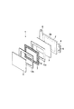
図1〜図4はこの発明の一実施例を示しており、図1は撮像素子ユニットの分解斜視図、図2は前記撮像素子ユニットの断面図である。 1 to 4 show an embodiment of the present invention. FIG. 1 is an exploded perspective view of an image sensor unit, and FIG. 2 is a sectional view of the image sensor unit.
この撮像素子ユニット1は、図1及び図2に示したように、固体撮像素子(CCD)2と、前記固体撮像素子2の前方に配置された位相格子型光学ローパスフィルタ6と、前記固体撮像素子2とローパスフィルタ6との間に配置されたスペーサ枠7とを備えている。
As shown in FIGS. 1 and 2, the
前記固体撮像素子2は、その前面に複数の撮像画素(図示せず)をマトリックス状に配列形成したものであり、この固体撮像素子2の前面つまり撮像面には、前記撮像面を保護するカバーガラス3が貼付けられ、後面には、実装用プレート4が取付けられている。なお、前記実装用プレート4の両端部は前記固体撮像素子2の両側の外方に突出しており、これらの突出部にねじ挿通孔5が設けられている。
The solid-state imaging device 2 has a plurality of imaging pixels (not shown) arranged in a matrix on the front surface thereof, and the front surface of the solid-state imaging device 2, that is, the imaging surface, is a cover that protects the imaging surface. The glass 3 is affixed and the
また、前記位相格子型光学ローパスフィルタ6は、透明なガラス板の一方の面に複数のローパスフィルタ素子(図示せず)をマトリックス状に配列形成したものである。
The phase grating optical low-
一方、前記スペーサ枠7は、前記固体撮像素子2の複数の撮像画素がマトリックス状に配列している撮像エリア2aを囲む矩形枠体からなっており、その両面間の厚さは、前記固体撮像素子2の撮像面と前記位相格子型光学ローパスフィルタ6との間の設計上の距離に応じて設定されている。
On the other hand, the
このスペーサ枠は、少なくとも前記枠体の内周と外周との間に通気性を有している。この実施例で用いたスペーサ枠7は、両面にそれぞれその内周縁から外周縁にわたる長さの複数の通気溝8を形成した枠体であり、前記複数の通気溝8内を通して空気を流通させる通気性を有している。
This spacer frame has air permeability at least between the inner periphery and the outer periphery of the frame body. The
また、この実施例では、前記スペーサ枠7を、シリコンゴム等の弾性材料からなる弾性枠としている。
In this embodiment, the
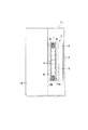
図3及び図4は前記スペーサ枠7の斜視図及びその一部分の拡大図であり、前記通気溝8は、その幅及び深さが10μm以下、好ましくは2〜5μmの細溝とされ、前記スペーサ枠7の各枠辺にそれぞれ略均等なピッチで形成されている。
3 and 4 are a perspective view of the
また、前記複数の通気溝8は、前記スペーサ枠7の両面にそれぞれ、その枠辺の長さ方向に対して30〜60度、好ましくは40〜50度の角度で斜めに交差する方向に沿わせて互いに平行に形成されている。
Further, the plurality of
さらに、前記複数の通気溝8の溝面にはそれぞれ、図4に示したように、例えばグリス等の非乾燥性油脂の塗布膜からなる異物付着膜9が、例えば0.5μm程度の極く薄い厚さに設けられている。
Further, as shown in FIG. 4, a foreign
そして、前記固体撮像素子2と位相格子型光学ローパスフィルタ6とは、図2に示したように、前記スペーサ枠7を介して貼合わされ、1つの撮像素子ユニット1とされている。
The solid-state image sensor 2 and the phase grating optical low-
なお、この実施例では、固体撮像素子2の前面(カバーガラス3の前面)と前記ローパスフィルタ6のフィルタ面とをそれぞれ、前記スペーサ枠7と略同じ枠形状の両面粘着テープ10a,10bにより前記スペーサ枠7の一方の面と他方の面とに貼付けている。
In this embodiment, the front surface of the solid-state imaging device 2 (the front surface of the cover glass 3) and the filter surface of the low-
上記撮像素子ユニット1は、薄型デジタルカメラに実装されるものであり、例えば、図2に示したように、図2に仮想線(二点鎖線)で示した前面が開口するケーシング11の内奥部に、ローパスフィルタ6を前記開口に向け、固体撮像素子2の後面の実装用プレート4を前記ケーシング11の内奥面にねじ止めして配置されるとともに、前記ケーシング11内の前側に撮像レンズ12を嵌装することにより、1つの撮像モジュールとされて図示しないカメラボディ内に実装される。
The
なお、図2では撮像レンズ12を簡略化して示しているが、この撮像レンズ12は、固定鏡胴と可動鏡胴とを有し、稼動撮像時にカメラボディの前面から突き出され、不使用時に引き込まれる沈胴型ズームレンズであり、前記撮像素子ユニット1は、前記ローパスフィルタ6を前記撮像レンズ12の後端に近接させて配置される。
Although the
前記撮像素子ユニット1は、固体撮像素子2と位相格子型光学ローパスフィルタ6とを、内周と外周との間に通気性を有するスペーサ枠7を介して貼合わせたものであるため、前記固体撮像素子2とローパスフィルタ6とを貼合わせて1つのユニットとしたものでありながら、温度変化による固体撮像素子2及びローパスフィルタ6の対向面、つまり固体撮像素子2の前面(カバーガラス3の前面)及びローパスフィルタ6の後面の曇りを無くして常に良好な撮像性能を維持することができる。
Since the
すなわち、固体撮像素子とローパスフィルタとを枠状に塗布した接着剤により接着した従来の撮像素子ユニットは、固体撮像素子とローパスフィルタとの間の空間が密閉されているため、例えば冬季に低温の屋外から暖房された屋内にデジタルカメラを持ち込んだときのように、カメラボディ内の温度、つまり撮像素子ユニット外の温度が急速に高くなっても、前記撮像素子ユニットの固体撮像素子とローパスフィルタとの間の空間内の温度は直ぐには変化せず、そのために、撮像素子ユニット外の温度と前記撮像素子ユニットの前記空間内の温度とに大きな差が生じて、前記空間内の空気中の水分が固体撮像素子及びローパスフィルタの対向面に結露して曇りを生じ、撮像性能を著しく低下させてしまう。 That is, in the conventional image sensor unit in which the solid-state image sensor and the low-pass filter are bonded with an adhesive applied in a frame shape, the space between the solid-state image sensor and the low-pass filter is sealed. Even when the temperature inside the camera body, that is, the temperature outside the image sensor unit rapidly rises like when a digital camera is brought indoors heated from the outside, the solid-state image sensor and the low-pass filter of the image sensor unit The temperature in the space between the two does not change immediately, so that there is a large difference between the temperature outside the image sensor unit and the temperature in the space of the image sensor unit, and moisture in the air in the space However, condensation occurs on the opposing surfaces of the solid-state imaging device and the low-pass filter, resulting in fogging, which significantly reduces imaging performance.
それに対して、上記実施例の撮像素子ユニット1は、固体撮像素子2とローパスフィルタ6とを、両面にそれぞれ内周縁から外周縁にわたる長さの複数の通気溝8を形成した通気性を有するスペーサ枠7を介して貼合わせたものであるため、前記撮像素子ユニット1の固体撮像素子2とローパスフィルタ6との間の空間内の温度が、前記空間内の空気と撮像素子ユニット1外の空気との相互流通により、撮像素子ユニット1外の温度変化に追従して変化する。
On the other hand, the image
そのため、この撮像素子ユニット1は、撮像素子ユニット1外の温度と前記空間内の温度とに大きな差が生じることは無く、したがって、例えば冬季に低温の屋外から暖房された屋内にデジタルカメラを持ち込んだときでも、固体撮像素子2及びローパスフィルタ6の対向面に曇りを生じさせること無く、良好な撮像性能を維持することができる。
Therefore, the
また、上記実施例では、前記スペーサ枠7を、シリコンゴム等の弾性材料からなる弾性枠としているため、例えば前記ケーシング11内への取付け作業中等に衝撃が加わったときでも、その衝撃を前記スペーサ枠7により吸収することができ、したがって、撮像素子ユニット1に耐衝撃性をもたせることができる。
Further, in the above embodiment, the
しかも、前記撮像素子ユニット1は、前記スペーサ枠7が弾性を有しているため、例えば撮像素子ユニット1の外側にローパスフィルタ6を固体撮像素子2側に引き寄せるねじ機構等を設けることにより、前記ローパスフィルタ6の引き寄せ力により前記スペーサ枠7を厚さ方向に弾性変形させて、前記固体撮像素子2の撮像面と前記ローパスフィルタ6との間の距離を微調整することができる。
Moreover, since the
また、前記撮像素子ユニット1は、前記スペーサ枠7の両面の通気溝8の幅及び深さを10μm以下(好ましくは2〜5μm)としているため、撮像素子ユニット1外から前記通気溝8内を通って固体撮像素子2とローパスフィルタ6との間の空間内に異物が入り込むのを防ぐことができ、したがって、固体撮像素子2による撮像画像に、外部からの異物の入り込みによる影欠陥を生じさせることは無い。
Further, since the
さらに、前記撮像素子ユニット1は、前記通気溝8を、前記スペーサ枠7の各枠辺にそれぞれ略均等なピッチで形成したものであるため、固体撮像素子2とローパスフィルタ6との間の空間内の空気と撮像素子ユニット1外の空気との相互流通量をさらに多くし、温度変化による固体撮像素子2及びローパスフィルタ6の対向面の曇りをさらに効果的に無くすことができるとともに、外部から衝撃が加わったときに、その衝撃力を前記スペーサ枠7の各通気溝8の間の部分に分散させて吸収させることができるため、撮像素子ユニット1の耐衝撃性をさらに良くすることができる。
Further, since the
また、前記撮像素子ユニット1は、前記通気溝8を、前記スペーサ枠7の枠辺の長さ方向に対して斜めに交差する方向に沿わせて形成しているため、前記通気溝8の長さを稼ぎ、外部からの異物の入り込みをさらに効果的に防ぐことができる。
Further, since the
さらに、前記撮像素子ユニット1は、前記スペーサ枠7の通気溝面にグリス等の非乾燥性油脂の塗布膜からなる異物付着膜9を設けているため、極く微細な異物が外部から前記通気溝8内に入り込んでも、その異物を前記異物付着膜9により吸着することができ、したがって、外部からの異物の入り込みをより確実に防ぐことができる。
Further, since the image
しかも、上記実施例では、固体撮像素子2の前面(カバーガラス3の前面)と前記ローパスフィルタ6のフィルタ面とをそれぞれ、前記スペーサ枠7と略同じ枠形状の両面粘着テープ10a,10bにより前記スペーサ枠7の一方の面と他方の面とに貼付けているため、外部から通気溝8内に入り込んだ微細な異物を、前記両面粘着テープ10a,10bの前記通気溝8内に露出している部分でも吸着することができ、したがって、外部からの異物の入り込みをさらに確実に防ぐことができる。
In addition, in the above embodiment, the front surface of the solid-state imaging device 2 (the front surface of the cover glass 3) and the filter surface of the low-
なお、上記実施例では、前記スペーサ枠7の両面にそれぞれ複数の通気溝8を、枠辺の長さ方向に対して斜めに交差する方向に沿わせて互いに平行に形成しているが、前記通気溝8は、図5に示した他の実施例のように、スペーサ枠7の枠辺の長さ方向に対して一方の方向に斜めに交差する方向と、前記枠辺の長さ方向に対して他方の方向に斜めに交差する方向との2つの方向に沿わせて網状に形成するのがより好ましく、このようにすることにより、外部からの異物の入り込みを効果的に防ぐとともに、固体撮像素子2とローパスフィルタ6との間の空間内の空気と撮像素子ユニット1外の空気との相互流通量を多くし、温度変化による固体撮像素子2及びローパスフィルタ6の対向面の曇りをより効果的に無くすことができる。
In the above embodiment, a plurality of
また、上記実施例では、スペーサ枠7の両面にそれぞれ複数の通気溝8を形成しているが、前記通気溝8は、固体撮像素子2の貼付け面とローパスフィルタ6の貼付け面のいずれか一方の面だけに形成してもよい。
Moreover, in the said Example, although the some ventilation groove |
さらに、上記実施例では、スペーサ枠7を、固体撮像素子2の貼付け面及びローパスフィルタ6の貼付け面(その少なくとも一方の面でもよい)に、その内周縁から外周縁にわたる長さの複数の通気溝8が形成された枠体としているが、固体撮像素子2とローパスフィルタ6との間に配置するスペーサ枠は、連続気泡を有する発泡ポリスチレンまたは発泡ポリウレタン等の発泡樹脂からなる枠体でもよく、このスペーサ枠を用いても、固体撮像素子2とローパスフィルタ6との間の空間内の温度を、この空間内と撮像素子ユニット1外の空気流通により撮像素子ユニット1外の温度変化に追従させて変化させ、温度変化による固体撮像素子2及びローパスフィルタ6の対向面の曇りを無くして常に良好な撮像性能を維持することができる。
Further, in the above embodiment, the
1…撮像素子ユニット、2…固体撮像素子、2a…撮像エリア、3…カバーガラス、4…実装用プレート、6…位相格子型光学ローパスフィルタ、7…スペーサ枠、8…通気溝、9…異物付着膜、10a,10b…両面粘着テープ、11…ケーシング、12…撮像レンズ。
DESCRIPTION OF
Claims (4)
前記固体撮像素子の前方に配置された光学フィルタと、
前記固体撮像素子の撮像エリアを囲む枠体からなり、前記固体撮像素子と前記光学フィルタとの間に配置され、該固体撮像素子の貼付け面と該光学フィルタの貼付け面の少なくとも一方に、その内周縁から外周縁にわたる長さであって、かつその枠辺の長さ方向に対して斜めに交差する方向に沿わせて複数の通気溝が形成されたスペーサ枠とを備え、
前記固体撮像素子と前記光学フィルタとを前記スペーサ枠を介して貼合わせたこと
を特徴とする撮像素子ユニット。 A solid-state image sensor;
An optical filter disposed in front of the solid-state image sensor;
The solid consists frame surrounding the imaging area of the imaging element, is arranged between the front Stories solid-state imaging element and said optical filter, at least one of the joining surfaces of the joining surface and the optical filter of the solid-state image capturing device, that A spacer frame having a length extending from the inner peripheral edge to the outer peripheral edge and formed with a plurality of ventilation grooves along a direction obliquely intersecting the length direction of the frame side;
An image sensor unit, wherein the solid-state image sensor and the optical filter are bonded together via the spacer frame.
前記固体撮像素子の前方に配置された光学フィルタと、
前記固体撮像素子の撮像エリアを囲む枠体からなり、前記固体撮像素子と前記光学フィルタとの間に配置され、該固体撮像素子の貼付け面と該光学フィルタの貼付け面の少なくとも一方に、その内周縁から外周縁にわたる長さであって、かつその枠辺の長さ方向に対して一方の方向に斜めに交差する方向と、前記枠辺の長さ方向に対して他方の方向に斜めに交差する方向との2つの方向に沿わせて網状に複数の通気溝が形成されたスペーサ枠とを備え、
前記固体撮像素子と前記光学フィルタとを前記スペーサ枠を介して貼合わせたこと
を特徴とする撮像素子ユニット。 A solid-state image sensor;
An optical filter disposed in front of the solid-state image sensor;
The solid consists frame surrounding the imaging area of the imaging element, is arranged between the front Stories solid-state imaging element and said optical filter, at least one of the joining surfaces of the joining surface and the optical filter of the solid-state image capturing device, that A length extending from the inner peripheral edge to the outer peripheral edge and obliquely intersecting one direction with respect to the length direction of the frame side, and obliquely extending in the other direction with respect to the length direction of the frame side A spacer frame having a plurality of ventilation grooves formed in a net shape along two directions of intersecting directions ,
An image sensor unit, wherein the solid-state image sensor and the optical filter are bonded together via the spacer frame.
前記固体撮像素子の前方に配置された光学フィルタと、
前記固体撮像素子の撮像エリアを囲む枠体からなり、前記固体撮像素子と前記光学フィルタとの間に配置され、該固体撮像素子の貼付け面と該光学フィルタの貼付け面の少なくとも一方に、その内周縁から外周縁にわたる長さの複数の通気溝が形成され、その通気溝面に異物付着膜が設けられているスペーサ枠とを備え、
前記固体撮像素子と前記光学フィルタとを前記スペーサ枠を介して貼合わせたこと
を特徴とする撮像素子ユニット。 A solid-state image sensor;
An optical filter disposed in front of the solid-state image sensor;
The solid consists frame surrounding the imaging area of the imaging element, is arranged between the front Stories solid-state imaging element and said optical filter, at least one of the joining surfaces of the joining surface and the optical filter of the solid-state image capturing device, that A plurality of ventilation grooves having a length extending from the inner peripheral edge to the outer peripheral edge, and a spacer frame provided with a foreign substance adhesion film on the ventilation groove surface ;
An image sensor unit, wherein the solid-state image sensor and the optical filter are bonded together via the spacer frame.
Priority Applications (1)
| Application Number | Priority Date | Filing Date | Title |
|---|---|---|---|
| JP2004282573A JP4552580B2 (en) | 2004-09-28 | 2004-09-28 | Image sensor unit |
Applications Claiming Priority (1)
| Application Number | Priority Date | Filing Date | Title |
|---|---|---|---|
| JP2004282573A JP4552580B2 (en) | 2004-09-28 | 2004-09-28 | Image sensor unit |
Publications (3)
| Publication Number | Publication Date |
|---|---|
| JP2006100425A JP2006100425A (en) | 2006-04-13 |
| JP2006100425A5 JP2006100425A5 (en) | 2007-07-19 |
| JP4552580B2 true JP4552580B2 (en) | 2010-09-29 |
Family
ID=36239967
Family Applications (1)
| Application Number | Title | Priority Date | Filing Date |
|---|---|---|---|
| JP2004282573A Expired - Fee Related JP4552580B2 (en) | 2004-09-28 | 2004-09-28 | Image sensor unit |
Country Status (1)
| Country | Link |
|---|---|
| JP (1) | JP4552580B2 (en) |
Cited By (1)
| Publication number | Priority date | Publication date | Assignee | Title |
|---|---|---|---|---|
| KR20160026633A (en) * | 2014-08-29 | 2016-03-09 | 에스에무케이 가부시키가이샤 | Camera module |
Families Citing this family (6)
| Publication number | Priority date | Publication date | Assignee | Title |
|---|---|---|---|---|
| JP2008011144A (en) * | 2006-06-29 | 2008-01-17 | Matsushita Electric Ind Co Ltd | Imaging apparatus |
| JP4064431B1 (en) * | 2006-09-26 | 2008-03-19 | シャープ株式会社 | Solid-state imaging device, manufacturing method thereof, and manufacturing device |
| KR101206560B1 (en) | 2010-01-05 | 2012-11-29 | 엘지이노텍 주식회사 | Voice coil motor |
| JP6085028B2 (en) * | 2013-07-30 | 2017-02-22 | 京セラ株式会社 | Imaging device mounting substrate and imaging device |
| JP2019066610A (en) * | 2017-09-29 | 2019-04-25 | ソニーセミコンダクタソリューションズ株式会社 | Imaging device, manufacturing method of imaging device, and electronic apparatus |
| CN112261552B (en) * | 2020-09-30 | 2021-12-24 | 瑞声新能源发展(常州)有限公司科教城分公司 | Sound production device, loudspeaker box and integrated hot press molding method |
Citations (4)
| Publication number | Priority date | Publication date | Assignee | Title |
|---|---|---|---|---|
| JP2003298033A (en) * | 2002-03-28 | 2003-10-17 | Fuji Photo Film Co Ltd | Imaging element |
| JP2004119881A (en) * | 2002-09-27 | 2004-04-15 | Sony Corp | Semiconductor device and its manufacturing method |
| JP2004187243A (en) * | 2002-12-06 | 2004-07-02 | Canon Inc | Image pickup device |
| JP2005039698A (en) * | 2003-07-18 | 2005-02-10 | Nikon Corp | Digital still camera |
-
2004
- 2004-09-28 JP JP2004282573A patent/JP4552580B2/en not_active Expired - Fee Related
Patent Citations (4)
| Publication number | Priority date | Publication date | Assignee | Title |
|---|---|---|---|---|
| JP2003298033A (en) * | 2002-03-28 | 2003-10-17 | Fuji Photo Film Co Ltd | Imaging element |
| JP2004119881A (en) * | 2002-09-27 | 2004-04-15 | Sony Corp | Semiconductor device and its manufacturing method |
| JP2004187243A (en) * | 2002-12-06 | 2004-07-02 | Canon Inc | Image pickup device |
| JP2005039698A (en) * | 2003-07-18 | 2005-02-10 | Nikon Corp | Digital still camera |
Cited By (2)
| Publication number | Priority date | Publication date | Assignee | Title |
|---|---|---|---|---|
| KR20160026633A (en) * | 2014-08-29 | 2016-03-09 | 에스에무케이 가부시키가이샤 | Camera module |
| KR102303163B1 (en) * | 2014-08-29 | 2021-09-15 | 에스에무케이 가부시키가이샤 | Camera module |
Also Published As
| Publication number | Publication date |
|---|---|
| JP2006100425A (en) | 2006-04-13 |
Similar Documents
| Publication | Publication Date | Title |
|---|---|---|
| US10670945B2 (en) | Drainage channel for a submersible camera with drainage ports on two surfaces | |
| JP4555732B2 (en) | Imaging device | |
| JP2018060161A (en) | Filter assembly and camera module having the same | |
| KR101455124B1 (en) | Image pickup apparatus having imaging sensor package | |
| US20040233318A1 (en) | Imager cover-glass mounting | |
| JP4552580B2 (en) | Image sensor unit | |
| CN208798223U (en) | Electronic equipment | |
| CN104349103A (en) | Digital video recorder | |
| TWM358314U (en) | Lens assemblies and photographic device | |
| EP1670238A4 (en) | Camera module | |
| JP2009244391A (en) | Lens assembly and imaging device | |
| EP1811772A3 (en) | Image sensor module having precise image-projection control | |
| JP3932565B2 (en) | Imaging device | |
| JP5899862B2 (en) | The camera module | |
| JP4031104B2 (en) | Stereo camera | |
| JP2009128890A (en) | Imaging apparatus | |
| JP2002277945A (en) | Waterproof camera, waterproof portable terminal device, and its dew condensation preventing method | |
| JP2011018954A (en) | Imaging device | |
| JP2006100425A5 (en) | ||
| JP2007194272A (en) | Imaging module | |
| KR101064666B1 (en) | Heating window assembly for camera | |
| US20110102988A1 (en) | Mounting structure for an electronic component and an electronic device | |
| JP2000216368A (en) | Infrared-ray cut filter attachment structure of image pickup device | |
| JP2007329813A (en) | Solid-state imaging apparatus and imaging apparatus provided with the solid-state imaging apparatus | |
| JP2898648B2 (en) | camera |
Legal Events
| Date | Code | Title | Description |
|---|---|---|---|
| A521 | Request for written amendment filed |
Free format text: JAPANESE INTERMEDIATE CODE: A523 Effective date: 20070531 |
|
| A621 | Written request for application examination |
Free format text: JAPANESE INTERMEDIATE CODE: A621 Effective date: 20070531 |
|
| A977 | Report on retrieval |
Free format text: JAPANESE INTERMEDIATE CODE: A971007 Effective date: 20100423 |
|
| A131 | Notification of reasons for refusal |
Free format text: JAPANESE INTERMEDIATE CODE: A131 Effective date: 20100511 |
|
| A521 | Request for written amendment filed |
Free format text: JAPANESE INTERMEDIATE CODE: A523 Effective date: 20100602 |
|
| TRDD | Decision of grant or rejection written | ||
| A01 | Written decision to grant a patent or to grant a registration (utility model) |
Free format text: JAPANESE INTERMEDIATE CODE: A01 Effective date: 20100622 |
|
| A01 | Written decision to grant a patent or to grant a registration (utility model) |
Free format text: JAPANESE INTERMEDIATE CODE: A01 |
|
| A61 | First payment of annual fees (during grant procedure) |
Free format text: JAPANESE INTERMEDIATE CODE: A61 Effective date: 20100705 |
|
| FPAY | Renewal fee payment (event date is renewal date of database) |
Free format text: PAYMENT UNTIL: 20130723 Year of fee payment: 3 |
|
| R150 | Certificate of patent or registration of utility model |
Ref document number: 4552580 Country of ref document: JP Free format text: JAPANESE INTERMEDIATE CODE: R150 Free format text: JAPANESE INTERMEDIATE CODE: R150 |
|
| LAPS | Cancellation because of no payment of annual fees |