JP4541627B2 - Micro mirror - Google Patents
Micro mirror Download PDFInfo
- Publication number
- JP4541627B2 JP4541627B2 JP2001549121A JP2001549121A JP4541627B2 JP 4541627 B2 JP4541627 B2 JP 4541627B2 JP 2001549121 A JP2001549121 A JP 2001549121A JP 2001549121 A JP2001549121 A JP 2001549121A JP 4541627 B2 JP4541627 B2 JP 4541627B2
- Authority
- JP
- Japan
- Prior art keywords
- mirror surface
- torsion
- micromirror
- mirror
- conductor
- Prior art date
- Legal status (The legal status is an assumption and is not a legal conclusion. Google has not performed a legal analysis and makes no representation as to the accuracy of the status listed.)
- Expired - Lifetime
Links
- 239000004020 conductor Substances 0.000 claims description 40
- 230000004907 flux Effects 0.000 claims description 5
- 238000004519 manufacturing process Methods 0.000 description 4
- 238000001465 metallisation Methods 0.000 description 4
- 238000010586 diagram Methods 0.000 description 3
- 238000000034 method Methods 0.000 description 3
- XUIMIQQOPSSXEZ-UHFFFAOYSA-N Silicon Chemical compound [Si] XUIMIQQOPSSXEZ-UHFFFAOYSA-N 0.000 description 2
- 238000011161 development Methods 0.000 description 2
- 230000018109 developmental process Effects 0.000 description 2
- 238000006073 displacement reaction Methods 0.000 description 2
- PCHJSUWPFVWCPO-UHFFFAOYSA-N gold Chemical compound [Au] PCHJSUWPFVWCPO-UHFFFAOYSA-N 0.000 description 2
- 239000010931 gold Substances 0.000 description 2
- 229910052737 gold Inorganic materials 0.000 description 2
- 229910052710 silicon Inorganic materials 0.000 description 2
- 239000010703 silicon Substances 0.000 description 2
- 238000005452 bending Methods 0.000 description 1
- 230000001419 dependent effect Effects 0.000 description 1
- 238000010292 electrical insulation Methods 0.000 description 1
- 238000000926 separation method Methods 0.000 description 1
- 230000003068 static effect Effects 0.000 description 1
- 235000012431 wafers Nutrition 0.000 description 1
- 238000004804 winding Methods 0.000 description 1
Images


Classifications
-
- G—PHYSICS
- G02—OPTICS
- G02B—OPTICAL ELEMENTS, SYSTEMS OR APPARATUS
- G02B26/00—Optical devices or arrangements for the control of light using movable or deformable optical elements
- G02B26/08—Optical devices or arrangements for the control of light using movable or deformable optical elements for controlling the direction of light
- G02B26/0816—Optical devices or arrangements for the control of light using movable or deformable optical elements for controlling the direction of light by means of one or more reflecting elements
- G02B26/0833—Optical devices or arrangements for the control of light using movable or deformable optical elements for controlling the direction of light by means of one or more reflecting elements the reflecting element being a micromechanical device, e.g. a MEMS mirror, DMD
- G02B26/085—Optical devices or arrangements for the control of light using movable or deformable optical elements for controlling the direction of light by means of one or more reflecting elements the reflecting element being a micromechanical device, e.g. a MEMS mirror, DMD the reflecting means being moved or deformed by electromagnetic means
-
- B—PERFORMING OPERATIONS; TRANSPORTING
- B81—MICROSTRUCTURAL TECHNOLOGY
- B81B—MICROSTRUCTURAL DEVICES OR SYSTEMS, e.g. MICROMECHANICAL DEVICES
- B81B3/00—Devices comprising flexible or deformable elements, e.g. comprising elastic tongues or membranes
- B81B3/0035—Constitution or structural means for controlling the movement of the flexible or deformable elements
- B81B3/004—Angular deflection
-
- G—PHYSICS
- G02—OPTICS
- G02B—OPTICAL ELEMENTS, SYSTEMS OR APPARATUS
- G02B26/00—Optical devices or arrangements for the control of light using movable or deformable optical elements
- G02B26/08—Optical devices or arrangements for the control of light using movable or deformable optical elements for controlling the direction of light
- G02B26/0816—Optical devices or arrangements for the control of light using movable or deformable optical elements for controlling the direction of light by means of one or more reflecting elements
- G02B26/0833—Optical devices or arrangements for the control of light using movable or deformable optical elements for controlling the direction of light by means of one or more reflecting elements the reflecting element being a micromechanical device, e.g. a MEMS mirror, DMD
- G02B26/0841—Optical devices or arrangements for the control of light using movable or deformable optical elements for controlling the direction of light by means of one or more reflecting elements the reflecting element being a micromechanical device, e.g. a MEMS mirror, DMD the reflecting element being moved or deformed by electrostatic means
-
- B—PERFORMING OPERATIONS; TRANSPORTING
- B81—MICROSTRUCTURAL TECHNOLOGY
- B81B—MICROSTRUCTURAL DEVICES OR SYSTEMS, e.g. MICROMECHANICAL DEVICES
- B81B2201/00—Specific applications of microelectromechanical systems
- B81B2201/04—Optical MEMS
- B81B2201/042—Micromirrors, not used as optical switches
-
- B—PERFORMING OPERATIONS; TRANSPORTING
- B81—MICROSTRUCTURAL TECHNOLOGY
- B81B—MICROSTRUCTURAL DEVICES OR SYSTEMS, e.g. MICROMECHANICAL DEVICES
- B81B2203/00—Basic microelectromechanical structures
- B81B2203/01—Suspended structures, i.e. structures allowing a movement
- B81B2203/0181—See-saws
-
- B—PERFORMING OPERATIONS; TRANSPORTING
- B81—MICROSTRUCTURAL TECHNOLOGY
- B81B—MICROSTRUCTURAL DEVICES OR SYSTEMS, e.g. MICROMECHANICAL DEVICES
- B81B2203/00—Basic microelectromechanical structures
- B81B2203/05—Type of movement
- B81B2203/058—Rotation out of a plane parallel to the substrate
-
- Y—GENERAL TAGGING OF NEW TECHNOLOGICAL DEVELOPMENTS; GENERAL TAGGING OF CROSS-SECTIONAL TECHNOLOGIES SPANNING OVER SEVERAL SECTIONS OF THE IPC; TECHNICAL SUBJECTS COVERED BY FORMER USPC CROSS-REFERENCE ART COLLECTIONS [XRACs] AND DIGESTS
- Y10—TECHNICAL SUBJECTS COVERED BY FORMER USPC
- Y10S—TECHNICAL SUBJECTS COVERED BY FORMER USPC CROSS-REFERENCE ART COLLECTIONS [XRACs] AND DIGESTS
- Y10S359/00—Optical: systems and elements
- Y10S359/904—Micromirror
Landscapes
- Physics & Mathematics (AREA)
- General Physics & Mathematics (AREA)
- Optics & Photonics (AREA)
- Electromagnetism (AREA)
- Engineering & Computer Science (AREA)
- Computer Hardware Design (AREA)
- Microelectronics & Electronic Packaging (AREA)
- Micromachines (AREA)
- Mechanical Light Control Or Optical Switches (AREA)
- Mechanical Optical Scanning Systems (AREA)
Description
【0001】
本発明は、請求項1の上位概念に記載されたマイクロミラー、殊にマイクロ振動ミラーに関する。
【0002】
従来の技術
静電駆動器を有するマイクロミラーおよび殊にマイクロ振動ミラーは、すでに特許明細書DE19857946.2に提案されている。ここでは十分に自由に支持されたミラー面と周囲の支持体とが接続されており、この接続は、対になって互いに向き合う2つまたは場合によっては4つのばねウェブまたはトーションビームによって行われる。
【0003】
US5748172からはさらに磁気駆動器を有するマイクロミラーがすでに公知である。ここでも同様に十分に自由に支持されたダイアフラムが、互いに向き合う2つのトーションビームを介して周囲の支持体に接続されている。ミラー面の下側には導体ループまたは巻線の形態の導体路が設けられていおり、これらを通して電流を流すことができ、これによって外部の磁界を加えれば、回転モーメントがミラー面に作用する。
【0004】
本発明の課題は、殊に磁気駆動器に対しても有利な機械的負荷容量の高い新しいミラー設計を開発することである。ここでこの高い機械的負荷容量をつぎのようにして達成する。すなわちミラー面を支持体に接続するトーションビームまたはばねウェブを、ねじれおよび振動に対して強くないしは負荷容量を大きく構成することによって高い機械的負荷容量を達成するのである。
【0005】
発明の利点
本発明のマイクロミラーは、従来技術に比して、高い機械的負荷容量と、破損に対する高い安定性を有するという利点を有し、同時にミラー面を静止位置から変位させるないしは励振してねじれ振動を発生させるために比較的低い電圧しか必要としない。
【0006】
さらに本発明のようにトーションビームを構成することによって有利にも、公知のマイクロミラーの場合に比して、ミラー面を変位させるために全体としてより大きな駆動力が必要であり、これは上記の高い安定性に結びつく。
【0007】
最後に本発明にしたがって少なくとも2つの、少なくとも近似的に平行に並んでガイドされるトーションビームを介してミラー面と支持体とを接続することより、同程度の曲げ強さであれば、これらの平行なトーションビームとその間にある中間空間との合計の幅を有する単一のトーションビームに比して、低減されたねじり剛性が得られる。これによって全体的なミラー設計の安定性を高めると同時にミラー面のより大きな変位角が可能になる。
【0008】
本発明の有利な発展形態は、従属請求項に記載されている。
【0009】
殊に有利であるのは、ミラー面を、互いに向き合う2つ側において、離隔して平行に並んでガイドされた2つのトーションビームによりそれぞれ支持体に接続する場合である。これにより各トーションビームの表面に導体路を被着することができ、ここでこの導体路はトーションビームの全面積を占めることができ、これにより導体路が互いに絶縁されるのと同時に、トーションビームの幅が最適に利用される。これによって殊に有利にも、トーションビームの表面に設けられた導体路を介して、例えば10mA〜1Aの殊に大きな電流を流すことができる。
【0010】
さらにトーションビームの表面に延在する導体路の幅をできる限り広くすることができる。それは導体路相互の電気的な絶縁という問題が生じないからである。
【0011】
幅を広くした導体路と、トーションビーム表面の最適利用とによって全体として高い電流負荷容量が得られ、これは磁気駆動器の場合に高い磁力ないしは回転モーメントに結びつく。したがって本発明によるマイクロミラーの設計によって比較的に大きな力が形成されることに起因して、有利にもトーションビームのより頑強な設計を選択することができる。
【0012】
したがって離隔して平行に並んでガイドされた2つのトーションビームと、その間にある中間空間とを合計した全体的な幅は、従来技術から公知の相応する単一のトーションビームの幅よりも大きい。
【0013】
さらに本発明のばね設計では、2つのトーションビームと所属の中間空間との合計の幅を有する単一のトーションビームのねじり剛性よりも低いねじり剛性が得られ有利である。
【0014】
上記のばね設計は、この他に、互いに垂直な2つのねじり軸を有するマイクロミラーに有利に転用することもできる。
【0015】
さらに、トーションビームの表面の導体路と、部分的に支持体に設けられるコンタクト面と、ミラー面の表面でガイドされる導体路とを、表面メタライゼーションのそれ自体公知の方法によって簡単に形成することができ有利である。
【0016】
さらに本発明のマイクロミラーは、静電駆動器にも磁気駆動器にも備え付けることができる。
【0017】
最後に、実際のミラー面が、外側の領域に対称に取り付けられた2つのループを有することによってつぎのような利点が得られる。すなわちこれらのループを同時にミラー面に対するストッパとして使用することができ、ひいてはこれらと、殊にトーションビームとを衝突および一時的な過負荷から保護することできることである。ここで上記のループにより、ミラー面の表面でガイドされる導体路によって包囲される、外部の磁界の磁束が格段に増大する。このために有利にはミラー面が過剰にねじれた際、これらのループが上部ないしは下部のケーシング面または支持体に当接して、トーションビームの折れが阻止されるようにする。
【0018】
ミラー面のこれらの付加的なループが殊に有利であるのは、本発明のマイクロミラーを静的に変位させたい場合、およびできる限り小さなエアーダンパーを達成するためにミラー面と周囲の支持体との間に空隙を設ける場合である。
【0019】
要約すると本発明のマイクロミラーは、大きな駆動力が小さな駆動電圧で得られるという利点を有し、ここでは同時にマイクロミラーの改善された安定性と、作製の際の高い歩留まりとが得られる。それは形成されるマイクロ構造体が全体的に比較的頑強だからである。この他に本発明のマイクロミラーは完全にそれ自体公知の作製手法によって作製することができ、このため加工の際に新たな方法ステップおよび作製技術は不要である。
【0020】
図面
本発明を以下、図面に基づき詳しく説明する。
【0021】
図1は、静電駆動器を有するマイクロミラーの第1実施例を示しており、図2は、磁気駆動器を有する第2実施形態を示しており、図3は、磁気駆動器を有するマイクロミラーの第3実施形態を示している。
【0022】
実施例
図1は、マイクロ振動ミラーの形態で実施されたマイクロミラー5を示している。
【0023】
さらに詳しくいうと、例えばシリコン製の支持体11,12からそれ自体公知のように図示のマイクロミラー5が加工構造化される。典型的には100μm×100μm〜400μm×400μmのサイズを有する矩形のミラー面10が設けられ、これらのミラー面の互いに向き合う2つの面には、離隔して平行に並んでガイドされた2つずつのトーションビーム13,13′が設けられている。ばねウェブとして作用するトーションビーム13,13′によって、ミラー面10と、このミラー面を例えば側方において、かつ下方の領域において包囲する支持体11,12とが接続され、これによってミラー面10は十分に自由に支持される。また支持体11,12は例えばシリコンウェーハである。
【0024】
さらにトーションビーム13,13′は10μm〜100μmの長さと、2μm〜10μmの高さと、5μm〜15μmの幅とを有している。さらにこれらは2μm〜5μmの間隔で互いに平行に配置されており、これによってこの間隔に相応する中間空間が、トーションビーム13,13′の間に生じる。
【0025】
ミラー面10の下には静電駆動器を実現するための電極面があり、これの一部に公知のように電極18が被着されている。さらにこのミラー面には少なくとも一部に、例えば下側にメタライゼーション部を有しており、これらはトーションビーム13,13′によってガイドされる導体路を介して外部の電圧供給部に接続されている。
【0026】
これにより、電圧を電極18ないしはミラー面10に印加することによって、静電気力をミラー面10と電極18との間に作用させることができ、トーションビーム13,13′によって定められる軸に平行なねじれ軸17の周りでミラー面10が変位する。
【0027】
図1の実施例についてのさらなる説明、殊にマイクロミラー5の作製、電気的な制御および端子接続についてのさらなる詳細は省略する。それはこれらの詳細は当業者には公知だからである。
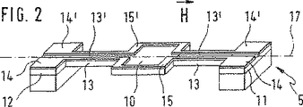
【0028】
図2は、図1の実施例の択一的な実施形態を示しており、ここでは静電駆動器の代わりに磁気駆動器が使用されている。このためにミラー面10の表面の少なくとも一方の側に導体路15,15′が設けられている。これらの導体路は有利にはミラー面の外側の周縁部をガイドされ、これによってこれらの導体路により、できる限り大きな面積がミラー面10において取り囲まれるようにする。導体路15,15′は、例えば公知のように表面メタライゼーション、例えば金からなる表面メタライゼーションを部分的に被着することによって形成される。図2の導体路15,15′ができる限り大きな電流に耐られるようにするため、さらに有利であるのは、導体路15,15′できる限り厚くかつ平らに構成することである。
【0029】
導体路15,15′は、ミラー面10を出発してそれぞれ対応するトーションビーム13ないしは13′を介して電気的なコンタクト面14,14′にガイドされる。これらは例えば公知のように支持体11,12に被着されている。ここで各導体路15,15′は、それらにそれぞれ対応付けられたトーションビーム13ないしは13′の全面積を占める。
【0030】
2つの導体路15,15′の電気的な分離は、トーションビーム13,13′の間に設けられている中間空間によって保証される。
【0031】
導体路15,15′の厚さは、有利には100nm〜2μmであるが、10μmに達することも可能である。その幅は有利には5μm〜50μmである。その他に導体路15,15′は有利には金からなる。
【0032】
図2において、記入されたシンボルHによってさらに示されているのは、図2のマイクロミラー5が外部の磁界内にあることである。
【0033】
マイクロミラー5の動作時には、例えば10V〜30Vの外部の電圧を、隣り合う2つのコンタクト面14,14′に印加することにより、また反対側の残りの2つのコンタクト面14,14′を用いて電流路を閉じることにより、例えば10mA〜500mAの電流Iが導体路15,15′を流れ、これによって、説明した導体路15,15′の配置構成により、ミラー面10のサイズによって定められる面積Aを取り囲む閉じられた導体ループが形成される。
【0034】
したがって加えられた電流Iと、外部の磁界Hとによって回転モーメントTがミラー面10に作用し、ここではつぎが成り立つ。すなわち
【0035】
【数1】

したがって加えられる電流I,外部の磁界BないしはHの強度、および導体ループによって取り囲まれた面積Aに比例するこの回転モーメントTは、ねじり軸17の周りのミラー面10の旋回ないしはねじれを発生させる。これにより、加えられる電流Iおよび/または外部の磁界Hを適切に、例えば周期的に変化させることによって簡単にミラー面10のねじり振動を励振することができる。
【0037】
しかしながら説明した実施例は、明らかにミラー面10の静的な変位にも有利である。
【0038】
全部をひっくるめると、ミラー面10にできる限り大きな力ないしはできる限り大きな回転モーメントを達成するために、説明した実施例において有利であるのは、導体路15,15′をミラー面10の表面の少なくとも一方の側に案内して、外部の磁界Hのできる限り多くの磁束が、導体路15,15′によって取り囲まれるようにすることである。
【0039】
図3では、図2の発展形態で本発明の別の実施例が説明されている。この実施例は、図2とつぎの点だけが異なる。すなわちミラー面10は、支持体11,12からの相応する有利な加工構造化によって、側方のループ16,16′を有する点だけが図2と異なるのである。ループ16,16′は有利には対称に配置されており、導体路15,15′によって取り囲まれる面積が増すことによって、取り囲まれる磁束を増大させるないしは回転モーメントを増大させるためにもっぱら使用される。
【0040】
図3のループ16,16′は、例えば500μm〜1mmの全長と、100μm〜500μmの全幅とを有している。その厚さはミラー面10の厚さに等しい。ループ16,16′はさらにトーションビーム13,13′と類似に形成されている。すなわちこれらは空間を取り囲む狭いウェブの形状を有しており、ここでこのウェブの表面にはそれぞれ対応する導体路15ないしは15′が延在しており、これらの導体路によって有利には表面が完全に覆われている。
【0041】
図3のミラー面10がループ16,16′を有することによって、電流路を閉じた際に発生する導体ループは全体として比較的大きな面積を取り囲み、このため電流Iと磁界Hとが同じであれば、格段に大きな回転トルクTを形成することができる。
【0042】
また加えられる外部の磁界は、有利には1mTesla〜1000mTestlaの強度を有し、かつ例えばミラー面10の周囲に配置される永久磁石または電磁石によって形成される。
【図面の簡単な説明】
【図1】 静電駆動器を有するマイクロミラーの第1実施例を示す図である。
【図2】 磁気駆動器を有する第2実施形態を示す図である。
【図3】 磁気駆動器を有するマイクロミラーの第3実施形態を示す図である。[0001]
The invention relates to a micromirror, in particular a micro-vibrating mirror, as described in the superordinate concept of claim 1.
[0002]
A micromirror with a prior art electrostatic drive and in particular a microvibrating mirror has already been proposed in the patent specification DE 19857946.2. Here, a sufficiently freely supported mirror surface and the surrounding support are connected, this connection being made by two or possibly four spring webs or torsion beams which face each other in pairs.
[0003]
US Pat. No. 5,748,172 already discloses a micromirror with a magnetic drive. Here again, a sufficiently freely supported diaphragm is connected to the surrounding support via two torsion beams facing each other. A conductor path in the form of a conductor loop or a winding is provided below the mirror surface, and an electric current can flow through them, so that when an external magnetic field is applied, a rotational moment acts on the mirror surface.
[0004]
The object of the present invention is to develop a new mirror design with a high mechanical load capacity which is particularly advantageous for magnetic drives. Here, this high mechanical load capacity is achieved as follows. That is, a high mechanical load capacity is achieved by configuring the torsion beam or spring web connecting the mirror surface to the support to be strong against torsion and vibration or to increase the load capacity.
[0005]
Advantages of the Invention The micromirror of the present invention has the advantages of higher mechanical load capacity and higher stability against breakage than the prior art, and at the same time displace or excite the mirror surface from a stationary position. Only a relatively low voltage is required to generate torsional vibration.
[0006]
Furthermore, advantageously by constructing a torsion beam as in the present invention, a greater driving force is required as a whole to displace the mirror surface than in the case of known micromirrors, which is the above-mentioned high It leads to stability.
[0007]
Finally, by connecting the mirror surface and the support via at least two torsion beams guided in parallel at least approximately in parallel according to the present invention, these parallels can be obtained with similar bending strength. A reduced torsional stiffness is obtained compared to a single torsion beam having the total width of the torsion beam and the intermediate space between them. This increases the stability of the overall mirror design while allowing a larger displacement angle of the mirror surface.
[0008]
Advantageous developments of the invention are described in the dependent claims.
[0009]
It is particularly advantageous when the mirror surface is connected to the support by two torsion beams guided in parallel and spaced apart on two sides facing each other. This allows a conductor track to be deposited on the surface of each torsion beam, where the conductor track can occupy the entire area of the torsion beam, thereby isolating the conductor tracks from each other and simultaneously reducing the width of the torsion beam. Used optimally. In this way, a particularly large current of, for example, 10 mA to 1 A can be applied via a conductor track provided on the surface of the torsion beam.
[0010]
Furthermore, the width of the conductor path extending on the surface of the torsion beam can be made as wide as possible. This is because the problem of electrical insulation between the conductor paths does not occur.
[0011]
Overall, a high current load capacity is obtained by the wide conductor path and the optimal use of the torsion beam surface, which leads to a high magnetic or rotational moment in the case of a magnetic driver. Therefore, a more robust design of the torsion beam can advantageously be selected due to the relatively large force created by the design of the micromirror according to the invention.
[0012]
The total width of the two torsion beams guided in parallel and spaced apart and the intermediate space between them is therefore greater than the width of the corresponding single torsion beam known from the prior art.
[0013]
Furthermore, the spring design of the present invention advantageously provides a torsional stiffness that is lower than the torsional stiffness of a single torsion beam having the combined width of the two torsion beams and the associated intermediate space.
[0014]
In addition to this, the spring design described above can also be advantageously transferred to a micromirror having two torsion axes perpendicular to each other.
[0015]
Furthermore, the conductor track on the surface of the torsion beam, the contact surface partially provided on the support, and the conductor track guided on the surface of the mirror surface can be easily formed by a method known per se for surface metallization. This is advantageous.
[0016]
Furthermore, the micromirror of the present invention can be provided in both an electrostatic drive and a magnetic drive.
[0017]
Finally, the following advantages are obtained by having the actual mirror surface have two loops mounted symmetrically in the outer region. That is, these loops can be used simultaneously as a stop for the mirror surface and thus protect them and in particular the torsion beam from collisions and temporary overloads. Here, the magnetic flux of the external magnetic field surrounded by the conductor path guided by the surface of the mirror surface is greatly increased by the loop. For this purpose, advantageously, when the mirror surface is excessively twisted, these loops abut against the upper or lower casing surface or support so that the torsion beam is prevented from breaking.
[0018]
These additional loops of the mirror surface are particularly advantageous if the micromirror of the present invention is to be statically displaced, and in order to achieve the smallest possible air damper, the mirror surface and the surrounding support In this case, a gap is provided between the two.
[0019]
In summary, the micromirrors of the present invention have the advantage that a large driving force can be obtained with a small driving voltage, which at the same time provides an improved stability of the micromirror and a high yield in production. This is because the formed microstructure is relatively robust overall. In addition to this, the micromirror of the present invention can be completely produced by a production method known per se, so that no new method steps and production techniques are required for processing.
[0020]
The present invention will be described in detail below with reference to the drawings.
[0021]
FIG. 1 shows a first example of a micromirror having an electrostatic driver, FIG. 2 shows a second embodiment having a magnetic driver, and FIG. 3 shows a micromirror having a magnetic driver. 3 shows a third embodiment of a mirror.
[0022]
EXAMPLE FIG. 1 shows a
[0023]
More specifically, for example, the
[0024]
Further, the
[0025]
Below the
[0026]
Thereby, an electrostatic force can be applied between the
[0027]
A further description of the embodiment of FIG. 1, in particular further details on the production of the
[0028]
FIG. 2 shows an alternative embodiment of the example of FIG. 1, in which a magnetic driver is used instead of an electrostatic driver. For this purpose,
[0029]
The conductor tracks 15, 15 'start from the
[0030]
The electrical separation of the two conductor tracks 15, 15 'is ensured by an intermediate space provided between the torsion beams 13, 13'.
[0031]
The thickness of the conductor tracks 15, 15 ′ is preferably between 100 nm and 2 μm, but can reach 10 μm. Its width is preferably between 5 μm and 50 μm. In addition, the conductor tracks 15, 15 'are preferably made of gold.
[0032]
In FIG. 2, what is further indicated by the symbol H entered is that the
[0033]
When the
[0034]
Therefore, the rotational moment T acts on the
[Expression 1]
Thus, this rotational moment T, which is proportional to the applied current I, the strength of the external magnetic field B or H, and the area A surrounded by the conductor loop, causes the
[0037]
However, the described embodiment is also advantageous for static displacement of the
[0038]
In order to achieve the greatest possible force or rotational moment as much as possible on the
[0039]
In FIG. 3, another embodiment of the invention is illustrated in the development of FIG. This embodiment differs from FIG. 2 only in the following points. That is, the
[0040]
3 has a total length of, for example, 500 μm to 1 mm and a total width of 100 μm to 500 μm. Its thickness is equal to the thickness of the
[0041]
Since the
[0042]
The applied external magnetic field preferably has a strength of 1 mTesla to 1000 mTestla and is formed, for example, by a permanent magnet or an electromagnet arranged around the
[Brief description of the drawings]
FIG. 1 is a diagram showing a first embodiment of a micromirror having an electrostatic driver.
FIG. 2 is a diagram showing a second embodiment having a magnetic driver.
FIG. 3 is a diagram showing a third embodiment of a micromirror having a magnetic driver.
Claims (6)
前記ミラー面(10)は、少なくとも近似的に平行に並んでガイドされた少なくとも2つのトーションビーム(13,13′)を介して、少なくとも1つの支持体(11,12)に接続されている形式のマイクロミラーにおいて、
前記ミラー面(10)の少なくとも一部分は、表面に導体路(15,15′)を有しており、
前記のミラー面(10)は、回転トルクおよび/または磁束を増加させるために少なくとも1つのループ(16,16’)を有しており、該ループの表面に導体路(15,15’)が1つずつ延在しており、外部の磁場(H)のできる限りに多くの磁束を、前記の導体路(15,15’)によって取り囲み、当該の導体路(15,15’)を通して電流が導かれる際には回転モーメントを前記のミラー面(10)に及ぼすようにしたことを特徴とする、
マイクロミラー。A micromirror having a freely supported mirror surface (10) displaceable from a rest position about at least one torsion axis (17),
The mirror surface (10) is of the type connected to at least one support (11, 12) via at least two torsion beams (13, 13 ') guided at least approximately in parallel. In the micro mirror,
At least a part of the mirror surface (10) has a conductor track (15, 15 ') on the surface ,
Said mirror surface (10) has at least one loop (16, 16 ') to increase the rotational torque and / or magnetic flux, and a conductor track (15, 15') on the surface of the loop. Each of them extends, and as much magnetic flux as possible of the external magnetic field (H) is surrounded by the conductor path (15, 15 ′), and current is passed through the conductor path (15, 15 ′). When guided, the rotational moment is exerted on the mirror surface (10) ,
Micro mirror.
請求項1に記載のマイクロミラー。The torsion beams (13, 13 ') are guided in parallel and spaced apart from each other,
The micromirror according to claim 1.
前記の2つずつのトーションビーム(13,13′)は、離隔して並んで配置されており、
前記の4つのトーションビーム(13,13′)は共通のねじり軸(17)を定める、
請求項1または2に記載のマイクロミラー。The mirror surface (10) is connected to the support (11, 12) via four torsion beams (13, 13 '),
The two torsion beams (13, 13 ') are arranged apart from each other,
The four torsion beams (13, 13 ') define a common torsion axis (17),
The micromirror according to claim 1 or 2.
該支持体(11,12)は、少なくとも1つのコンタクト面(14,14′)を有する、
請求項1から3までのいずれか1項に記載のマイクロミラー。The mirror surface (10) is electrically connected to the support (11, 12) via at least one conductor track (15, 15 '),
The support (11, 12) has at least one contact surface (14, 14 '),
The micromirror according to any one of claims 1 to 3 .
請求項1から4までのいずれか1項に記載のマイクロミラー。 Said conductor track is electrically connected to the support (11, 12) via a torsion beam (13, 13 '),
The micromirror according to any one of claims 1 to 4 .
請求項5に記載のマイクロミラー。Each said conductor track (15, 15 ') extends flatly on at least one side of the surface of the associated torsion beam (13, 13'), and the said torsion beam (13, 13 ') Covering at least part of the surface,
The micromirror according to claim 5 .
Applications Claiming Priority (3)
| Application Number | Priority Date | Filing Date | Title |
|---|---|---|---|
| DE19963382.7 | 1999-12-28 | ||
| DE19963382A DE19963382A1 (en) | 1999-12-28 | 1999-12-28 | Micromirror |
| PCT/DE2000/004116 WO2001048527A2 (en) | 1999-12-28 | 2000-11-22 | Micromirror |
Publications (3)
| Publication Number | Publication Date |
|---|---|
| JP2003518650A JP2003518650A (en) | 2003-06-10 |
| JP2003518650A5 JP2003518650A5 (en) | 2007-09-20 |
| JP4541627B2 true JP4541627B2 (en) | 2010-09-08 |
Family
ID=7934753
Family Applications (1)
| Application Number | Title | Priority Date | Filing Date |
|---|---|---|---|
| JP2001549121A Expired - Lifetime JP4541627B2 (en) | 1999-12-28 | 2000-11-22 | Micro mirror |
Country Status (6)
| Country | Link |
|---|---|
| US (1) | US6749308B1 (en) |
| EP (1) | EP1247131B1 (en) |
| JP (1) | JP4541627B2 (en) |
| DE (2) | DE19963382A1 (en) |
| ES (1) | ES2228650T3 (en) |
| WO (1) | WO2001048527A2 (en) |
Families Citing this family (57)
| Publication number | Priority date | Publication date | Assignee | Title |
|---|---|---|---|---|
| US5910854A (en) | 1993-02-26 | 1999-06-08 | Donnelly Corporation | Electrochromic polymeric solid films, manufacturing electrochromic devices using such solid films, and processes for making such solid films and devices |
| US5668663A (en) | 1994-05-05 | 1997-09-16 | Donnelly Corporation | Electrochromic mirrors and devices |
| US6891563B2 (en) | 1996-05-22 | 2005-05-10 | Donnelly Corporation | Vehicular vision system |
| US6124886A (en) | 1997-08-25 | 2000-09-26 | Donnelly Corporation | Modular rearview mirror assembly |
| US8294975B2 (en) | 1997-08-25 | 2012-10-23 | Donnelly Corporation | Automotive rearview mirror assembly |
| US6326613B1 (en) | 1998-01-07 | 2001-12-04 | Donnelly Corporation | Vehicle interior mirror assembly adapted for containing a rain sensor |
| US6172613B1 (en) | 1998-02-18 | 2001-01-09 | Donnelly Corporation | Rearview mirror assembly incorporating vehicle information display |
| US6445287B1 (en) | 2000-02-28 | 2002-09-03 | Donnelly Corporation | Tire inflation assistance monitoring system |
| US8288711B2 (en) | 1998-01-07 | 2012-10-16 | Donnelly Corporation | Interior rearview mirror system with forwardly-viewing camera and a control |
| US6477464B2 (en) | 2000-03-09 | 2002-11-05 | Donnelly Corporation | Complete mirror-based global-positioning system (GPS) navigation solution |
| US6693517B2 (en) | 2000-04-21 | 2004-02-17 | Donnelly Corporation | Vehicle mirror assembly communicating wirelessly with vehicle accessories and occupants |
| US6329925B1 (en) | 1999-11-24 | 2001-12-11 | Donnelly Corporation | Rearview mirror assembly with added feature modular display |
| US7370983B2 (en) | 2000-03-02 | 2008-05-13 | Donnelly Corporation | Interior mirror assembly with display |
| WO2007053710A2 (en) | 2005-11-01 | 2007-05-10 | Donnelly Corporation | Interior rearview mirror with display |
| AU2001243285A1 (en) | 2000-03-02 | 2001-09-12 | Donnelly Corporation | Video mirror systems incorporating an accessory module |
| US7167796B2 (en) | 2000-03-09 | 2007-01-23 | Donnelly Corporation | Vehicle navigation system for use with a telematics system |
| US7255451B2 (en) | 2002-09-20 | 2007-08-14 | Donnelly Corporation | Electro-optic mirror cell |
| US7581859B2 (en) | 2005-09-14 | 2009-09-01 | Donnelly Corp. | Display device for exterior rearview mirror |
| EP1363810B1 (en) | 2001-01-23 | 2007-05-30 | Donnelly Corporation | Improved vehicular lighting system |
| US6918674B2 (en) | 2002-05-03 | 2005-07-19 | Donnelly Corporation | Vehicle rearview mirror system |
| EP1514246A4 (en) | 2002-06-06 | 2008-04-16 | Donnelly Corp | Interior rearview mirror system with compass |
| US7329013B2 (en) | 2002-06-06 | 2008-02-12 | Donnelly Corporation | Interior rearview mirror system with compass |
| US7310177B2 (en) | 2002-09-20 | 2007-12-18 | Donnelly Corporation | Electro-optic reflective element assembly |
| EP1543358A2 (en) | 2002-09-20 | 2005-06-22 | Donnelly Corporation | Mirror reflective element assembly |
| CN100350294C (en) * | 2002-10-10 | 2007-11-21 | 富士通株式会社 | Micro moving element comprising torsion bar |
| US7177068B2 (en) | 2002-12-20 | 2007-02-13 | Robert Bosch Gmbh | Apparatus, method and system for providing enhanced mechanical protection for thin beams |
| US7014115B2 (en) | 2003-08-25 | 2006-03-21 | Advanced Nano Systems, Inc. | MEMS scanning mirror with distributed hinges and multiple support attachments |
| US7446924B2 (en) | 2003-10-02 | 2008-11-04 | Donnelly Corporation | Mirror reflective element assembly including electronic component |
| US7308341B2 (en) | 2003-10-14 | 2007-12-11 | Donnelly Corporation | Vehicle communication system |
| US7706046B2 (en) * | 2004-06-08 | 2010-04-27 | Gentex Corporation | Rearview mirror element having a circuit mounted to the rear surface of the element |
| US7864398B2 (en) | 2004-06-08 | 2011-01-04 | Gentex Corporation | Electro-optical element including metallic films and methods for applying the same |
| EP1883855B1 (en) | 2005-05-16 | 2011-07-20 | Donnelly Corporation | Vehicle mirror assembly with indicia at reflective element |
| DE102005033800B4 (en) * | 2005-07-13 | 2016-09-15 | Fraunhofer-Gesellschaft zur Förderung der angewandten Forschung e.V. | Micromechanical optical element with a reflective surface and its use |
| US7643196B2 (en) | 2005-12-16 | 2010-01-05 | The Charles Stark Draper Laboratory, Inc. | Systems, methods and devices for actuating a moveable miniature platform |
| US7746534B2 (en) * | 2006-12-07 | 2010-06-29 | Gentex Corporation | Thin-film coatings, electro-optic elements and assemblies incorporating these elements |
| EP2426552A1 (en) | 2006-03-03 | 2012-03-07 | Gentex Corporation | Electro-optic elements incorporating improved thin-film coatings |
| US7688495B2 (en) * | 2006-03-03 | 2010-03-30 | Gentex Corporation | Thin-film coatings, electro-optic elements and assemblies incorporating these elements |
| US8368992B2 (en) * | 2006-03-03 | 2013-02-05 | Gentex Corporation | Electro-optical element including IMI coatings |
| US8274729B2 (en) * | 2006-03-03 | 2012-09-25 | Gentex Corporation | Thin-film coatings, electro-optic elements and assemblies incorporating these elements |
| US8169681B2 (en) | 2006-03-03 | 2012-05-01 | Gentex Corporation | Thin-film coatings, electro-optic elements and assemblies incorporating these elements |
| TWI328139B (en) * | 2007-01-22 | 2010-08-01 | Ind Tech Res Inst | Projector |
| US8035881B2 (en) * | 2007-03-05 | 2011-10-11 | Gentex Corporation | Multi-zone mirrors |
| US9274394B2 (en) | 2007-03-05 | 2016-03-01 | Gentex Corporation | Multi-zone mirrors |
| US10017847B2 (en) * | 2007-03-05 | 2018-07-10 | Gentex Corporation | Method and apparatus for ion milling |
| US8649083B2 (en) | 2007-03-05 | 2014-02-11 | Gentex Corporation | Multi-zone mirrors |
| US8196874B2 (en) * | 2007-10-12 | 2012-06-12 | Maxtec, Llc | Storable intravenous stands |
| JP2009229916A (en) * | 2008-03-24 | 2009-10-08 | Nippon Telegr & Teleph Corp <Ntt> | Micromirror element and micro mirror array |
| US8154418B2 (en) | 2008-03-31 | 2012-04-10 | Magna Mirrors Of America, Inc. | Interior rearview mirror system |
| DE102008026886B4 (en) * | 2008-06-05 | 2016-04-28 | Fraunhofer-Gesellschaft zur Förderung der angewandten Forschung e.V. | Process for structuring a wear layer of a substrate |
| DE102013210059B4 (en) * | 2013-05-29 | 2021-07-01 | Fraunhofer-Gesellschaft zur Förderung der angewandten Forschung e.V. | Device with a spring and an optical element suspended from it |
| CN105712290B (en) * | 2014-12-04 | 2017-09-29 | 无锡华润上华半导体有限公司 | The preparation method of MEMS electrostatic actuators |
| DE102015216811B4 (en) | 2015-09-02 | 2023-06-29 | Robert Bosch Gmbh | Pivoting device for a micromirror |
| DE102016220514A1 (en) * | 2016-10-19 | 2018-04-19 | Robert Bosch Gmbh | Micromechanical component and production method for a micromechanical component |
| DE102016013227A1 (en) * | 2016-11-07 | 2018-05-09 | Blickfeld GmbH | Fiber scanner with at least two fibers |
| DE102016221966A1 (en) | 2016-11-09 | 2018-05-09 | Robert Bosch Gmbh | Method for controlling an actuator device and micromechanical device |
| DE102017206252A1 (en) | 2017-04-11 | 2018-10-11 | Fraunhofer-Gesellschaft zur Förderung der angewandten Forschung e.V. | Micromechanical mirror device |
| CN116100845A (en) * | 2023-01-06 | 2023-05-12 | 四川大学 | Method for integrating 3D printing torsion Liang Weixing with scanning micro-mirror |
Family Cites Families (13)
| Publication number | Priority date | Publication date | Assignee | Title |
|---|---|---|---|---|
| JP3003429B2 (en) * | 1992-10-08 | 2000-01-31 | 富士電機株式会社 | Torsional vibrator and optical deflector |
| GB2275787A (en) | 1993-03-05 | 1994-09-07 | British Aerospace | Silicon micro-mirror unit |
| EP0657760A1 (en) * | 1993-09-15 | 1995-06-14 | Texas Instruments Incorporated | Image simulation and projection system |
| US5665997A (en) * | 1994-03-31 | 1997-09-09 | Texas Instruments Incorporated | Grated landing area to eliminate sticking of micro-mechanical devices |
| JP3425814B2 (en) * | 1994-12-28 | 2003-07-14 | 日本信号株式会社 | Electromagnetic actuator and method of manufacturing the same |
| US5670977A (en) * | 1995-02-16 | 1997-09-23 | Texas Instruments Incorporated | Spatial light modulator having single bit-line dual-latch memory cells |
| KR100343219B1 (en) * | 1995-02-25 | 2002-11-23 | 삼성전기주식회사 | Apparatus for driving mirror |
| US6046840A (en) * | 1995-06-19 | 2000-04-04 | Reflectivity, Inc. | Double substrate reflective spatial light modulator with self-limiting micro-mechanical elements |
| US5739941A (en) * | 1995-07-20 | 1998-04-14 | Texas Instruments Incorporated | Non-linear hinge for micro-mechanical device |
| US6072617A (en) * | 1996-11-26 | 2000-06-06 | Texas Instruments Incorporated | Micro mechanical device with memory metal component |
| DE19728598C2 (en) | 1997-07-04 | 2000-12-14 | Bosch Gmbh Robert | Micromechanical mirror device |
| US6201629B1 (en) * | 1997-08-27 | 2001-03-13 | Microoptical Corporation | Torsional micro-mechanical mirror system |
| DE19857946C1 (en) | 1998-12-16 | 2000-01-20 | Bosch Gmbh Robert | Micro vibrating mirror for displays, scanners and optical monitoring systems |
-
1999
- 1999-12-28 DE DE19963382A patent/DE19963382A1/en not_active Ceased
-
2000
- 2000-11-22 WO PCT/DE2000/004116 patent/WO2001048527A2/en active IP Right Grant
- 2000-11-22 ES ES00988634T patent/ES2228650T3/en not_active Expired - Lifetime
- 2000-11-22 US US10/169,247 patent/US6749308B1/en not_active Expired - Lifetime
- 2000-11-22 DE DE50007817T patent/DE50007817D1/en not_active Expired - Lifetime
- 2000-11-22 EP EP00988634A patent/EP1247131B1/en not_active Expired - Lifetime
- 2000-11-22 JP JP2001549121A patent/JP4541627B2/en not_active Expired - Lifetime
Also Published As
| Publication number | Publication date |
|---|---|
| EP1247131B1 (en) | 2004-09-15 |
| DE50007817D1 (en) | 2004-10-21 |
| WO2001048527A2 (en) | 2001-07-05 |
| US6749308B1 (en) | 2004-06-15 |
| DE19963382A1 (en) | 2001-07-12 |
| EP1247131A2 (en) | 2002-10-09 |
| WO2001048527A3 (en) | 2002-02-14 |
| ES2228650T3 (en) | 2005-04-16 |
| JP2003518650A (en) | 2003-06-10 |
Similar Documents
| Publication | Publication Date | Title |
|---|---|---|
| JP4541627B2 (en) | Micro mirror | |
| KR100702019B1 (en) | Micro mirror device | |
| EP1411024B1 (en) | 2-D actuator and manufacturing method thereof | |
| JP4602542B2 (en) | Mirror oscillator for optical deflector | |
| JP4544972B2 (en) | Optical deflector | |
| JP4550578B2 (en) | Micro movable element with torsion bar | |
| EP3029508B1 (en) | Mirror drive device | |
| JP4262574B2 (en) | Optical deflector | |
| JP2012528343A (en) | Micromachining type component and method of manufacturing the micromachining type component | |
| JPWO2004017119A1 (en) | Micro oscillating device with torsion bar | |
| JP2005173411A (en) | Light deflector | |
| KR20090098801A (en) | Micromirror actuator with encapsulation possibilty and method for production thereof | |
| ITTO20010519A1 (en) | ADJUSTABLE DEVICE, IN PARTICULAR RIGID DISC ACTUATOR DEVICE, WITH CONTROL OF THE ROLLING AND PICKING ANGLE. | |
| US20050231787A1 (en) | Micro-oscillation element | |
| WO2006022967A1 (en) | Mems mirror with amplification of mirror rotation angle | |
| EP2706393B1 (en) | Optical deflector including narrow piezoelectric sensor element between torsion bar and piezoelectric actuator | |
| EP1128540A1 (en) | Structure for electrically connecting microelectromechanical devices,in particular microactuators for hard disk drives | |
| JP2024050649A (en) | Actuator device and method for manufacturing actuator device | |
| JP2000171481A (en) | Comb structure, actuator and inertia sensor | |
| US6747786B2 (en) | Optical deflector and optical deflector array | |
| JP2019530019A (en) | Micromirror device and method of operating micromirror device | |
| JP4102343B2 (en) | 2-axis actuator with large area stage | |
| US7821693B1 (en) | MEMS mirror with rotation amplification and electromagnetic drive | |
| CN112204450B (en) | Light deflector | |
| JP3846359B2 (en) | Optical device |
Legal Events
| Date | Code | Title | Description |
|---|---|---|---|
| A521 | Request for written amendment filed |
Free format text: JAPANESE INTERMEDIATE CODE: A523 Effective date: 20070720 |
|
| A621 | Written request for application examination |
Free format text: JAPANESE INTERMEDIATE CODE: A621 Effective date: 20070720 |
|
| A131 | Notification of reasons for refusal |
Free format text: JAPANESE INTERMEDIATE CODE: A131 Effective date: 20091016 |
|
| A521 | Request for written amendment filed |
Free format text: JAPANESE INTERMEDIATE CODE: A523 Effective date: 20100114 |
|
| A131 | Notification of reasons for refusal |
Free format text: JAPANESE INTERMEDIATE CODE: A131 Effective date: 20100205 |
|
| A521 | Request for written amendment filed |
Free format text: JAPANESE INTERMEDIATE CODE: A523 Effective date: 20100428 |
|
| TRDD | Decision of grant or rejection written | ||
| A01 | Written decision to grant a patent or to grant a registration (utility model) |
Free format text: JAPANESE INTERMEDIATE CODE: A01 Effective date: 20100526 |
|
| A01 | Written decision to grant a patent or to grant a registration (utility model) |
Free format text: JAPANESE INTERMEDIATE CODE: A01 |
|
| A61 | First payment of annual fees (during grant procedure) |
Free format text: JAPANESE INTERMEDIATE CODE: A61 Effective date: 20100624 |
|
| R150 | Certificate of patent or registration of utility model |
Ref document number: 4541627 Country of ref document: JP Free format text: JAPANESE INTERMEDIATE CODE: R150 Free format text: JAPANESE INTERMEDIATE CODE: R150 |
|
| FPAY | Renewal fee payment (event date is renewal date of database) |
Free format text: PAYMENT UNTIL: 20130702 Year of fee payment: 3 |
|
| R250 | Receipt of annual fees |
Free format text: JAPANESE INTERMEDIATE CODE: R250 |
|
| R250 | Receipt of annual fees |
Free format text: JAPANESE INTERMEDIATE CODE: R250 |
|
| R250 | Receipt of annual fees |
Free format text: JAPANESE INTERMEDIATE CODE: R250 |
|
| R250 | Receipt of annual fees |
Free format text: JAPANESE INTERMEDIATE CODE: R250 |
|
| R250 | Receipt of annual fees |
Free format text: JAPANESE INTERMEDIATE CODE: R250 |
|
| R250 | Receipt of annual fees |
Free format text: JAPANESE INTERMEDIATE CODE: R250 |
|
| R250 | Receipt of annual fees |
Free format text: JAPANESE INTERMEDIATE CODE: R250 |
|
| R250 | Receipt of annual fees |
Free format text: JAPANESE INTERMEDIATE CODE: R250 |
|
| EXPY | Cancellation because of completion of term |