JP4531447B2 - Surface inspection device - Google Patents
Surface inspection device Download PDFInfo
- Publication number
- JP4531447B2 JP4531447B2 JP2004165671A JP2004165671A JP4531447B2 JP 4531447 B2 JP4531447 B2 JP 4531447B2 JP 2004165671 A JP2004165671 A JP 2004165671A JP 2004165671 A JP2004165671 A JP 2004165671A JP 4531447 B2 JP4531447 B2 JP 4531447B2
- Authority
- JP
- Japan
- Prior art keywords
- light
- irradiation
- light receiving
- measurement object
- optical system
- Prior art date
- Legal status (The legal status is an assumption and is not a legal conclusion. Google has not performed a legal analysis and makes no representation as to the accuracy of the status listed.)
- Expired - Fee Related
Links
Images


Classifications
-
- G—PHYSICS
- G01—MEASURING; TESTING
- G01B—MEASURING LENGTH, THICKNESS OR SIMILAR LINEAR DIMENSIONS; MEASURING ANGLES; MEASURING AREAS; MEASURING IRREGULARITIES OF SURFACES OR CONTOURS
- G01B11/00—Measuring arrangements characterised by the use of optical techniques
- G01B11/30—Measuring arrangements characterised by the use of optical techniques for measuring roughness or irregularity of surfaces
- G01B11/306—Measuring arrangements characterised by the use of optical techniques for measuring roughness or irregularity of surfaces for measuring evenness
-
- G—PHYSICS
- G01—MEASURING; TESTING
- G01N—INVESTIGATING OR ANALYSING MATERIALS BY DETERMINING THEIR CHEMICAL OR PHYSICAL PROPERTIES
- G01N21/00—Investigating or analysing materials by the use of optical means, i.e. using sub-millimetre waves, infrared, visible or ultraviolet light
- G01N21/84—Systems specially adapted for particular applications
- G01N21/88—Investigating the presence of flaws or contamination
- G01N21/95—Investigating the presence of flaws or contamination characterised by the material or shape of the object to be examined
- G01N21/9501—Semiconductor wafers
Landscapes
- Physics & Mathematics (AREA)
- General Physics & Mathematics (AREA)
- Health & Medical Sciences (AREA)
- Life Sciences & Earth Sciences (AREA)
- Chemical & Material Sciences (AREA)
- Analytical Chemistry (AREA)
- Biochemistry (AREA)
- General Health & Medical Sciences (AREA)
- Immunology (AREA)
- Pathology (AREA)
- Length Measuring Devices By Optical Means (AREA)
- Investigating Materials By The Use Of Optical Means Adapted For Particular Applications (AREA)
Description
本発明は、測定対象物の表面の状態を検出する表面検査装置の改良に関する。 The present invention relates to an improvement in a surface inspection apparatus that detects a surface state of a measurement object.
従来から、表面検査装置には、測定対象物に反りがあってもその測定対象物の表面に存在する異物、キズ等の位置を正確に検出するために、測定対象物の表面に存在する異物、キズの高さ方向の位置を検出する構成のものが知られている(例えば、特許文献1参照。)。 Conventionally, in order to accurately detect the position of foreign matter, scratches, etc. present on the surface of the measurement target even if the measurement target is warped, the surface inspection apparatus has a foreign matter present on the surface of the measurement target. A configuration for detecting a position in the height direction of a scratch is known (for example, see Patent Document 1).
このものでは、例えば、図1に示すように、照射光源1から出射された照射光P1を測定対象物としてのウェハ2に照射する照射光学系3と、照射光学系3により照射されたウェハ2の表面Sの異物、キズ等による散乱光P2を受光して光電変換信号に変換する受光素子4を有する受光光学系5と、照射光学系3により照射されたウェハ2の表面Sからの正反射光P3を受光して光電変換信号に変換する受光素子6を有する受光光学系7とを備えている。
In this device, for example, as shown in FIG. 1, an irradiation
そのウェハ2は、相対変位手段としての回転駆動機構8、直線移動機構部9を用いて照射光学系3、受光光学系5、7に対する相対変位が与えられる。その回転駆動機構8、直線駆動機構9はそれぞれ駆動モータを有する。
The
このものによれば、図2に示すように、基準高さZ1に位置するウェハ2の表面を符号Sで示し、基準高さZ1に対して高さ方向(Z方向)にΔZだけ高さがずれているウェハ2の表面を符号S’で示し、表面Sに異物10が存在するときの検出位置y1からの正反射光P3が第2受光素子6の受光基準位置Q0に入射するものとしたとき、ウェハ2の表面S’からの正反射光P3’の受光素子6における受光位置は、受光基準位置Q0に対してΔSだけずれた位置Q1になり、ずれ量ΔSとずれ量ΔZの間には一定の関係があるので、このずれ量ΔSと反射角度θとから、表面Sが基準高さ位置Z1にあるとしたときの異物10の照射検出位置である半径方向の平面座標位置y1に対して表面Sが高さΔZだけ符号S’で示すように基準高さZ1からずれたとしたときの平面座標位置y2のずれ量Δyは、式
Δy=ΔS/tanθ
又は、式
Δy=ΔZ/tanθ
によって求まる。
According to this, as shown in FIG. 2, the surface of the
Or the equation Δy = ΔZ / tanθ
It is obtained by.
従って、照射検出位置が基準高さZ1に対してΔZだけずれたときの平面座標位置y2は、式
y2=y1−Δy
を用いて求まる。
Accordingly, the plane coordinate position y2 when the irradiation detection position is shifted by ΔZ with respect to the reference height Z1 is expressed by the equation y2 = y1−Δy.
Is obtained using.
すなわち、ウェハ2に反りがある場合であっても、ウェハ2に存在するその異物12のy方向の平面座標位置を補正により正確に検出できる。
ところが、測定対象物としてのウェハ2の表面Sが粗面の場合、表面Sの凹凸Rによる局所的な傾きにより、図3に示すように、照射光P1の表面Sによる正反射光P3が本来凹凸Rがないとしたならば反射される方向であろう方向P4に対して符号P5で示すように振れてずれることがある。
However, when the surface S of the
このため、従来のものでは、このように表面Sが粗面の場合には、ウェハ2の異物10の照射検出位置が基準高さ位置Z1からずれているのかずれていないのか区別できないという問題がある。
For this reason, in the conventional apparatus, when the surface S is rough as described above, it is impossible to distinguish whether the irradiation detection position of the
本発明は、上記の事情に鑑みて為されたもので、その目的とするところは、測定対象物の表面が粗面であっても、測定対象物の照射検出位置が基準高さからずれているのかいないのかの区別を行うことができるようにした表面検査装置を提供するところにある。 The present invention has been made in view of the above circumstances, and the object of the present invention is that even if the surface of the measurement object is rough, the irradiation detection position of the measurement object deviates from the reference height. It is an object of the present invention to provide a surface inspection apparatus capable of distinguishing between being and not present.
請求項1に記載の表面検査装置は、光源からの照射光を測定対象物の表面に照射する照射光学系と前記測定対象物の表面により反射された散乱光を受光する受光光学系とを含む光学系と、前記測定対象物の表面への前記光学系による照射検出位置を相対変位させる相対変位手段と、前記光学系の受光結果に基づき前記測定対象物の表面の状態を検出すると共に前記測定対象物の表面への照射検出位置を平面座標位置として記録する記録手段と、前記平面座標位置の基準高さ位置に対するずれ量を検出する高さ方向ずれ量検出手段と、前記高さ方向ずれ量検出手段によるずれ量に基づき前記照射検出位置である平面座標位置を補正して前記平面座標位置を求める処理手段とを備え、
前記照射光学系は照射光軸が互いに平行なマルチビームを前記測定対象物の表面に向けて集束照射するマルチビーム照射光学系を備え、前記高さ方向ずれ量検出手段は、受光軸が互いに平行でかつ前記測定対象物の表面により反射されたマルチビームをそれぞれ受光する受光素子が設けられた集光光学系を備え、前記処理手段は前記マルチビームの受光結果に基づき前記表面の粗面に関する状態情報を解析処理すると共に、該解析処理結果に基づき前記基準高さ位置に対するずれ量から前記表面の粗面による影響を除去したうえで、前記測定対象物の照射検出位置が基準高さ位置にあるとしたときの前記各受光素子の受光基準位置と実際の受光位置との差に基づいて前記照射検出位置の実際の高さ位置における平面座標位置を求める処理を行うことを特徴とする。
請求項2に記載の表面検査装置は、前記相対変位手段は前記測定対象物を回転させる回転駆動機構と、前記測定対象物を半径方向に直線的に移動させる直線移動機構とを備え、前記照射光軸は前記半径方向に並列的に配列され、前記受光光軸は前記測定対象物の回転中心を挟んで対称的に配列されていることを特徴とする。
請求項3に記載の表面検査装置は、前記各受光素子がエリアセンサにより構成されていることを特徴とする。
請求項4に記載の表面検査装置は、前記状態情報が粗面情報又は表面歪み情報であることを特徴とする。
The surface inspection apparatus according to claim 1 includes an irradiation optical system that irradiates the surface of the measurement object with irradiation light from a light source and a light receiving optical system that receives the scattered light reflected by the surface of the measurement object. An optical system, a relative displacement means for relatively displacing an irradiation detection position by the optical system on the surface of the measurement object, and a state of the surface of the measurement object based on a light reception result of the optical system and the measurement Recording means for recording the irradiation detection position on the surface of the object as a plane coordinate position, a height direction deviation amount detection means for detecting a deviation amount of the plane coordinate position with respect to a reference height position, and the height direction deviation amount Processing means for correcting the plane coordinate position, which is the irradiation detection position, based on the deviation amount by the detection means, and obtaining the plane coordinate position;
The irradiation optical system includes a multi-beam irradiation optical system that focuses and irradiates multi-beams whose irradiation optical axes are parallel to each other toward the surface of the object to be measured. And a condensing optical system provided with a light receiving element for receiving each of the multi-beams reflected by the surface of the measurement object, and the processing means is in a state related to the rough surface of the surface based on the light-receiving result of the multi-beams. Analyzing the information and removing the influence of the rough surface from the amount of deviation with respect to the reference height position based on the result of the analysis processing, the irradiation detection position of the measurement object is at the reference height position line processing for obtaining a planar coordinate position in the the the actual height position of the irradiation position detection based on the difference between the actual light receiving position and the light-receiving reference position of the light receiving element when It is characterized in.
The surface inspection apparatus according to
The surface inspection apparatus according to
The surface inspection apparatus according to
請求項1ないし請求項4に記載の表面検査装置によれば、測定対象物の表面が粗面であってもまた歪みがあっても、測定対象物の表面に存在する異物、キズ等の照射検出位置が基準高さからずれているのかいないかの区別を行うことができ、かつ、測定対象物の表面が粗面であってもその影響を除去して基準高さ位置からずれ量を検出でき、従って、測定対象物の表面が粗面であってもその影響を取り除いて、異物の検出位置である平面座標位置を補正により正確に求めることができる。 According to the surface inspection apparatus according to any one of claims 1 to 4, even if the surface of the measurement object is rough or distorted, irradiation of foreign matter or scratches existing on the surface of the measurement object is possible. It is possible to distinguish whether the detection position is deviated from the reference height, and even if the surface of the measurement object is rough, the influence is removed and the deviation amount is detected from the reference height position. Therefore, even if the surface of the measurement object is a rough surface, the influence can be removed, and the plane coordinate position that is the detection position of the foreign matter can be accurately obtained by correction.
以下に、本発明に係わる表面検査装置の実施例を図面を参照しつつ説明する。 Embodiments of a surface inspection apparatus according to the present invention will be described below with reference to the drawings.
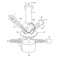
図4は本発明に係わる表面検査装置の概要図である。この図4において、11は測定対象物としてのウェハ2を回転駆動させる回転駆動機構、12は照射光学系、13、14は受光光学系、15は集光光学系である。そのウェハ2はその回転駆動機構11によって回転軸O1を中心に矢印M方向に回転駆動されると共に、図示を略す直線移動機構によって矢印y方向に移動され、この回転駆動機構11と直線移動機構(図示を略す)とからなる相対変位手段によって、ウェハ2の表面Sへの光学系による照射検出位置が相対変位される。
FIG. 4 is a schematic view of a surface inspection apparatus according to the present invention. In FIG. 4, 11 is a rotation drive mechanism for rotating the
照射光学系12は、複数個の光源、ここでは、図5に示すように、3個のレーザ光源12a〜12cと、この3個のレーザ光源12a〜12cから発生したレーザービームを集光・整形して基準高さ位置Z1におけるウェハ2の表面Sに照射光P6〜P8として集束させる集束レンズ12d〜12fとから概略構成され、照射光学系12は照射光P6〜P8としてのマルチレーザビームをウェハ2の表面Sの照射検出位置に向けて照射するマルチビーム照射光学系としての役割を果たす。
The irradiation
受光光学系13、14(図4参照)は、ここでは、3個のレーザ光源12a〜12cのうちのレーザ光源12bによる照射光の異物、キズ等の表面状態に起因する散乱光束を受光するように設けられており、図9に示すように受光素子としての光電変換素子13a、14aを有する。その受光光学系13、14の構成は、従来の構造と変わらないので、ここでは、その詳細な説明は省略する。
Here, the light receiving
集光光学系15は、ここでは、マルチレーザビームの個数に対応する個数の集光レンズ15a〜15cと、この集光レンズ15a〜15cにより集光された受光光束を検出する受光素子15d〜15fとから概略構成されている。
Here, the condensing
その集光光学系15は、ウェハ2の表面Sの照射検出位置からの照射光P6〜P8による反射光P6’〜P8’をそれぞれ集光し、各受光素子15d〜15fはその反射光P6’〜P8’をそれぞれ受光可能に設けられている。その受光素子15d〜15fは、ここではエリアセンサから構成されている。
The condensing
レーザ光源12a〜12cの照射光軸(主光線)は互いに平行に設けられ、その照射光軸はウェハ2の半径方向に並列的に配列されている。受光素子15d〜15fの受光光軸は回転中心O1を挟んで照射光軸と対称的に配列されている。その図5において、符号Q2〜Q4はその表面Sが光学的に理想的な平面でありかつ表面Sが基準高さ位置Z1にあるときの受光基準位置を示している。
Irradiation optical axes (principal rays) of the
その集光光学系15は、表面Sの基準高さ位置Z1に対するずれ量ΔZを検出する高さ方向ずれ量検出手段の一部として機能する。
The condensing
ウェハ2の表面Sが基準高さ位置Z1にあるものとして、その表面Sが粗面でなく、光学的に理想的な平滑面であるとしたとき、照射光学系12の照射光軸上を通る照射光P6〜P8の反射光P6’〜P8’は、その表面Sにおいて正反射され、受光素子15d〜15fの受光基準位置Q2〜Q4にピークが生じるようにして受光される。
Assuming that the surface S of the
ところが、表面Sが粗面であるとき、言い換えると、表面Sに凹凸Rがあるときには、照射光P6〜P8は凹凸Rの影響を受けて、例えば、受光基準位置Q2〜Q4からずれた受光位置Q2’〜Q4’にピークが生じるようにして受光される。 However, when the surface S is rough, in other words, when the surface S has unevenness R, the irradiated light P6 to P8 is affected by the unevenness R, for example, a light receiving position shifted from the light receiving reference positions Q2 to Q4. Light is received such that peaks occur at Q2 'to Q4'.
従って、各受光素子15d〜15fの受光基準位置Q2〜Q4からの各ずれ量ΔS1〜ΔS3に基づいて、表面Sに凹凸Rが存在するか否かを識別できる。
Therefore, it is possible to identify whether or not the unevenness R exists on the surface S based on the shift amounts ΔS1 to ΔS3 from the light receiving reference positions Q2 to Q4 of the
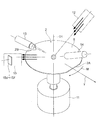
また、その凹凸Rの湾曲方向によってその反射方向が変わるため、図6に示すように、受光素子15d、15e、15fの受光面上での受光スポット像N1〜N3の結像位置が二次元的に変化する。その図6において、例えば、受光スポット像N1は表面Sの照射検出位置である平面座標位置y3により反射された照射光P8に基づく反射光P6’が受光素子15dに結像することにより形成されたものに対応し、受光スポット像N2は表面Sの平面座標位置y4により反射された照射光P7に基づく反射光P7’が受光素子15eに結像することにより形成されたものに対応し、受光スポット像N3は表面Sの平面座標位置y5により反射された照射光P6に基づく反射光P8’が受光素子15fに結像することにより形成されたものに対応する。
Further, since the reflection direction changes depending on the curve direction of the unevenness R, as shown in FIG. 6, the imaging positions of the light receiving spot images N1 to N3 on the light receiving surfaces of the
これに対して、ウェハ2の表面が図7(a)に示すように基準高さ位置Z1から一様にΔZだけずれているときには、照射光P6〜P8が基準高さ位置Z1における表面Sにピントを結ぶ前にその表面Sにおいて反射され、かつ、その表面Sの平面座標系での照射検出位置も基準高さ位置Z1における表面Sの平面座標系での照射検出位置から一様にΔyだけずれることになる。
On the other hand, when the surface of the
これに応じて、その照射光P6〜P8の反射光P6’〜P8’も図7(b)に示すように受光基準位置Q2〜Q4からΔyだけ一様に同じ方向にずれて受光されると共に、その反射光P6’〜P8’のボケ量も一様となると考えられる。その図7(b)において、例えば、符号N4は受光素子15dの受光面上でのスポット像、符号N5は受光素子15e上でのスポット像、符号N6は受光素子15fの受光面上でのスポット像、符号T1はその表面Sが基準高さ位置Z1にあるとしたときに反射光P6’により受光素子15dに形成されたスポット像の光量分布、符号T2はその表面Sが基準高さ位置Z1にあるとしたときに反射光P7’により受光素子15eに形成されたスポット像の光量分布、符号T3はその表面Sが基準高さ位置Z1にあるとしたときに反射光P8’により受光素子15fに形成されたスポット像の光量分布、符号T1’はその表面Sが基準高さ位置Z1から高さ方向にΔZだけずれた位置にあるとしたときに反射光P6’により受光素子15dに形成されたスポット像の光量分布、符号T2’はその表面Sが基準高さ位置Z1から高さ方向にΔZだけずれた位置にあるとしたときに反射光P7’により受光素子15eに形成されたスポット像の光量分布、符号T3はその表面Sが基準高さ位置Z1から高さ方向にΔZだけずれた位置にあるとしたときに反射光P8’により受光素子15fに形成されたスポット像の光量分布である。この図7(b)は、表面Sが基準高さ位置Z1からΔZだけ高さ方向にずれたときには、いずれも光量分布T1’〜T3’のピークが同じ方向に同量ずれていることを示している。
In response to this, the reflected lights P6 ′ to P8 ′ of the irradiated lights P6 to P8 are also received by being shifted by Δy uniformly in the same direction from the light receiving reference positions Q2 to Q4 as shown in FIG. 7B. The amount of blur of the reflected lights P6 ′ to P8 ′ is considered to be uniform. In FIG. 7B, for example, the symbol N4 is a spot image on the light receiving surface of the
その一方、ウェハ21の表面S’が図8(a)に示すように湾曲していて、例えば、表面S’の平面座標系の照射検出位置yxにおける基準高さ位置Z1からのずれ量ΔZ1がもっとも大きく、表面S’の平面座標系の照射検出位置y3における基準高さ位置Z1からのずれ量ΔZ2が表面S’の照射検出位置yxと照射検出位置y5におけるずれ量ΔZ3との間の中間にあり、照射検出位置y5の基準高さ位置Z1からのずれ量ΔZ3が0のとき、照射検出位置y5で反射された照射光束P6の反射光P8’は受光素子15fの受光基準位置Q4においてピントの合った状態で受光され、照射検出位置y3で反射された照射光P7の反射光P7’は受光素子15eの受光基準位置Q3からΔS2だけずれた位置で受光され、このΔS2はのずれ量ΔZ2に比例する。また、照射検出位置y3で反射された反射光P7’は受光素子15e上でピントのぼけた状態で結像される。
On the other hand, the surface S ′ of the
表面Sの照射検出位置yxで反射された反射光P6’は、図8(b)に示すように受光素子15dの受光基準位置Q2からΔS1だけずれた位置で受光され、このΔS1はずれ量ΔZ1に比例する。また、照射検出位置yxで反射された反射光P6’は、受光素子15d上でピントのぼけた状態で結像され、この受光素子15d上でのピントのぼけ量は受光素子15e上でのピントのぼけ量よりも大きい。なお、その図8(b)において、符号T1’はその表面Sが基準高さ位置Z1から高さ方向にΔZ1だけずれた位置にあるとしたときに反射光P6’により受光素子15dに形成されたスポット像による光量分布、符号T2’はその表面Sが基準高さ位置Z1から高さ方向にΔZ2だけずれた位置にあるとしたときに反射光P7’により受光素子15eに形成されたスポット像による光量分布、符号T3はその表面Sが基準高さ位置Z1から高さ方向にΔZ3だけずれた位置にあるとしたときに反射光P8’により受光素子15fに形成されたスポット像による光量分布である。
The reflected light P6 ′ reflected at the irradiation detection position yx on the surface S is received at a position shifted by ΔS1 from the light receiving reference position Q2 of the
従って、表面Sに湾曲や反りがあるが光学的に滑らかな面の場合には、その各受光素子15d〜15fの受光基準位置Q0からのずれ量ΔSが、表面基準高さZ1からのずれ量ΔZに比例し、その受光基準位置Q0からのずれの方向も同じである。これに対して、表面Sの湾曲や反りの中に凹凸Rが存在するときにはそのずれの方向及びその量がランダムにばらつくことになる。
Accordingly, when the surface S is curved or warped but is an optically smooth surface, the shift amount ΔS of each of the
よって、受光素子15d〜15fのエリアセンサ上での光量分布のパターンから高さ情報、粗面情報を解析処理することができる。
Therefore, the height information and the rough surface information can be analyzed from the pattern of the light amount distribution on the area sensors of the
その各受光素子15d〜15fからの受光信号は、図9に示すように処理手段としての処理回路に入力される。この処理回路は、高さ位置検出回路部16a〜16c、アナログデジタル変換回路部17a〜17c、バッファメモリ部18a〜18c、演算回路部19を有する。
The light receiving signals from the
その各受光素子15d〜15fからの受光信号は、高さ位置検出回路部16a〜16cに入力され、高さ位置検出回路部16a〜16cは各受光信号に基づき受光基準位置Q0に対するX方向アナログ情報とY方向アナログ情報とを出力し、そのX方向アナログ情報とY方向アナログ情報とはアナログデジタル変換回路部17a〜17cによりアナログデジタル変換されてデジタル信号としてバッファメモリ部18a〜18cに入力され、このバッファメモリ部18a〜18cを介して演算回路部29に入力される。
The light reception signals from the respective
各受光素子15d〜15fにはエリアセンサが用いられているので、ウェハ2の表面の三次元的光量分布情報が得られ、このエリアセンサの各素子毎の光量分布情報が演算回路部19に入力されるので、ウェハ2の表面Sにより反射された照射光P6〜P8による反射光P6’〜P8’のぼけ量に関する情報(粗面情報)、ピーク情報が求まることになる。
Since an area sensor is used for each of the
演算回路部19には、またエンコーダ信号ENが入力される。このエンコーダ信号ENは、ウェハ2の測定開始基準位置からクロックパルス数を出力するもので、時系列的に等間隔に出力される。ウェハ2は相対変位手段により回転されると共に半径方向に送られるので、そのエンコーダ信号ENに基づき検出位置である表面Sの平面座標位置が螺旋状に決定される。
The encoder signal EN is also input to the
演算回路部19は、その平面座標位置と関連づけてその検出位置における高さ情報Z(基準高さ位置Z1からのずれ量ΔZ)、粗面情報をメモリ部20に記憶させる。
The
光電変換素子13a、14aの受光信号は増幅回路部(AMP回路部)21に入力され、この増幅回路部21による増幅信号はアナログデジタル変換(A/D変換)回路部22によりA/D変換され、ピーク検出回路23にデジタル信号として入力される。
The light reception signals of the
そのピーク検出回路部23には、A/D変換されたデジタル信号と共にエンコーダ信号ENが入力され、ピーク検出回路部23はそのエンコーダ信号ENに基づきピーク位置を平面座標位置情報と関連づけて演算同期回路部24に向けて出力する。演算同期回路部24はその結果をメモリ部25に向けて出力し、メモリ部25にはその表面Sの照射検出位置毎にピーク位置情報が保存される。
The peak
その演算同期回路24は、メモリ部25、演算回路部19との間で情報の授受を行い、メモリ部25に保存されている平面座標位置情報と、メモリ部20に保存されている高さ情報(ずれ量ΔZ)、平面座標位置情報、粗面情報に基づいて、メモリ部25に保存されている平面位置情報を補正する。この補正には、従来技術で説明した式を用いれば良い。
The
そして、演算同期回路部24は、その補正結果に基づき補正後の平面座標位置とピーク位置情報とに基づき異物10等の検出位置を表示部26に表示する。
Then, the arithmetic
この発明の実施の形態によれば、ウェハ2の表面Sが粗面であっても、照射検出位置の基準高さZ1からのズレ量を解析処理できるので、相対変位手段の一部を構成しかつウェハ2を載置するステージの調整精度を軽減できる。
According to the embodiment of the present invention, even if the surface S of the
また、この発明の実施の形態によれば、ウェハ2の端縁においては、反射光P6’〜P8’が順次消失するので、ウェハ2の端縁まで測定することが可能となり、また、その反射光P6’〜P8’の消失と平面座標位置との関係から、ウェハ2のオリエンテーションフラット2A、ノッチ2B(図4参照)の位置を特定することができる。
(その他の実施例)
図10は本発明に係わる表面検査装置のその他の実施例を説明するための説明図であって、ここでは、図10(a)に示すように10個の同一スポット径のマルチビームがウェハ2の表面Sに照射されるように構成されている。
Further, according to the embodiment of the present invention, since the reflected lights P6 ′ to P8 ′ are sequentially lost at the edge of the
(Other examples)
FIG. 10 is an explanatory view for explaining another embodiment of the surface inspection apparatus according to the present invention. Here, as shown in FIG. It is comprised so that the surface S of this may be irradiated.
隣り合うマルチビームのスポットM1〜M10は、表面Sにおいて互いに一部づつ重なり合わされて照射するようにされており、そのスポット径の大きさは約10ミクロンから20ミクロンの大きさであり、端から端までのマルチビームの配列長は約100ミクロン程度である。 The adjacent multi-beam spots M1 to M10 are irradiated so as to partially overlap each other on the surface S, and the spot diameter is about 10 to 20 microns. The array length of the multi-beam to the end is about 100 microns.
このような構成のマルチビームをウェハ2の表面Sに照射すると、図10(b)、図10(c)に示すような100ミクロン以下のスケールのウェハ2の表面歪みDを検出できる。
When the surface S of the
その表面歪みDはウェハ2の高速回転によって生じるものであるが、従来、この表面歪みDは、ウェハ2の通常100ミクロン以上のスケールで生じる反りに対して微細なため、従来の表面検査ではその影響が小さいとして無視されていた。
The surface distortion D is caused by the high-speed rotation of the
しかし、近年、より微細な異物の検出のための高分解能化、ウェハ2の薄型化、高スループット実現のための回転数のより一層の高速化のため、ウェハ2の高速回転に伴う定常波振動、回転モーメントの偏りに起因する微細な表面歪みDの顕在化が予想される。
However, in recent years, standing wave vibration accompanying high-speed rotation of the
このため、表面歪みDを検出できるように、処理手段の解析処理プログラムを工夫することにより、粗面情報のみならず表面歪み情報を含む表面Sの状態情報を解析することができ、より一層高精度の検査を行うことができる。 For this reason, by devising the analysis processing program of the processing means so that the surface strain D can be detected, it is possible to analyze not only the rough surface information but also the state information of the surface S including the surface strain information. Inspection of accuracy can be performed.
2…ウェハ(測定対象物)
12…照射光学系
15…集光光学系
15d〜15f…受光素子
Q2〜Q4…受光基準位置
S…表面
Z1…基準高さ位置
y2〜y5…照射検出位置(平面座標位置)
P6〜P8…照射光(マルチビーム)
2 ... Wafer (object to be measured)
12 ... Irradiation
P6-P8 ... Irradiation light (multi-beam)
Claims (4)
前記照射光学系は照射光軸が互いに平行なマルチビームを前記測定対象物の表面に向けて集束照射するマルチビーム照射光学系を備え、前記高さ方向ずれ量検出手段は、受光軸が互いに平行でかつ前記測定対象物の表面により反射されたマルチビームをそれぞれ受光する受光素子が設けられた集光光学系を備え、前記処理手段は前記マルチビームの受光結果に基づき前記表面の粗面に関する状態情報を解析処理すると共に、該解析処理結果に基づき前記基準高さ位置に対するずれ量から前記表面の粗面による影響を除去したうえで、前記測定対象物の照射検出位置が基準高さ位置にあるとしたときの前記各受光素子の受光基準位置と実際の受光位置との差に基づいて前記照射検出位置の実際の高さ位置における平面座標位置を求める処理を行うことを特徴とする表面検査装置。 To the surface of the measurement object, an optical system including an irradiation optical system that irradiates the surface of the measurement object with irradiation light from a light source, and a light-receiving optical system that receives scattered light reflected by the surface of the measurement object. Relative displacement means for relatively displacing the irradiation detection position of the optical system, and detecting the state of the surface of the measurement object based on the light reception result of the optical system and the irradiation detection position on the surface of the measurement object Recording means for recording as a coordinate position, height direction deviation amount detection means for detecting a deviation amount with respect to a reference height position of the plane coordinate position, and the irradiation detection position based on a deviation amount by the height direction deviation amount detection means Processing means for correcting the plane coordinate position and obtaining the plane coordinate position.
The irradiation optical system includes a multi-beam irradiation optical system that focuses and irradiates multi-beams whose irradiation optical axes are parallel to each other toward the surface of the object to be measured. And a condensing optical system provided with a light receiving element for receiving each of the multi-beams reflected by the surface of the measurement object, and the processing means is in a state related to the rough surface of the surface based on the light-receiving result of the multi-beams. Analyzing the information and removing the influence of the rough surface from the amount of deviation with respect to the reference height position based on the result of the analysis processing, the irradiation detection position of the measurement object is at the reference height position line processing for obtaining a planar coordinate position in the the the actual height position of the irradiation position detection based on the difference between the actual light receiving position and the light-receiving reference position of the light receiving element when Surface inspection apparatus characterized by.
Priority Applications (2)
| Application Number | Priority Date | Filing Date | Title |
|---|---|---|---|
| JP2004165671A JP4531447B2 (en) | 2004-06-03 | 2004-06-03 | Surface inspection device |
| US11/135,478 US7348585B2 (en) | 2004-06-03 | 2005-05-24 | Surface inspection apparatus |
Applications Claiming Priority (1)
| Application Number | Priority Date | Filing Date | Title |
|---|---|---|---|
| JP2004165671A JP4531447B2 (en) | 2004-06-03 | 2004-06-03 | Surface inspection device |
Publications (3)
| Publication Number | Publication Date |
|---|---|
| JP2005345281A JP2005345281A (en) | 2005-12-15 |
| JP2005345281A5 JP2005345281A5 (en) | 2007-07-19 |
| JP4531447B2 true JP4531447B2 (en) | 2010-08-25 |
Family
ID=35448524
Family Applications (1)
| Application Number | Title | Priority Date | Filing Date |
|---|---|---|---|
| JP2004165671A Expired - Fee Related JP4531447B2 (en) | 2004-06-03 | 2004-06-03 | Surface inspection device |
Country Status (2)
| Country | Link |
|---|---|
| US (1) | US7348585B2 (en) |
| JP (1) | JP4531447B2 (en) |
Families Citing this family (12)
| Publication number | Priority date | Publication date | Assignee | Title |
|---|---|---|---|---|
| JP4694179B2 (en) * | 2004-11-18 | 2011-06-08 | 株式会社トプコン | Surface inspection device |
| JP4908925B2 (en) * | 2006-02-08 | 2012-04-04 | 株式会社日立ハイテクノロジーズ | Wafer surface defect inspection apparatus and method |
| US20070211241A1 (en) | 2006-02-24 | 2007-09-13 | Noriyuki Aizawa | Optical defect inspection apparatus |
| JP4931502B2 (en) * | 2006-07-13 | 2012-05-16 | 株式会社日立ハイテクノロジーズ | Surface inspection method and inspection apparatus |
| JP2008216105A (en) * | 2007-03-06 | 2008-09-18 | Topcon Corp | Surface inspection method and device |
| US7925075B2 (en) * | 2007-05-07 | 2011-04-12 | General Electric Company | Inspection system and methods with autocompensation for edge break gauging orientation |
| JP5241245B2 (en) * | 2008-01-11 | 2013-07-17 | 株式会社日立ハイテクノロジーズ | Inspection apparatus and inspection method |
| JP2010197210A (en) * | 2009-02-25 | 2010-09-09 | Tokyo Gas Co Ltd | Surface shape measuring method and device therefor |
| JP5448599B2 (en) * | 2009-06-24 | 2014-03-19 | キヤノン株式会社 | Measurement system and measurement processing method |
| EP2816585A1 (en) * | 2013-06-17 | 2014-12-24 | ICT Integrated Circuit Testing Gesellschaft für Halbleiterprüftechnik mbH | Charged particle beam system and method of operating thereof |
| JP2013210393A (en) * | 2013-07-01 | 2013-10-10 | Hitachi High-Technologies Corp | Defect inspection method and defect inspection apparatus |
| JP2020085468A (en) * | 2018-11-15 | 2020-06-04 | アダマンド並木精密宝石株式会社 | Optical measurement device of surface pores on inner peripheral surface, and measurement method for porosity |
Citations (2)
| Publication number | Priority date | Publication date | Assignee | Title |
|---|---|---|---|---|
| JPS56158904A (en) * | 1980-05-12 | 1981-12-08 | Nippon Sheet Glass Co Ltd | Method and device for measuring surface strain of surface having light reflexibility |
| JPH11153549A (en) * | 1997-11-21 | 1999-06-08 | Topcon Corp | Surface inspection method and apparatus using the same |
Family Cites Families (8)
| Publication number | Priority date | Publication date | Assignee | Title |
|---|---|---|---|---|
| US5835220A (en) * | 1995-10-27 | 1998-11-10 | Nkk Corporation | Method and apparatus for detecting surface flaws |
| US5892224A (en) * | 1996-05-13 | 1999-04-06 | Nikon Corporation | Apparatus and methods for inspecting wafers and masks using multiple charged-particle beams |
| US6636310B1 (en) * | 1998-05-12 | 2003-10-21 | Metroptic Technologies, Ltd. | Wavelength-dependent surface contour measurement system and method |
| US6432729B1 (en) * | 1999-09-29 | 2002-08-13 | Lam Research Corporation | Method for characterization of microelectronic feature quality |
| JP4644329B2 (en) * | 2000-02-24 | 2011-03-02 | 株式会社トプコン | Surface inspection device |
| US6731384B2 (en) * | 2000-10-10 | 2004-05-04 | Hitachi, Ltd. | Apparatus for detecting foreign particle and defect and the same method |
| US20020180959A1 (en) * | 2001-05-30 | 2002-12-05 | Hiroshi Nakajima | Optical system for detecting surface defects and disk tester and disk testing method utilizing the same optical system |
| US20040042001A1 (en) * | 2002-04-18 | 2004-03-04 | Kla-Tencor Technologies Corporation | Simultaneous multi-spot inspection and imaging |
-
2004
- 2004-06-03 JP JP2004165671A patent/JP4531447B2/en not_active Expired - Fee Related
-
2005
- 2005-05-24 US US11/135,478 patent/US7348585B2/en not_active Expired - Fee Related
Patent Citations (2)
| Publication number | Priority date | Publication date | Assignee | Title |
|---|---|---|---|---|
| JPS56158904A (en) * | 1980-05-12 | 1981-12-08 | Nippon Sheet Glass Co Ltd | Method and device for measuring surface strain of surface having light reflexibility |
| JPH11153549A (en) * | 1997-11-21 | 1999-06-08 | Topcon Corp | Surface inspection method and apparatus using the same |
Also Published As
| Publication number | Publication date |
|---|---|
| US20050270522A1 (en) | 2005-12-08 |
| JP2005345281A (en) | 2005-12-15 |
| US7348585B2 (en) | 2008-03-25 |
Similar Documents
| Publication | Publication Date | Title |
|---|---|---|
| US7348585B2 (en) | Surface inspection apparatus | |
| CN201803699U (en) | Device for measuring relative position of specular reflection surface | |
| US6509966B2 (en) | Optical system for detecting surface defect and surface defect tester using the same | |
| US5610719A (en) | Displacement detection system | |
| JPS5999304A (en) | Method and apparatus for comparing and measuring length by using laser light of microscope system | |
| JP5544176B2 (en) | Inspection apparatus and inspection method | |
| JP5722787B2 (en) | Scanning microscope | |
| JP2012512426A5 (en) | ||
| KR20090074725A (en) | Encoder | |
| JP2014062940A (en) | Checking device | |
| JP4215220B2 (en) | Surface inspection method and surface inspection apparatus | |
| US7551296B2 (en) | Method for determining the focal position of at least two edges of structures on a substrate | |
| US20120075625A1 (en) | Optical surface defect inspection apparatus and optical surface defect inspection method | |
| JP2004208299A (en) | Target, method and apparatus for measuring assembly and alignment errors in sensor assembly | |
| US11353583B2 (en) | Optical position-measurement device with varying focal length along a transverse direction | |
| JP4853968B2 (en) | Wafer positioning method and positioning apparatus | |
| US20200252604A1 (en) | Alignment target and method for aligning a camera | |
| JP5082552B2 (en) | Optical measuring apparatus and optical measuring method | |
| JP2007155472A (en) | Shape measuring apparatus and shape measuring method | |
| JP6862303B2 (en) | Optical measuring device | |
| JP5057962B2 (en) | Optical displacement measuring instrument | |
| JP2009042128A (en) | Height measuring device | |
| JPS608724B2 (en) | detection device | |
| JP4176320B2 (en) | Scanning optical system beam measuring apparatus and method | |
| JP4508821B2 (en) | Method and apparatus for continuous measurement of conjugate position of optical scanning optical system of surface tilt correction method using polygon mirror |
Legal Events
| Date | Code | Title | Description |
|---|---|---|---|
| A521 | Written amendment |
Free format text: JAPANESE INTERMEDIATE CODE: A523 Effective date: 20070601 |
|
| A621 | Written request for application examination |
Free format text: JAPANESE INTERMEDIATE CODE: A621 Effective date: 20070601 |
|
| A977 | Report on retrieval |
Free format text: JAPANESE INTERMEDIATE CODE: A971007 Effective date: 20091002 |
|
| A131 | Notification of reasons for refusal |
Free format text: JAPANESE INTERMEDIATE CODE: A131 Effective date: 20091006 |
|
| A521 | Written amendment |
Free format text: JAPANESE INTERMEDIATE CODE: A523 Effective date: 20091105 |
|
| A131 | Notification of reasons for refusal |
Free format text: JAPANESE INTERMEDIATE CODE: A131 Effective date: 20100223 |
|
| A521 | Written amendment |
Free format text: JAPANESE INTERMEDIATE CODE: A523 Effective date: 20100423 |
|
| TRDD | Decision of grant or rejection written | ||
| A01 | Written decision to grant a patent or to grant a registration (utility model) |
Free format text: JAPANESE INTERMEDIATE CODE: A01 Effective date: 20100608 |
|
| A01 | Written decision to grant a patent or to grant a registration (utility model) |
Free format text: JAPANESE INTERMEDIATE CODE: A01 |
|
| A61 | First payment of annual fees (during grant procedure) |
Free format text: JAPANESE INTERMEDIATE CODE: A61 Effective date: 20100609 |
|
| R150 | Certificate of patent or registration of utility model |
Free format text: JAPANESE INTERMEDIATE CODE: R150 |
|
| FPAY | Renewal fee payment (event date is renewal date of database) |
Free format text: PAYMENT UNTIL: 20130618 Year of fee payment: 3 |
|
| LAPS | Cancellation because of no payment of annual fees |