JP4530385B2 - Method of mapping an arbitrary signal to SONET - Google Patents
Method of mapping an arbitrary signal to SONET Download PDFInfo
- Publication number
- JP4530385B2 JP4530385B2 JP2000204447A JP2000204447A JP4530385B2 JP 4530385 B2 JP4530385 B2 JP 4530385B2 JP 2000204447 A JP2000204447 A JP 2000204447A JP 2000204447 A JP2000204447 A JP 2000204447A JP 4530385 B2 JP4530385 B2 JP 4530385B2
- Authority
- JP
- Japan
- Prior art keywords
- rate
- bits
- clock
- signal
- data
- Prior art date
- Legal status (The legal status is an assumption and is not a legal conclusion. Google has not performed a legal analysis and makes no representation as to the accuracy of the status listed.)
- Expired - Fee Related
Links
Images


Classifications
-
- H—ELECTRICITY
- H04—ELECTRIC COMMUNICATION TECHNIQUE
- H04J—MULTIPLEX COMMUNICATION
- H04J3/00—Time-division multiplex systems
- H04J3/16—Time-division multiplex systems in which the time allocation to individual channels within a transmission cycle is variable, e.g. to accommodate varying complexity of signals, to vary number of channels transmitted
- H04J3/1605—Fixed allocated frame structures
- H04J3/1623—Plesiochronous digital hierarchy [PDH]
- H04J3/1629—Format building algorithm
-
- H—ELECTRICITY
- H04—ELECTRIC COMMUNICATION TECHNIQUE
- H04J—MULTIPLEX COMMUNICATION
- H04J3/00—Time-division multiplex systems
- H04J3/16—Time-division multiplex systems in which the time allocation to individual channels within a transmission cycle is variable, e.g. to accommodate varying complexity of signals, to vary number of channels transmitted
- H04J3/1605—Fixed allocated frame structures
- H04J3/1611—Synchronous digital hierarchy [SDH] or SONET
Description
【0001】
【発明の属する技術分野】
本発明は、連続フォーマットを有するデータ信号のトランスペアレントな(透過性の)伝送を対象とし、詳細には、任意の連続信号をSONETフレーム内にマッピングする方法を対象とする。
【0002】
【従来の技術】
顧客が要求するサービスを迅速に提供することは、ネットワークの重要な機能である。そのようなサービスのビット・レートのレンジは大きくなる可能性があり、実際に、ネットワーク装置が導入されるときにサービスとそのビット・レートが定義されないこともある。したがって、任意のビット・レートのサービスを迅速に提供することは重要な機能である。
【0003】
データの伝送フォーマットは、SONETやその他の連続フォーマットとバースト・フォーマットとに分けることができる。バースト・フォーマットには連続クロックがなく、そのような信号の送信には、バースト間に所定の位相関係を必要としない。一方、連続フォーマットのクロックの位相は、通常状態で連続性を有し、クロックの周波数が制限される。そのような制限の例は、±20ppm(ビット・レートのppm(parts per million))と±100ppmである。
【0004】
光ファイバ・ネットワークにおける主流の信号フォーマットは、北アメリカでは同期規格SONETに従い、その他の地域ではSDHに従う。本明細書では、SONETは、SDHを含むように定義される。SONETは、信号の多重化、追加(adding)および引き込み(drop)、ならびに一般伝送を可能にする。サービスに関して、SONETネットワークによって容易に伝送することができることは、ネットワーク提供者が導入されたSONET適合装置の大きな基盤を利用できるようにするという点で重要な特性である。
【0005】
SONETは、ATM、SMDS、フレーム・リレー、T1、E1などの伝送サービスを提供することができる物理的な搬送技術である。また、SONETの運用、管理、保守および設備提供(provisioning)(OAM&P)機能は、バック・ツー・バック多重化の量を少なくすることができ、さらに重要なことに、ネットワーク提供者が、ネットワークの運営コストを削減することができる。
【0006】
SONET規格ANSI T1.105とBellcore GR−253−COREは、物理インタフェース、光信号キャリア(OC)として知られる光学回線速度、フレーム・フォーマット、およびOAM&Pプロトコルを定義する。SONETネットワークの周辺部において光学的/電気的変換が行われ、そこで、光信号が、光信号の等価物である同期伝送信号(STS)と呼ばれる標準電気フォーマットに変換される。すなわち、STS信号は、搬送するSTSにしたがって定義された各光キャリアによって搬送される。したがって、信号STS−192は、光信号OC−192によって搬送される。
【0007】
STS−1フレームは、90列×9行のバイトからなり、フレーム長は、125マイクロ秒である。フレームは、3列×9行のバイトを占める伝送オーバヘッド(TOH)と、87列×9行のバイトを占める同期ペイロード・エンベロープ(SPE)とを含む。SPEの第1列は、パス・オーバヘッド・バイトで占められる。
【0008】
したがって、STS−1は、51.840Mb/秒のビット・レートを有する。低い方のレートは、STS−1のサブセットであり、DS3より低いレートで伝送するかもしれない仮想トリビュタリ(VT)として知られる。高い方のレートSTS−Nは、SONET追加/引き込み・マルチプレクサを使用して低い方のレートのトリビュタリ(tributary,支流)を多重化することによって構成される。ここで、N=1,3,12,...192またはそれ以上である。信号STS−Nは、N個のSTS−1信号をインターリーブすることによって得られる。たとえば、STS−192は、それぞれ別々に見え、エンベロープ内に別々に並べられた192個のSTS−1トリビュタリからなる。個々のトリビュタリは、それぞれ異なる宛先を有する異なるペイロードを搬送することができる。
【0009】
STS−Nは、個々のトリビュタリの全部でN個のTOHからなるTOHと、トリビュタリの全部でN個のSPEからなりそれぞれ自分のPOH(パス・オーバヘッド)を有するSPEとを有する。
【0010】
より高い速度で動作するいくつかのサービスは、STS−Nc信号(連結(concatenation)のc)で送信される。STS−Nc信号内にSTS−1が一緒に維持される。STS−Nc信号のエンベロープ全体は、N個の別々のエントリとしてではなく単一のエントリとして経路指定され、多重化され、伝送される。Nの構成要素のためのTOHとSPEの始まりとは、すべての構成要素が同じソースによって生成されるため、同じくロックにすべて合わされる。連続する信号における最初のSTS−1は、STS−Ncに必要とされる1組のPOHを搬送する。
【0011】
あるレートまたはフォーマットを別のレートまたはフォーマットにマッピングする方法は周知である。Bellcore TR−0253は、SONETへの共通非同期伝送フォーマット(DS0、DS1、DS2、DS3など)の標準的なマッピングについて詳細に説明している。これと類似のマッピングが、SDHへのETSI階層マッピングのために定義される。光伝送装置は、ある独自のフォーマットを別のフォーマットにマッピングした。たとえば、FD−565は、標準フォーマットDS3だけでなくNortelの独自フォーマットFD−135を搬送することができる。
【0012】
しかしながら、標準または独自の機構は、フォーマットに固有のハードウェアにより、きわめて特有の組の信号の伝送を可能にする。そのようなマッピング方法を使用して、標準と大きく異なるレートをマッピングすることはできない。さらに、そのようなマッピングはそれぞれ、特定のフォーマットと特定のビット・レートに関して、たとえば±20ppmの許容範囲で正確に調整される。信号は、たとえばDS3と1%でも異なるビット・レートを有する場合は、SONET内で伝送することができない。さらに、各種の信号のマッピングを行うためには、一般に、異なるハードウェア・ユニットが必要である。
【0013】
前述の問題の解決策は、任意の連続信号に「ラッパ(wrapper)」を加えることである。得られる信号のレートは、ラップされる(包まれる)信号の関数である。すなわち、レートXの信号に1Mb/秒のラッパが加えられると、レートX+1Mb/秒を有するフォーマットが生成される。この変化は、Xの割合を高める。たとえば、共通の伝送路符号化8B/10Bは、Xの112.5%のレートを有するフォーマットを作成する。したがって、「ラッパ」法は、任意の入力に対し事前に定義された一定ビット・レートを有するフォーマットを生成しない。一般に、得られた信号は、時分割多重化して高速ネットワーク上で伝送することができない。
【0014】
【発明が解決しようとする課題】
米国特許第5,784,594号(Beatty)は、任意の信号が、必要な数のフレームにマッピングされ、残りのフレームが空のままにされる「TDMラッパ」フォーマットを提案している。しかしながら、この方法は、ビットを送る適切なタイムスロットを待っている間ビットを保持するために変換方向ごとにきわめて大きいメモリを必要とする。その結果、このフォーマットは、高速の信号で実現するためにはコストがかかる。
【0015】
パケットまたはセル・ベースのフォーマットは、任意の入力ストリームをSONETとSDHにマッピングする。これらの方法は、パケット・システムには適しているが、「1つのサイズがすべてに合う」マッピング方法が使用されるため、ほとんどの連続信号フォーマットのジッタ要件やワンダ要件を満たさない。入力信号のクロック位相情報は、そのような方法において完全に削除され、したがって送信することができない。
【0016】
米国特許出願第09/307812号(Solheimらによる1999年5月10日に出願されNortel Networks Corporationに譲渡された「Protocol Independent sub-rate device」と題する出願)は、異なるタイプのクライアント(IP、ATM、SONET、イーサネットなど)に一緒に伝送する方法を開示している。前記出願は、任意のレートおよびフォーマットの低速(サブレート)チャネルを単一の高速チャネルに時分割多重化し、次にそのチャネルをシステムの遠端において多重分離する方法を開示している。任意の所与のサブレート・チャネルに割り当てられた帯域幅部分を、ハードウェアやソフトウェアに変更を加えることなく提供することができる。これにより、キャリアによるそのようなサービスの提供がきわめて容易になり高速化する。新しいプロトコルによるトリビュタリにも対処することができ、そのような新しいプロトコルのサポートのための送出が大幅に高速化される。
【0017】
低タイミング・ジッタかつ低コストで信号を復元できるように任意の信号をSONETにマッピングする効率的な方法および装置の必要性が残っている。
【0018】
【課題を解決するための手段】
本発明の目的は、連続フォーマットを有する任意の信号をSONETフレーム内にマッピングすることである。これにより、SONETネットワーク内で規格に合う任意のフォーマットをトランスペアレントに伝送することができる。
【0019】
したがって、本発明は、任意のレートR1の連続ディジタル信号をトランスペアレントなトリビュタリとして同期ネットワークを介して送信し、連続信号の任意のレートR1よりも高いレートRの固定長コンテナ信号を選択し、送信サイトにおいて、連続信号のビットをコンテナ信号のフレームの有効タイムスロットに分散させ、フレームに均一に分散された無効タイムスロットにスタッフ・ビットを提供する方法を含む。
【0020】
本発明は、さらに、同期ネットワークを介してトランスペアレントなトリビュタリ信号として伝送するために任意のレートの連続フォーマットの信号をマッピングするために、連続フォーマットの信号を受け取って、データ・ビットのストリームと任意のレートを示すデータ・クロックとを復元するデータ・リカバリ・ユニットと、データ・ビットのストリームを受け取り、任意のレートとトリビュタリのフレームのレートとの位相差を決定し、制御関数βを生成するレシーバ・バッファ・ユニットと、レシーバ・バッファ・ユニットからマッピング・クロック・レートでデータ・ビットのストリームを取り出し、スタッフ・ビットとデータ・ビットのカウントを、制御関数βに従ってブロック・クロック・レートでフレーム内に均一に分散させるマッピング・ユニットとを含むシンクロナイザを含む。
【0021】
本発明のもう1つの態様によれば、同期ネットワークを介してトランスペアレントなトリビュタリ信号として受け取った任意のレートの連続フォーマットの信号を逆マッピングするために、ブロック・クロック・レートでトリビュタリのフレームを受け取り、制御関数βを受け取り、データ・ビットのストリームをマッピング・クロック・レートで取り出す一方、制御関数βに従ってスタッフ・ビットを除外する逆マッピング・ユニットと、データ・ビットを受け取り、任意のレートとフレームのレートとの位相差を決定するトランスミッタ・バッファ・ユニットと、データ・ビットを受け取り、位相差によって制御されたデータ・レートで連続フォーマットの信号を送信するデータ送信ユニットとを含むデシンクロナイザを提供する。
【0022】
本発明によるマッピングの方法は、同じ形式または異なる形式のトリビュタリをトランスペアレントに伝送するためにSONETなどの一般的な技術を使用可能にするため、有利である。この新規のマッピングを使用することによって、ビットを変化させることなくほとんどのすべての連続フォーマットを伝送することができる。本発明のもう1つの利点は、この方法によって加えられるジッタまたはワンダが最小であることである。
【0023】
本発明によるシンクロナイザ/デシンクロナイザは、ジッタの許容と生成の仕様が、ユニット内に設計されたきわめて収容力の高いレンジに適合する限り、設計時にフォーマットが分かっていない信号を処理する。これは、トリビュタリ・ソフトウェアによって実行中にデザインされる独特なマッピングであり、遠端にある対応するトリビュタリにチャンネル内で送られる。
【0024】
本発明の以上その他の目的、特徴および利点は、添付図面に示したような好ましい実施形態に関する以下のより特定的な説明から明らかになるであろう。
【0025】
【発明の実施の形態】
本発明によるマッピング・システムは、指定された最大容量以下の一定回線速度を有するディジタル信号を、提供されたサイズのSONETエンベロープ内にマッピングする。SONET伝送シェルフのトリビュタリ・ユニットでマッピング機能を実行することができ、SONETコネクションの遠端にある類似のユニットで逆マッピング機能(デマッピングとも呼ばれる)を実行することができる。
【0026】
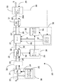
図1Aは、SONETネットワーク上で複数のサービスをトランスペアレントに伝送する本発明によるマッピング・システムを備えた例示的な伝送システムのブロック図を示す。簡略化するため、この図では、矢印で示したような単一方向の伝送だけを示す。
【0027】
信号S1,...Sj,...Snは、SONETネットワーク7を介して、2つのサイトAとBの間で伝送され、SONET信号Sとなる。ここで、nは、トリビュタリの数であり、jは、1つのトリビュタリのレンジである。信号S1〜Snは、連続フォーマットのディジタル信号であり、ノードAおよびBにおいてSONET信号Sのトリビュタリとして扱われる。また、各信号SjのレートをRjで表し、信号SのレートをRで表す。信号Sjは、同じタイプまたは異なるタイプのサービスを搬送することができる。各トリビュタリ・レシーバ1−1nは、それぞれの連続フォーマットの信号S1−Snのデータ・ビットを復元する。ノードAは、1つまたは複数のシンクロナイザ201−20nを備え、各シンクロナイザ20jは、相当するトリビュタリ信号Sjのデータ・ビットを適切なサイズのSONETエンベロープにマッピングする。
【0028】
いくつかの伝送ノード間で連続信号をトランスペアレントに搬送するフレームのサイズは、ソフトウェアで選択され、大きいレンジの連続フォーマットの信号に十分な帯域幅使用量を考慮して提供される。たとえば、エンベロープにnxSTS−12が使用される場合、nは、高速のシンクロナイザの場合は4〜20であり、中速のシンクロナイザの場合は1〜5である。これにより、大きいネットワーク容量が無駄になるのが防止される。
【0029】
各信号が、それぞれのSONETエンベロープ内にマップされた後、トリビュタリは、SONETマルチプレクサ3によって高レート信号Sに多重化され、それが、SONETトランスミッタ5によって光ネットワーク7を介してサイトBの方に送られる。
【0030】
逆の操作が、サイトBにおいて行われる。すなわち、光レシーバ9が、信号Sのデータを復元し、デマルチプレクサ3′がその信号を分離し、それを各デシンクロナイザ40−40nに提供する。各デシンクロナイザ40jは、トリビュタリ・トランスミッタ11jに提供される信号Sjと関連したそれぞれのフォーマットでビットを再配列する。各トリビュタリ・トランスミッタ11−11nは、各信号S1−Snを、関連したトリビュタリ・ネットワーク上に送り出すか、関連したエンド・ユーザに送り出す。
【0031】
次に、基礎的な概念と実現性を示すために、信号STS−192cについてマッピング・アルゴリズムの例を示す。他のエンベロープを使用することもでき、本発明は、信号STS−192cに制限されない。
【0032】
図1Bは、TOH2とSTS−192c SPE(同期ペイロード・エンベロープ)4を含むSTS−192cフレーム1を示す。ペイロードは、192×87×9×8=1,202,688ビットを含む。
【0033】
ここでは、ブロック10−jが、後で説明するようなデータ・ビット、固定スタッフ・ビットおよび適応スタッフ・ビットを含む1056ビット・フィールドとして定義される。STS−192 SPEは、灰色に示され参照番号8で示された領域を占める1138のブロック10−1〜10−K(ここで、K=1138)を収容することができる。ブロック・フィールド8は、1,201,728ビットを有する。エンベロープ4内の残りの960ビットは、POHビット6(9×8=72ビット)と、888ビットの剰余フィールド14からなる。フィールド6および14のビットの数は、SONETフレーム1内にマップされる連続フォーマットの信号のレートR1に関係なく不変である。したがって、これらのビットは、以下において固定スタッフ・ビットと呼ばれる。
【0034】
一方、ブロック・フィールド8を埋めるのに必要なスタッフ・ビットの数は、連続フォーマットの信号S1のレートR1の関数を変化させる。これらのスタッフ・ビットは、本明細書において、適応スタッフ・ビットと呼ばれる。
【0035】
本発明によれば、信号S1のデータ・ビットは、固定スタッフ・ビットと適応スタッフ・ビットが均等に分散されたフレーム1内にマッピングされる。そのようなスタッフ・ビットは、レートR1があらかじめ分からない場合があるため、実行中に、各ブロックに均等に分散される。したがって、シンクロナイザは、現行ブロックのデータ・ビットがマッピングされるときに蓄積された位相情報に基づいて、データ・ビットの場所である有効位置と、次のブロックのスタッフ・ビットの場所である無効位置を定義する。さらにまた、シンクロナイザは、実際のマッピング時にオーバヘッドを均等に分散させるが、マッピング動作後にそれをSONET規格に従って提供されるタイムスロットに再編成し、その結果、フレームがSONET装置によって認識される。遠端において、シンクロナイザは、固定スタッフ・ビットと適応スタッフ・ビットを吸収することによって逆の動作を行い、それによりデータ・ビットを逆マッピングしてS1を再生することができる。
【0036】
図1Bは、フレームの構造を直観的に示すが、本発明によれば、マッピング・アルゴリズムが、固定スタッフ・ビットと適応スタッフ・ビットをフレーム1内に均等に分散させることに注意されたい。以上の計算は、STS−192cフレームに適用することができるが、類似の事が他のSONET信号にも当てはまることに注意されたい。
【0037】
各ブロックのビットは、図1Cに示したように割り振られる。ブロック10−1は、データ用に1023(210−1)のビットを有するデータ・フィールド17と、16ビットを有する制御フィールド13と、将来使用するための17ビットを有するスペア・フィールド15とを含む。
【0038】
フィールド17の1023ビットは、データをSTS−192cフレーム内伝送するための9,313.392Mbps(1023×1138×8000)のビット・レートを提供する。フレームのサイズは、一定の用途のために提供され固定され、すなわち、任意のレートのトリビュタリが、同じサイズのフレームにマッピングされる。マッピング技術は、トリビュタリごとに異なるフレームが使用されるのではなく、任意のトリビュタリに適応する。トリビュタリが、9,313.392Mbpsより低いレートを有する場合は、トリビュタリをSTS−192cに合うように調整し、データ・フィールド8の多くのビットをスタッフ・ビットに変化させなければならない。図1Cは、フィールド17内の可変サイズvのフィールド19を示し、そのサイズは、マッピング中に、信号S1のクロックと信号Sのクロックの位相を比較することによって決定される。
【0039】
フィールド13は、10ビットの制御関数βを含む。βのサイズは、ブロックのサイズに従って、後で述べる適応スタッフィング・アルゴリズムにより次のブロック内の有効ビットの位置を一意に決定するように選択される。10ビットという数によって、1024個の値を想定することが可能であり、この数はブロックの有効ビットの数よりも1大きい。βの値は、また、次のブロックにおける有効ビットの数を与える。単一ビット誤り訂正と複数誤り検出には、フィールド13の追加の6ビットが必要である。
【0040】
複数誤り検出の場合、前のブロックからのβが、デフォルトとして、最小のPLL過渡事象でダウンストリームを高速でリフレームするのに使用される。フィールド15および19のビットは、ブロック内に分散される。
【0041】
すべてのブロックが同じ数の適応スタッフ・ビットを有するとは限らないので、βの値は、隣り合ったブロックで異なることがあるが、各ブロック内でβは一定のままである。
【0042】
適応スタッフィング・アルゴリズムは、αで表された、βと逆の2進ビットを定義する。すなわち、βの最上位ビットが、αの最下位ビットになり、 同様に、αの最下位ビットが、βの最上位ビットになる。表1は、この変換を例として示す。
【0043】
【表1】

αは、また、ブロックごとに決定され、βの場合と同じように、αの値は、隣り合ったブロック間では異なるが、ブロック内では変化しない。
【0045】
また、ここで、カウンタCと値Dが定義される。Cは、1ブロック内のビットのカウンタであり、10ビットの2進数によって表される。Cは、1から1023まで増加し、それによりブロック内のビットが占めるタイムスロットを識別する。
【0046】
Dは、Cのビット遷移デルタであり、ちょうど1つのビット・セットによる10ビット2進数によって表される。このセット・ビットは、カウンタCが1ビット進むときに生ずる0から1への遷移の位置にある。Dの各ビットは、ブール関数を使用して、次の式に従って、カウンタCのレンジnとn−1のビットによって与えられる。
【0047】
【数1】
Dn=Cn AND NOT(C−1)n
【0048】
表2は、所与の値Cに関してDがとる値の例を示す。
【0049】
【表2】
ブロックの有効データ間にスタッフ・ビットをある程度均一に分散させるために、本発明による適応スタッフィング・アルゴリズムは、Dにおけるビットがαにおいてもセットされるときにビットが有効であることを述べている。
【0051】
これは、ブロックのC番目のビットについて、次の式2のように示すことができる。
【0052】
【数2】
![]()
有効ビットは、データに割り当てられたビットに対応し、したがって無効ビットは、スタッフ・ビットに対応する。表3は、βのサイズが3ビットの場合に、アルゴリズムが7ビットのブロックにどのように機能するかの簡単な例を示す。アルゴリズムは、1023ビットと10ビットβのブロックに同じようにはたらくことが分かるが、本明細書では、完全なスタッフィング・シーケンスについて詳述することは実際的でない。
【0054】
表3の項目は、2進関数Valid(C,β)の結果である。列は、βで与えられたようなブロック内の特定数の有効ビットにデータ・ビットとスタッフ・ビットがどのように分散されているかを示す。
【0055】
Valid(C)が真の場合のCの各値に関して、有効データ・ビットが、Cで識別されるタイムスロット内にあり、Valid(C)の真でない各値に関して、スタッフ・ビットがタイムスロットに入れられる。この方式を使用することにより、無効スタッフィング・ビットが、フレーム全体にほぼ均一に広がる。
【0056】
【表3】
この例では、カウンタCは、1から7までカウントし、Dの値が、各列においてCのすべての値に関して求められる。次に、Dの各値は、Cの増加に伴い、αと比較される。また、Dのセット・ビットがαにおいてセットされる場合は、ブロック内の対応するC番目のビットがデータ・ビットになる。Dのセット・ビットがαにおいてセットされない場合、ブロック内の対応するC番目のビットはスタッフ・ビットになる。
【0058】
例としてビット・レートR1/Rが有効能力の5/7のブロックの場合は、βが2進数5(101)であり、βの逆数の2進ビットαも5(101)であることを意味する。ブロック内のデータ・ビットとスタッフ・ビットの順序は、列ごとのValid(C,5)と同じであり、次の通りである。
【0059】
Data,Stuff,Data,Data,Data,Stuff,Dataまた、表3に関して、Valid(C,5)の場合、5であるβは有効ビットの数でもあり、無効ビットがフレーム全体にほとんど均一に広がっていることは明らかである。
【0060】
図4および図5は、βがブロック間で少し異なる5つの連続ブロックのスタッフィング・シーケンスを連続して詳細に示す図である。図4および図5は、一点鎖線の部分においてつながる。この表において、カウンタCは、1から7までカウントし、2つの連続するブロックは、分かり易くするために異なる地色(灰色と白)で示されている。
【0061】
前に示したように、βは、各ブロックごとにセットされるが、スタッフ・ビットの総数とブロックの数の比が整数でない場合もあるため、次のブロックと異なることがある。次の例を検討する。
ブロック1(灰色)のβは5である。
ブロック2(黒)のβは6である。
ブロック3(灰色)のβは5である。
ブロック4(黒)のβは5である。
ブロック5(灰色)のβは6である。
【0062】
この場合、データ・ビット間のスタッフ・ビットの広がりは、図6に例示される通りである。ここで、Dはデータを表し、Sはスタッフを表す。上記のDとSの混乱を避けるために、これらは通常の文字で記述され、信号Sと、Cのビット遷移Dにはイタリック体が使用される。
【0063】
この場合も、図4および図5から、スタッフ・ビットが、βのわずかな変動があるものの、データ・ビット間にある程度均一に広がっていることが明らかである。
【0064】
図2は、トリビュタリ・シンクロナイザ20のブロック図を示す。任意のレートで受け取ったデータでSONET SPEを満たすことによって、前述のような透明性が得られる。データ経路は、幅の広い矢印および参照数字22と22′を使って示される。連続フォーマットおよびレートR1を有する信号S1が、データ・リカバリ・ユニット36によって検出される。次に、データ・ビットは、充填制御ボックス38、マッピング・ユニット30、レシーバ・オーバヘッドFIFO(先入れ先出し)31、およびオーバヘッド・マルチプレクサ33を通る。このとき、シンクロナイザ20から出力された信号は、SONETフレーム内にある。信号Sが、それぞれのOAM&P情報と供にSONET型オーバヘッド(TOHとPOH)を有し、同期ペイロード内へのビットの配置が、SONETの規格と異なるマッピング・アルゴリズムに従うことを理解されたい。
【0065】
シンクロナイザ20が、異なる4つのクロック、すなわちデータ・クロック24、ブロック・クロック26、マッピング・クロック32、ならびにSONETクロック28および28Aを操作する。クロック28は、STS−192のレートを有し、クロック28Aは、フレームのレートを有する。データ・クロック24(レートR1)は、レシーバ21とフレキシブル・クロック・リカバリ回路25を含むデータ・リカバリ・ユニット36によって入力データから復元される。フレキシブル・クロック・リカバリ回路25は、広い連続した範囲のビット・レートにわたるクロック・リカバリが可能である。そのような回路の例は、1998年12月22日に出願され、Northern Telecom Limitedに譲渡された、Habelらによる「Apparatus and Method for Versatile Digital Communication」と題する同時係属米国特許出願09/218053に開示されている。この出願は、参照により本明細書に組み込まれる。
【0066】
図2において点線で示したオフ・ライン・フレーマ39が、ある組の既知の信号フォーマットを認識することができ、フレームとBER性能情報が報告される。また、マッピング効率を高めるために、回線符号化をレシーバにおいていくつかの信号から除去し、トランスミッタにおいて加えることができる、これらのオプションは、特定タイプのサービスに依存し、したがってここではさらに詳しく考察しない。
【0067】
レシーバ・バッファ・ユニット38は、伸縮性記憶装置23とレシーバ・ディジタルPLL29を含む。データ・クロック24は、マッピング・クロック32の制御下で空にされる伸縮性記憶装置23へのデータの入力をクロックするために使用される。マッピング・クロック32は、STS−192クロック28から得られたギャップド・クロックである。このクロックは、ブロック・クロックにおけるギャップの他に、マッピング・アルゴリズムによって決定されるような適切な位相時に中断される。この方法において、データ22は、マッパ27の入力においてマッピング周波数と同期される。
【0068】
ペイロード・フィールド4に、データ・ビットが必要な容量まで連続的に満たされ、残りの容量がスタッフ・ビットの連続体である場合、伸縮性記憶装置23の容量は、幅広く変化することになり、記憶装置23にある程度大きい深さを必要とする。伸縮性記憶装置23は、スタッフ・ビットがロードされている間に急速に満たされ、トリビュタリ・データ・ビットの連続ストリームがロードされている間に急速に空になる。この状況は、図2の構成において回避され、この場合、伸縮性記憶装置23は、マッピング・クロック32によって実質的に規則正しい間隔で空にされる。
【0069】
一方、伸縮性記憶装置23は、トリビュタリからのすべての入力ジッタおよびワンダを十分に吸収できる深さでなければならない。伸縮性記憶装置23の充填が十分に制御されれば、最悪の場合のジッタとワンダが存在してもオーバーフローしたりアンダーフローしないことを保証することができ、またシンクロナイザ20は、ジッタの許容要件を満たす。伸縮性記憶装置23の最小サイズは、実験的に、256ビットで決定された。
【0070】
レシーバ・ディジタルPLL29は、マッピング・クロック32を決定するβによって最適な充填を維持するように伸縮性記憶装置を空にする割合を制御する。換言すると、マッピング・クロック32の平均レートは、データ・クロック24の平均レートをたどるように制御され、βは、それらのクロック間の位相差から得られる。前に示したように、βは、次のブロックの充填を制御する。この制御は、シンクロナイザ20がSONET規格に従うポインタの調整を必要としないという利点を有する。より正確に言うと、伸縮性記憶装置の充填の制御は、最大トリビュタリ・レートがペイロード・レートを超えない限り、時間によるラインおよびトリビュタリのレート変動(ラインおよびトリビュタリのジッタおよびワンダ)を改善する。
【0071】
βを決定するために、伸縮性記憶装置23への入力が、周期的にサンプリングされ、データ22の位相情報が、PLL29に入力される。たとえば、ディジタルPLL29は、24ビットのアキュムレータを含む。ブロックの最初に、マッパ27のカウンタCによって与えられた伸縮性記憶装置23の充填は、たとえば50%を基準としてラッチされる。次に、サンプル34の位相は、アキュムレータ内に加えられ、3ビットだけ左にシフトされた位相に加えられる。この和Sの上位10ビットは、βである。アキュムレータは、ロールオーバーしないようにFFFFFFでクリップされ、アナログ出力PLLレンジの低い周波制限を反映するために400000などの最も低い値でクリップされなければならない。その他のディジタルPLLの実施態様も可能である。
【0072】
伸縮性記憶装置23が満杯になり始めると、マッピング・クロック32の速度を高めることによって記憶装置を空にするようにβが増加される。同様に、記憶装置23が空になり始めると、記憶装置23が充填することができるようにβが減らされる。目標の充填率は、50%が好ましい。
【0073】
マッピング・ユニット30は、ブロック・クロック・ギャッパ37、マッピング・クロック・ギャッパ35およびマッパ27を含む。
【0074】
ブロック・クロック・ギャッパ37は、SONET TOHのギャップと規則的サイクルを特徴とするSTS−192クロック28を受け取る。クロック28は、前述の例において、42,432のギャップがフレーム全体に均一に広がった1SONETフレーム当たり1138(ブロック数)×1056(ブロック・サイズ)=1,201,728サイクルを有するブロック・クロック26を生成する。前に示したように、ブロック・クロック26のギャップは、サイズが3×9×8×192のSONETオーバヘッド、すなわち図1Bのフィールド2と、サイズが960の固定スタッフィング、すなわちフィールド6および14によるものである。ブロック・クロック26は、フィールド8におけるビットの全体の割振りを表す。換言すると、フレームのオーバヘッド・サイズがSONET規格に従う場合に、ブロック・クロック26は、TOHビット、POHビット、および固定スタッフ・ビットのための空間を維持するために約30づつのビットに切断される。
【0075】
マッピング・クロック・ギャッパ・ブロック35は、ブロック・クロックと同じレートを有するが、前述のように、すべての有効ビット位置におけるパルスによりβの制御下でさらにギャップが開けられ、レートR1とRの間の差に基づいて適応スタッフ・ビットを生じさせる。
【0076】
マッパ27は、マッピング・クロック32、ブロック・クロック26、および簡単にするために示していない他の補足的クロックを利用し、固定スタッフ・ビットと適応スタッフ・ビットの両方を使用してデータ22の位置を調整する。マッピング・クロック32を使用して、伸縮性記憶装置23からデータ・ビットがマッパにクロック・タイミングで引き出される。ブロック・クロック26を使用して、マッパ27から、データ・ビット、固定スタッフ・ビットおよび適応スタッフ・ビットがクロック・タイミングで引き出される。マッパ27は、本質的にメモリを持たず、伸縮性記憶装置23とFIFO31は、シンクロナイザのすべてのメモリを表す。
【0077】
データ、固定スタッフ・ビットおよび適応スタッフ・ビットを含むような参照数字22′で示されたマッパ27からの複数のビットは、SONETオーバヘッドの場所のためにタイムスロットを予約するレシーバ・オーバヘッドFIFO(先入れ先出し)31にクロック・タイミングで入れられる。次に、ビット22′は、クロック28Aによってクロック・タイミングでFIFO31から引き出され、それによりFIFO31は、各フレームごとに一度同期してリセットされる。FIFO31の深さは、フレームOHがOH MUXにクロック・タイミングで入れられているときにフレームの位相瞬間においてペイロード・ビットだけを記憶するのに十分であれば良い。フレームが、SONETと同じペイロード対OHの比を有する場合、この深さは、192×8×9×3ビットより大きくなければならず、192×8×12×3ビットよりも大きいことが好ましい。
【0078】
ビット22′は、FIFOブロック31から、SONETオーバヘッド・マルチプレクサ33にクロック・タイミングで入れられ、そこでSONETオーバヘッドが、それぞれ空のタイムスロットに加えられ、次に信号が、STS−192として処理される。細い線で示したSONETクロック28および28Aは、通常通り、シェルフの残りの部分に対してロックされる。
【0079】
簡単にするために、直列ハードウェア実装について説明する。バイト幅の実装のようなこの種のマッピングの並列実装により、クロック速度を低くすることができる。そのような並列実装は、ジッタを減少させるためにブロック・アライメントを交互にすることがあった。PLLを最適化するために、ハードウェア制御よりもDSP制御の方が大きな自由度を提供する。
【0080】
図3は、トランスペアレントな逆方向のシンクロナイザ、すなわちデシンクロナイザ40のトランスミッタ側のブロック図を示す。デシンクロナイザ40は、シンクロナイザ20によって実行されるのとは逆の機能を類似の方法で実行し、類似したブロックを備える。
【0081】
SONETオーバヘッド・デマルチプレクサ53は、シェルフの残りの部分に通常通りロックされるSTS−192クロック28を使用して、信号42′からSONETオーバヘッドを示す。トランスミッタ・オーバヘッドFIFO51は、各フレームごとに、クロック28Aと同期してリセットされる。オーバヘッドFIFO51は、データ・ビットを固定スタッフ・ビットおよび適応スタッフ・ビットと一緒に含むペーロードに受け取ったデータ42′をマッパ47に提供するようにオーバヘッド位置を吸収する。
【0082】
ポインタの位置調整を考慮しない場合、トランスミッタOH FIFO51は、シンクロナイザ20のレシーバOH FIFO31と類似の深さを有することがある。たとえば、SONET OHがフレームに使用される場合、必要な深さは、FIFO31の場合と同じように、192×8×12×3ビットである。したがって、FIFOは、OHがビット・ストリームから多重分離されるフレーム段階の間にトランスミッタOH FIFO51が空にならないように十分なデータ・ビットを記憶することができる。しかしながら、デシンクロナイザにポインタ・アライメントが必要であるため、トランスミッタOH FIFO51は、最悪の場合の一連の正または負のポインタ調整イベントを許容するように深さを大きくしなければならない。
【0083】
逆マッピング・ユニット50は、逆マッパ47、マッピング・クロック・ギャッパ55、およびブロック・クロック・ギャッパ57を含む。
【0084】
ブロック・クロック・ギャッパ57は、STS−192クロック28のギャップを調整してブロック・クロック26を作成する。ブロック・クロック26は、シンクロナイザ20の場合と同じように、1フレーム当たり1,201,728のサイクルを有し、フレーム全体に42,432のギャップが均一に広がる。ギャップは、図1Bのフィールド2、6および14に相当する。換言すると、このクロックは、TOHと固定スタッフ・ビットを拒否する。
【0085】
デシンクロナイザのブロック・クロック・ギャッパ57は、また、ポインタ調整のためにギャップを含めたり削除したりする。そのようなギャップは、ポインタ調整による位相ヒットを最少にするために3つのフレームに広げなければならない。
【0086】
マッピング・クロック・ギャッパ55は、ブロック内のインバンドOHチャネルから読み取ったブロック・クロック26およびβを受け取る。ギャップド・クロック26は、βを使用して、マッピング・クロック32を生成するようにさらにギャップが調整される。マッピング・クロック32は、厳密にトリビュタリ・データ・ビット42がクロック・タイミングで取り出されるようにデータ・ビット42′をギャップ・タイミングで取り出す。
【0087】
ビット42は、次に、伸縮性記憶装置43とトランスミッタ・ディジタルPLL49を含むトランスミッタ・バッファ・ユニット54によって処理される。トリビュタリ・データ・ビット42は、マッピング・クロック32を使用して出力伸縮性記憶装置43にクロック・タイミングで入れられる。伸縮性記憶装置43は、フレキシブル・クロック・リカバリ回路45から出力されたデータ・クロック24によって空にされる。
【0088】
出力伸縮性記憶装置43の位相は、トランスミッタ・ディジタルPLLによって周期的にサンプリングされる。サンプル34は、ディジタル的に処理され、出力信号がフレキシブル・クロック45に渡され、VCOの電圧が制御される。フレキシブル・クロック回路45は、シンクロナイザのフレキシブル・クロック回路25を備えた類似のタイプであり、データ・クロック24を提供する。
【0089】
TxPLL49の帯域幅は、マッピングとポインタ調整によるジッタをフィルタリングできるほど低く、またVCO雑音を抑制できるほど高くなければならない。
【0090】
本発明を、特定の実施形態の例に関して説明したが、本発明の意図から逸脱することなくその広い態様において、併記の特許請求の範囲内で当業者が想起するさらに他の修正および改良を行うことができる。
【図面の簡単な説明】
【図1】 本発明を例示する図であり、図1Aは本発明によるマッピング・システムを備えた通信ネットワークのブロック図である。図1Bは本発明の実施形態によるブロックを示すOC−192cフレームの図である。図1Cはブロックの構造の例を示す図である。
【図2】 本発明の実施形態によるシンクロナイザのブロック図である。
【図3】 本発明の実施形態によるデシンクロナイザのブロック図である。
【図4】 適応スタッフィング・アルゴリズムを例示する表を示す図である。
【図5】 図5に続く、適応スタッフィング・アルゴリズムを例示する表を示す図である。
【図6】 スタッフ・ビットの広がりを例示する図である。
【符号の説明】
20 シンクロナイザ
21 レシーバ
22 データ
23 伸縮性記憶装置
24 データ・クロック
25 フレキシブル・クロック・リカバリ回路
26 ギャップド・クロック
27 マッパ
28 STS−192クロック
30 マッピング・ユニット
31 FIFO
32 マッピング・クロック
33 オーバヘッド・マルチプレクサ
34 サンプル
35 マッピング・クロック・ギャッパ・ブロック
36 データ・リカバリ・ユニット
37 ブロック・クロック・ギャッパ
38 レシーバ・バッファ・ユニット
39 オフ・ライン・フレーマ[0001]
BACKGROUND OF THE INVENTION
The present invention is directed to transparent (transparent) transmission of a data signal having a continuous format, and in particular to a method for mapping an arbitrary continuous signal in a SONET frame.
[0002]
[Prior art]
Providing the services requested by customers quickly is an important function of the network. The range of bit rates for such services can be large, and in fact the services and their bit rates may not be defined when a network device is introduced. Therefore, providing an arbitrary bit rate service quickly is an important function.
[0003]
Data transmission formats can be divided into SONET and other continuous formats and burst formats. Burst formats do not have a continuous clock, and transmission of such signals does not require a predetermined phase relationship between bursts. On the other hand, the clock phase of the continuous format has continuity in the normal state, and the frequency of the clock is limited. Examples of such limits are ± 20 ppm (parts per million) and ± 100 ppm.
[0004]
The mainstream signal format in fiber optic networks follows the synchronization standard SONET in North America and SDH in other regions. In this specification, SONET is defined to include SDH. SONET enables signal multiplexing, adding and dropping, and general transmission. With regard to services, being able to be easily transmitted by a SONET network is an important characteristic in that it allows a network provider to use a large foundation of installed SONET compatible devices.
[0005]
SONET is a physical transport technology that can provide transmission services such as ATM, SMDS, frame relay, T1, and E1. SONET operation, management, maintenance and provisioning (OAM & P) functions can also reduce the amount of back-to-back multiplexing, and more importantly, network providers can Operating costs can be reduced.
[0006]
The SONET standards ANSI T1.105 and Bellcore GR-253-CORE define a physical interface, an optical line rate known as an optical signal carrier (OC), a frame format, and an OAM & P protocol. Optical / electrical conversion takes place at the periphery of the SONET network, where the optical signal is converted into a standard electrical format called Synchronous Transmission Signal (STS) which is the equivalent of the optical signal. That is, the STS signal is carried by each optical carrier defined according to the carrying STS. Thus, signal STS-192 is carried by optical signal OC-192.
[0007]
The STS-1 frame is composed of 90 columns × 9 rows of bytes, and the frame length is 125 microseconds. The frame includes a transmission overhead (TOH) occupying 3 columns × 9 rows of bytes and a synchronous payload envelope (SPE) occupying 87 columns × 9 rows of bytes. The first column of the SPE is occupied by path overhead bytes.
[0008]
Therefore, STS-1 has a bit rate of 51.840 Mb / sec. The lower rate is a subset of STS-1 and is known as Virtual Tributary (VT), which may transmit at a lower rate than DS3. The higher rate STS-N is constructed by multiplexing the lower rate tributaries using a SONET add / drop multiplexer. Here, N = 1, 3, 12,. . . 192 or higher. The signal STS-N is obtained by interleaving N STS-1 signals. For example, STS-192 consists of 192 STS-1 tributaries that each look different and are arranged separately in the envelope. Individual tributaries can carry different payloads, each with a different destination.
[0009]
The STS-N has a TOH consisting of N TOHs in total for each tributary, and a SPE consisting of N SPEs in total for the tributaries, each having its own POH (path overhead).
[0010]
Some services that operate at higher speeds are transmitted on the STS-Nc signal (concatenation c). STS-1 is maintained together in the STS-Nc signal. The entire envelope of the STS-Nc signal is routed, multiplexed and transmitted as a single entry rather than as N separate entries. The TOH for the N component and the beginning of the SPE are all matched to the lock as all components are generated by the same source. The first STS-1 in the continuous signal carries a set of POH required for STS-Nc.
[0011]
Methods for mapping one rate or format to another rate or format are well known. Bellcore TR-0253 describes in detail the standard mapping of common asynchronous transmission formats (DS0, DS1, DS2, DS3, etc.) to SONET. A similar mapping is defined for ETSI hierarchical mapping to SDH. An optical transmission device maps one unique format to another. For example, FD-565 can carry Nortel's proprietary format FD-135 as well as the standard format DS3.
[0012]
However, standard or proprietary mechanisms allow the transmission of a very specific set of signals with format-specific hardware. Such a mapping method cannot be used to map rates that differ significantly from the standard. Further, each such mapping is precisely adjusted with a tolerance of, for example, ± 20 ppm for a particular format and a particular bit rate. A signal cannot be transmitted in SONET if it has a bit rate that is even 1% different from DS3, for example. Furthermore, different hardware units are generally required to perform various signal mappings.
[0013]
The solution to the aforementioned problem is to add a “wrapper” to any continuous signal. The resulting signal rate is a function of the signal being wrapped. That is, when a 1 Mb / sec wrapper is added to a rate X signal, a format having a rate X + 1 Mb / sec is generated. This change increases the proportion of X. For example, the common channel coding 8B / 10B creates a format having a rate of 112.5% of X. Thus, the “wrapper” method does not generate a format with a predefined constant bit rate for any input. In general, the obtained signal cannot be time-division multiplexed and transmitted over a high-speed network.
[0014]
[Problems to be solved by the invention]
US Pat. No. 5,784,594 (Beatty) proposes a “TDM wrapper” format in which an arbitrary signal is mapped to the required number of frames and the remaining frames are left empty. However, this method requires a very large memory per translation direction to hold the bits while waiting for the appropriate time slot to send the bits. As a result, this format is expensive to implement with high-speed signals.
[0015]
The packet or cell based format maps any input stream to SONET and SDH. These methods are suitable for packet systems, but do not meet the jitter and wander requirements of most continuous signal formats because a “one size fits all” mapping method is used. The clock phase information of the input signal is completely deleted in such a way and can therefore not be transmitted.
[0016]
US patent application Ser. No. 09 / 307,812 (application entitled “Protocol Independent sub-rate device”, filed May 10, 1999 and assigned to Nortel Networks Corporation by Solheim et al.) Is a different type of client (IP, ATM , SONET, Ethernet, etc.). The application discloses a method of time division multiplexing a slow (sub-rate) channel of any rate and format into a single fast channel and then demultiplexing the channel at the far end of the system. The portion of bandwidth allocated to any given subrate channel can be provided without changes to hardware or software. This greatly facilitates and speeds up the provision of such services by the carrier. Tributaries with new protocols can also be addressed, and sending for support of such new protocols is greatly accelerated.
[0017]
There remains a need for an efficient method and apparatus for mapping arbitrary signals to SONET so that the signal can be recovered with low timing jitter and low cost.
[0018]
[Means for Solving the Problems]
An object of the present invention is to map any signal having a continuous format within a SONET frame. As a result, any format that meets the standard can be transmitted transparently within the SONET network.
[0019]
Therefore, the present invention transmits a continuous digital signal having an arbitrary rate R1 as a transparent tributary through a synchronous network, selects a fixed-length container signal having a rate R higher than the arbitrary rate R1 of the continuous signal, and transmits the transmission site. In which the bits of the continuous signal are distributed in the valid time slots of the frame of the container signal and the stuff bits are provided in the invalid time slots evenly distributed in the frame.
[0020]
The present invention further accepts a continuous format signal to map a stream of data bits and an arbitrary stream to map a continuous format signal of any rate for transmission as a transparent tributary signal over a synchronous network. A data recovery unit that recovers the data clock indicating the rate; a receiver that receives a stream of data bits, determines the phase difference between an arbitrary rate and the rate of the tributary frame, and generates a control function β Retrieves a stream of data bits from the buffer unit and the receiver buffer unit at the mapping clock rate, and evenly counts the stuff bits and data bits in the frame at the block clock rate according to the control function β Distributed Including a synchronizer including a mapping unit.
[0021]
According to another aspect of the present invention, a tributary frame is received at a block clock rate to demap a continuous format signal of any rate received as a transparent tributary signal over a synchronous network; An inverse mapping unit that receives the control function β and retrieves a stream of data bits at the mapping clock rate, while excluding stuff bits according to the control function β, and receives the data bits, and an arbitrary rate and frame rate A desynchronizer is provided that includes a transmitter buffer unit that determines a phase difference between and a data transmission unit that receives data bits and transmits a continuous format signal at a data rate controlled by the phase difference.
[0022]
The method of mapping according to the present invention is advantageous because it enables general techniques such as SONET to be used for transparent transmission of the same or different types of tributaries. By using this new mapping, almost all continuous formats can be transmitted without changing bits. Another advantage of the present invention is that the jitter or wander added by this method is minimal.
[0023]
The synchronizer / de-synchronizer according to the present invention processes signals whose format is not known at the design as long as the jitter tolerance and generation specifications are compatible with the very high capacity range designed in the unit. This is a unique mapping designed on the fly by the tributary software and sent in the channel to the corresponding tributary at the far end.
[0024]
These and other objects, features and advantages of the present invention will become apparent from the following more specific description of the preferred embodiment as illustrated in the accompanying drawings.
[0025]
DETAILED DESCRIPTION OF THE INVENTION
The mapping system according to the present invention maps a digital signal having a constant line speed below a specified maximum capacity into a SONET envelope of a provided size. The mapping function can be performed at the tributary unit of the SONET transmission shelf, and the reverse mapping function (also called demapping) can be performed at a similar unit at the far end of the SONET connection.
[0026]
FIG. 1A shows a block diagram of an exemplary transmission system with a mapping system according to the present invention for transparently transmitting multiple services over a SONET network. For simplicity, this figure shows only unidirectional transmissions as indicated by the arrows.
[0027]
The signals S1,... Sj,... Sn are transmitted between the two sites A and B via the
[0028]
The size of the frame that carries the continuous signal transparently between several transmission nodes is selected by software and provided with sufficient bandwidth usage for a large range of continuous format signals. For example, when nxSTS-12 is used for the envelope, n is 4 to 20 for a high speed synchronizer and 1 to 5 for a medium speed synchronizer. This prevents a large network capacity from being wasted.
[0029]
After each signal is mapped into its respective SONET envelope, the tributary is multiplexed into the high rate signal S by the
[0030]
The reverse operation is performed at site B. That is, the
[0031]
Next, in order to show the basic concept and feasibility, an example of a mapping algorithm is shown for signal STS-192c. Other envelopes can be used and the invention is not limited to signal STS-192c.
[0032]
FIG. 1B shows STS-
[0033]
Here, block 10-j is defined as a 1056 bit field containing data bits, fixed stuff bits and adaptive stuff bits as described below. The STS-192 SPE can accommodate 1138 blocks 10-1 to 10-K (where K = 1138) that are gray and occupy the area indicated by
[0034]
On the other hand, the number of stuff bits required to fill the
[0035]
According to the invention, the data bits of the signal S1 are mapped in a
[0036]
Although FIG. 1B intuitively shows the structure of the frame, it should be noted that, according to the present invention, the mapping algorithm distributes the fixed stuff bits and adaptive stuff bits evenly in
[0037]
The bits of each block are allocated as shown in FIG. 1C. Block 10-1 uses 1023 (2 Ten -1) includes a
[0038]
The 1023 bits in
[0039]
[0040]
In the case of multiple error detection, β from the previous block is used by default to fast reframe the downstream with minimal PLL transients. The bits of
[0041]
Since not all blocks have the same number of adaptive stuff bits, the value of β may be different in adjacent blocks, but β remains constant within each block.
[0042]
The adaptive stuffing algorithm defines a binary bit, denoted α, that is the opposite of β. That is, the most significant bit of β becomes the least significant bit of α, and similarly, the least significant bit of α becomes the most significant bit of β. Table 1 shows this conversion as an example.
[0043]
[Table 1]
α is also determined for each block, and as in β, the value of α differs between adjacent blocks, but does not change within a block.
[0045]
Here, a counter C and a value D are defined. C is a counter of bits in one block, and is represented by a 10-bit binary number. C increases from 1 to 1023, thereby identifying the time slot occupied by the bits in the block.
[0046]
D is the bit transition delta of C and is represented by a 10-bit binary number with exactly one bit set. This set bit is at the 0 to 1 transition that occurs when the counter C advances one bit. Each bit of D is given by the range n and n-1 bits of counter C according to the following equation using a Boolean function:
[0047]
[Expression 1]
Dn = Cn AND NOT (C-1) n
[0048]
Table 2 shows examples of values that D takes for a given value C.
[0049]
[Table 2]
In order to distribute the stuff bits to some extent evenly between the valid data of the blocks, the adaptive stuffing algorithm according to the invention states that the bits are valid when the bits in D are also set in α.
[0051]
This can be shown for the Cth bit of the block as in
[0052]
[Expression 2]
![]()
Valid bits correspond to bits assigned to the data, and therefore invalid bits correspond to stuff bits. Table 3 shows a simple example of how the algorithm works for a 7-bit block when the size of β is 3 bits. Although it can be seen that the algorithm works equally well for the 1023 bit and 10 bit β blocks, it is not practical to elaborate on the complete stuffing sequence here.
[0054]
The items in Table 3 are the results of the binary function Valid (C, β). The column shows how the data bits and stuff bits are distributed over a specific number of significant bits in the block as given by β.
[0055]
For each value of C when Valid (C) is true, a valid data bit is in the time slot identified by C, and for each value of Valid (C) that is not true, the stuff bit is in the time slot. Can be put. By using this scheme, invalid stuffing bits are spread almost uniformly throughout the frame.
[0056]
[Table 3]
In this example, counter C counts from 1 to 7, and the value of D is determined for all values of C in each column. Next, each value of D is compared with α as C increases. Also, if the set bit of D is set at α, the corresponding Cth bit in the block becomes the data bit. If the set bit of D is not set at α, the corresponding Cth bit in the block becomes a stuff bit.
[0058]
For example, if the bit rate R1 / R is a 5/7 block with effective capacity, β is a binary number 5 (101), and the binary bit α that is the inverse of β is also 5 (101). To do. The order of data bits and stuff bits in the block is the same as Valid (C, 5) for each column, and is as follows.
[0059]
Data, Stuff, Data, Data, Data, Stuff, Data Also, with respect to Table 3, in the case of Valid (C, 5), β which is 5 is also the number of valid bits, and invalid bits spread almost uniformly throughout the frame. It is clear that
[0060]
FIG. 4 and FIG. 5 are diagrams showing in detail a stuffing sequence of five consecutive blocks in which β is slightly different between blocks. 4 and 5 are connected at a portion indicated by a one-dot chain line. In this table, counter C counts from 1 to 7, and two consecutive blocks are shown in different ground colors (gray and white) for clarity.
[0061]
As previously indicated, β is set for each block, but may differ from the next block because the ratio of the total number of stuff bits to the number of blocks may not be an integer. Consider the following example:
Β of block 1 (gray) is 5.
Β in block 2 (black) is 6.
Β in block 3 (gray) is 5.
In block 4 (black), β is 5.
Β in block 5 (gray) is 6.
[0062]
In this case, the spread of the stuff bits between the data bits is as illustrated in FIG. Here, D represents data, and S represents staff. In order to avoid the confusion of D and S described above, these are written in ordinary characters, and italicized font is used for the signal S and the bit transition D of C.
[0063]
Again, it is clear from FIGS. 4 and 5 that the stuff bits are spread out evenly between the data bits, although there is a slight variation in β.
[0064]
FIG. 2 shows a block diagram of the
[0065]
The
[0066]
An off-
[0067]
The
[0068]
If the
[0069]
On the other hand, the
[0070]
The receiver
[0071]
In order to determine β, the input to the
[0072]
As the
[0073]
The
[0074]
The
[0075]
The mapping
[0076]
[0077]
A plurality of bits from the
[0078]
Bit 22 'is clocked from the
[0079]
For simplicity, a serial hardware implementation is described. A parallel implementation of this kind of mapping, such as a byte-wide implementation, can reduce the clock speed. Such a parallel implementation may alternate block alignment to reduce jitter. In order to optimize the PLL, DSP control provides greater freedom than hardware control.
[0080]
FIG. 3 shows a block diagram of the transmitter side of a transparent reverse synchronizer or
[0081]
The SONET
[0082]
Without considering pointer alignment, the
[0083]
The
[0084]
The
[0085]
The desynchronizer
[0086]
The
[0087]
[0088]
The phase of the
[0089]
The bandwidth of the
[0090]
While the invention has been described in terms of specific embodiments, further modifications and improvements will occur to those skilled in the art within the broad scope of the appended claims without departing from the spirit of the invention. be able to.
[Brief description of the drawings]
FIG. 1 is a diagram illustrating the present invention, and FIG. 1A is a block diagram of a communication network equipped with a mapping system according to the present invention. FIG. 1B is an OC-192c frame diagram illustrating blocks according to an embodiment of the present invention. FIG. 1C is a diagram illustrating an example of a block structure.
FIG. 2 is a block diagram of a synchronizer according to an embodiment of the present invention.
FIG. 3 is a block diagram of a desynchronizer according to an embodiment of the present invention.
FIG. 4 is a table illustrating an adaptive stuffing algorithm.
FIG. 5 is a table illustrating an adaptive stuffing algorithm following FIG. 5;
FIG. 6 is a diagram illustrating the spread of stuff bits.
[Explanation of symbols]
20 Synchronizer
21 Receiver
22 data
23 Elastic memory device
24 data clock
25 Flexible clock recovery circuit
26 Gapped Clock
27 Mapper
28 STS-192 clock
30 mapping units
31 FIFO
32 Mapping clock
33 Overhead multiplexer
34 samples
35 Mapping Clock Gapper Block
36 Data Recovery Unit
37 block clock gapper
38 Receiver buffer unit
39 Off-line framer
Claims (18)
前記連続信号の前記任意のレートR1よりも高いレートRの固定長コンテナ信号を選択する段階と、
送信サイトで、前記連続ディジタル信号のビットを前記コンテナ信号のフレームの有効タイムスロットに分散させ、前記フレームに均一に分散された無効タイムスロットにスタッフ・ビットを提供する段階と、を含み、
前記無効タイムスロットは、固定スタッフ・ビットおよび適応スタッフ・ビットの一方を含み、
前記提供する段階は、
データ・ビットの連続ストリームを受け取り、前記任意のレートR1と前記レートRの位相差を決定する段階と、
前記位相差に基づいて、前記連続ストリームに、前記フレーム内に前記固定スタッフ・ビットを収容するための一定の数のタイムスロットおよび前記フレーム内に前記適応スタッフ・ビットを収容するための調整可能な数のタイムスロットを加える段階と、
を含む送信方法。A method of transmitting a continuous digital signal of any rate R1 as a transparent tributary over a synchronous network, comprising:
Selecting a fixed-length container signal with a rate R higher than the arbitrary rate R1 of the continuous signal;
Distributing at the transmission site the bits of the continuous digital signal into valid time slots of a frame of the container signal and providing stuff bits in invalid time slots evenly distributed in the frame ;
The invalid time slot includes one of a fixed stuff bit and an adaptive stuff bit;
The providing step comprises:
Receiving a continuous stream of data bits and determining a phase difference between the arbitrary rate R1 and the rate R;
Based on the phase difference, the continuous stream is adjustable to accommodate a fixed number of time slots for accommodating the fixed stuff bits in the frame and the adaptive stuff bits in the frame. Adding a number of time slots,
Including sending method.
前記フレームを、いくつかの等しいサイズのデータ・ブロックと、前記一定の数のタイムスロットに分割する段階と、
各ブロックごとに、
固定スタッフ・ビットの数を決定し、前記ブロック内に前記固定スタッフ・ビットを均一に分散させる段階と、
前記調整可能な数を示す制御関数βを決定する段階と、
前記制御関数に基づいて前記固定スタッフ・ビットと前記適応スタッフ・ビットを次のブロック内に均一にマッピングする段階と、
を含む請求項1に記載の送信方法。Said adding step comprises
Dividing the frame into a number of equally sized data blocks and the fixed number of time slots;
For each block,
Determining the number of fixed stuff bits and uniformly distributing the fixed stuff bits within the block;
Determining a control function β indicative of the adjustable number;
Uniformly mapping the fixed stuff bits and the adaptive stuff bits into a next block based on the control function;
The transmission method according to claim 1, comprising:
前記ブロック内のタイムスロットを識別するカウンタCを提供する段階と、
前記制御関数βの逆の2進ビットαを定義する段階と、
前記カウンタCのビット遷移デルタを計算する段階と、
関数Valid(C,β)が偽のときに、前記カウンタCによって識別されるタイムスロットが無効タイムスロットであるかどうかを決定する段階と、
適応スタッフ・ビットを前記無効タイムスロット内に提供する段階と、
を含む請求項8に記載の送信方法。The mapping step comprises:
Providing a counter C identifying time slots within the block;
Defining an inverse binary bit α of the control function β;
Calculating a bit transition delta of the counter C;
Determining whether the time slot identified by the counter C is an invalid time slot when the function Valid (C, β) is false;
Providing an adaptation stuff bit in the invalid time slot;
The transmission method according to claim 8 , comprising:
前記連続フォーマットの信号を受け取り、データ・ビットのストリームと前記任意のレートを示すデータ・クロックとを復元するデータ・リカバリ・ユニットと、
前記データ・ビットのストリームを受け取り、前記任意のレートと前記トリビュタリのフレームのレートとの位相差を決定し、制御関数βを生成するレシーバ・バッファ・ユニットと、
前記レシーバ・バッファ・ユニットから前記データ・ビット・ストリームをマッピング・クロック・レートで取り出し、スタッフ・ビットとデータ・ビットのカウントを、前記制御関数βにしたがってブロック・クロック・レートで前記フレーム内に一様に分散させるマッピング・ユニットと、
を含むシンクロナイザ。A synchronizer that maps a continuous format signal of any rate for transmission as a transparent tributary signal over a synchronous network,
A data recovery unit that receives the continuous format signal and recovers a stream of data bits and a data clock indicative of the arbitrary rate;
A receiver buffer unit that receives the stream of data bits, determines a phase difference between the arbitrary rate and the rate of the tributary frame, and generates a control function β;
The data bit stream is extracted from the receiver buffer unit at a mapping clock rate, and a stuff bit and data bit count is counted in the frame at a block clock rate according to the control function β. Mapping units to be distributed like
Synchronizer including
ある量の前記ストリームのデータ・ビットを前記データ・クロックで一時的に記憶し、前記データ・ビットを前記ブロック・クロック・レートで前記マッピング・ユニットに提供する伸縮性記憶装置と、
前記任意のレートと前記マッピング・クロックとの位相差を決定し、前記制御関数βを提供するディジタルPLLと、
を含む請求項11に記載のシンクロナイザ。The receiver buffer unit is
A stretchable storage device that temporarily stores an amount of data bits of the stream at the data clock and provides the data bits to the mapping unit at the block clock rate;
A digital PLL that determines the phase difference between the arbitrary rate and the mapping clock and provides the control function β;
The synchronizer of Claim 11 containing.
前記同期フレームのレートを示すクロックを受け取り、前記同期フレームのすべてのタイムスロットを与えるブロック・レートの前記ブロック・クロック、および固定スタッフ・ビットを収容する一定の数のタイムスロットを与えるギャップを提供するブロック・クロック・ギャッパと、
前記ブロック・クロックと前記制御信号βを受け取り、前記同期フレームのすべてのタイムスロットを与えるマッピング・レートのマッピング・クロック、および前記フレーム内の適応スタッフ・ビットを収容する調整可能な数のタイムスロットを与えるギャップを提供するマッピング・クロック・ギャッパと、
前記ブロック・クロックと前記マッピング・クロックを受け取り、それに従って前記フレーム内の前記データ・ビットのストリームをマッピングするマッパと、
を含む請求項11に記載のシンクロナイザ。The mapping unit is
Receiving a clock indicative of the rate of the synchronization frame, providing a block rate of the block clock that gives all the time slots of the synchronization frame, and a gap giving a certain number of time slots to accommodate fixed stuff bits Block clock gapper,
A mapping rate mapping clock that receives the block clock and the control signal β and gives all time slots of the synchronization frame; and an adjustable number of time slots that accommodates adaptive stuff bits in the frame A mapping clock gapper that provides a gap to be given,
A mapper that receives the block clock and the mapping clock and maps the stream of data bits in the frame accordingly;
The synchronizer of Claim 11 containing.
ブロック・クロック・レートで前記トリビュタリのフレームを受け取り、制御関数βを受け取り、データ・ビットのストリームをマッピング・クロック・レートで取り出す一方、前記制御関数βに従ってスタッフ・ビットを除外する逆マッピング・ユニットと、
前記データ・ビットを受け取り、前記任意のレートと前記フレームのレートとの位相差を決定するトランスミッタ・バッファ・ユニットと、
前記データ・ビットを受け取り、前記位相差によって制御されたデータ・レートで前記連続フォーマットの信号を送信するためのデータ送信ユニットと、
を含むデシンクロナイザ。A de-synchronizer that reverse maps a continuous format signal of arbitrary rate received over a synchronous network as a transparent tributary,
An inverse mapping unit that receives the tributary frame at a block clock rate, receives a control function β, retrieves a stream of data bits at a mapping clock rate, and excludes stuff bits according to the control function β; ,
A transmitter buffer unit that receives the data bits and determines a phase difference between the arbitrary rate and the rate of the frame;
A data transmission unit for receiving the data bits and transmitting the signal in the continuous format at a data rate controlled by the phase difference;
Desynchronizer including
Applications Claiming Priority (2)
| Application Number | Priority Date | Filing Date | Title |
|---|---|---|---|
| US09/349087 | 1999-07-08 | ||
| US09/349,087 US7002986B1 (en) | 1999-07-08 | 1999-07-08 | Mapping arbitrary signals into SONET |
Publications (2)
| Publication Number | Publication Date |
|---|---|
| JP2001069104A JP2001069104A (en) | 2001-03-16 |
| JP4530385B2 true JP4530385B2 (en) | 2010-08-25 |
Family
ID=23370856
Family Applications (1)
| Application Number | Title | Priority Date | Filing Date |
|---|---|---|---|
| JP2000204447A Expired - Fee Related JP4530385B2 (en) | 1999-07-08 | 2000-07-06 | Method of mapping an arbitrary signal to SONET |
Country Status (5)
| Country | Link |
|---|---|
| US (3) | US7002986B1 (en) |
| EP (1) | EP1067722B1 (en) |
| JP (1) | JP4530385B2 (en) |
| CA (1) | CA2308968C (en) |
| DE (1) | DE60035926T2 (en) |
Families Citing this family (56)
| Publication number | Priority date | Publication date | Assignee | Title |
|---|---|---|---|---|
| US6522671B1 (en) * | 1999-05-10 | 2003-02-18 | Nortel Networks Limited | Protocol independent sub-rate device |
| US7002986B1 (en) * | 1999-07-08 | 2006-02-21 | Nortel Networks Limited | Mapping arbitrary signals into SONET |
| US7173930B2 (en) * | 1999-10-26 | 2007-02-06 | Ciena Corporation | Transparent flexible concatenation |
| US6937614B1 (en) * | 1999-11-12 | 2005-08-30 | Nortel Networks Limited | Transparent port for high rate networking |
| US7139743B2 (en) | 2000-04-07 | 2006-11-21 | Washington University | Associative database scanning and information retrieval using FPGA devices |
| US6711558B1 (en) | 2000-04-07 | 2004-03-23 | Washington University | Associative database scanning and information retrieval |
| US6870860B1 (en) * | 2000-04-19 | 2005-03-22 | Ciena Corporation | Semi-transparent time division multiplexer/demultiplexer |
| KR100358382B1 (en) * | 2000-08-28 | 2002-10-25 | 엘지전자 주식회사 | Apparatus for parallel mapping of serial input data in SDH system |
| US20020110157A1 (en) * | 2001-02-14 | 2002-08-15 | Kestrel Solutions | Method and apparatus for providing a gigabit ethernet circuit pack |
| US6816509B2 (en) * | 2001-03-02 | 2004-11-09 | Ciena Corporation | Data mapper and method for flexible mapping of control and data information within a SONET payload |
| JP3570507B2 (en) * | 2001-03-28 | 2004-09-29 | 日本電気株式会社 | STM mapping circuit and method |
| ITMI20010726A1 (en) * | 2001-04-05 | 2002-10-05 | Cit Alcatel | METHOD AND APPARATUS TO MAP FAST ETHERNET DATA INTERFACES IN A SINGLE VC-4 VIRTUAL CONTAINER OF A STM-1 / OC-3 PAYLOAD TRANSMITTED IN U |
| EP1396105B1 (en) * | 2001-04-26 | 2005-03-09 | International Business Machines Corporation | Multiple low-speed into single high-speed sdh/sonet channel mapper / framer device and method |
| EP1267507B1 (en) * | 2001-06-15 | 2005-02-02 | Lucent Technologies Inc. | A method and apparatus for transmitting and receiving multiplex tributary signals |
| US20030048813A1 (en) * | 2001-09-05 | 2003-03-13 | Optix Networks Inc. | Method for mapping and multiplexing constant bit rate signals into an optical transport network frame |
| US7023942B1 (en) * | 2001-10-09 | 2006-04-04 | Nortel Networks Limited | Method and apparatus for digital data synchronization |
| US7716330B2 (en) * | 2001-10-19 | 2010-05-11 | Global Velocity, Inc. | System and method for controlling transmission of data packets over an information network |
| WO2003043240A1 (en) * | 2001-11-13 | 2003-05-22 | Fujitsu Limited | Virtual concatenation transmission method and device |
| US7227876B1 (en) * | 2002-01-28 | 2007-06-05 | Pmc-Sierra, Inc. | FIFO buffer depth estimation for asynchronous gapped payloads |
| US20030185248A1 (en) * | 2002-03-27 | 2003-10-02 | Adc Telecommunications Israel Ltd. | Simplified bandwidth handling for SDH/SONET access rings |
| US20030225802A1 (en) * | 2002-06-02 | 2003-12-04 | Eci Telecom Ltd. | Enable generator EG, and method of mapping data using the EG |
| IL150011A (en) * | 2002-06-04 | 2007-12-03 | Eci Telecom Ltd | Mapping data in a communication network |
| US7711844B2 (en) | 2002-08-15 | 2010-05-04 | Washington University Of St. Louis | TCP-splitter: reliable packet monitoring methods and apparatus for high speed networks |
| EP1416656B1 (en) * | 2002-11-01 | 2014-01-08 | Broadcom Corporation | Transceiver system and method supporting variable rates and multiple protocols |
| US7324548B2 (en) * | 2002-11-01 | 2008-01-29 | Broadcom Corporation | Transceiver system and method supporting variable rates and multiple protocols |
| JP3886891B2 (en) | 2002-12-10 | 2007-02-28 | 富士通株式会社 | COMMUNICATION SYSTEM, COMMUNICATION DEVICE AND NETWORK MANAGEMENT DEVICE USED IN THE COMMUNICATION SYSTEM |
| US20040114636A1 (en) * | 2002-12-13 | 2004-06-17 | General Instrument Corporation | Asynchronous data multiplexer |
| US7590154B2 (en) * | 2006-09-22 | 2009-09-15 | Applied Micro Circuits Corporation | Sampled accumulation system and method for jitter attenuation |
| WO2004088889A1 (en) * | 2003-03-31 | 2004-10-14 | Fujitsu Limited | Transparent multiplexing method and device |
| CN2671239Y (en) * | 2003-12-05 | 2005-01-12 | 华为技术有限公司 | Synchronous digital transmitting system branch unit for supporting multiple service treatment |
| US10572824B2 (en) | 2003-05-23 | 2020-02-25 | Ip Reservoir, Llc | System and method for low latency multi-functional pipeline with correlation logic and selectively activated/deactivated pipelined data processing engines |
| JP2006526227A (en) | 2003-05-23 | 2006-11-16 | ワシントン ユニヴァーシティー | Intelligent data storage and processing using FPGA devices |
| US6956847B2 (en) * | 2003-06-19 | 2005-10-18 | Cisco Technology, Inc. | Multi-rate, multi-protocol, multi-port line interface for a multiservice switching platform |
| KR100566240B1 (en) * | 2004-03-16 | 2006-03-29 | 삼성전자주식회사 | Optical Network Unit in PON by using IEEE1394 |
| JP4230968B2 (en) * | 2004-07-20 | 2009-02-25 | 株式会社日立ハイテクノロジーズ | Charged particle beam equipment |
| JP4417807B2 (en) * | 2004-08-25 | 2010-02-17 | 株式会社東芝 | Elastic buffer |
| EP1859378A2 (en) | 2005-03-03 | 2007-11-28 | Washington University | Method and apparatus for performing biosequence similarity searching |
| US7702629B2 (en) * | 2005-12-02 | 2010-04-20 | Exegy Incorporated | Method and device for high performance regular expression pattern matching |
| US7954114B2 (en) | 2006-01-26 | 2011-05-31 | Exegy Incorporated | Firmware socket module for FPGA-based pipeline processing |
| US8588354B2 (en) * | 2006-02-09 | 2013-11-19 | Flextronics Ap, Llc | Egress pointer smoother |
| US7746903B2 (en) * | 2006-03-07 | 2010-06-29 | Harris Corporation | SONET management and control channel improvement |
| US7840482B2 (en) | 2006-06-19 | 2010-11-23 | Exegy Incorporated | Method and system for high speed options pricing |
| US7826490B2 (en) * | 2006-06-29 | 2010-11-02 | Applied Micro Circuits Corporation | System and method for synchronous payload envelope mapping without pointer adjustments |
| US7809022B2 (en) * | 2006-10-23 | 2010-10-05 | Harris Corporation | Mapping six (6) eight (8) mbit/s signals to a SONET frame |
| US7660793B2 (en) | 2006-11-13 | 2010-02-09 | Exegy Incorporated | Method and system for high performance integration, processing and searching of structured and unstructured data using coprocessors |
| US8326819B2 (en) | 2006-11-13 | 2012-12-04 | Exegy Incorporated | Method and system for high performance data metatagging and data indexing using coprocessors |
| US7725469B2 (en) * | 2007-08-23 | 2010-05-25 | International Business Machines Corporation | System and program products for pruning objects in a service registry and repository |
| JP5835059B2 (en) * | 2012-03-29 | 2015-12-24 | 富士通株式会社 | Data transmission apparatus and data transmission method |
| US9088380B2 (en) | 2012-05-31 | 2015-07-21 | Ciena Corporation | Optical transport network generic non-client specific protection systems and methods |
| EP2876828B1 (en) | 2012-07-20 | 2018-08-01 | Fujitsu Limited | Transmission device |
| JP6402562B2 (en) * | 2014-09-30 | 2018-10-10 | 富士通株式会社 | Optical transmission apparatus and transmission frame generation method |
| JP6467923B2 (en) * | 2015-01-06 | 2019-02-13 | 日本電気株式会社 | TS data reading device and TS data reading method |
| JP6290852B2 (en) * | 2015-12-24 | 2018-03-07 | 日本電気株式会社 | Signal configuration apparatus, signal configuration system, signal configuration method, and signal configuration program |
| EP3560135A4 (en) | 2016-12-22 | 2020-08-05 | IP Reservoir, LLC | Pipelines for hardware-accelerated machine learning |
| US10985837B2 (en) | 2019-06-17 | 2021-04-20 | Ciena Corporation | Generic non-client specific protection via TCM status and enhanced OTN network propagation of client faults |
| US11309984B2 (en) | 2020-03-04 | 2022-04-19 | Ciena Corporation | TCM control for physical layer on OTU ports |
Citations (1)
| Publication number | Priority date | Publication date | Assignee | Title |
|---|---|---|---|---|
| WO1990013955A1 (en) * | 1989-04-28 | 1990-11-15 | Anritsu Corporation | Signal generator and signal receiver based on synchronous multiplex transmission system |
Family Cites Families (31)
| Publication number | Priority date | Publication date | Assignee | Title |
|---|---|---|---|---|
| US3872257A (en) * | 1974-03-11 | 1975-03-18 | Bell Telephone Labor Inc | Multiplex and demultiplex apparatus for digital-type signals |
| JPH0414681Y2 (en) * | 1986-04-11 | 1992-04-02 | ||
| CA1262173A (en) | 1986-05-29 | 1989-10-03 | James Angus Mceachern | Synchronization of asynchronous data signals |
| US4791652A (en) | 1987-06-04 | 1988-12-13 | Northern Telecom Limited | Synchronization of asynchronous data signals |
| US4967405A (en) * | 1988-12-09 | 1990-10-30 | Transwitch Corporation | System for cross-connecting high speed digital SONET signals |
| US4998242A (en) * | 1988-12-09 | 1991-03-05 | Transwitch Corp. | Virtual tributary cross connect switch and switch network utilizing the same |
| JPH0654901B2 (en) * | 1989-02-08 | 1994-07-20 | 富士通株式会社 | Format conversion control method |
| US4928275A (en) | 1989-05-26 | 1990-05-22 | Northern Telecom Limited | Synchronization of asynchronous data signals |
| CA1326719C (en) * | 1989-05-30 | 1994-02-01 | Thomas E. Moore | Ds3 to 28 vt1.5 sonet interface circuit |
| US5131013A (en) * | 1990-05-30 | 1992-07-14 | At&T Bell Laboratories | Asynchronous-synchronous digital transmission signal conversion |
| DE4027967A1 (en) * | 1990-09-04 | 1992-03-05 | Philips Patentverwaltung | PLUG DECISION CIRCUIT FOR A BITRATE ADJUSTMENT ARRANGEMENT |
| JPH05292055A (en) * | 1992-04-13 | 1993-11-05 | Matsushita Electric Ind Co Ltd | Staff synchronizing device |
| JP3150412B2 (en) * | 1992-05-06 | 2001-03-26 | 富士通株式会社 | SDH accommodating method of asynchronous 32Mb / s signal |
| JPH06261055A (en) * | 1993-03-03 | 1994-09-16 | Mitsubishi Electric Corp | Repeater |
| US5428641A (en) | 1993-07-23 | 1995-06-27 | Motorola, Inc. | Device and method for utilizing zero-padding constellation switching with frame mapping |
| JPH07264152A (en) * | 1994-03-18 | 1995-10-13 | Fujitsu Ltd | Frame mapping/de-mapping system |
| US5453780A (en) * | 1994-04-28 | 1995-09-26 | Bell Communications Research, Inc. | Continous presence video signal combiner |
| JP3376144B2 (en) * | 1994-12-28 | 2003-02-10 | 日本電気株式会社 | Optical network device and optical transmission system |
| US5889781A (en) | 1996-06-11 | 1999-03-30 | Vlsi Technology | Asynchronous timing generator |
| US5784594A (en) | 1996-06-12 | 1998-07-21 | Lucent Technologies Inc. | Generic interactive device model wrapper |
| JP3031251B2 (en) * | 1996-07-08 | 2000-04-10 | 日本電気株式会社 | Low-speed transmission signal interface unit with internal monitoring function and its internal fault monitoring method |
| JPH10145321A (en) * | 1996-11-05 | 1998-05-29 | Fujitsu Ltd | Sdh transmission system and alarm transmission control method |
| US6047005A (en) * | 1998-01-07 | 2000-04-04 | Mci Communications Corporation | Virtual bearer channel platform for processing service requests received in the form of channel data |
| US6240087B1 (en) * | 1998-03-31 | 2001-05-29 | Alcatel Usa Sourcing, L.P. | OC3 delivery unit; common controller for application modules |
| US7002986B1 (en) * | 1999-07-08 | 2006-02-21 | Nortel Networks Limited | Mapping arbitrary signals into SONET |
| US6829247B1 (en) * | 1999-12-23 | 2004-12-07 | Nortel Networks Limited | Method and apparatus for establishing dedicated local area network N) connections in an optical transmission network |
| US6870860B1 (en) * | 2000-04-19 | 2005-03-22 | Ciena Corporation | Semi-transparent time division multiplexer/demultiplexer |
| EP1246383A1 (en) * | 2001-03-28 | 2002-10-02 | Lucent Technologies Inc. | Data transmission system |
| US7277447B2 (en) * | 2001-03-30 | 2007-10-02 | Redback Networks Inc. | Onboard RAM based FIFO with pointers to buffer overhead bytes of synchronous payload envelopes in synchronous optical networks |
| US7158517B2 (en) * | 2001-05-21 | 2007-01-02 | Intel Corporation | Method and apparatus for frame-based protocol processing |
| US7362759B2 (en) * | 2001-05-21 | 2008-04-22 | Intel Corporation | Method and apparatus for encoding information |
-
1999
- 1999-07-08 US US09/349,087 patent/US7002986B1/en not_active Expired - Lifetime
-
2000
- 2000-05-18 CA CA2308968A patent/CA2308968C/en not_active Expired - Lifetime
- 2000-07-06 JP JP2000204447A patent/JP4530385B2/en not_active Expired - Fee Related
- 2000-07-07 DE DE60035926T patent/DE60035926T2/en not_active Expired - Lifetime
- 2000-07-07 EP EP00305782A patent/EP1067722B1/en not_active Expired - Lifetime
-
2002
- 2002-04-18 US US10/124,235 patent/US7257117B2/en not_active Expired - Lifetime
-
2005
- 2005-11-30 US US11/289,351 patent/US7286564B2/en not_active Expired - Fee Related
Patent Citations (1)
| Publication number | Priority date | Publication date | Assignee | Title |
|---|---|---|---|---|
| WO1990013955A1 (en) * | 1989-04-28 | 1990-11-15 | Anritsu Corporation | Signal generator and signal receiver based on synchronous multiplex transmission system |
Also Published As
| Publication number | Publication date |
|---|---|
| US7257117B2 (en) | 2007-08-14 |
| CA2308968C (en) | 2010-01-26 |
| JP2001069104A (en) | 2001-03-16 |
| EP1067722A2 (en) | 2001-01-10 |
| US7286564B2 (en) | 2007-10-23 |
| DE60035926T2 (en) | 2007-12-06 |
| US7002986B1 (en) | 2006-02-21 |
| US20020159473A1 (en) | 2002-10-31 |
| EP1067722A3 (en) | 2002-10-02 |
| DE60035926D1 (en) | 2007-09-27 |
| CA2308968A1 (en) | 2001-01-08 |
| EP1067722B1 (en) | 2007-08-15 |
| US20060088061A1 (en) | 2006-04-27 |
Similar Documents
| Publication | Publication Date | Title |
|---|---|---|
| JP4530385B2 (en) | Method of mapping an arbitrary signal to SONET | |
| CA2322908C (en) | Semi transparent tributary for synchronous transmission | |
| JP3429308B2 (en) | Method of disassembling and assembling a frame structure including a pointer | |
| EP1518366B1 (en) | Transparent flexible concatenation | |
| ES2336730T3 (en) | COMMUNICATION SYSTEM. | |
| CA2273522C (en) | High speed ethernet based on sonet technology | |
| EP1085686B1 (en) | Transport system and transport method | |
| US20070019772A1 (en) | Timeshared jitter attenuator in multi-channel mapping applications | |
| EP1436923B1 (en) | Method and apparatus for digital data synchronization | |
| US7085293B2 (en) | Scaleable transport of TDM channels in a synchronous frame | |
| AU3755393A (en) | Network interfacing method and a network interface for a digital transmission network | |
| JP3429309B2 (en) | Method and apparatus for monitoring the filling rate of an elastic buffer memory in a synchronous digital telecommunications system | |
| EP1917766A2 (en) | Combined hardware and software implementation of link capacity adjustment scheme (lcas) in sonet (synchronous optical network) virtual concatenation (vcat) | |
| WO2002017546A2 (en) | SYSTEM AND METHOD OF VIRTUALLY CONCATENATING VT1.5s ANS STS-1s OVER SONET AND SDH AND WDM | |
| US7630397B2 (en) | Efficient scalable implementation of VCAT/LCAS for SDH and PDH signals | |
| EP0699363B1 (en) | Method and device for making a justification decision at a node of a synchronous digital telecommunication system | |
| US20010015980A1 (en) | Mapping of dynamic synchronous transfer mode network onto an optical network | |
| US7715443B1 (en) | Boundary processing between a synchronous network and a plesiochronous network | |
| EP1047214A2 (en) | Multiplex structures for communications system | |
| Dutta et al. | Grooming mechanisms in SONET/SDH and next-generation SONET/SDH | |
| CA2289897A1 (en) | Multiplex hierarchy for high capacity transport systems | |
| Caballero | SDH Next Generation | |
| Manke et al. | Dynamic Buffer Allocation–A New Approach to Reduce Buffer Size at Receiver in VCAT Enabled Next Generation SDH Networks | |
| Tzeng et al. | A Flexible Cross Connect LCAS for Bandwidth Maximization in 2.5 G EoS |
Legal Events
| Date | Code | Title | Description |
|---|---|---|---|
| A621 | Written request for application examination |
Free format text: JAPANESE INTERMEDIATE CODE: A621 Effective date: 20070601 |
|
| A977 | Report on retrieval |
Free format text: JAPANESE INTERMEDIATE CODE: A971007 Effective date: 20091113 |
|
| A131 | Notification of reasons for refusal |
Free format text: JAPANESE INTERMEDIATE CODE: A131 Effective date: 20091124 |
|
| A601 | Written request for extension of time |
Free format text: JAPANESE INTERMEDIATE CODE: A601 Effective date: 20100218 |
|
| A602 | Written permission of extension of time |
Free format text: JAPANESE INTERMEDIATE CODE: A602 Effective date: 20100223 |
|
| A601 | Written request for extension of time |
Free format text: JAPANESE INTERMEDIATE CODE: A601 Effective date: 20100317 |
|
| A602 | Written permission of extension of time |
Free format text: JAPANESE INTERMEDIATE CODE: A602 Effective date: 20100323 |
|
| A521 | Written amendment |
Free format text: JAPANESE INTERMEDIATE CODE: A523 Effective date: 20100413 |
|
| TRDD | Decision of grant or rejection written | ||
| A01 | Written decision to grant a patent or to grant a registration (utility model) |
Free format text: JAPANESE INTERMEDIATE CODE: A01 Effective date: 20100512 |
|
| A01 | Written decision to grant a patent or to grant a registration (utility model) |
Free format text: JAPANESE INTERMEDIATE CODE: A01 |
|
| A61 | First payment of annual fees (during grant procedure) |
Free format text: JAPANESE INTERMEDIATE CODE: A61 Effective date: 20100607 |
|
| R150 | Certificate of patent or registration of utility model |
Free format text: JAPANESE INTERMEDIATE CODE: R150 |
|
| FPAY | Renewal fee payment (event date is renewal date of database) |
Free format text: PAYMENT UNTIL: 20130618 Year of fee payment: 3 |
|
| LAPS | Cancellation because of no payment of annual fees |