EP2876828B1 - Transmission device - Google Patents
Transmission device Download PDFInfo
- Publication number
- EP2876828B1 EP2876828B1 EP12881148.6A EP12881148A EP2876828B1 EP 2876828 B1 EP2876828 B1 EP 2876828B1 EP 12881148 A EP12881148 A EP 12881148A EP 2876828 B1 EP2876828 B1 EP 2876828B1
- Authority
- EP
- European Patent Office
- Prior art keywords
- odu
- frame
- tributary slots
- signals
- bit rate
- Prior art date
- Legal status (The legal status is an assumption and is not a legal conclusion. Google has not performed a legal analysis and makes no representation as to the accuracy of the status listed.)
- Not-in-force
Links
- 230000005540 biological transmission Effects 0.000 title claims description 85
- 238000013507 mapping Methods 0.000 claims description 62
- 230000003287 optical effect Effects 0.000 claims description 41
- 239000000872 buffer Substances 0.000 description 40
- 238000010586 diagram Methods 0.000 description 14
- 238000012545 processing Methods 0.000 description 11
- 230000006870 function Effects 0.000 description 9
- 238000000034 method Methods 0.000 description 8
- 101100406674 Arabidopsis thaliana OTU4 gene Proteins 0.000 description 2
- 238000012937 correction Methods 0.000 description 2
- 238000011161 development Methods 0.000 description 1
- 238000005516 engineering process Methods 0.000 description 1
- 230000015654 memory Effects 0.000 description 1
- 230000004044 response Effects 0.000 description 1
- 230000001360 synchronised effect Effects 0.000 description 1
Images


Classifications
-
- H—ELECTRICITY
- H04—ELECTRIC COMMUNICATION TECHNIQUE
- H04J—MULTIPLEX COMMUNICATION
- H04J3/00—Time-division multiplex systems
- H04J3/16—Time-division multiplex systems in which the time allocation to individual channels within a transmission cycle is variable, e.g. to accommodate varying complexity of signals, to vary number of channels transmitted
- H04J3/1605—Fixed allocated frame structures
- H04J3/1652—Optical Transport Network [OTN]
-
- H—ELECTRICITY
- H04—ELECTRIC COMMUNICATION TECHNIQUE
- H04J—MULTIPLEX COMMUNICATION
- H04J3/00—Time-division multiplex systems
- H04J3/02—Details
- H04J3/06—Synchronising arrangements
- H04J3/0602—Systems characterised by the synchronising information used
- H04J3/0605—Special codes used as synchronising signal
- H04J3/0608—Detectors therefor, e.g. correlators, state machines
-
- H—ELECTRICITY
- H04—ELECTRIC COMMUNICATION TECHNIQUE
- H04J—MULTIPLEX COMMUNICATION
- H04J3/00—Time-division multiplex systems
- H04J3/02—Details
- H04J3/06—Synchronising arrangements
- H04J3/0635—Clock or time synchronisation in a network
- H04J3/0685—Clock or time synchronisation in a node; Intranode synchronisation
- H04J3/0691—Synchronisation in a TDM node
-
- H—ELECTRICITY
- H04—ELECTRIC COMMUNICATION TECHNIQUE
- H04J—MULTIPLEX COMMUNICATION
- H04J2203/00—Aspects of optical multiplex systems other than those covered by H04J14/05 and H04J14/07
- H04J2203/0001—Provisions for broadband connections in integrated services digital network using frames of the Optical Transport Network [OTN] or using synchronous transfer mode [STM], e.g. SONET, SDH
- H04J2203/0064—Admission Control
- H04J2203/0067—Resource management and allocation
-
- H—ELECTRICITY
- H04—ELECTRIC COMMUNICATION TECHNIQUE
- H04Q—SELECTING
- H04Q11/00—Selecting arrangements for multiplex systems
- H04Q11/0001—Selecting arrangements for multiplex systems using optical switching
- H04Q11/0005—Switch and router aspects
- H04Q2011/0037—Operation
- H04Q2011/0045—Synchronisation
Definitions
- the present invention is related to a transmission apparatus that transmits signals in an optical network.
- OTN Optical Transport Network
- ITU International Telecommunication Union
- OTU Optical channel Transport Unit
- the present invention provides a transmission apparatus as set out in Claim 1.
- FIG. 1 illustrates an example of an optical transmission system in which a transmission apparatus of the embodiment of the present invention is used.
- Transmission apparatuses 1A and 1B can respectively accommodate a client device 2.
- the transmission apparatuses 1A and 1B are connected to each other by an optical transmission path 3.
- the transmission apparatus 1A generates a frame that stores a client signal transmitted from the client device 2.
- the transmission apparatus 1A transmits this frame to the transmission apparatus 1B through the optical transmission path 3.
- the transmission apparatus 1B reproduces the client signal from the frame received from the transmission apparatus 1A. Afterward, the transmission apparatus 1B transfers the reproduced client signal to the corresponding client device 2.
- the transmission apparatus 1A may be referred to as a transmission apparatus at transmitter end.
- the transmission apparatus 1B may be referred to as a transmission apparatus at receiver end.
- the transmission apparatus 1B may have a function of transmitting an optical signal to the transmission apparatus 1A.
- the transmission apparatus 1A may have a function of receiving the optical signal from the transmission apparatus 1B.
- OTU frame which is recommended by the ITU, is transmitted between the transmission apparatuses 1A and 1B.
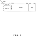
- An OTU frame has a structure of 4080 bytes ⁇ 4 rows as illustrated in FIG. 2 .
- the 1st to 16th bytes store control information.
- the control information includes an OTU overhead, an ODU (Optical channel Data Unit) overhead, and an OPU (Optical channel Payload Unit) overhead.
- the 17th to the 3824th bytes are a payload section and store client signals.
- An FEC Forward Error Correction
- An OTU frame is generated from an ODU (Optical channel Data Unit) frame. Although the OTU frame includes an FEC (Forward Error Correction), the PDU frame does not includes an FEC.
- ODU Optical channel Data Unit
- FEC Forward Error Correction
- OTN provides plural ODU/OTU each having different bit rates.
- OTN provides, for example, ODUO (1.244Gbps), ODU1 (2.498Gbps), ODU2 (10.037Gbps), ODU3 (40.319Gbps), ODU3 (104.794Gbps), and ODUflex (any bit rate) .
- ODU with a certain bit rate can be mapped into (or multiplexed into) another ODU with a different bit rate.
- ODU1 frames can be multiplexed into one ODU2 frame.
- LO_ODU low-speed ODU
- HO_ODU high-speed ODU
- tributary slots In the mapping of LO_ODU into HO_ODU, tributary slots (TS) are used. In other words, LO_ODU signals are temporarily allocated in the tributary slots. The signals allocated in the tributary slots are mapped into HO_ODU.
- the bit rate (or an allocation rate) of the tributary slots is fixed and is 1.25Gbps in a background example. Therefore, the number of tributary slots used in the mapping of LO_ODU into HO_ODU is determined in accordance with the bit rate of HO_ODU. For example, when HO_ODU is ODU2 and its bit rate is 10Gbps, the number of tributary slots used in the mapping is 8. When HO_ODU is ODU3 and its bit rate is 40Gbps, the number of tributary slots used in the mapping is 32.
- the number of tributary slots used in the mapping is 320.
- the signals allocated in the tributary slots are sequentially mapped byte by byte into the payload of HO_ODU, as illustrated in FIG. 3 .
- the signals in the tributary slots #1 to #320 are sequentially allocated in the payload of ODU frames.
- the signals of the first 1 byte of the tributary slots #1 to #320 are allocated to the 17th to the 336th bytes in the first row of the ODU frame 1, respectively.
- the signals of the next 1 byte of the tributary slots #1 to #320 are allocated to the 337th to the 656th bytes in the first row of the ODU frame 1, respectively.
- the number of tributary slots used in the mapping is 800.
- the signals allocated in the tributary slots are sequentially mapped byte by byte into the payload of HO_ODU, as illustrated in FIG. 4 .
- the frame generator circuit that generates OTU frames by performing the mapping of LO_ODU into HO_ODU may include a circuit that processes the signals of plural tributary slots in parallel.
- the frame generator circuit includes a circuit that establishes frame synchronization by using the signals allocated in the tributary slots.
- the transmission apparatus of the embodiment described below has a function or a configuration that solve this problem.
- FIG. 5 illustrates a configuration of a transmission apparatus at transmitter end.
- a transmission apparatus 10 has a client signal processor 11, a frame processor 12, and an optical transmission module 13.
- the transmission apparatus 10 is connected with a client device. It should be noted that the transmission apparatus 10 may correspond to the transmission apparatus 1A in the example illustrated in FIG. 1 .
- the client signal processor 11 terminates a client signal transmitted from the client device. It should be noted that the transmission apparatus 10 can accommodate plural client devices. In other words, the client signal processor 11 can terminate plural client signals.
- the frame processor 12 generates OTU frames to store the client signals terminated by the client signal processor 11. At that time, the frame processor 12 generates the LO_ODU frames at first to store the client signals. Next, the frame processor 12 maps the LO_ODU frames into HO_ODU frames. In this mapping, the signals in the LO_ODU frames are temporality allocated to the tributary slots. In other words, the tributary slots are used as intermediate frames between the LO_ODU frames and the HO_ODU frames. It should be noted that the frame processor 12 can perform the mapping of plural LO_ODU frames into a single HO_ODU frame. In this case, the plural LO_ODU frames are multiplexed into an HO_ODU frame. The frame processor 12 generates an OTU frame from the HO_ODU frames.
- the optical transmission module 13 generates an optical signal to transmit the OTU frame generated by the frame processor 12.
- the optical signal generated by the optical transmission module 13 is transmitted to the transmission apparatus at receiver end through the optical transmission path 3.
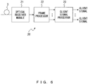
- FIG. 6 illustrates a configuration of the transmission apparatus at receiver end.
- the transmission apparatus 20 has an optical receiver module 21, a frame processor 22, and a client signal processor 23.
- the transmission apparatus 20 is connected with a client device. It should be noted that the transmission apparatus 20 may correspond to the transmission apparatus 1B in the example illustrated in FIG. 1 .
- the optical receiver module 21 receives the optical signal transmitted from the transmission apparatus at transmitter end (i.e., the transmission apparatus 10 in FIG. 5 ).
- the optical receiver module 21 converts the optical signal into electrical signal.
- the frame processor 22 reproduces the OTU frame from the output signal of the optical receiver modules 21. Then the frame processor 22 reproduces the client signals by processing the OTU frame. It should be noted that the processing in which the frame processor 22 reproduces the client signals from the OTU frame is substantially the inverse processing of the processing in which the frame processor 12 generates the OTU frame from the client signals.
- the client signal processor 23 transmits the client signals reproduced by the frame processor 22 to corresponding client devices. It should be noted that when plural client signals are reproduced by the frame processor 22, the client signal processor 23 transmits the client signals to the respective client devices.
- the transmission apparatus 10 illustrated in FIG. 5 may include the optical receiver module 21, the frame processor 22, and the client signal processor 23 illustrated in FIG. 6 so as to receive optical signals from other transmission apparatuses.
- the transmission apparatus 20 illustrated in FIG. 6 may include the client signal processor 11, the frame processor 12, and the optical transmission module 13 illustrated in FIG. 5 so as to transmit optical signals to other transmission apparatuses.
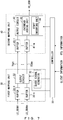
- FIG. 7 is a diagram explaining a mapping function of the frame processor 12 provided in the transmission apparatus at transmitter end.
- the frame processor 12 performs mapping of LO_ODU frames into HO_ODU frames as described above.
- the frame processor 12 has the first mapping unit 30, the second mapping unit 40, and a controller 50.
- ODU frames are input to the first mapping unit 30 through plural LO_ODUs #1 to #n.
- Each LO_ODU transmits an ODU frame that stores a client signal.
- the frame processor 12 has a function of generating an ODU frame that stores an input client signal, which is not illustrated in the drawing.
- each LO_ODU transmits an ODU frame that stores a client signal transmitted from its corresponding client device.
- the LO_ODU frame may transmit an ODU frame that stores a multiplexed signal including plural client signals.
- LO_ODUs #1 to #n are not particularly limited but are realized by ODU0, ODU1, ODU2, ODU3, ODU 4, or ODUflex.
- ODU2 may include ODU2e.
- ODU3 may include ODU3e.
- the bit rates of LO_ODUs #1 to #n are the same within one embodiment. However, the bit rates of LO_ODUs #1 to #n may not be always the same.
- the first mapping unit 30 includes buffers 31-1 to 31-n, a clock signal generator 32, and an output circuit 33.
- the first mapping unit 30 has output ports #1 to #m, although they are not specifically illustrated. It should be noted that the first mapping unit 30 may include other circuit elements.
- the buffers 31-1 to 31-n respectively store an ODU frame from received via LO_ODUs #1 to #n.
- the ODU frame is divided into 4 ⁇ 3824 frame elements, for example.
- each of the frame elements has 1 byte.
- These frame elements are sequentially written into the corresponding buffers (31-1 to 31-n) respectively.
- the signals in the 1st byte to the 3824th byte in the first row in the ODU frame are sequentially written into the corresponding buffers.
- the signals in the 1st byte to the 3824th byte in the second row, the signals in the 1st byte to the 3824th byte in the third row, and the signals in the 1st byte to the 3824th byte in the fourth row are sequentially written in this order in the corresponding buffers.
- the clock signal generator 32 generates a clock signal that has a frequency indicated by the controller 50. This frequency corresponds to the bit rate of tributary slots, which is described later.
- the clock signal generated by the clock signal generator 32 is supplied to the output circuit 33.
- the output circuit 33 retrieves signals stored in the buffers 31-1 to 31-n by using the clock signal generated by the clock signal generator 32. At that time, for example, the output circuit 33 retrieves the signals byte by byte from the buffers 31-1 to 31-n. The output circuit 33 guides the signals retrieved from the buffers 31-1 to 31-n to the corresponding output ports #1 to #m in accordance with the instructions provided by the controller 50.
- the output circuit 33 guides the signals retrieved from the buffers 31-1 to 31-n to the corresponding output ports #1 to #m.
- the output ports #1 to #m correspond to tributary slots TS #1 to #m, respectively.
- the signals output through the output ports #1 to #m are respectively allocated to the tributary slots TS #1 to #m.
- the output signals of the output ports #1 to #m are written in buffers 41-1 to 41-m of the second mapping unit 40, which is described later. Therefore, in this embodiment, "allocating to tributary slots" may be realized as a result of the processing of writing the output signals of the output ports #1 to # in the buffers 41-1 to 41-m, for example.
- the processing of retrieving signals from the buffers at a rate designated as a bit rate of tributary slots is also an example of "allocating to tributary slots". In other words, "allocating to tributary slots" is not limited to the processing of storing signals in memories etc.
- the first mapping unit 30 allocates the signals of LO_ODUs #1 to #n to the tributary slots TS #1 to #m.
- the bit rate of the tributary slots TS #1 to #m is designated by the controller 50 as explained later.
- the second mapping unit 40 includes buffers 41-1 to 41-m and an output circuit 42.
- the buffers 41-1 to 41-m store the signals of the tributary slots TS #1 to #m, respectively.
- the output circuit 42 retrieves the signals stored in the buffers 41-1 to 41-m by using the clock signal with a specified frequency. This frequency corresponds to the bit rate of the OTN frame transmitted by the transmitter apparatus 10. At that time, the output circuit 42 sequentially retrieves the signals from the buffer 41-1 to 41-m byte by byte, for example.
- the output circuit 42 includes an overhead adding unit 43 and a stuff inserting unit 44.
- the overhead adding unit 43 generates an overhead of an ODU frame. It should be noted that the ODU frame payload stores signals retrieved from the buffers 41-1 to 41-m.
- the stuff inserting unit 44 adds stuff bits at the end of the payload of an ODU frame, if necessary.
- the output circuit 42 outputs the generated an ODU frame as a HO_ODU frame.
- the transmission apparatus 10 generates an OTU frame from the HO_ODU frame output from the second mapping unit 40.
- the OTU frame has FEC as illustrated in FIG. 2 .
- the controller 50 controls the first mapping unit 30 and the second mapping unit 40 based on the OTU information and the client information.
- the OTU information includes information indicating the bit rate of the OTU frame transmitted by the transmission apparatus 10.
- the client information includes information indicating the bit rate of each of the input client signals as illustrated in FIG. 5 . It should be noted that the transmission apparatus 10 receives the OTU information and the client information from a network administrator or a network user, for example.
- the controller 50 recognizes the bit rate of HO_ODU based on the OTU information.
- an OTU frame has 4 ⁇ 4080 bytes as illustrated in FIG. 5 .
- an ODU frame has 4 ⁇ 3824 bytes since it does not have FEC.
- the bit rate of OTU corresponds to the bit rate of HO_ODU, but is not the same as the bit rate of HO_ODU.
- the bit rate of HO_ODU and the corresponding bit rate of OTU are the same for the sake of simplicity. For example, when the bit rate of OTU is 400Gbps, the corresponding bit rate of HO_ODU is 400Gbps.
- the controller 50 also recognizes a bit rate of each of LO_ODUs #1 to #n based on the client information. For example, when the client signals is 10GbE, the controller 50 determines that the corresponding LO_ODU is "ODU2e".
- the controller 50 determines the bit rate (or the allocation rate) of the tributary slots TS #1 to #m based on the bit rates of LO_ODUs #1 to #n and the bit rate of HO_ODU.
- the bit rates of the tributary slots TS #1 to #m are the same for the sake of simplicity.
- bit rates (1.25Gbps, 10Gbps, 40Gbps, 100Gbps, 400Gbps etc.) described in this specification are not the exact values, but are the approximate values.
- 10Gbps indicates approximately 10Gbps
- 40Gbps indicates approximately 40Gbps.
- the bit rates of the tributary slots TS #1 to #m are determined to be higher than or equal to the bit rates of LO_ODUs #1 to #n.
- the tributary slots TS #1 to #m are realized by "10Gbps ⁇ 40".
- the tributary slots TS #1 to #m may be realized by "40Gbps ⁇ 10" or "100Gbps ⁇ 4".
- a preferable configuration is such that a multiplexed signal of plural client signals (or plural LO_ODUs) is allocated in a single tributary slot TS.
- the controller 50 controls the first mapping unit 30 and the second mapping unit 40 based on the bit rate of tributary slots TS #1 to #m determined in the above manner.
- the clock signal generator 32 generates a clock signal with a frequency that corresponds to the bit rate of the tributary slots TS #1 to #m.
- the output circuit 33 retrieves and outputs the signals from the buffers 31-1 to 31-n by using this clock signal. As a result, the signals of the LO_ODUs #1 to #n are allocated to the tributary slots TS #1 to #m.
- the second mapping unit 40 generates an HO_ODU frame from the signals allocated to the tributary slots TS #1 to #m.
- FIG. 8 illustrates an example of mapping of LO_ODU into HO_ODU.
- the client signals #1 to #40 are input to the transmission apparatus 10.
- Each of the client signals #1 to #40 is 10GbE.
- ODU2e frames #1 to #40 are input in parallel as LO_ODUs #1 to #40 to the first mapping unit 30 illustrated in FIG. 7 .
- the bit rate of HO_ODU is 400Gbps.
- the LO_ODU frames #1 to #40 are sequentially stored in the corresponding buffers 31-1 to 31-n.
- the signals in the LO_ODU frames #1 are sequentially stored in the buffer 31-1.
- the output circuit 33 retrieves signals of the first byte (i.e., the first frame element) from each of the buffers 31-1 to 31-n by using the clock signal generated by the clock signal generator 32.
- frame elements A, C, and E are retrieved from LO_ODUs #1, #2, and #40, respectively.
- the frequency of the clock signal corresponds to the bit rate of the tributary slots TS #1 to #40 as described above.
- the output circuit 33 allocates the frame elements retrieved from the buffers 31-1 to 31-n to the corresponding tributary slots TS #1 to #40, respectively.
- the frame elements A, C, and E are allocated to the head of each of the tributary slots #1, #2, and #40, respectively.
- the output circuit 33 retrieves signals of the next byte (i.e., the second frame element) from each of the buffers 31-1 to 31-n in the next clock cycle. Then, the output circuit 33 allocates the frame elements retrieved from the buffers 31-1 to 31-n to the corresponding tributary slots TS#1 to #40, respectively.
- the frame elements B, D, and F are retrieved from the LO_ODU frames #1, #2, and #40, respectively.
- the frame elements B, D, and F are allocated to the second section of the tributary slots TS #1, #2, and #40, respectively.
- the output circuit 33 retrieves frame elements from each of the buffers 31-1 to 31-n in each clock cycle.
- the output circuit 33 allocates the frame elements retrieved from the buffers 31-1 to 31-n to the corresponding tributary slots TS #1 to #40.
- the tributary slots TS are 32 ⁇ 478 bytes in this example, although it is not limited to this capacity.
- the second mapping unit 40 allocates the signals (frame elements) allocated to the tributary slots TS #1 to #40 to the payload of the HO_ODU frame. In other words, the second mapping unit 40 allocates the frame elements allocated to the tributary slots #1 to #40 sequentially to the 16th to the 3824th bytes of the HO_ODU frame. At that time, in the example illustrated in FIG. 7 , the signals in the tributary slots TS #1 to #40 are temporarily stored in the buffers 41-1 to 41-m and afterwards, the signals are sequentially retrieved by the output circuit 42.
- the frame elements respectively allocated to the head of the respective tributary slots TS #1 to #40 are sequentially allocated to the 17th to the 56th bytes in the first row of the HO_ODU frame.
- the frame elements A, C, and E, each allocated to the head of the respective tributary slots TS #1, #2, and #40 are allocated to the 17th, the 18th, and the 56th bytes in the first row of the HO_ODU frame.
- the second frame elements that are respectively allocated in the tributary slots TS #1 to #40 are sequentially allocated to the 57th to the 96th bytes in the first row of the HO_ODU frame.
- the frame elements B, D, and F each allocated as the second frame elements of the tributary slots TS #1, #2, and #40, respectively, are allocated to the 57th, the 58th, and the 96th bytes in the first row of the HO_ODU frame.
- the stuff inserting unit 44 may insert the stuff at the end of the payload section of the HO_ODU frame, if necessary.
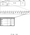
- FIG. 9 illustrates another example of mapping of LO_ODU into HO_ODU.
- the client signals #1 to #40 are input to the transmission apparatus 10.
- each of the client signals #1 to #40 is 10GbE.
- ODU2e frames #1 to #40 are input in parallel as LO_ODUs #1 to #40 to the first mapping unit 30 in FIG. 7 .
- the bit rate of HO_ODU is 400Gbps similarly to the example in FIG. 8 .
- the tributary slots TS #1 to #m are realized by "40Gbps ⁇ 10", which is different from the example in FIG. 8 .
- m 10
- the bit rate of each of the tributary slots TS #1 to #10 is 40Gbps.
- the output circuit 33 retrieves signals of the first byte (i.e., the first frame element) from each of the buffers 31-1 to 31-n by using the clock signal generated by the clock signal generator 32.
- frame elements A, B, and C are retrieved from the LO_ODU frames #1, #4, and #40, respectively.
- the frequency of the clock signal corresponds to the bit rate of the tributary slots TS #1 to #10 (i.e., 40Gbps).
- the output circuit 33 allocates the frame elements retrieved from the buffers 31-1 to 31-n to the corresponding tributary slots TS #1 to #10, respectively.
- the output circuit 33 multiplexes 4 LO_ODUs and allocates them to the corresponding tributary slot TS. For example, the output circuit 33 multiplexes LO_ODUs #1 to #4 and allocates them to the tributary slot TS #1. More specifically, the frame element A placed at the head of LO_ODU #1 is allocated to the head of the tributary slot TS #1, and the frame element B placed at the head of LO_ODU #4 is allocated to the fourth section of the tributary slot TS #1. In addition, the frame element C placed at the head of LO_ODU #40 is allocated to the fourth section of the tributary slot #10. It should be note that the frame element placed at the head of LO_ODU #37 is allocated to the head of the tributary slot TS #10, although it is not illustrated in the figure.
- the output circuit 33 retrieves the subsequent frame elements from the buffers 31-1 to 31-n at every clock cycles in the similar manner. Afterwards, the output circuit 33 multiplexes the frame elements retrieved from the buffers 31-1 to 31-n and allocates them to the corresponding tributary slots TS #1 to #10.
- the second mapping unit 40 allocates the signals allocated to the tributary slots TS #1 to #10 to the payload of the HO_ODU frame.
- the frame elements each allocated to the head of the respective tributary slots TS #1 to #10 are sequentially allocated to the 17th to the 26th bytes of the first row of the HO_ODU frame.
- the frame element A allocated to the head of the tributary slot TS #1 is allocated to the 17th byte of the first row of the HO_ODU frame.
- the subsequent data elements of the tributary slots TS #1 to #10 are allocated to the remaining payload section of the HO_ODU frame in the similar manner.
- the frame elements allocated as the fourth frame element of the tributary slots TS #1 to #10 are sequentially allocated to the 47th to the 56th bytes of the first row of the HO_ODU frame.
- the frame element B allocated as the fourth frame element of the tributary slot TS #1 is allocated to the 47th byte of the first row of the HO_ODU frame.
- the frame element C allocated as the fourth frame element of the tributary slot TS #10 is allocated to the 56th byte of the first row of the HO_ODU frame.
- FIG. 10 illustrates the other example of mapping of LO_ODU into HO_ODU.
- the client signals #1 to #40 are input to the transmission apparatus 10.
- each of the client signals #1 to #40 is 10GbE.
- ODU2e frames #1 to #40 are input in parallel as LO_ODUs #1 to #40 to the first mapping unit 30 in FIG. 7 .
- the bit rate of HO_ODU is 400Gbps similarly to the examples in FIG. 8 and FIG. 9 .
- the tributary slots TS #1 to #m are realized by "1.25Gbps ⁇ 320", which is different from the examples in FIG. 8 and FIG. 9 .
- m 320
- the bit rate of each of the tributary slots TS #1 to #320 is 1.25Gbps.
- the speed of the tributary slots TS is lower than LO_ODU. Therefore the signals of LO_ODU are distributed to plural tributary slots TS. For example, the signals of LO_ODU #1 are distributed to the tributary slots TS #1 to #8, and the signals of LO_ODU #40 are distributed to the tributary slots TS #313 to #320.
- the output circuit 33 retrieves 8 frame elements from each of LO_ODUs #1 to #40 and allocate them to 8 corresponding tributary slots TS. For example, the output circuit 33 retrieves 8 frame elements from LO_ODU #1 and allocate them to the tributary slots TS #1 to #8. In FIG. 10 , the frame elements A and B of LO_ODU #1 are allocated to the head of the tributary slots TS #1 and #2, respectively. The output circuit 33 also retrieves 8 frame elements from LO_ODU #40 and allocates them to the tributary slots TS #313 to #320. In FIG. 10 , the frame element C of LO_ODU #40 is allocated to the head of the tributary slot TS #320.
- the second mapping unit 40 allocates the signals allocated to the tributary slots TS #1 to #320 to the payload of the HO_ODU frame.
- the frame elements each allocated to the head of the respective tributary slots TS #1 to #320 are sequentially allocated to the 17th to the 336th bytes of the first row of the HO_ODU frame.
- the frame elements A, B, and C each allocated at the head of the respective tributary slots TS #1, #2, and #320 are allocated to the 17th, the 18th, and the 336th bytes of the first row of the HO_ODU frame, respectively.
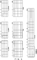
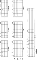
- FIG. 11 is a diagram explaining the calculation of the bit rate of tributary slots TS and bandwidth loss.
- the bit rate of the OTN frame transmitted from the transmission apparatus 10 is 449.219Gbps.
- the signals of the tributary slots TS are allocated to the payload of the HO_ODU frame as descried above. In other words, the signals of the tributary slots TS are allocated in the 17th to the 3824th bytes of an OTU frame.
- the transmission apparatus 10 provides 40 tributary slots TS #1 to #40, as illustrated in FIG. 11(a) , every 40 bytes of the payload section in each row of an ODU frame are assigned to the tributary slots TS #1 to #40. Consequently, the 17th to the 3816th bytes in each row are repeatedly assigned to the tributary slots #1 to #40. Therefore, an 8-byte stuff is inserted into the end of each row of the ODU frame.
- the bandwidth of each of the tributary slots #1 to #40 is 10.4597Gbps.
- the bandwidth loss i.e., the ratio of the stuff with respect to the bandwidth of the entire payload
- the bandwidth loss is about 0.21 percent.
- each of the tributary slots #1 to #10 is 41.839Gbps.
- the bandwidth loss is about 0.21 percent.
- each of the tributary slots #1 to #4 is 104.817Gbps. In addition, no bandwidth loss occurs.
- FIG. 12 is a diagram illustrating a background example of the mapping function of the frame processor 12 that may be provided in the transmission apparatus at transmitting end.
- the frame processor 12 includes a synchronization detector circuit 51, an ODTU buffer 52, a buffer controller 53, a GMP mapping unit 54, and an OTU frame generator 55.
- the synchronization detector circuit 51 detects frame synchronization in the tributary slots TS.
- the ODTU buffer 52 sequentially stores each of the plural ODTU frames generated from the plural LO_ODU frames.
- the buffer controller 53 controls the timing of retrieving the ODTU frame from the ODTU buffer 52 based on the synchronizing timing detected by the synchronization detector circuit 51.
- the GMP mapping unit 54 controls the mapping from ODTU to HO_ODU.
- the OTU frame generator 55 generates an OTU frame from HO_ODU.
- FIG. 13 to FIG. 15 are diagrams explaining the operations of the synchronization detector circuit 51.
- the client signals 1 to 4 are input to the transmission apparatus 10.
- Each of the client signals 1 to 4 is stored in the payload of an LO_ODU frame.
- 8 tributary slots TS #0 to #7 are used in the mapping from ODTU to HO_ODU.
- the correspondence between the client signals 1 to 4 and the tributary slots TS #0 to #7 are as below.
- Client signal 1 allocated to the tributary slots #0, #2, #3
- Client signal 2 allocated to the tributary slot #1
- Client signal 3 allocated to the tributary slots #4, #6
- Client signal 4 allocated to the tributary slots #5, #7
- the bit rate of the client signal 1 is three time faster than that of the tributary slots TS, and three tributary slots are assigned to the client signal 1.
- the bit rate of the client signal 2 is the same as that of the tributary slots TS, and one tributary slot is assigned to the client signal 2.
- the bit rates of the client signals 3 and 4 are twice faster than that of the tributary slots TS, and two tributary slots are assigned to each of the client signals 3 and 4.
- FAS Fram Alignment signal
- ODU frame 6-byte FAS (Frame Alignment signal)
- FAS is provided in the OTU overhead.
- FAS has a fixed pattern "F6 F6 F6 28 28 28" in this embodiment.
- LO_ODU that stores the client signal 1 is allocated to the tributary slots #0, #2, and #3
- LO_ODU that stores the client signal 2 is allocated to the tributary slot #1
- LO_ODU that stores the client signal 3 is allocated to the tributary slots #4 and #6
- LO_ODU that stores the client signal 4 is allocated to the tributary slots #5 and #7 at regular intervals.
- MFAS indicates Multi Frame Alignment Signal.
- Pay indicates payload data.
- the synchronization detector circuit 51 has a shift register illustrated in FIG. 14 .
- This shift register has 6 flip-flop circuits q0 to q5 to detect 6-byte synchronization information (i.e. , FAS).
- Each of the flip-flop circuits q0 to q5 stores 8-byte information.
- FIG. 14 illustrates a state in which the signals at the time T1, T2, T3, T4, T5, and T6 are stored in the flip-flop circuits q5, q4, q3, q2, q1, and q0, respectively.
- the synchronization detector circuit 51 sorts the signals stored in the flip-flop circuits q0 to q5 for the tributary slots TS. For example, the client signal 1 is allocated to the tributary slot TS #0. Here, the client signal 1 is also allocated to the tributary slots #2 and #3. Therefore when the tributary slot TS #0 signals stored in the flip-flop circuit q5 (i.e., the tributary slot TS #0 signals at the time T1) is the starting point, the client signal 1 is transmitted in the following order.
- the TS #0 signal [0] stored in the flip-flop circuit q5 The TS #2 signal [2] stored in the flip-flop circuit q5
- the client signal 1 will be transmitted in the following order.
- the TS #2 signal [2] stored in the flip-flop circuit q5 The TS #3 signal [3] stored in the flip-flop circuit q5
- the TS #0 signal [8] stored in the flip-flop circuit q4 The TS #2 signal [10] stored in the flip-flop circuit q4
- the TS #3 signal [11] stored in the flip-flop circuit q4 The TS #0 signal [16] stored in the flip-flop circuit q3
- the synchronization detector circuit 51 has the above sorting information for each of the tributary slots TS #0 to #8.
- the synchronization detector circuit 51 sorts the signals stored in the flip-flop circuits q0 to q5 based on this sorting information as described in FIG. 15 . For example, when the sorting is carried out on the tributary slot TS #0, the signals identified by [0], [2], [3], [8], [10], and [11] are arranged in order, and "pay F6 F6 F6 28 28" is consequently obtained.
- the sorting result for each tributary slot is provided in FIG. 15 .
- the synchronization detector circuit 51 compares the sorting result obtained with respect to the tributary slot TS #0 with the predetermined FAS pattern "F6 F6 F6 28 28 28". In this embodiment, synchronization is detected in the tributary slots TS #1, #2, and #5 as a result of this comparison.
- the synchronization detector circuit 51 detects synchronization while sequentially storing the signals in each of the tributary slots TS. Then, the frame processor 12 processes the frames based on the synchronization timing detected by the synchronization detector circuit 51.
- the synchronization detector circuit 51 has a shift register (the flip-flop circuits q0 to q5) as illustrated in FIG. 14 .
- Each of the flip-flop circuits q0 to q5 stores an amount of signals that depends on the number of the tributary slots TS. For example, since the frame processor 12 uses 8 tributary slots TS #0 to #7 illustrated in FIG. 13 to FIG. 15 , each flip-flop circuit stores an 8-byte signal. In this manner, since 40 tributary slots TS #1 to #40 are used in the embodiment illustrated in FIG. 8 , each flip-flop circuit stores a 40-byte signal. In the background example illustrated in FIG. 10 , which uses 320 tributary slots TS, each flip-flop circuit stores a 320-byte signal.
- the synchronization detector circuit 51 processes the signals of all the tributary slots TS in parallel.
- the transmission apparatus of the embodiment of the present invention reduces the number of tributary slots by increasing the bit rate of the tributary slots used in mapping of LO_ODU into HO_ODU.
- a circuit to transmit OTU frames which is faster than OTU4
- the size of the circuit for frame processing becomes smaller, and power consumption is suppressed.
- the circuit sizes of the ODTU buffer 52, the buffer controller 53, and the GMP mapping unit 54, which are illustrated in FIG. 12 become approximately 1/8.
- the bit rate of tributary slots is preferably set at a rate of ODU2/ODU2e or faster.
- the controller 50 controls the bit rate of tributary slots to be a bit rate obtained by dividing the bit rate of HO_ODU frame by a certain integer.
- the controller 50 controls the bit rate of tributary slots to be "10Gbps" that is obtained by dividing the bit rate of HO_ODU, i.e., 400Gbps, by "40".
- the first mapping unit 30 allocates the signals of LO_ODU frames to H/M tributary slots.
- the frame processing in the transmission apparatus 20 at receiver end is substantially equivalent to the inverse processing of the frame processing in the transmission apparatus 10 at transmitter end. Therefore, the transmission apparatus 20 at receiver end has a function of inverse mapping of the mapping in FIG. 7 .
- the transmission apparatus 20 at receiver end recognizes the change.
- the transmission apparatus 10 may notify the transmission apparatus 20 of the allocation rate of tributary slots by using the OTU overhead of an OTU frame.
- the allocation rate of tributary slots is indicated by using a reserved area in the 14th byte in the OTU overhead illustrated in FIG. 16 .
- normal, ODU2 allocation, ODU2e allocation, ODU3 allocation, and ODU4 allocation are identified by using 3-bit information.
- Normal indicates that the allocation rate of tributary slots is 1. 25Gbps or 2.5Gbps.
- ODU2 allocation indicates that the allocation rate of tributary slots is equivalent to ODU2.
- ODU2e allocation indicates that the allocation rate of tributary slots is equivalent to ODU2e.
- ODU3 allocation indicates that the allocation rate of tributary slots is equivalent to ODU3.
- ODU4 allocation indicates that the allocation rate of tributary slots is equivalent to ODU4.
- the transmission apparatus 20 at receiver end may recognize the allocation rate of tributary slots in the transmission apparatus 10 at transmitter end by using other schemes.
- a network management system may transmit information indicating the allocation rate of tributary slots to the transmission apparatuses 10 and 20.
Landscapes
- Engineering & Computer Science (AREA)
- Computer Networks & Wireless Communication (AREA)
- Signal Processing (AREA)
- Time-Division Multiplex Systems (AREA)
Description
- The present invention is related to a transmission apparatus that transmits signals in an optical network.
- OTN (Optical Transport Network), which is recommended by the ITU (International Telecommunication Union), have been known as one of the standards for transmitting signals in an optical network (e.g., core network). In OTN, client data is stored in OTU (Optical channel Transport Unit) frames and is transmitted.
- In recent years, further increases in speed have been needed in optical networks. In response to the need, for example, a frame generation apparatus that generates ODTU frames, a digital transmission system that provides flexible payload capacity in OTU, and a method of mapping any signals to SONET (Synchronous Optical Network) have been proposed.
-
- Patent Document 1: Japanese Laid-Open Patent Application Publication No.
2010-212890 - Patent Document 2: Japanese Laid-Open Patent Application Publication No.
2012-4839 - Patent Document 3: Japanese Laid-Open Patent Application Publication No.
2001-69104 - The document titled "Framework for GMPLS and PCE Control of G.709 Optical Transport Networks; draft-ietf-ccamp-gmpls-g709-framework-02.txt" by Fatai Zhang et al., FRAMEWORK FOR GMPLS AND PCE CONTROL OF G.709 OPTICAL TRANSPORT NETWORKS; DRAFT-IETF-CCAMP-GMPLS-G709-FRAMEWORK-02.TXT, INTERNET ENGINEERING TASK FORCE, IETF; STANDARDWORKINGDRAFT, INTERNET SOCIETY (ISOC), no. 2, 12 July 2010, pages 1-26, on which the two-part form of
Claim 1 is based, provides a framework to allow the development of protocol extensions to support Generalized Multiprotocol Label Switching (GMPLS) and Path Computation Element (PCE) control of Optical Transport Networks (OTN) as specified in ITU-T Recommendation G.709 as consented in October 2009. - As described above, technologies to increase the speed of optical networks have been proposed. However, as the optical networks increases their speed, the size of a circuit that processes OTU frames increases and the power consumption may also be increased.
- It is an object of the present invention to reduce the size or the power consumption of a circuit that controls mapping of the first frames into the second frame in a transmission apparatus that transmits frames.
- The present invention provides a transmission apparatus as set out in
Claim 1. - According to embodiments described herein, it is possible to reduce the size or the power consumption of a circuit that controls mapping of the first frames into the second frame in a transmission apparatus that transmits frames.
-
-
FIG. 1 illustrates an example of an optical transmission system in which a transmission apparatus of the embodiment of the present invention is used; -
FIG. 2 is a diagram illustrating a structure of an OTU frame; -
FIG. 3 is a diagram illustrating a method of allocating signals of 320 tributary slots to ODU frames; -
FIG. 4 is a diagram illustrating a method of allocating signals of 800 tributary slots to ODU frames; -
FIG. 5 illustrates a configuration of a transmission apparatus at transmitter end; -
FIG. 6 illustrates a configuration of a transmission apparatus at receiver end; -
FIG. 7 is a diagram explaining a mapping function of a frame processor provided in the transmission apparatus at transmitter end; -
FIG. 8 illustrates an example of mapping of LO_ODUs into HO_ODU; -
FIG. 9 illustrates another example of mapping of LO_ODUs into HO_ODU; -
FIG. 10 illustrates the other example of mapping of LO_ODUs into HO_ODU; -
FIG. 11 is a diagram explaining the bit rate of tributary slots TS and bandwidth loss; -
FIG. 12 is a diagram illustrating another example of a mapping function of the frame processor provided in the transmission apparatus at transmitting end; -
FIG. 13 is a diagram (1) explaining operations of a synchronization detector circuit; -
FIG. 14 is a diagram (2) explaining operations of a synchronization detector circuit; -
FIG. 15 is a diagram (3) explaining operations of a synchronization detector circuit; -
FIG. 16 is a diagram illustrating an example of a method of notifying the receiver end of an allocation rate of tributary slots. -
FIG. 1 illustrates an example of an optical transmission system in which a transmission apparatus of the embodiment of the present invention is used.Transmission apparatuses 1A and 1B can respectively accommodate aclient device 2. Thetransmission apparatuses 1A and 1B are connected to each other by anoptical transmission path 3. - The transmission apparatus 1A generates a frame that stores a client signal transmitted from the
client device 2. The transmission apparatus 1A transmits this frame to thetransmission apparatus 1B through theoptical transmission path 3. Thetransmission apparatus 1B reproduces the client signal from the frame received from the transmission apparatus 1A. Afterward, thetransmission apparatus 1B transfers the reproduced client signal to thecorresponding client device 2. - In the following descriptions, the transmission apparatus 1A may be referred to as a transmission apparatus at transmitter end. The
transmission apparatus 1B may be referred to as a transmission apparatus at receiver end. However, thetransmission apparatus 1B may have a function of transmitting an optical signal to the transmission apparatus 1A. The transmission apparatus 1A may have a function of receiving the optical signal from thetransmission apparatus 1B. - OTU frame, which is recommended by the ITU, is transmitted between the
transmission apparatuses 1A and 1B. An OTU frame has a structure of 4080 bytes × 4 rows as illustrated inFIG. 2 . The 1st to 16th bytes store control information. The control information includes an OTU overhead, an ODU (Optical channel Data Unit) overhead, and an OPU (Optical channel Payload Unit) overhead. The 17th to the 3824th bytes are a payload section and store client signals. An FEC (Forward Error Correction) is added to the 3825th to the 4080th bytes. - An OTU frame is generated from an ODU (Optical channel Data Unit) frame. Although the OTU frame includes an FEC (Forward Error Correction), the PDU frame does not includes an FEC.
- The client signals are stored in the payload of the ODU frame. Here, OTN provides plural ODU/OTU each having different bit rates. In other words, OTN provides, for example, ODUO (1.244Gbps), ODU1 (2.498Gbps), ODU2 (10.037Gbps), ODU3 (40.319Gbps), ODU3 (104.794Gbps), and ODUflex (any bit rate) . It should be noted that, for the sake of simplicity, the bit rates provided in this specification are ODUO=1.25Gbps, ODU1=2.5Gbps, ODU2=10Gbps, ODU3=40Gbps, and ODU4=100Gbps.
- In OTN, ODU with a certain bit rate can be mapped into (or multiplexed into) another ODU with a different bit rate. For example, four ODU1 frames can be multiplexed into one ODU2 frame. In the following descriptions, a low-speed ODU may be referred to as "LO_ODU" and a high-speed ODU may be referred to as "HO_ODU".
- In the mapping of LO_ODU into HO_ODU, tributary slots (TS) are used. In other words, LO_ODU signals are temporarily allocated in the tributary slots. The signals allocated in the tributary slots are mapped into HO_ODU.
- The bit rate (or an allocation rate) of the tributary slots is fixed and is 1.25Gbps in a background example. Therefore, the number of tributary slots used in the mapping of LO_ODU into HO_ODU is determined in accordance with the bit rate of HO_ODU. For example, when HO_ODU is ODU2 and its bit rate is 10Gbps, the number of tributary slots used in the mapping is 8. When HO_ODU is ODU3 and its bit rate is 40Gbps, the number of tributary slots used in the mapping is 32.
- Under such conditions, further increase in the speed of optical networks has been requested. In OTN, transmission schemes that have a bandwidth of 400Gbps or 1Tbps have been explored as the next-generation standards of ODU4/OTU4. In such schemes, a transmission apparatus that transmits OTU frames will need to perform mapping of any of ODU0 to ODU4 into 400Gbps/1TGbps ODU.
- For example, when HO_ODU is 400Gbps, the number of tributary slots used in the mapping is 320. In this case, the signals allocated in the tributary slots are sequentially mapped byte by byte into the payload of HO_ODU, as illustrated in
FIG. 3 . - In the example illustrated in
FIG. 3 , the signals in thetributary slots # 1 to #320 are sequentially allocated in the payload of ODU frames. For example, the signals of the first 1 byte of thetributary slots # 1 to #320 are allocated to the 17th to the 336th bytes in the first row of theODU frame 1, respectively. The signals of the next 1 byte of thetributary slots # 1 to #320 are allocated to the 337th to the 656th bytes in the first row of theODU frame 1, respectively. - When HO_ODU is 1Tbps, the number of tributary slots used in the mapping is 800. In this case, the signals allocated in the tributary slots are sequentially mapped byte by byte into the payload of HO_ODU, as illustrated in
FIG. 4 . - As described above, the number of tributary slots increases when further increase in the speed of optical networks is achieved. However, the frame generator circuit that generates OTU frames by performing the mapping of LO_ODU into HO_ODU may include a circuit that processes the signals of plural tributary slots in parallel. For example, in the mapping of LO_ODU into HO_ODU, the frame generator circuit includes a circuit that establishes frame synchronization by using the signals allocated in the tributary slots.
- When the number of tributary slots increases along with the increase in the speed of optical networks, the circuit size and power consumption of the frame generator circuit may possibly be increased. Considering this, the transmission apparatus of the embodiment described below has a function or a configuration that solve this problem.
-
FIG. 5 illustrates a configuration of a transmission apparatus at transmitter end. Atransmission apparatus 10 has aclient signal processor 11, aframe processor 12, and anoptical transmission module 13. Thetransmission apparatus 10 is connected with a client device. It should be noted that thetransmission apparatus 10 may correspond to the transmission apparatus 1A in the example illustrated inFIG. 1 . - The
client signal processor 11 terminates a client signal transmitted from the client device. It should be noted that thetransmission apparatus 10 can accommodate plural client devices. In other words, theclient signal processor 11 can terminate plural client signals. - The
frame processor 12 generates OTU frames to store the client signals terminated by theclient signal processor 11. At that time, theframe processor 12 generates the LO_ODU frames at first to store the client signals. Next, theframe processor 12 maps the LO_ODU frames into HO_ODU frames. In this mapping, the signals in the LO_ODU frames are temporality allocated to the tributary slots. In other words, the tributary slots are used as intermediate frames between the LO_ODU frames and the HO_ODU frames. It should be noted that theframe processor 12 can perform the mapping of plural LO_ODU frames into a single HO_ODU frame. In this case, the plural LO_ODU frames are multiplexed into an HO_ODU frame. Theframe processor 12 generates an OTU frame from the HO_ODU frames. - The
optical transmission module 13 generates an optical signal to transmit the OTU frame generated by theframe processor 12. The optical signal generated by theoptical transmission module 13 is transmitted to the transmission apparatus at receiver end through theoptical transmission path 3. -
FIG. 6 illustrates a configuration of the transmission apparatus at receiver end. Thetransmission apparatus 20 has anoptical receiver module 21, aframe processor 22, and aclient signal processor 23. Thetransmission apparatus 20 is connected with a client device. It should be noted that thetransmission apparatus 20 may correspond to thetransmission apparatus 1B in the example illustrated inFIG. 1 . - The
optical receiver module 21 receives the optical signal transmitted from the transmission apparatus at transmitter end (i.e., thetransmission apparatus 10 inFIG. 5 ). Theoptical receiver module 21 converts the optical signal into electrical signal. - The
frame processor 22 reproduces the OTU frame from the output signal of theoptical receiver modules 21. Then theframe processor 22 reproduces the client signals by processing the OTU frame. It should be noted that the processing in which theframe processor 22 reproduces the client signals from the OTU frame is substantially the inverse processing of the processing in which theframe processor 12 generates the OTU frame from the client signals. - The
client signal processor 23 transmits the client signals reproduced by theframe processor 22 to corresponding client devices. It should be noted that when plural client signals are reproduced by theframe processor 22, theclient signal processor 23 transmits the client signals to the respective client devices. - It should be noted that the
transmission apparatus 10 illustrated inFIG. 5 may include theoptical receiver module 21, theframe processor 22, and theclient signal processor 23 illustrated inFIG. 6 so as to receive optical signals from other transmission apparatuses. Similarly, thetransmission apparatus 20 illustrated inFIG. 6 may include theclient signal processor 11, theframe processor 12, and theoptical transmission module 13 illustrated inFIG. 5 so as to transmit optical signals to other transmission apparatuses. -
FIG. 7 is a diagram explaining a mapping function of theframe processor 12 provided in the transmission apparatus at transmitter end. Theframe processor 12 performs mapping of LO_ODU frames into HO_ODU frames as described above. In order to realize this mapping, theframe processor 12 has thefirst mapping unit 30, thesecond mapping unit 40, and acontroller 50. - ODU frames are input to the
first mapping unit 30 throughplural LO_ODUs # 1 to #n. Each LO_ODU transmits an ODU frame that stores a client signal. Here, theframe processor 12 has a function of generating an ODU frame that stores an input client signal, which is not illustrated in the drawing. For example, each LO_ODU transmits an ODU frame that stores a client signal transmitted from its corresponding client device. Alternatively, the LO_ODU frame may transmit an ODU frame that stores a multiplexed signal including plural client signals. -
LO_ODUs # 1 to #n are not particularly limited but are realized by ODU0, ODU1, ODU2, ODU3,ODU 4, or ODUflex. ODU2 may include ODU2e. ODU3 may include ODU3e. The bit rates ofLO_ODUs # 1 to #n are the same within one embodiment. However, the bit rates ofLO_ODUs # 1 to #n may not be always the same. - The
first mapping unit 30 includes buffers 31-1 to 31-n, aclock signal generator 32, and anoutput circuit 33. Thefirst mapping unit 30 hasoutput ports # 1 to #m, although they are not specifically illustrated. It should be noted that thefirst mapping unit 30 may include other circuit elements. - The buffers 31-1 to 31-n respectively store an ODU frame from received via
LO_ODUs # 1 to #n. At that time, the ODU frame is divided into 4 × 3824 frame elements, for example. In this case, each of the frame elements has 1 byte. These frame elements are sequentially written into the corresponding buffers (31-1 to 31-n) respectively. As an example, initially, the signals in the 1st byte to the 3824th byte in the first row in the ODU frame are sequentially written into the corresponding buffers. Subsequently, the signals in the 1st byte to the 3824th byte in the second row, the signals in the 1st byte to the 3824th byte in the third row, and the signals in the 1st byte to the 3824th byte in the fourth row are sequentially written in this order in the corresponding buffers. - The
clock signal generator 32 generates a clock signal that has a frequency indicated by thecontroller 50. This frequency corresponds to the bit rate of tributary slots, which is described later. The clock signal generated by theclock signal generator 32 is supplied to theoutput circuit 33. - The
output circuit 33 retrieves signals stored in the buffers 31-1 to 31-n by using the clock signal generated by theclock signal generator 32. At that time, for example, theoutput circuit 33 retrieves the signals byte by byte from the buffers 31-1 to 31-n. Theoutput circuit 33 guides the signals retrieved from the buffers 31-1 to 31-n to the correspondingoutput ports # 1 to #m in accordance with the instructions provided by thecontroller 50. - In one embodiment, the number of
LO_ODUs # 1 to #n and the number of theoutput ports # 1 to #m are the same. In other words, n = m. In this case, theoutput circuit 33 guides the signals retrieved from the buffers 31-1 to 31-n to the correspondingoutput ports # 1 to #m. - The
output ports # 1 to #m correspond to tributaryslots TS # 1 to #m, respectively. In other words, the signals output through theoutput ports # 1 to #m are respectively allocated to the tributaryslots TS # 1 to #m. - Here, the output signals of the
output ports # 1 to #m are written in buffers 41-1 to 41-m of thesecond mapping unit 40, which is described later. Therefore, in this embodiment, "allocating to tributary slots" may be realized as a result of the processing of writing the output signals of theoutput ports # 1 to # in the buffers 41-1 to 41-m, for example. However, the processing of retrieving signals from the buffers at a rate designated as a bit rate of tributary slots is also an example of "allocating to tributary slots". In other words, "allocating to tributary slots" is not limited to the processing of storing signals in memories etc. - In this manner, the
first mapping unit 30 allocates the signals ofLO_ODUs # 1 to #n to the tributaryslots TS # 1 to #m. Here, the bit rate of the tributaryslots TS # 1 to #m is designated by thecontroller 50 as explained later. - The
second mapping unit 40 includes buffers 41-1 to 41-m and anoutput circuit 42. The buffers 41-1 to 41-m store the signals of the tributaryslots TS # 1 to #m, respectively. - The
output circuit 42 retrieves the signals stored in the buffers 41-1 to 41-m by using the clock signal with a specified frequency. This frequency corresponds to the bit rate of the OTN frame transmitted by thetransmitter apparatus 10. At that time, theoutput circuit 42 sequentially retrieves the signals from the buffer 41-1 to 41-m byte by byte, for example. - The
output circuit 42 includes anoverhead adding unit 43 and astuff inserting unit 44. Theoverhead adding unit 43 generates an overhead of an ODU frame. It should be noted that the ODU frame payload stores signals retrieved from the buffers 41-1 to 41-m. Thestuff inserting unit 44 adds stuff bits at the end of the payload of an ODU frame, if necessary. Theoutput circuit 42 outputs the generated an ODU frame as a HO_ODU frame. - It should be noted that the
transmission apparatus 10 generates an OTU frame from the HO_ODU frame output from thesecond mapping unit 40. The OTU frame has FEC as illustrated inFIG. 2 . - The
controller 50 controls thefirst mapping unit 30 and thesecond mapping unit 40 based on the OTU information and the client information. - The OTU information includes information indicating the bit rate of the OTU frame transmitted by the
transmission apparatus 10. The client information includes information indicating the bit rate of each of the input client signals as illustrated inFIG. 5 . It should be noted that thetransmission apparatus 10 receives the OTU information and the client information from a network administrator or a network user, for example. - The
controller 50 recognizes the bit rate of HO_ODU based on the OTU information. Here, an OTU frame has 4 × 4080 bytes as illustrated inFIG. 5 . On the other hand, an ODU frame has 4 × 3824 bytes since it does not have FEC. Accordingly, the bit rate of OTU corresponds to the bit rate of HO_ODU, but is not the same as the bit rate of HO_ODU. However, in the following descriptions, the bit rate of HO_ODU and the corresponding bit rate of OTU are the same for the sake of simplicity. For example, when the bit rate of OTU is 400Gbps, the corresponding bit rate of HO_ODU is 400Gbps. - The
controller 50 also recognizes a bit rate of each ofLO_ODUs # 1 to #n based on the client information. For example, when the client signals is 10GbE, thecontroller 50 determines that the corresponding LO_ODU is "ODU2e". - The
controller 50 determines the bit rate (or the allocation rate) of the tributaryslots TS # 1 to #m based on the bit rates ofLO_ODUs # 1 to #n and the bit rate of HO_ODU. In the following descriptions, the bit rates of the tributaryslots TS # 1 to #m are the same for the sake of simplicity. - When the bit rate of HO_ODU is H, and the bit rate of tributary
slots TS # 01 to #m is M, the bit rate and the number of tributary slots TS are determined so as to satisfy an equation H = m × M. More particularly, when the bit rate of HO_ODU is 400Gbps, the tributaryslots TS # 1 to #m are realized by "10Gbps × 40", "40Gbps × 10", or "100Gbps × 4". - It should be noted that as described above, the bit rates
(1.25Gbps, 10Gbps, 40Gbps, 100Gbps, 400Gbps etc.) described in this specification are not the exact values, but are the approximate values. For example, "10Gbps" indicates approximately 10Gbps, and "40Gbps" indicates approximately 40Gbps. In addition, the above provided equation "H = m × M" indicates an approximate relationship. - The bit rates of the tributary
slots TS # 1 to #m are determined to be higher than or equal to the bit rates ofLO_ODUs # 1 to #n. As an example, when each client signal is 10GbE, the tributaryslots TS # 1 to #m are realized by "10Gbps × 40". It should be noted that when each client signal is 10GbE, the tributaryslots TS # 1 to #m may be realized by "40Gbps × 10" or "100Gbps × 4". However, in this case, a preferable configuration is such that a multiplexed signal of plural client signals (or plural LO_ODUs) is allocated in a single tributary slot TS. - The
controller 50 controls thefirst mapping unit 30 and thesecond mapping unit 40 based on the bit rate of tributaryslots TS # 1 to #m determined in the above manner. In other words, theclock signal generator 32 generates a clock signal with a frequency that corresponds to the bit rate of the tributaryslots TS # 1 to #m. Theoutput circuit 33 retrieves and outputs the signals from the buffers 31-1 to 31-n by using this clock signal. As a result, the signals of theLO_ODUs # 1 to #n are allocated to the tributaryslots TS # 1 to #m. Thesecond mapping unit 40 generates an HO_ODU frame from the signals allocated to the tributaryslots TS # 1 to #m. -
FIG. 8 illustrates an example of mapping of LO_ODU into HO_ODU. In this example, the client signals #1 to #40 are input to thetransmission apparatus 10. Each of the client signals #1 to #40 is 10GbE. In other words, ODU2e frames #1 to #40 are input in parallel asLO_ODUs # 1 to #40 to thefirst mapping unit 30 illustrated inFIG. 7 . The bit rate of HO_ODU is 400Gbps. The tributaryslots TS # 1 to #m are realized by "10Gbps × 40". In other words, m=40 and the bit rate of each of the tributaryslots TS # 1 to #40 is 10Gbps. - The LO_ODU frames #1 to #40 are sequentially stored in the corresponding buffers 31-1 to 31-n. For example, the signals in the LO_ODU frames #1 are sequentially stored in the buffer 31-1.
- The
output circuit 33 retrieves signals of the first byte (i.e., the first frame element) from each of the buffers 31-1 to 31-n by using the clock signal generated by theclock signal generator 32. InFIG. 8 , frame elements A, C, and E are retrieved fromLO_ODUs # 1, #2, and #40, respectively. The frequency of the clock signal corresponds to the bit rate of the tributaryslots TS # 1 to #40 as described above. Theoutput circuit 33 allocates the frame elements retrieved from the buffers 31-1 to 31-n to the corresponding tributaryslots TS # 1 to #40, respectively. InFIG. 8 , the frame elements A, C, and E are allocated to the head of each of thetributary slots # 1, #2, and #40, respectively. - The
output circuit 33 retrieves signals of the next byte (i.e., the second frame element) from each of the buffers 31-1 to 31-n in the next clock cycle. Then, theoutput circuit 33 allocates the frame elements retrieved from the buffers 31-1 to 31-n to the corresponding tributaryslots TS# 1 to #40, respectively. InFIG. 8 , the frame elements B, D, and F are retrieved from the LO_ODU frames #1, #2, and #40, respectively. The frame elements B, D, and F are allocated to the second section of the tributaryslots TS # 1, #2, and #40, respectively. - In the following descriptions, similarly, the
output circuit 33 retrieves frame elements from each of the buffers 31-1 to 31-n in each clock cycle. Theoutput circuit 33 allocates the frame elements retrieved from the buffers 31-1 to 31-n to the corresponding tributaryslots TS # 1 to #40. It should be noted that the tributary slots TS are 32 × 478 bytes in this example, although it is not limited to this capacity. - The
second mapping unit 40 allocates the signals (frame elements) allocated to the tributaryslots TS # 1 to #40 to the payload of the HO_ODU frame. In other words, thesecond mapping unit 40 allocates the frame elements allocated to thetributary slots # 1 to #40 sequentially to the 16th to the 3824th bytes of the HO_ODU frame. At that time, in the example illustrated inFIG. 7 , the signals in the tributaryslots TS # 1 to #40 are temporarily stored in the buffers 41-1 to 41-m and afterwards, the signals are sequentially retrieved by theoutput circuit 42. - In the example illustrated in
FIG. 8 , the frame elements respectively allocated to the head of the respective tributaryslots TS # 1 to #40 are sequentially allocated to the 17th to the 56th bytes in the first row of the HO_ODU frame. For example, the frame elements A, C, and E, each allocated to the head of the respective tributaryslots TS # 1, #2, and #40, are allocated to the 17th, the 18th, and the 56th bytes in the first row of the HO_ODU frame. - Next, the second frame elements that are respectively allocated in the tributary
slots TS # 1 to #40 are sequentially allocated to the 57th to the 96th bytes in the first row of the HO_ODU frame. For example, the frame elements B, D, and F each allocated as the second frame elements of the tributaryslots TS # 1, #2, and #40, respectively, are allocated to the 57th, the 58th, and the 96th bytes in the first row of the HO_ODU frame. - Then the subsequent data elements of the tributary
slots TS # 1 to #40 are allocated to the remaining payload section of the HO_ODU frame in the similar manner. At that time thestuff inserting unit 44 may insert the stuff at the end of the payload section of the HO_ODU frame, if necessary. -
FIG. 9 illustrates another example of mapping of LO_ODU into HO_ODU. In this example, the client signals #1 to #40 are input to thetransmission apparatus 10. Similarly to the example inFIG. 8 , each of the client signals #1 to #40 is 10GbE. In other words, ODU2e frames #1 to #40 are input in parallel asLO_ODUs # 1 to #40 to thefirst mapping unit 30 inFIG. 7 . The bit rate of HO_ODU is 400Gbps similarly to the example inFIG. 8 . However, the tributaryslots TS # 1 to #m are realized by "40Gbps × 10", which is different from the example inFIG. 8 . In other words, m=10, and the bit rate of each of the tributaryslots TS # 1 to #10 is 40Gbps. - The
output circuit 33 retrieves signals of the first byte (i.e., the first frame element) from each of the buffers 31-1 to 31-n by using the clock signal generated by theclock signal generator 32. InFIG. 9 , frame elements A, B, and C are retrieved from the LO_ODU frames #1, #4, and #40, respectively. However, the frequency of the clock signal corresponds to the bit rate of the tributaryslots TS # 1 to #10 (i.e., 40Gbps). Theoutput circuit 33 allocates the frame elements retrieved from the buffers 31-1 to 31-n to the corresponding tributaryslots TS # 1 to #10, respectively. - At that time, the
output circuit 33multiplexes 4 LO_ODUs and allocates them to the corresponding tributary slot TS. For example, theoutput circuit 33multiplexes LO_ODUs # 1 to #4 and allocates them to the tributaryslot TS # 1. More specifically, the frame element A placed at the head ofLO_ODU # 1 is allocated to the head of the tributaryslot TS # 1, and the frame element B placed at the head ofLO_ODU # 4 is allocated to the fourth section of the tributaryslot TS # 1. In addition, the frame element C placed at the head ofLO_ODU # 40 is allocated to the fourth section of thetributary slot # 10. It should be note that the frame element placed at the head ofLO_ODU # 37 is allocated to the head of the tributaryslot TS # 10, although it is not illustrated in the figure. - Then the
output circuit 33 retrieves the subsequent frame elements from the buffers 31-1 to 31-n at every clock cycles in the similar manner. Afterwards, theoutput circuit 33 multiplexes the frame elements retrieved from the buffers 31-1 to 31-n and allocates them to the corresponding tributaryslots TS # 1 to #10. - The
second mapping unit 40 allocates the signals allocated to the tributaryslots TS # 1 to #10 to the payload of the HO_ODU frame. In the example illustrated inFIG. 9 , the frame elements each allocated to the head of the respective tributaryslots TS # 1 to #10 are sequentially allocated to the 17th to the 26th bytes of the first row of the HO_ODU frame. For example, the frame element A allocated to the head of the tributaryslot TS # 1 is allocated to the 17th byte of the first row of the HO_ODU frame. - Then the subsequent data elements of the tributary
slots TS # 1 to #10 are allocated to the remaining payload section of the HO_ODU frame in the similar manner. For example, the frame elements allocated as the fourth frame element of the tributaryslots TS # 1 to #10 are sequentially allocated to the 47th to the 56th bytes of the first row of the HO_ODU frame. At that time, the frame element B allocated as the fourth frame element of the tributaryslot TS # 1 is allocated to the 47th byte of the first row of the HO_ODU frame. In addition, the frame element C allocated as the fourth frame element of the tributaryslot TS # 10 is allocated to the 56th byte of the first row of the HO_ODU frame. -
FIG. 10 illustrates the other example of mapping of LO_ODU into HO_ODU. In this background example, the client signals #1 to #40 are input to thetransmission apparatus 10. Similarly to the examples inFIG. 8 andFIG. 9 , each of the client signals #1 to #40 is 10GbE. In other words, ODU2e frames #1 to #40 are input in parallel asLO_ODUs # 1 to #40 to thefirst mapping unit 30 inFIG. 7 . The bit rate of HO_ODU is 400Gbps similarly to the examples inFIG. 8 andFIG. 9 . However, the tributaryslots TS # 1 to #m are realized by "1.25Gbps × 320", which is different from the examples inFIG. 8 andFIG. 9 . In other words, m=320, and the bit rate of each of the tributaryslots TS # 1 to #320 is 1.25Gbps. - In this background example, the speed of the tributary slots TS is lower than LO_ODU. Therefore the signals of LO_ODU are distributed to plural tributary slots TS. For example, the signals of
LO_ODU # 1 are distributed to the tributaryslots TS # 1 to #8, and the signals ofLO_ODU # 40 are distributed to the tributary slots TS #313 to #320. - The
output circuit 33retrieves 8 frame elements from each ofLO_ODUs # 1 to #40 and allocate them to 8 corresponding tributary slots TS. For example, theoutput circuit 33retrieves 8 frame elements fromLO_ODU # 1 and allocate them to the tributaryslots TS # 1 to #8. InFIG. 10 , the frame elements A and B ofLO_ODU # 1 are allocated to the head of the tributaryslots TS # 1 and #2, respectively. Theoutput circuit 33 also retrieves 8 frame elements fromLO_ODU # 40 and allocates them to the tributary slots TS #313 to #320. InFIG. 10 , the frame element C ofLO_ODU # 40 is allocated to the head of the tributaryslot TS # 320. - The
second mapping unit 40 allocates the signals allocated to the tributaryslots TS # 1 to #320 to the payload of the HO_ODU frame. In the example illustrated inFIG. 10 , the frame elements each allocated to the head of the respective tributaryslots TS # 1 to #320 are sequentially allocated to the 17th to the 336th bytes of the first row of the HO_ODU frame. For example, the frame elements A, B, and C each allocated at the head of the respective tributaryslots TS # 1, #2, and #320, are allocated to the 17th, the 18th, and the 336th bytes of the first row of the HO_ODU frame, respectively. -
FIG. 11 is a diagram explaining the calculation of the bit rate of tributary slots TS and bandwidth loss. Here, assume that the bit rate of the OTN frame transmitted from thetransmission apparatus 10 is 449.219Gbps. - The signals of the tributary slots TS are allocated to the payload of the HO_ODU frame as descried above. In other words, the signals of the tributary slots TS are allocated in the 17th to the 3824th bytes of an OTU frame.
- When the
transmission apparatus 10 provides 40 tributaryslots TS # 1 to #40, as illustrated inFIG. 11(a) , every 40 bytes of the payload section in each row of an ODU frame are assigned to the tributaryslots TS # 1 to #40. Consequently, the 17th to the 3816th bytes in each row are repeatedly assigned to thetributary slots # 1 to #40. Therefore, an 8-byte stuff is inserted into the end of each row of the ODU frame. In this case, the bandwidth of each of thetributary slots # 1 to #40 is 10.4597Gbps. In addition, the bandwidth loss (i.e., the ratio of the stuff with respect to the bandwidth of the entire payload) is about 0.21 percent. - When the
transmission apparatus 10 provides 10 tributaryslots TS # 1 to #10, as illustrated inFIG. 11(b) , every 10 bytes of the payload section in each row of an ODU frame are assigned to the tributaryslots TS # 1 to #10. Consequently, the 17th to the 3816th bytes in each row are repeatedly assigned to thetributary slots # 1 to #10. Therefore, an 8-byte stuff is inserted into the end of each row of the ODU frame. In this case, the bandwidth of each of thetributary slots # 1 to #10 is 41.839Gbps. In addition, the bandwidth loss is about 0.21 percent. - When the
transmission apparatus 10 provides 4 tributaryslots TS # 1 to #4, as illustrated inFIG. 11(c) , every 4 bytes of the payload section in each row of an ODU frame are assigned to the tributaryslots TS # 1 to #4. Consequently, the 17th to the 3824th bytes in each row are repeatedly assigned to thetributary slots # 1 to #4. Therefore, no stuff is inserted into the end of each row of the ODU frame. In this case, the bandwidth of each of thetributary slots # 1 to #4 is 104.817Gbps. In addition, no bandwidth loss occurs. -
FIG. 12 is a diagram illustrating a background example of the mapping function of theframe processor 12 that may be provided in the transmission apparatus at transmitting end. In this background example, theframe processor 12 includes asynchronization detector circuit 51, anODTU buffer 52, abuffer controller 53, aGMP mapping unit 54, and anOTU frame generator 55. - Plural LO_ODU frames are input in parallel to the
synchronization detector circuit 51. Thesynchronization detector circuit 51 detects frame synchronization in the tributary slots TS. TheODTU buffer 52 sequentially stores each of the plural ODTU frames generated from the plural LO_ODU frames. Thebuffer controller 53 controls the timing of retrieving the ODTU frame from theODTU buffer 52 based on the synchronizing timing detected by thesynchronization detector circuit 51. TheGMP mapping unit 54 controls the mapping from ODTU to HO_ODU. TheOTU frame generator 55 generates an OTU frame from HO_ODU. -
FIG. 13 to FIG. 15 are diagrams explaining the operations of thesynchronization detector circuit 51. Here, the client signals 1 to 4 are input to thetransmission apparatus 10. Each of the client signals 1 to 4 is stored in the payload of an LO_ODU frame. For the sake of simplicity, 8 tributaryslots TS # 0 to #7 are used in the mapping from ODTU to HO_ODU. The correspondence between the client signals 1 to 4 and the tributaryslots TS # 0 to #7 are as below.
Client signal 1: allocated to thetributary slots # 0, #2, #3
Client signal 2: allocated to thetributary slot # 1
Client signal 3: allocated to thetributary slots # 4, #6
Client signal 4: allocated to thetributary slots # 5, #7 - In this manner, the bit rate of the
client signal 1 is three time faster than that of the tributary slots TS, and three tributary slots are assigned to theclient signal 1. The bit rate of theclient signal 2 is the same as that of the tributary slots TS, and one tributary slot is assigned to theclient signal 2. The bit rates of the client signals 3 and 4 are twice faster than that of the tributary slots TS, and two tributary slots are assigned to each of the client signals 3 and 4. - 6-byte FAS (Frame Alignment signal) is provided at the head of an ODU frame. FAS is provided in the OTU overhead. FAS has a fixed pattern "
F6 F6 F6 28 28 28" in this embodiment. - At the time T1 in
FIG. 13 ,3 bytes "pay", "F6", and "F6" of theclient signal 1 are allocated to thetributary slots # 0, #2, and #3, respectively. One byte "F6" of theclient signal 2 is allocated to thetributary slot # 1. Two bytes "00" and "00" of theclient signal 3 are allocated to thetributary slots # 4 and #6, respectively. Two bytes "F6" and "F6" of theclient signal 4 are allocated to the tributary slots "5" and "7", respectively. - In the similar manner, LO_ODU that stores the
client signal 1 is allocated to thetributary slots # 0, #2, and #3, LO_ODU that stores theclient signal 2 is allocated to thetributary slot # 1, LO_ODU that stores theclient signal 3 is allocated to thetributary slots # 4 and #6, and LO_ODU that stores theclient signal 4 is allocated to thetributary slots # 5 and #7 at regular intervals. It should be noted that inFIG. 13 , "MFAS" indicates Multi Frame Alignment Signal. "Pay" indicates payload data. - The
synchronization detector circuit 51 has a shift register illustrated inFIG. 14 . This shift register has 6 flip-flop circuits q0 to q5 to detect 6-byte synchronization information (i.e. , FAS). Each of the flip-flop circuits q0 to q5 stores 8-byte information. - The signals allocated to the tributary
slots TS # 0 to #7 illustrated inFIG. 13 are sequentially input to this shift register.FIG. 14 illustrates a state in which the signals at the time T1, T2, T3, T4, T5, and T6 are stored in the flip-flop circuits q5, q4, q3, q2, q1, and q0, respectively. - The
synchronization detector circuit 51 sorts the signals stored in the flip-flop circuits q0 to q5 for the tributary slots TS. For example, theclient signal 1 is allocated to the tributaryslot TS # 0. Here, theclient signal 1 is also allocated to thetributary slots # 2 and #3. Therefore when the tributaryslot TS # 0 signals stored in the flip-flop circuit q5 (i.e., the tributaryslot TS # 0 signals at the time T1) is the starting point, theclient signal 1 is transmitted in the following order.
TheTS # 0 signal [0] stored in the flip-flop circuit q5
TheTS # 2 signal [2] stored in the flip-flop circuit q5
TheTS # 3 signal [3] stored in the flip-flop circuit q5
TheTS # 0 signal [8] stored in the flip-flop circuit q4
TheTS # 2 signal [10] stored in the flip-flop circuit q4
TheTS # 3 signal [11] stored in the flip-flop circuit q4 - In the similar manner, when the tributary
slot TS # 2 signals stored in the flip-flop circuit q5 (i.e., the tributaryslot TS # 2 signals at the time T1) is the starting point, theclient signal 1 will be transmitted in the following order.
TheTS # 2 signal [2] stored in the flip-flop circuit q5
TheTS # 3 signal [3] stored in the flip-flop circuit q5
TheTS # 0 signal [8] stored in the flip-flop circuit q4
TheTS # 2 signal [10] stored in the flip-flop circuit q4
TheTS # 3 signal [11] stored in the flip-flop circuit q4
TheTS # 0 signal [16] stored in the flip-flop circuit q3 - The
synchronization detector circuit 51 has the above sorting information for each of the tributaryslots TS # 0 to #8. Thesynchronization detector circuit 51 sorts the signals stored in the flip-flop circuits q0 to q5 based on this sorting information as described inFIG. 15 . For example, when the sorting is carried out on the tributaryslot TS # 0, the signals identified by [0], [2], [3], [8], [10], and [11] are arranged in order, and "payF6 F6 F6 28 28" is consequently obtained. The sorting result for each tributary slot is provided inFIG. 15 . - In addition, the
synchronization detector circuit 51 compares the sorting result obtained with respect to the tributaryslot TS # 0 with the predetermined FAS pattern "F6 F6 F6 28 28 28". In this embodiment, synchronization is detected in the tributaryslots TS # 1, #2, and #5 as a result of this comparison. - As described above, the
synchronization detector circuit 51 detects synchronization while sequentially storing the signals in each of the tributary slots TS. Then, theframe processor 12 processes the frames based on the synchronization timing detected by thesynchronization detector circuit 51. - Here, the
synchronization detector circuit 51 has a shift register (the flip-flop circuits q0 to q5) as illustrated inFIG. 14 . Each of the flip-flop circuits q0 to q5 stores an amount of signals that depends on the number of the tributary slots TS. For example, since theframe processor 12uses 8 tributaryslots TS # 0 to #7 illustrated inFIG. 13 to FIG. 15 , each flip-flop circuit stores an 8-byte signal. In this manner, since 40 tributaryslots TS # 1 to #40 are used in the embodiment illustrated inFIG. 8 , each flip-flop circuit stores a 40-byte signal. In the background example illustrated inFIG. 10 , which uses 320 tributary slots TS, each flip-flop circuit stores a 320-byte signal. Thesynchronization detector circuit 51 processes the signals of all the tributary slots TS in parallel. - However, as the number of signals processed in parallel increases, the adjustment of the timings in a circuit becomes difficult. In other words, when the number of the tributary slots TS increases, it will be difficult to adjust the timings within the
synchronization detector circuit 51. Therefore, in consideration of the above-stated difficulty in the timing adjustment in a circuit, it would be preferable to have fewer tributary slots TS. In addition, with the reduced number of the tributary slots TS, the circuit size of theODTU buffer 52, thebuffer controller 53, and theGMP mapping unit 54, which are illustrated inFIG. 12 , becomes smaller. - Considering this, the transmission apparatus of the embodiment of the present invention reduces the number of tributary slots by increasing the bit rate of the tributary slots used in mapping of LO_ODU into HO_ODU. As a result, a circuit to transmit OTU frames, which is faster than OTU4, can be realized. In addition, by reducing the number of tributary slots, the size of the circuit for frame processing becomes smaller, and power consumption is suppressed. For example, when the bit rate of tributary slots is increased from 1.25Gbps to 10Gbps, the number of tributary slots becomes 1/8, and the circuit size and/or the power consumption of the
frame processor 12 are considerably reduced. In this case, the circuit sizes of theODTU buffer 52, thebuffer controller 53, and theGMP mapping unit 54, which are illustrated inFIG. 12 , become approximately 1/8. - In order to reduce the number of tributary slots, it is preferable to control the bit rate of tributary slots to be higher than the bit rate of the LO_ODU frame. For example, when HO_ODU is faster than ODU4, the bit rate of tributary slots is preferably set at a rate of ODU2/ODU2e or faster.
- At that time, the
controller 50 controls the bit rate of tributary slots to be a bit rate obtained by dividing the bit rate of HO_ODU frame by a certain integer. In the example inFIG. 9 , thecontroller 50 controls the bit rate of tributary slots to be "10Gbps" that is obtained by dividing the bit rate of HO_ODU, i.e., 400Gbps, by "40". - In other words, when the bit rate of HO_ODU frame is H, and the bit rate of tributary slots is M, the
first mapping unit 30 allocates the signals of LO_ODU frames to H/M tributary slots. In the example inFIG. 9 , H = 400Gbps and M = 10Gbps, and thefirst mapping unit 30 allocates the signals of LO_ODU frames to 40 tributary slots. - It should be noted that the frame processing in the
transmission apparatus 20 at receiver end is substantially equivalent to the inverse processing of the frame processing in thetransmission apparatus 10 at transmitter end. Therefore, thetransmission apparatus 20 at receiver end has a function of inverse mapping of the mapping inFIG. 7 . - When the allocation rate of the tributary slots TS (i.e., the bit rate of tributary slots) is changed in the
transmission apparatus 10 at transmitter end, thetransmission apparatus 20 at receiver end recognizes the change. As an example, thetransmission apparatus 10 may notify thetransmission apparatus 20 of the allocation rate of tributary slots by using the OTU overhead of an OTU frame. In this case, the allocation rate of tributary slots is indicated by using a reserved area in the 14th byte in the OTU overhead illustrated inFIG. 16 . In the embodiment inFIG. 16 , normal, ODU2 allocation, ODU2e allocation, ODU3 allocation, and ODU4 allocation are identified by using 3-bit information. - "Normal" indicates that the allocation rate of tributary slots is 1. 25Gbps or 2.5Gbps. "ODU2 allocation" indicates that the allocation rate of tributary slots is equivalent to ODU2. "ODU2e allocation" indicates that the allocation rate of tributary slots is equivalent to ODU2e. "ODU3 allocation" indicates that the allocation rate of tributary slots is equivalent to ODU3. "ODU4 allocation" indicates that the allocation rate of tributary slots is equivalent to ODU4.
- However, the
transmission apparatus 20 at receiver end may recognize the allocation rate of tributary slots in thetransmission apparatus 10 at transmitter end by using other schemes. For example, a network management system may transmit information indicating the allocation rate of tributary slots to thetransmission apparatuses
Claims (1)
- A transmission apparatus comprising:a first mapping unit (30) configured to allocate a plurality of low-speed Optical channel Data Units, hereafter abbreviated to ODUs, that respectively allocate client signals, to a plurality of tributary slots;a second mapping unit (40) configured to allocate the tributary slots to a high-speed ODU that has a bit rate higher than a bit rate of the low-speed ODUs;a transmitter module (12, 13) configured to generate an Optical channel Transport Unit, hereafter abbreviated to OTU, frame from signals which are allocated to the high-speed ODU by the second mapping unit (40) and to transmit the OTU frame to a transmission path; anda rate controller (50) configured to control a bit rate of the tributary slots based on the bit rate of the low-speed ODU and the bit rate of the high-speed ODU,characterised in that the rate controller (50) is configured to control the bit rate of the tributary slots to be higher than or equal to the bit rate of the low-speed ODU, and to be, when the bit rate of the high-speed ODU is 400 Gbps:10 Gbps when there are 40 tributary slots;40 Gbps when there are 10 tributary slots; or100 Gbps when there are 4 tributary slots.
Applications Claiming Priority (1)
| Application Number | Priority Date | Filing Date | Title |
|---|---|---|---|
| PCT/JP2012/068430 WO2014013602A1 (en) | 2012-07-20 | 2012-07-20 | Transmission device |
Publications (3)
| Publication Number | Publication Date |
|---|---|
| EP2876828A1 EP2876828A1 (en) | 2015-05-27 |
| EP2876828A4 EP2876828A4 (en) | 2015-08-19 |
| EP2876828B1 true EP2876828B1 (en) | 2018-08-01 |
Family
ID=49948456
Family Applications (1)
| Application Number | Title | Priority Date | Filing Date |
|---|---|---|---|
| EP12881148.6A Not-in-force EP2876828B1 (en) | 2012-07-20 | 2012-07-20 | Transmission device |
Country Status (4)
| Country | Link |
|---|---|
| US (1) | US9729261B2 (en) |
| EP (1) | EP2876828B1 (en) |
| JP (1) | JP5999182B2 (en) |
| WO (1) | WO2014013602A1 (en) |
Families Citing this family (6)
| Publication number | Priority date | Publication date | Assignee | Title |
|---|---|---|---|---|
| JP6046598B2 (en) * | 2013-12-02 | 2016-12-21 | 日本電信電話株式会社 | COMMUNICATION SYSTEM, FRAME RATE CONVERSION DEVICE, AND FRAME RATE CONVERSION METHOD |
| JP6525004B2 (en) * | 2014-06-25 | 2019-06-05 | 日本電気株式会社 | Multicarrier optical transmitter, multicarrier optical receiver, and multicarrier optical transmission method |
| JP6582868B2 (en) | 2015-10-23 | 2019-10-02 | 富士通株式会社 | Transmission equipment |
| CN106685561B (en) * | 2015-11-10 | 2018-12-04 | 深圳市中兴微电子技术有限公司 | A kind of the bit synchronous mapping treatment method and device of band filtering |
| CN107566074B (en) * | 2016-06-30 | 2019-06-11 | 华为技术有限公司 | The method and transmission equipment of client signal are transmitted in optical transfer network |
| CN113411689B (en) * | 2020-03-17 | 2023-04-11 | 华为技术有限公司 | Data frame transmission method and related equipment |
Family Cites Families (10)
| Publication number | Priority date | Publication date | Assignee | Title |
|---|---|---|---|---|
| US7002986B1 (en) | 1999-07-08 | 2006-02-21 | Nortel Networks Limited | Mapping arbitrary signals into SONET |
| US7869712B2 (en) * | 2006-12-05 | 2011-01-11 | Electronics And Telecommunications Research Institute | Method and apparatus for increasing transmission capacity in optical transport network |
| WO2009090742A1 (en) * | 2008-01-17 | 2009-07-23 | Fujitsu Limited | Signal proccessor and signal processing method |
| KR101041569B1 (en) * | 2008-11-13 | 2011-06-15 | 한국전자통신연구원 | Method and apparatus for transporting a optical signal |
| JP5251620B2 (en) | 2009-03-09 | 2013-07-31 | 富士通株式会社 | Frame generating apparatus and frame generating method |
| EP2228928B1 (en) * | 2009-03-09 | 2012-06-13 | Alcatel Lucent | Method for data transmission in an optical transport network |
| CN101945307B (en) * | 2009-07-03 | 2013-04-24 | 华为技术有限公司 | Distribution treatment method of labels in optical network, optical communication device and optical communication system |
| JP5578957B2 (en) | 2010-06-16 | 2014-08-27 | 日本電信電話株式会社 | Digital transmission system and digital transmission method |
| US8982775B2 (en) * | 2010-11-02 | 2015-03-17 | Infinera Corporation | GMPLS signaling for networks having multiple multiplexing levels |
| US9231721B1 (en) * | 2012-06-28 | 2016-01-05 | Applied Micro Circuits Corporation | System and method for scaling total client capacity with a standard-compliant optical transport network (OTN) |
-
2012
- 2012-07-20 WO PCT/JP2012/068430 patent/WO2014013602A1/en active Application Filing
- 2012-07-20 JP JP2014525634A patent/JP5999182B2/en not_active Expired - Fee Related
- 2012-07-20 EP EP12881148.6A patent/EP2876828B1/en not_active Not-in-force
-
2015
- 2015-01-12 US US14/594,207 patent/US9729261B2/en not_active Expired - Fee Related
Non-Patent Citations (1)
| Title |
|---|
| None * |
Also Published As
| Publication number | Publication date |
|---|---|
| EP2876828A4 (en) | 2015-08-19 |
| US20150125148A1 (en) | 2015-05-07 |
| EP2876828A1 (en) | 2015-05-27 |
| US9729261B2 (en) | 2017-08-08 |
| WO2014013602A1 (en) | 2014-01-23 |
| JPWO2014013602A1 (en) | 2016-06-30 |
| JP5999182B2 (en) | 2016-09-28 |
Similar Documents
| Publication | Publication Date | Title |
|---|---|---|
| USRE48932E1 (en) | Frame generating apparatus and frame generating method | |
| JP4878629B2 (en) | Multiplex transmission system and multiple transmission method | |
| US9729261B2 (en) | Transmission apparatus | |
| EP3462647B1 (en) | Method for transporting client signal in optical transport network, and transport device | |
| US9225462B2 (en) | Method, apparatus and system for transmitting and receiving client signals | |
| US8934479B2 (en) | Super optical channel transport unit signal supported by multiple wavelengths | |
| US20110286744A1 (en) | Method and apparatus for transmitting packet in optical transport network | |
| CN101310464B (en) | Method and device for optical transmission network signal scheduling | |
| JP2010114765A (en) | Optical transmission apparatus | |
| US9584307B2 (en) | Transmission apparatus | |
| EP3012986B1 (en) | Optical communication cross-connection devices and signal processing method thereof | |
| WO2016058316A1 (en) | Method and apparatus for sending and receiving signals through optical channel transmission unit | |
| JP5423513B2 (en) | Transmission apparatus and signal transmission method | |
| JP5856662B1 (en) | Frame multiplexing method | |
| KR100927599B1 (en) | How to integrate dependent signals and integrated connection board | |
| KR20040031883A (en) | Multiplexer/demultiplexer for ethernet signal-ds3 signal | |
| KR20100066358A (en) | Apparatus and method for pseudo-inverse multiplexing/de-multiplexing transporting |
Legal Events
| Date | Code | Title | Description |
|---|---|---|---|
| PUAI | Public reference made under article 153(3) epc to a published international application that has entered the european phase |
Free format text: ORIGINAL CODE: 0009012 |
|
| 17P | Request for examination filed |
Effective date: 20150113 |
|
| AK | Designated contracting states |
Kind code of ref document: A1 Designated state(s): AL AT BE BG CH CY CZ DE DK EE ES FI FR GB GR HR HU IE IS IT LI LT LU LV MC MK MT NL NO PL PT RO RS SE SI SK SM TR |
|
| AX | Request for extension of the european patent |
Extension state: BA ME |
|
| RA4 | Supplementary search report drawn up and despatched (corrected) |
Effective date: 20150722 |
|
| RIC1 | Information provided on ipc code assigned before grant |
Ipc: H04J 3/16 20060101AFI20150716BHEP Ipc: H04J 3/06 20060101ALI20150716BHEP Ipc: H04J 14/02 20060101ALN20150716BHEP |
|
| DAX | Request for extension of the european patent (deleted) | ||
| STAA | Information on the status of an ep patent application or granted ep patent |
Free format text: STATUS: EXAMINATION IS IN PROGRESS |
|
| 17Q | First examination report despatched |
Effective date: 20170418 |
|
| REG | Reference to a national code |
Ref country code: DE Ref legal event code: R079 Ref document number: 602012049290 Country of ref document: DE Free format text: PREVIOUS MAIN CLASS: H04J0003000000 Ipc: H04J0003160000 |
|
| GRAP | Despatch of communication of intention to grant a patent |
Free format text: ORIGINAL CODE: EPIDOSNIGR1 |
|
| STAA | Information on the status of an ep patent application or granted ep patent |
Free format text: STATUS: GRANT OF PATENT IS INTENDED |
|
| RIC1 | Information provided on ipc code assigned before grant |
Ipc: H04J 3/16 20060101AFI20180226BHEP Ipc: H04J 14/02 20060101ALN20180226BHEP Ipc: H04J 3/06 20060101ALI20180226BHEP |
|
| INTG | Intention to grant announced |
Effective date: 20180321 |
|
| RIC1 | Information provided on ipc code assigned before grant |
Ipc: H04J 3/06 20060101ALI20180309BHEP Ipc: H04J 3/16 20060101AFI20180309BHEP Ipc: H04J 14/02 20060101ALN20180309BHEP |
|
| GRAS | Grant fee paid |
Free format text: ORIGINAL CODE: EPIDOSNIGR3 |
|
| GRAA | (expected) grant |
Free format text: ORIGINAL CODE: 0009210 |
|
| STAA | Information on the status of an ep patent application or granted ep patent |
Free format text: STATUS: THE PATENT HAS BEEN GRANTED |
|
| AK | Designated contracting states |
Kind code of ref document: B1 Designated state(s): AL AT BE BG CH CY CZ DE DK EE ES FI FR GB GR HR HU IE IS IT LI LT LU LV MC MK MT NL NO PL PT RO RS SE SI SK SM TR |
|
| REG | Reference to a national code |
Ref country code: GB Ref legal event code: FG4D |
|
| REG | Reference to a national code |
Ref country code: CH Ref legal event code: EP Ref country code: AT Ref legal event code: REF Ref document number: 1025576 Country of ref document: AT Kind code of ref document: T Effective date: 20180815 |
|
| REG | Reference to a national code |
Ref country code: IE Ref legal event code: FG4D |
|
| REG | Reference to a national code |
Ref country code: DE Ref legal event code: R096 Ref document number: 602012049290 Country of ref document: DE |
|
| REG | Reference to a national code |
Ref country code: NL Ref legal event code: MP Effective date: 20180801 |
|
| REG | Reference to a national code |
Ref country code: LT Ref legal event code: MG4D |
|
| REG | Reference to a national code |
Ref country code: AT Ref legal event code: MK05 Ref document number: 1025576 Country of ref document: AT Kind code of ref document: T Effective date: 20180801 |
|
| PG25 | Lapsed in a contracting state [announced via postgrant information from national office to epo] |
Ref country code: BG Free format text: LAPSE BECAUSE OF FAILURE TO SUBMIT A TRANSLATION OF THE DESCRIPTION OR TO PAY THE FEE WITHIN THE PRESCRIBED TIME-LIMIT Effective date: 20181101 Ref country code: AT Free format text: LAPSE BECAUSE OF FAILURE TO SUBMIT A TRANSLATION OF THE DESCRIPTION OR TO PAY THE FEE WITHIN THE PRESCRIBED TIME-LIMIT Effective date: 20180801 Ref country code: NL Free format text: LAPSE BECAUSE OF FAILURE TO SUBMIT A TRANSLATION OF THE DESCRIPTION OR TO PAY THE FEE WITHIN THE PRESCRIBED TIME-LIMIT Effective date: 20180801 Ref country code: RS Free format text: LAPSE BECAUSE OF FAILURE TO SUBMIT A TRANSLATION OF THE DESCRIPTION OR TO PAY THE FEE WITHIN THE PRESCRIBED TIME-LIMIT Effective date: 20180801 Ref country code: NO Free format text: LAPSE BECAUSE OF FAILURE TO SUBMIT A TRANSLATION OF THE DESCRIPTION OR TO PAY THE FEE WITHIN THE PRESCRIBED TIME-LIMIT Effective date: 20181101 Ref country code: LT Free format text: LAPSE BECAUSE OF FAILURE TO SUBMIT A TRANSLATION OF THE DESCRIPTION OR TO PAY THE FEE WITHIN THE PRESCRIBED TIME-LIMIT Effective date: 20180801 Ref country code: PL Free format text: LAPSE BECAUSE OF FAILURE TO SUBMIT A TRANSLATION OF THE DESCRIPTION OR TO PAY THE FEE WITHIN THE PRESCRIBED TIME-LIMIT Effective date: 20180801 Ref country code: GR Free format text: LAPSE BECAUSE OF FAILURE TO SUBMIT A TRANSLATION OF THE DESCRIPTION OR TO PAY THE FEE WITHIN THE PRESCRIBED TIME-LIMIT Effective date: 20181102 Ref country code: IS Free format text: LAPSE BECAUSE OF FAILURE TO SUBMIT A TRANSLATION OF THE DESCRIPTION OR TO PAY THE FEE WITHIN THE PRESCRIBED TIME-LIMIT Effective date: 20181201 Ref country code: FI Free format text: LAPSE BECAUSE OF FAILURE TO SUBMIT A TRANSLATION OF THE DESCRIPTION OR TO PAY THE FEE WITHIN THE PRESCRIBED TIME-LIMIT Effective date: 20180801 Ref country code: SE Free format text: LAPSE BECAUSE OF FAILURE TO SUBMIT A TRANSLATION OF THE DESCRIPTION OR TO PAY THE FEE WITHIN THE PRESCRIBED TIME-LIMIT Effective date: 20180801 |
|
| PG25 | Lapsed in a contracting state [announced via postgrant information from national office to epo] |
Ref country code: LV Free format text: LAPSE BECAUSE OF FAILURE TO SUBMIT A TRANSLATION OF THE DESCRIPTION OR TO PAY THE FEE WITHIN THE PRESCRIBED TIME-LIMIT Effective date: 20180801 Ref country code: AL Free format text: LAPSE BECAUSE OF FAILURE TO SUBMIT A TRANSLATION OF THE DESCRIPTION OR TO PAY THE FEE WITHIN THE PRESCRIBED TIME-LIMIT Effective date: 20180801 Ref country code: HR Free format text: LAPSE BECAUSE OF FAILURE TO SUBMIT A TRANSLATION OF THE DESCRIPTION OR TO PAY THE FEE WITHIN THE PRESCRIBED TIME-LIMIT Effective date: 20180801 |
|
| PG25 | Lapsed in a contracting state [announced via postgrant information from national office to epo] |
Ref country code: ES Free format text: LAPSE BECAUSE OF FAILURE TO SUBMIT A TRANSLATION OF THE DESCRIPTION OR TO PAY THE FEE WITHIN THE PRESCRIBED TIME-LIMIT Effective date: 20180801 Ref country code: IT Free format text: LAPSE BECAUSE OF FAILURE TO SUBMIT A TRANSLATION OF THE DESCRIPTION OR TO PAY THE FEE WITHIN THE PRESCRIBED TIME-LIMIT Effective date: 20180801 Ref country code: EE Free format text: LAPSE BECAUSE OF FAILURE TO SUBMIT A TRANSLATION OF THE DESCRIPTION OR TO PAY THE FEE WITHIN THE PRESCRIBED TIME-LIMIT Effective date: 20180801 Ref country code: RO Free format text: LAPSE BECAUSE OF FAILURE TO SUBMIT A TRANSLATION OF THE DESCRIPTION OR TO PAY THE FEE WITHIN THE PRESCRIBED TIME-LIMIT Effective date: 20180801 Ref country code: CZ Free format text: LAPSE BECAUSE OF FAILURE TO SUBMIT A TRANSLATION OF THE DESCRIPTION OR TO PAY THE FEE WITHIN THE PRESCRIBED TIME-LIMIT Effective date: 20180801 |
|
| REG | Reference to a national code |
Ref country code: DE Ref legal event code: R097 Ref document number: 602012049290 Country of ref document: DE |
|
| PG25 | Lapsed in a contracting state [announced via postgrant information from national office to epo] |
Ref country code: DK Free format text: LAPSE BECAUSE OF FAILURE TO SUBMIT A TRANSLATION OF THE DESCRIPTION OR TO PAY THE FEE WITHIN THE PRESCRIBED TIME-LIMIT Effective date: 20180801 Ref country code: SM Free format text: LAPSE BECAUSE OF FAILURE TO SUBMIT A TRANSLATION OF THE DESCRIPTION OR TO PAY THE FEE WITHIN THE PRESCRIBED TIME-LIMIT Effective date: 20180801 Ref country code: SK Free format text: LAPSE BECAUSE OF FAILURE TO SUBMIT A TRANSLATION OF THE DESCRIPTION OR TO PAY THE FEE WITHIN THE PRESCRIBED TIME-LIMIT Effective date: 20180801 |
|
| PLBE | No opposition filed within time limit |
Free format text: ORIGINAL CODE: 0009261 |
|
| STAA | Information on the status of an ep patent application or granted ep patent |
Free format text: STATUS: NO OPPOSITION FILED WITHIN TIME LIMIT |
|
| 26N | No opposition filed |
Effective date: 20190503 |
|
| PG25 | Lapsed in a contracting state [announced via postgrant information from national office to epo] |
Ref country code: SI Free format text: LAPSE BECAUSE OF FAILURE TO SUBMIT A TRANSLATION OF THE DESCRIPTION OR TO PAY THE FEE WITHIN THE PRESCRIBED TIME-LIMIT Effective date: 20180801 |
|
| PGFP | Annual fee paid to national office [announced via postgrant information from national office to epo] |
Ref country code: FR Payment date: 20190425 Year of fee payment: 8 |
|
| PGFP | Annual fee paid to national office [announced via postgrant information from national office to epo] |
Ref country code: GB Payment date: 20190520 Year of fee payment: 8 Ref country code: DE Payment date: 20190425 Year of fee payment: 8 |
|
| PG25 | Lapsed in a contracting state [announced via postgrant information from national office to epo] |
Ref country code: MC Free format text: LAPSE BECAUSE OF FAILURE TO SUBMIT A TRANSLATION OF THE DESCRIPTION OR TO PAY THE FEE WITHIN THE PRESCRIBED TIME-LIMIT Effective date: 20180801 |
|
| REG | Reference to a national code |
Ref country code: CH Ref legal event code: PL |
|
| PG25 | Lapsed in a contracting state [announced via postgrant information from national office to epo] |
Ref country code: TR Free format text: LAPSE BECAUSE OF FAILURE TO SUBMIT A TRANSLATION OF THE DESCRIPTION OR TO PAY THE FEE WITHIN THE PRESCRIBED TIME-LIMIT Effective date: 20180801 |
|
| REG | Reference to a national code |
Ref country code: BE Ref legal event code: MM Effective date: 20190731 |
|
| PG25 | Lapsed in a contracting state [announced via postgrant information from national office to epo] |
Ref country code: BE Free format text: LAPSE BECAUSE OF NON-PAYMENT OF DUE FEES Effective date: 20190731 Ref country code: CH Free format text: LAPSE BECAUSE OF NON-PAYMENT OF DUE FEES Effective date: 20190731 Ref country code: LI Free format text: LAPSE BECAUSE OF NON-PAYMENT OF DUE FEES Effective date: 20190731 Ref country code: LU Free format text: LAPSE BECAUSE OF NON-PAYMENT OF DUE FEES Effective date: 20190720 |
|
| PG25 | Lapsed in a contracting state [announced via postgrant information from national office to epo] |
Ref country code: PT Free format text: LAPSE BECAUSE OF FAILURE TO SUBMIT A TRANSLATION OF THE DESCRIPTION OR TO PAY THE FEE WITHIN THE PRESCRIBED TIME-LIMIT Effective date: 20181201 |
|
| PG25 | Lapsed in a contracting state [announced via postgrant information from national office to epo] |
Ref country code: IE Free format text: LAPSE BECAUSE OF NON-PAYMENT OF DUE FEES Effective date: 20190720 |
|
| REG | Reference to a national code |
Ref country code: DE Ref legal event code: R119 Ref document number: 602012049290 Country of ref document: DE |
|
| GBPC | Gb: european patent ceased through non-payment of renewal fee |
Effective date: 20200720 |
|
| PG25 | Lapsed in a contracting state [announced via postgrant information from national office to epo] |
Ref country code: GB Free format text: LAPSE BECAUSE OF NON-PAYMENT OF DUE FEES Effective date: 20200720 Ref country code: FR Free format text: LAPSE BECAUSE OF NON-PAYMENT OF DUE FEES Effective date: 20200731 |
|
| PG25 | Lapsed in a contracting state [announced via postgrant information from national office to epo] |
Ref country code: CY Free format text: LAPSE BECAUSE OF FAILURE TO SUBMIT A TRANSLATION OF THE DESCRIPTION OR TO PAY THE FEE WITHIN THE PRESCRIBED TIME-LIMIT Effective date: 20180801 Ref country code: DE Free format text: LAPSE BECAUSE OF NON-PAYMENT OF DUE FEES Effective date: 20210202 |
|
| PG25 | Lapsed in a contracting state [announced via postgrant information from national office to epo] |
Ref country code: MT Free format text: LAPSE BECAUSE OF FAILURE TO SUBMIT A TRANSLATION OF THE DESCRIPTION OR TO PAY THE FEE WITHIN THE PRESCRIBED TIME-LIMIT Effective date: 20180801 Ref country code: HU Free format text: LAPSE BECAUSE OF FAILURE TO SUBMIT A TRANSLATION OF THE DESCRIPTION OR TO PAY THE FEE WITHIN THE PRESCRIBED TIME-LIMIT; INVALID AB INITIO Effective date: 20120720 |
|
| PG25 | Lapsed in a contracting state [announced via postgrant information from national office to epo] |
Ref country code: MK Free format text: LAPSE BECAUSE OF FAILURE TO SUBMIT A TRANSLATION OF THE DESCRIPTION OR TO PAY THE FEE WITHIN THE PRESCRIBED TIME-LIMIT Effective date: 20180801 |