JP4529341B2 - Printing apparatus, printing method, and program - Google Patents
Printing apparatus, printing method, and program Download PDFInfo
- Publication number
- JP4529341B2 JP4529341B2 JP2002093388A JP2002093388A JP4529341B2 JP 4529341 B2 JP4529341 B2 JP 4529341B2 JP 2002093388 A JP2002093388 A JP 2002093388A JP 2002093388 A JP2002093388 A JP 2002093388A JP 4529341 B2 JP4529341 B2 JP 4529341B2
- Authority
- JP
- Japan
- Prior art keywords
- data
- data transfer
- transfer path
- buffer memory
- Prior art date
- Legal status (The legal status is an assumption and is not a legal conclusion. Google has not performed a legal analysis and makes no representation as to the accuracy of the status listed.)
- Expired - Fee Related
Links
Images


Landscapes
- Accessory Devices And Overall Control Thereof (AREA)
- Record Information Processing For Printing (AREA)
- Communication Control (AREA)
Description
【0001】
【発明の属する技術分野】
本発明は、プリンタがホストコンピュータから受信した印刷データを、プリンタ内において伝送する際の、データ伝送技術に関する。
【0002】
【従来の技術】
最近のプリンタでは、印刷に関わる操作からホストコンピュータを素早く解放させるため、又は印刷速度を向上させるため、あるいは印刷データをよどみなく伝送するために、緩衝記憶装置としての受信バッファメモリを用いることが一般的である。
【0003】
図5は、上記のような受信バッファメモリを備えるプリンタにおけるデータの流れを表す図である。
【0004】
図5において、一点鎖線で囲んで表されるのは、各々プリンタ1が有する機能のブロックであり、各機能ブロック10,20及び30のうちのデータやコードの記憶に係る部分は、プリンタ1に実装されているDRAMモジュール2を用いて構成される。
【0005】
統轄制御部20は、印刷機構部30の動作を制御するとともに、インタフェース部10から印刷機構部30へのデータ転送にも関与して、プリンタ1の全体を制御する。この、統轄制御部20は、DRAMモジュール2内の所定のアドレス空間を主記憶領域21として用い、ROM23に格納されたプログラムをCPU22が実行することにより、いわゆるコンピュータ構成で実現される機能のブロックである。
【0006】
インタフェース部10は、通信コネクタ12を介して受信された印刷データを一旦蓄積させるために、同じくDRAMモジュール2内の所定のアドレス空間を用いて構成される受信バッファメモリ11を有している。統轄制御部20ではCPU22が受信バッファメモリ11から印刷データを取り出して、例えばPCIO(Processor Controled Input Output)転送により、印刷機構部30の加工部32に渡す。加工部32は印刷データを解釈し、イメージバッファメモリ31にビットマップ展開する。
【0007】
ところで近年、印刷機構部の処理速度が著しく向上しているのに対して、プリンタ内部でのデータ転送処理速度は、それ程向上していない。特に、受信バッファメモリには、構造が単純で比較的安価なDRAMモジュールが用いられるのが一般的であるが、DRAMはそれ程高速な半導体メモリであるとは言えない。そのために、上記のように受信バッファメモリに一旦データを蓄えるという仕組みでは、バッファメモリに対するデータの出し入れのために、ある程度の時間が費やされることは回避できない。
【0008】
例えば、インクジェットプリンタにおいてフルカラーのグラフィック印刷データを処理する場合、データサイズが大きく、一方それを処理する印刷機構部の速度が十分に速い場合には、受信バッファメモリにデータを出し入れする時間の分だけデータの内部転送に遅延が生じて、印刷機構部側がデータ待ちをしているという事態も生じてしまう。
【0009】
【発明が解決しようとする課題】
そのような事態を生じさせないようにするためには、図5において点線(passs2)で表すように、受信バッファメモリを経由させずに、直接、印刷機構部30に対してデータを送るようなデータ転送経路とすればよい。しかし、例えばテキストデータの印字を行なう際のようにデータサイズが極めて小さいのに対して印刷領域が広い場合には、逆に、印刷機構の処理能力がデータ量に追いつかず、印刷に破綻を来たしてしまう。さらに、印刷データの中には、グラフィックとテキストの混在文書のようなデータ量に対する印刷機構の処理時間のバランスが異なってくる様なものも存在する。
【0010】
上記のように様々な印刷文書の形態に対して破綻なく対応するためには、やはり緩衝記憶装置としての受信バッファメモリは必須のものであるといえる。
【0011】
本発明は、叙上のような問題点を克服するためになされたものであり、その目的とするところは、様々な文書形態において、最も迅速に印刷処理を完了させるために、最適な条件でプリンタ内のデータ転送を行なわせる手段を提供することにある。
【0012】
【課題を解決するための手段】
上記課題を解決するため、本発明ではホストコンピュータから入力される印刷データを、受信バッファメモリを経由させて印刷機構部に渡す場合と、受信バッファメモリを経由させないで印刷機構部に渡す場合とに場合分けして、状況に応じてその経路を選択できるようにする。
【0013】
すなわち、請求項1記載の印刷装置内におけるデータ転送装置は、受信した印刷データを、受信バッファメモリに一時的に蓄積した後、印刷機構部へ転送する第1のデータ転送経路と、前記受信バッファメモリを経由することなく、前記印刷機構部へ直接転送する第2のデータ転送経路とを備える。このデータ転送装置は、前記印刷機構部へのデータ転送状況を判断するデータ転送状況判断手段をも有している。そして、前記データ転送状況判断手段の判断結果に基づき、前記印刷機構部への印刷データ転送経路を前記第1または第2のデータ転送経路に切り替えるデータ転送経路切り替え手段を有していることを特徴とする。
【0014】
また、請求項2記載の印刷装置内におけるデータ転送装置は、前記請求項1記載のデータ転送装置において、前記データ転送経路切り替え手段は、前記データ転送状況判断手段の判断の結果、前記印刷機構部に対する印刷データの転送に滞りが無いときには前記第2のデータ転送経路を選択し、前記印刷機構部に対する印刷データの転送に滞りがあるときには前記第1のデータ転送経路を選択するよう構成されていることを特徴とする。
【0015】
上記課題を解決するための印刷装置内におけるデータ転送方法は以下のようなものとなる。すなわち、請求項3記載のデータ転送方法は、ホストコンピュータから受信された印刷データを、印刷装置内部において印刷機構部に対して転送させる際に、前記受信された印刷データを、受信バッファメモリに一時的に蓄積した後、前記印刷機構部へ転送する第1のデータ転送方法と、前記受信バッファメモリを経由することなく、前記印刷機構部へ直接転送する第2のデータ転送方法とを、選択的に採用するデータ転送方法である。そして、前記印刷機構部に対する前記印刷データの転送に滞りが無いときには前記第2のデータ転送方法を採用し、前記印刷機構部に対する前記印刷データの転送に滞りがあるときには前記第1のデータ転送方法を採用してデータを転送することを特徴とする。
【0016】
上記印刷装置内における印刷データの転送制御手順を実現させるためのコンピュータプログラムは、特定の媒体に記録して保持させることが可能である。すなわち、請求項4記載のプログラムを格納した記録媒体は、ホストコンピュータから受信された印刷データを、受信バッファメモリを経由させてから印刷機構部へ転送する第1のデータ転送経路と、前記受信バッファメモリを経由することなく、前記印刷機構部へ直接転送する第2のデータ転送経路とを備えるプリンタを制御するためのプログラムであって、データ転送経路切り替え手段に、前記印刷機構部へのデータ転送状況判断手段の判断結果に基づき、前記印刷機構部への印刷データ転送経路を前記第1または第2のデータ転送経路に切り替えることを制御内容とするものである。
【0017】
【発明の実施形態】
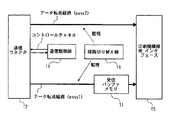
以下、本発明の1実施形態について図面を参照して説明する。図1は、実施形態のプリンタにおけるデータ転送経路の概要を表す図である。図では、セントロニクスパラレルやUSB(Universal Serial Bus)等の各種インタフェースを収用する通信コネクタ12と、印刷機構部30に対する窓口となる印刷機構部側インタフェース15との間におけるデータ転送の様子が表されている。印刷機構部側インタフェース15は、印刷データが存在する限り、常に印刷機構部30に対して単位データ(例えば1バイトのデータ)を提示している。印刷機構部30のデータ処理が順調であるときには、印刷機構部側インタフェース15から逐次単位データ(1バイト)が取り出されていく。
【0018】
実施形態におけるプリンタは、ホストコンピュータとの間でパケット通信を行なう。パケット制御のための通信制御部13は、コントロールチャネルを介してホストコンピュータと通信制御情報をやりとりする。この通信制御部13は、例えばASIC(Application Specified IC)のようなカスタムチップによって実現されるもので、その機能は従来のプリンタにおけるパケット制御機能と異ならない。
【0019】
パケット通信を用いてホストコンピュータと通信を行なう場合、以下のような手順がとられる。まず、コントロールチャネルを介して、ホストコンピュータから通信制御部13に対して受信可能データ量の問い合わせが行なわれる。これに対しプリンタは、受信バッファメモリ11の空き容量を調べ、通信制御部13が受信可能データ量をホストコンピュータに通知する。ホストコンピュータはデータチャネルを介して、通知を受けた分量のデータを一括して送信する。
【0020】
実施形態において特徴的な点は、入力コネクタ12から印刷機構部側インタフェース15に至るデータ転送経路が2通り(pass1及びpass2)設けられてあり、経路切り替え部14がデータ転送状況を監視しつつ、適切な経路を選択してデータを転送させることにある。この経路切り替え部14は、プリンタの統轄制御部20と、データ転送状況を監視するための専用チップとによって実現される機能のブロックである。
【0021】
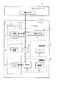
図2は、上記の経路切り替え部14が如何にして適切な経路を選択するのかの詳細を説明する図であり、専用チップ40が担う機能の内容が表されている。専用チップ40の入力側データセレクタ41は図1における通信コネクタ12に対して、また出力側データセレクタ45は図1における印刷機構部側インタフェース15に対して、各々接続されている。また、CPU22と(機能的にはプリンタの統轄制御部20と)通信を行なうためのCPUインタフェース44が設けられている。
【0022】
図中、実線の矢印で表されるのは2通りのデータ転送経路(pass1及びpass2)である。印刷データがいずれのデータ転送路を通過している場合にも、タイマー42が単位データ(1バイト)の通過する時間間隔を検知している。その情報はデータ転送状況判断部43に対して通知される。
【0023】
既に述べたように、印刷機構部30のデータ処理が順調であるときには、印刷機構部側インタフェース15から逐次単位データが(1バイト)取り出されていく。そのため、データ転送経路を通過していくデータの時間間隔も長くはならない。それに対して、印刷機構部30でのデータ処理に滞りが生じているときには、データ転送路内における単位データ(1バイト)の通過する時間間隔も長くなる。このような情報に基づいて、データ転送状況判断部43がプリンタ内部でのデータ転送に滞りが生じているか否かについて判断し、その旨をCPU22に対して報告する。CPU22は、その報告に基づいて何れのデータ転送路を用いるかを決定し、入力側データセレクタに指示を与える。
【0024】
図3には、以上のような判断手順等の具体的流れを表すフローチャートが描かれている。まず、プリンタの電源が投入されると、CPU22から専用チップ40のCPUインタフェース44を介して、入力側データセレクタ41に対してデータ転送経路の選択指示が与えられる(S101)。本実施形態では、プリンタ内部でのデータ転送速度の向上に主眼が置かれるため、電源投入後の初期状態では転送経路(pass2)が選択されるようにしている。この転送経路(pass2)は、通信コネクタ12と印刷機構部側インタフェース15との間のデータ転送に際して、受信バッファメモリ11を経由させずにデータを転送させるための経路である。なお、転送経路(pass2)においては、印刷データの転送にCPU22が直接関与することなく、いわゆるDMA(Direct Memory Access)転送が行なわれる。
【0025】
次に、データ転送状況判断部43の記憶部431に対して、タイムアウト時間の設定値が与えられ、記憶される(S102)。このタイムアウト時間は、タイマー42から通知されるデータ通過時間の間隔が、どれだけの大きさになったときにデータ転送に滞りが生じていると判断するかの資料とされる値である。なお、この値は、様々な印刷環境に応じて、異なる値を設定するようにしてもよい。例えば、高品質印刷を行なっているのか、あるいはドラフト印刷を行なっているのかによって、このタイムアウト時間の値を調整してやれば、より適切な条件でデータ転送滞りの判断が行なえることとなる。
【0026】
印刷データの受信が確認されると(S103においてYES)、タイマー42に対して、単位印刷データ(1バイト)の通過時間間隔の検出開始が指示される(S104)。検出に係る時間は、データ転送状況判断部43の比較部432に対して逐次通知される。この比較部432では、記憶部431に設定されているタイムアウト時間の値と、通知されてくる時間とを比較する。
【0027】
印刷機構部側に何らかの事情が発生し(例えば、テキスト印字が連続して機構部の駆動がデータ量に追いつかなくなったとき)、その結果、検出値が設定値を上回ると(S105においてYES)データ転送に滞りがあると判断され、その旨はCPUインタフェース44を介してCPU22に報告される。
【0028】
報告を受けたCPU22は、CPUインタフェース44を介して入力側データセレクタ41に対し、データ転送経路(pass1の1)を選択するよう指示が与えられる(S106)。これにより、CPU22は印刷データをPCIO転送によって受信バッファメモリ11に蓄積していく。それと同時に、出力側データセレクタ45は、転送路(pass1の2)から印刷データを受け入れる状態となって、CPU22によって受信バッファメモリ11から読み出され、送出されてくる単位データ(1バイト)を印刷機構部側インタフェース15に送り出す。
【0029】
図4には、上記のようなデータ転送に滞りが発生した状態での手続の流れについて説明するフローチャートが描かれている。既に述べたように、通信制御部13はホストコンピュータからの印刷データ受信に際して、一括して受信できるデータ量を応答している。従って、プリンタの統轄制御部20は、上記情報に基づいて、ホストコンピュータに対して応答した分量の印刷データ全てを受信バッファメモリ11に格納したか否かを確認できる(S201及びS202)。
【0030】
ホストコンピュータに応答した分の全ての印刷データを受信バッファメモリ11に格納し終えたら(S202においてYES)、入力側データセレクタ41を一旦アイソレーション状態とし、いずれの転送路(pass1及びpass2)をも選択していない状態となるように指示する(S203)。その後、受信バッファメモリ11に蓄積されている印刷データを、CPU22によって転送路(pass1の2)から出力し終えたら(S204においてYES)、再びホストコンピュータからのデータ受信及びプリンタ内部でのデータ転送を開始するため、CPU22は入力側データセレクタ41に対して、データ転送経路(pass2)を選択するよう指示が与えられる(S205)。また、出力側データセレクタ45も、転送路(pass2)からデータを受け入れる状態とされる(S206)。
【0031】
本実施形態は以上のとおりであるが、本発明は上記内容に拘らず、その要旨を逸脱しない範囲で様々な構成変更が可能である。特に、実施形態において受信バッファメモリ11は、プリンタ1が備えるDRAMモジュール2の所定のアドレス空間を割り当てて構成されるとしたが、この受信バッファメモリ11は専用の記憶素子を用いて構成されているものであってもよい。
【0032】
また、実施形態においては、監視に係るデータ転送状況に応じていずれかのデータ転送経路を選択して使用させるための機能のブロックである経路切り替え部14(図1)は、プリンタの統轄制御部20と専用チップ40が有する機能とが、相互に結びついてこれを実現しているが、これら機能は単独のカスタムチップのみに集約して担わせることも可能である。
【0033】
また、実施形態において、受信バッファメモリを経由させないデータ転送経路においてはデータのDMA転送を行なうものとして説明したが、これも通常のPCIO転送による構成としても構わない。
【0034】
【発明の効果】
従来のプリンタにおけるデータの内部転送に際しては、受信バッファメモリに対するデータの書込みや読み出しに、ある程度の時間が費やされることは不可避であった。本発明では、印刷データのサイズがある程度の大きさを有しており、それに対して印刷機構部の処理速度が十分に速いような場合には、受信バッファメモリを経由させずに印刷データの転送を行なわせることが可能となった。
【0035】
しかも、上記のような状態から何らかの理由によりデータ転送に滞りが生じたときには、従来通り印刷データを受信バッファメモリに経由させることもできる。そのため、例えばホストコンピュータとプリンタとがパケット通信を行なっている場合のように、そのデータ(パケット)の途中でデータ転送を中断させることができないような場合であっても、ホストコンピュータから送信されたデータが、確実にプリンタ側で受信されることが約束され、パケットの取りこぼしが生ずるなどの不都合が発生することもない。
【図面の簡単な説明】
【図1】実施形態のプリンタにおけるデータ転送経路の概要を表す図。
【図2】本発明の経路切り替え手段の主要部分を占める機能を表す図。
【図3】プリンタの電源を投入してから、データ転送に滞りが生じる事態に至る場合の制御手順について説明するフローチャート。
【図4】データ転送に滞りが生じた状態からの制御手順について説明するフローチャート。
【図5】受信バッファメモリを備えるプリンタにおけるデータの流れを表す図。
【符号の説明】
1 プリンタ
3 ホストコンピュータ
10 インタフェース部
11 受信バッファメモリ
12 通信コネクタ
13 通信制御部
14 経路切り替え部
15 印刷機構部側インタフェース
20 統轄制御部
22 CPU
30 印刷機構部
40 専用チップ
41 入力側データセレクタ
42 タイマー
43 データ転送状況判断部
431 記憶部
432 比較部
44 CPUインタフェース
45 出力側データセレクタ[0001]
BACKGROUND OF THE INVENTION
The present invention relates to a data transmission technique when print data received by a printer from a host computer is transmitted within the printer.
[0002]
[Prior art]
In recent printers, it is common to use a reception buffer memory as a buffer storage device in order to quickly release the host computer from operations related to printing, to improve the printing speed, or to transmit print data without stagnation. Is.
[0003]
FIG. 5 is a diagram illustrating a data flow in a printer including the reception buffer memory as described above.
[0004]
In FIG. 5, each function block of the
[0005]
The
[0006]
The interface unit 10 has a
[0007]
Incidentally, in recent years, the processing speed of the printing mechanism has been remarkably improved, but the data transfer processing speed inside the printer has not been improved so much. In particular, a DRAM module having a simple structure and a relatively low cost is generally used for the reception buffer memory. However, the DRAM is not a semiconductor memory having such a high speed. For this reason, in the mechanism in which data is temporarily stored in the reception buffer memory as described above, it cannot be avoided that a certain amount of time is spent for taking data in and out of the buffer memory.
[0008]
For example, when processing full-color graphic print data in an inkjet printer, if the data size is large, while the speed of the printing mechanism that processes it is sufficiently fast, only the time required to put data in and out of the receive buffer memory A delay occurs in the internal transfer of data, and a situation occurs in which the printing mechanism unit is waiting for data.
[0009]
[Problems to be solved by the invention]
In order to prevent such a situation from occurring, as shown by a dotted line (passs2) in FIG. 5, data that directly sends data to the
[0010]
In order to cope with various forms of printed documents without failure as described above, it can be said that the reception buffer memory as a buffer storage device is indispensable.
[0011]
The present invention has been made to overcome the above-described problems, and the object of the present invention is to achieve optimal printing conditions in various document forms in order to complete the printing process most quickly. An object of the present invention is to provide means for transferring data in a printer.
[0012]
[Means for Solving the Problems]
In order to solve the above problems, the present invention provides a case where print data input from a host computer is passed to the print mechanism unit via the reception buffer memory and a case where the print data is passed to the print mechanism unit without passing through the reception buffer memory. Depending on the situation, the route can be selected according to the situation.
[0013]
That is, the data transfer device in the printing apparatus according to
[0014]
According to a second aspect of the present invention, there is provided the data transfer apparatus in the printing apparatus according to the first aspect, wherein the data transfer path switching unit is configured to determine whether the data transfer state determination unit When there is no stagnation in the transfer of print data to the printer, the second data transfer path is selected, and when there is a stagnation in the transfer of print data to the printing mechanism unit, the first data transfer path is selected. It is characterized by that.
[0015]
A data transfer method in the printing apparatus for solving the above problem is as follows. That is, in the data transfer method according to the third aspect, when the print data received from the host computer is transferred to the print mechanism unit in the printing apparatus, the received print data is temporarily stored in the reception buffer memory. A first data transfer method for transferring data to the printing mechanism unit after the data has been accumulated and a second data transfer method for transferring data directly to the printing mechanism unit without going through the reception buffer memory. This is a data transfer method adopted in the above. Then, the second data transfer method is employed when there is no stagnation in the transfer of the print data to the printing mechanism unit, and the first data transfer method is employed when the transfer of the print data to the printing mechanism unit is stagnation. Is used to transfer data.
[0016]
The computer program for realizing the print data transfer control procedure in the printing apparatus can be recorded and held in a specific medium. That is, the recording medium storing the program according to claim 4 includes: a first data transfer path for transferring print data received from a host computer to a printing mechanism unit via a reception buffer memory; and the reception buffer. A program for controlling a printer comprising a second data transfer path for direct transfer to the printing mechanism without passing through a memory, wherein the data transfer path switching means transfers data to the printing mechanism. The control content is to switch the print data transfer path to the print mechanism unit to the first or second data transfer path based on the determination result of the status determination means.
[0017]
DETAILED DESCRIPTION OF THE INVENTION
Hereinafter, an embodiment of the present invention will be described with reference to the drawings. FIG. 1 is a diagram illustrating an outline of a data transfer path in the printer of the embodiment. The figure shows a state of data transfer between the
[0018]
The printer in the embodiment performs packet communication with a host computer. The
[0019]
When communicating with a host computer using packet communication, the following procedure is taken. First, an inquiry about the receivable data amount is made from the host computer to the
[0020]
A characteristic point in the embodiment is that two data transfer paths (pass1 and pass2) from the
[0021]
FIG. 2 is a diagram for explaining in detail how the
[0022]
In the figure, two data transfer paths (pass1 and pass2) are represented by solid arrows. When the print data passes through any data transfer path, the
[0023]
As described above, when the data processing of the
[0024]
FIG. 3 is a flowchart showing a specific flow of the determination procedure and the like as described above. First, when the printer is turned on, a data transfer path selection instruction is given from the CPU 22 to the input side data selector 41 via the
[0025]
Next, a set value for the timeout time is given to the
[0026]
When the reception of the print data is confirmed (YES in S103), the
[0027]
If some situation occurs on the printing mechanism unit side (for example, when text printing continues and the driving of the mechanism unit cannot catch up with the data amount), and the detection value exceeds the set value as a result (YES in S105), the data It is determined that there is a delay in the transfer, and that fact is reported to the CPU 22 via the
[0028]
Receiving the report, the CPU 22 is instructed to select the data transfer path (1 of pass1) to the input side data selector 41 via the CPU interface 44 (S106). As a result, the CPU 22 accumulates print data in the
[0029]
FIG. 4 is a flowchart for explaining the flow of the procedure in the state where the data transfer is delayed as described above. As already described, the
[0030]
When all the print data corresponding to the host computer has been stored in the reception buffer memory 11 (YES in S202), the input side data selector 41 is once set in the isolation state, and any transfer path (pass1 and pass2) is set. An instruction is given to enter a state of not being selected (S203). Thereafter, when the CPU 22 finishes outputting the print data stored in the
[0031]
Although the present embodiment is as described above, the present invention can be modified in various ways without departing from the gist of the present invention regardless of the above contents. In particular, in the embodiment, the
[0032]
In the embodiment, the path switching unit 14 (FIG. 1), which is a function block for selecting and using any data transfer path according to the data transfer status related to the monitoring, is a printer control unit. 20 and the functions of the
[0033]
Further, in the embodiment, the data transfer path that does not pass through the reception buffer memory is described as performing the DMA transfer of the data. However, this may be configured by a normal PCIO transfer.
[0034]
【The invention's effect】
In internal transfer of data in a conventional printer, it is inevitable that a certain amount of time is spent in writing and reading data to and from the reception buffer memory. In the present invention, when the size of the print data has a certain size and the processing speed of the printing mechanism is sufficiently fast, the transfer of the print data without going through the reception buffer memory. It has become possible to perform.
[0035]
In addition, when data transfer is delayed for some reason from the above state, the print data can be passed through the reception buffer memory as usual. Therefore, even when the data transfer cannot be interrupted in the middle of the data (packet), for example, when the host computer and the printer are performing packet communication, they are transmitted from the host computer. It is promised that the data is surely received by the printer, and there is no inconvenience such as packet dropping.
[Brief description of the drawings]
FIG. 1 is a diagram illustrating an outline of a data transfer path in a printer according to an embodiment.
FIG. 2 is a diagram showing functions that occupy the main part of the route switching means of the present invention.
FIG. 3 is a flowchart for explaining a control procedure in a case where a delay occurs in data transfer after the printer is turned on.
FIG. 4 is a flowchart for explaining a control procedure from a state in which data transfer is delayed.
FIG. 5 is a diagram illustrating a data flow in a printer including a reception buffer memory.
[Explanation of symbols]
DESCRIPTION OF
30
Claims (5)
前記受信バッファメモリを経由することなく、前記印刷機構部へ直接転送する第2のデータ転送経路と、
を有する印刷装置において、
電源投入後の初期状態では前記第2のデータ転送経路を選択する手段と、
前記印刷データの単位データが前記第2のデータ転送経路を通過する時間間隔を検知する手段と、
前記時間間隔を所定のタイムアウト時間と比較し、前記時間間隔が前記タイムアウト時間を上回っている場合、前記第2のデータ転送経路から前記第1のデータ転送経路に切り替え、前記第1のデータ転送経路で前記印刷データの転送を行う切り替え手段と
を有することを特徴とする印刷装置。A first data transfer path for temporarily storing the print data received from the host computer in the reception buffer memory and then transferring the print data to the print mechanism unit;
A second data transfer path for transferring directly to the printing mechanism without going through the reception buffer memory;
In a printing apparatus having
Means for selecting the second data transfer path in an initial state after power-on;
Means for detecting a time interval during which the unit data of the print data passes through the second data transfer path ;
The time interval is compared with a predetermined time-out period, if the time interval exceeds the time-out period, the switching from the second data transfer path to said first data transfer path, said first data transfer path Switching means for transferring the print data in
Printing apparatus characterized by having a.
前記受信バッファメモリを経由することなく、前記印刷機構部へ直接転送する第2のデータ転送経路と、
を有する印刷装置の印刷方法において、
電源投入後の初期状態では前記第2のデータ転送経路が選択され、
前記印刷データの単位データが前記第2のデータ転送経路を通過する時間間隔を検知し、前記時間間隔を所定のタイムアウト時間と比較し、前記時間間隔が前記タイムアウト時間を上回っている場合、前記第2のデータ転送経路から前記第1のデータ転送経路に切り替えられ、前記第1のデータ転送経路で前記印刷データの転送を行うことを特徴とする印刷方法。When the print data received from the host computer is transferred to the print mechanism within the printing apparatus, the received print data is temporarily stored in the reception buffer memory and then transferred to the print mechanism. A first data transfer path to
A second data transfer path for transferring directly to the printing mechanism without going through the reception buffer memory;
In the printing method of the printing apparatus having
In the initial state after power-on, the second data transfer path is selected,
If the unit data of the print data to detect the time interval that passes through the second data transfer path, the time interval is compared with a predetermined time-out period, the time interval is greater than the time-out period, the first is switched from the second data transfer path to said first data transfer path, a printing method, characterized in that the transfer of the print data in said first data transfer path.
前記受信バッファメモリを経由することなく、前記印刷機構部へ直接転送する第2のデータ転送経路と、
を有する印刷装置のデータ転送を制御するプログラムにおいて、
電源投入後の初期状態で前記第2のデータ転送経路を選択する手順、
前記印刷データの単位データが前記第2のデータ転送経路を通過する時間間隔を検知する手順、
前記時間間隔を所定のタイムアウト時間と比較する手順、
前記時間間隔が前記タイムアウト時間を上回っている場合、前記第2のデータ転送経路から前記第1のデータ転送経路に切り替え、前記第1のデータ転送経路で前記印刷データを転送させる手順
を前記印刷装置に実行させることを特徴とするプログラム。A first data transfer path for transferring print data received from the host computer to the printing mechanism after passing through the reception buffer memory;
A second data transfer path for transferring directly to the printing mechanism without going through the reception buffer memory;
In a program for controlling data transfer of a printing apparatus having
A procedure for selecting the second data transfer path in an initial state after power-on;
A procedure for detecting a time interval during which the unit data of the print data passes through the second data transfer path ;
Comparing the time interval with a predetermined timeout period;
A procedure for switching from the second data transfer path to the first data transfer path and transferring the print data through the first data transfer path when the time interval exceeds the timeout time
That causes the printing apparatus to execute the program .
Priority Applications (1)
| Application Number | Priority Date | Filing Date | Title |
|---|---|---|---|
| JP2002093388A JP4529341B2 (en) | 2002-03-28 | 2002-03-28 | Printing apparatus, printing method, and program |
Applications Claiming Priority (1)
| Application Number | Priority Date | Filing Date | Title |
|---|---|---|---|
| JP2002093388A JP4529341B2 (en) | 2002-03-28 | 2002-03-28 | Printing apparatus, printing method, and program |
Publications (3)
| Publication Number | Publication Date |
|---|---|
| JP2003285478A JP2003285478A (en) | 2003-10-07 |
| JP2003285478A5 JP2003285478A5 (en) | 2005-09-15 |
| JP4529341B2 true JP4529341B2 (en) | 2010-08-25 |
Family
ID=29237869
Family Applications (1)
| Application Number | Title | Priority Date | Filing Date |
|---|---|---|---|
| JP2002093388A Expired - Fee Related JP4529341B2 (en) | 2002-03-28 | 2002-03-28 | Printing apparatus, printing method, and program |
Country Status (1)
| Country | Link |
|---|---|
| JP (1) | JP4529341B2 (en) |
Families Citing this family (4)
| Publication number | Priority date | Publication date | Assignee | Title |
|---|---|---|---|---|
| JP4753532B2 (en) * | 2003-08-27 | 2011-08-24 | 株式会社沖データ | Image forming apparatus |
| JP2007155765A (en) * | 2005-11-30 | 2007-06-21 | Ricoh Co Ltd | Image forming apparatus, communication method, and communication program |
| JP4736927B2 (en) | 2006-04-21 | 2011-07-27 | ブラザー工業株式会社 | Information processing apparatus, image forming system, and device driver program |
| JP6696234B2 (en) * | 2016-03-11 | 2020-05-20 | 株式会社リコー | Image forming apparatus, image processing method, and program |
Citations (2)
| Publication number | Priority date | Publication date | Assignee | Title |
|---|---|---|---|---|
| JP2000259362A (en) * | 1999-03-10 | 2000-09-22 | Seiko Epson Corp | Printer and data processing method of printer |
| JP2002011925A (en) * | 2001-05-22 | 2002-01-15 | Seiko Epson Corp | Printer, its controlling method and medium recording program |
Family Cites Families (1)
| Publication number | Priority date | Publication date | Assignee | Title |
|---|---|---|---|---|
| JPH0958064A (en) * | 1995-08-25 | 1997-03-04 | Brother Ind Ltd | Terminal device |
-
2002
- 2002-03-28 JP JP2002093388A patent/JP4529341B2/en not_active Expired - Fee Related
Patent Citations (2)
| Publication number | Priority date | Publication date | Assignee | Title |
|---|---|---|---|---|
| JP2000259362A (en) * | 1999-03-10 | 2000-09-22 | Seiko Epson Corp | Printer and data processing method of printer |
| JP2002011925A (en) * | 2001-05-22 | 2002-01-15 | Seiko Epson Corp | Printer, its controlling method and medium recording program |
Also Published As
| Publication number | Publication date |
|---|---|
| JP2003285478A (en) | 2003-10-07 |
Similar Documents
| Publication | Publication Date | Title |
|---|---|---|
| US6434643B1 (en) | Transmission of status information by a selected one of multiple transfer modes based on the cause for sending the status information | |
| JP3565567B2 (en) | Switching device and method for sharing peripheral device | |
| US8392630B2 (en) | Information processing apparatus having first DMA controller and second DMA controller wherein selection circuit determines which DMA will perform data transfer based on higher data transfer performance | |
| JP4529341B2 (en) | Printing apparatus, printing method, and program | |
| US5926650A (en) | Method and system utilizing a negotiation phase to transfer commands and data in separate modes over a host/peripheral interface | |
| JP4474873B2 (en) | Image processing device | |
| US20050198428A1 (en) | Interface apparatus and image forming apparatus | |
| JP5701034B2 (en) | Data processing apparatus, data processing apparatus control method, and program | |
| JP6833491B2 (en) | Information processing device | |
| JP4948357B2 (en) | Image forming apparatus and print job protection method | |
| JP2002019212A (en) | Printer | |
| US20180213103A1 (en) | Image processing apparatus, method of controlling the same, and storage medium | |
| US8671251B2 (en) | Information processing apparatus that executes response process to received information, control method therefor, and storage medium storing control program therefor | |
| JP4400097B2 (en) | Printing apparatus, printing control method, program, and recording medium | |
| JP2009006570A (en) | Printer | |
| JP2001142670A (en) | Printing system and printer | |
| US11010111B2 (en) | Image forming apparatus including a constant log storage | |
| KR100334111B1 (en) | Method for canceling of printing job | |
| JP4829733B2 (en) | Image processing apparatus and image processing method | |
| JP2004165741A (en) | Image processor | |
| US6295135B1 (en) | Release of busy signal when free capacity of a reception buffer exceeds a predetermined amount | |
| JP2007210279A (en) | Data processor, printer, and control method | |
| JP5580584B2 (en) | PRINT CONTROL DEVICE, CONTROL METHOD FOR PRINT CONTROL DEVICE, AND PROGRAM | |
| JP2004148695A (en) | Printer performing automatic printing according to print information file | |
| JP2007021809A (en) | Method for controlling printing image data in color four-d printer |
Legal Events
| Date | Code | Title | Description |
|---|---|---|---|
| A521 | Written amendment |
Free format text: JAPANESE INTERMEDIATE CODE: A523 Effective date: 20050328 |
|
| A621 | Written request for application examination |
Free format text: JAPANESE INTERMEDIATE CODE: A621 Effective date: 20050328 |
|
| RD03 | Notification of appointment of power of attorney |
Free format text: JAPANESE INTERMEDIATE CODE: A7423 Effective date: 20071228 |
|
| A131 | Notification of reasons for refusal |
Free format text: JAPANESE INTERMEDIATE CODE: A131 Effective date: 20090127 |
|
| A521 | Written amendment |
Free format text: JAPANESE INTERMEDIATE CODE: A523 Effective date: 20090310 |
|
| A131 | Notification of reasons for refusal |
Free format text: JAPANESE INTERMEDIATE CODE: A131 Effective date: 20090721 |
|
| A521 | Written amendment |
Free format text: JAPANESE INTERMEDIATE CODE: A523 Effective date: 20090916 |
|
| A131 | Notification of reasons for refusal |
Free format text: JAPANESE INTERMEDIATE CODE: A131 Effective date: 20100209 |
|
| A521 | Written amendment |
Free format text: JAPANESE INTERMEDIATE CODE: A523 Effective date: 20100406 |
|
| TRDD | Decision of grant or rejection written | ||
| A01 | Written decision to grant a patent or to grant a registration (utility model) |
Free format text: JAPANESE INTERMEDIATE CODE: A01 Effective date: 20100518 |
|
| A01 | Written decision to grant a patent or to grant a registration (utility model) |
Free format text: JAPANESE INTERMEDIATE CODE: A01 |
|
| A61 | First payment of annual fees (during grant procedure) |
Free format text: JAPANESE INTERMEDIATE CODE: A61 Effective date: 20100531 |
|
| R150 | Certificate of patent or registration of utility model |
Free format text: JAPANESE INTERMEDIATE CODE: R150 |
|
| FPAY | Renewal fee payment (event date is renewal date of database) |
Free format text: PAYMENT UNTIL: 20130618 Year of fee payment: 3 |
|
| FPAY | Renewal fee payment (event date is renewal date of database) |
Free format text: PAYMENT UNTIL: 20130618 Year of fee payment: 3 |
|
| S531 | Written request for registration of change of domicile |
Free format text: JAPANESE INTERMEDIATE CODE: R313531 |
|
| R350 | Written notification of registration of transfer |
Free format text: JAPANESE INTERMEDIATE CODE: R350 |
|
| LAPS | Cancellation because of no payment of annual fees |