JP4527552B2 - Semiconductor device and manufacturing method thereof - Google Patents
Semiconductor device and manufacturing method thereof Download PDFInfo
- Publication number
- JP4527552B2 JP4527552B2 JP2005008855A JP2005008855A JP4527552B2 JP 4527552 B2 JP4527552 B2 JP 4527552B2 JP 2005008855 A JP2005008855 A JP 2005008855A JP 2005008855 A JP2005008855 A JP 2005008855A JP 4527552 B2 JP4527552 B2 JP 4527552B2
- Authority
- JP
- Japan
- Prior art keywords
- fin
- type semiconductor
- source
- insulating film
- semiconductor region
- Prior art date
- Legal status (The legal status is an assumption and is not a legal conclusion. Google has not performed a legal analysis and makes no representation as to the accuracy of the status listed.)
- Expired - Fee Related
Links
Images


Classifications
-
- H—ELECTRICITY
- H10—SEMICONDUCTOR DEVICES; ELECTRIC SOLID-STATE DEVICES NOT OTHERWISE PROVIDED FOR
- H10D—INORGANIC ELECTRIC SEMICONDUCTOR DEVICES
- H10D30/00—Field-effect transistors [FET]
- H10D30/60—Insulated-gate field-effect transistors [IGFET]
- H10D30/62—Fin field-effect transistors [FinFET]
-
- H—ELECTRICITY
- H10—SEMICONDUCTOR DEVICES; ELECTRIC SOLID-STATE DEVICES NOT OTHERWISE PROVIDED FOR
- H10D—INORGANIC ELECTRIC SEMICONDUCTOR DEVICES
- H10D30/00—Field-effect transistors [FET]
- H10D30/01—Manufacture or treatment
- H10D30/021—Manufacture or treatment of FETs having insulated gates [IGFET]
- H10D30/024—Manufacture or treatment of FETs having insulated gates [IGFET] of fin field-effect transistors [FinFET]
-
- H—ELECTRICITY
- H10—SEMICONDUCTOR DEVICES; ELECTRIC SOLID-STATE DEVICES NOT OTHERWISE PROVIDED FOR
- H10D—INORGANIC ELECTRIC SEMICONDUCTOR DEVICES
- H10D30/00—Field-effect transistors [FET]
- H10D30/60—Insulated-gate field-effect transistors [IGFET]
- H10D30/62—Fin field-effect transistors [FinFET]
- H10D30/6219—Fin field-effect transistors [FinFET] characterised by the source or drain electrodes
Landscapes
- Thin Film Transistor (AREA)
Description
本発明は、半導体装置とその製造方法に関し、特にフィン型構造を持つ電界効果トランジスタを含む半導体装置とその製造方法に関する。 The present invention relates to a semiconductor device and a manufacturing method thereof, and more particularly to a semiconductor device including a field effect transistor having a fin-type structure and a manufacturing method thereof.
なお、フィン型構造を持つ電界効果トランジスタとは、一般的にFin−FETまたはダブルゲートFin−FETと呼ばれ、基板の表面に対してチャネルの面が垂直になっている3次元型の電界効果トランジスタであって、基板の面に対して垂直な薄い壁(フィン)状の突起があり、フィンの両側面上にゲート絶縁膜、ゲート電極が形成され、ゲート両側のフィンにソース/ドレイン領域が形成されている構造を有する。 Note that a field effect transistor having a fin-type structure is generally called a Fin-FET or a double-gate Fin-FET, and a three-dimensional field effect in which the channel surface is perpendicular to the surface of the substrate. A transistor having thin wall (fin) projections perpendicular to the surface of the substrate, a gate insulating film and a gate electrode are formed on both side surfaces of the fin, and source / drain regions are formed on the fins on both sides of the gate. It has a formed structure.
フィン型構造を持つ電界効果トランジスタは、チャネル面を基板表面に垂直に配置するため、基板上の占有面積を低減でき、誘電体分離を容易とし、微細化、高速動作化に対する適応性が高い。絶縁膜上にシリコン層を配置したSOI(semiconductor on insulator)基板のシリコン層上に酸化膜や、酸化膜/窒化膜積層等のキャップ層を設け、パターニングしてシリコンのフィンを形成する。フィン表面に酸化シリコン、窒化酸化シリコン等のゲート絶縁膜を形成した後、ポリシリコン層を堆積し、パターニングして絶縁ゲート電極を形成する。ゲート電極両側のフィン領域をドープしてソース/ドレイン領域を形成すれば、基本的なFET構造を形成できる。 A field effect transistor having a fin-type structure has a channel surface arranged perpendicular to the substrate surface, so that the occupied area on the substrate can be reduced, dielectric separation is facilitated, and adaptability to miniaturization and high-speed operation is high. An oxide film or a cap layer such as an oxide film / nitride film stack is provided on a silicon layer of an SOI (semiconductor on insulator) substrate in which a silicon layer is arranged on an insulating film, and patterned to form silicon fins. After forming a gate insulating film such as silicon oxide or silicon nitride oxide on the fin surface, a polysilicon layer is deposited and patterned to form an insulated gate electrode. If the source / drain regions are formed by doping the fin regions on both sides of the gate electrode, a basic FET structure can be formed.
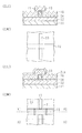
Fin−FETの構成例を、図5に示す。図5において、SOI基板のシリコン層をパターニングして、フィン51とその両側で幅を広げたコンタクト領域52,53が形成される。シリコン層の上にはキャップ層61が残る。フィン側壁に犠牲酸化膜を形成し、除去した後ゲート絶縁膜62を酸化、窒化などにより形成する。基板上にポリシリコン層を堆積し、パターニングしてゲート電極71を形成する。ゲート電極71の端部には幅を広げたコンタクト領域72が形成される。イオン注入などで不純物を添加してソース/ドレインを形成する。層間絶縁膜でトランジスタ構造を埋め込んだ後、コンタクト領域に達するコンタクトホールを開口し、タングステンプラグ等の導電性プラグ80をコンタクトホール内に埋め込む。ゲート電極をポリシリコン層とシリサイド層の積層とすることによりゲート抵抗を低減化することもできる。
本発明の目的は、高性能の、フィン型構造を持つ電界効果トランジスタを含む半導体装置とその製造方法を提供することである。 An object of the present invention is to provide a semiconductor device including a high-performance field effect transistor having a fin-type structure and a method for manufacturing the same.
本発明の他の目的は、ソース/ドレインのコンタクト抵抗が低い、フィン型構造を持つ電界効果トランジスタを含む半導体装置とその製造方法を提供することである。 Another object of the present invention is to provide a semiconductor device including a field effect transistor having a fin-type structure with a low source / drain contact resistance and a method for manufacturing the same.
本発明の一観点によれば、
絶縁性表面を有する支持基板と、
前記支持基板上に形成され、支持基板表面に対してほぼ垂直な一対の側面および前記両側面を接続する上面を有し、第1導電型を有するフィン型半導体領域と、
前記フィン型半導体領域の中間部を横断して形成され、ゲート絶縁膜とその上に形成された導電性ゲート電極とを含む絶縁ゲート電極構造と、
前記導電性ゲート電極両側の前記フィン型半導体領域に第2導電型不純物を添加して形成された、第2導電型を有するソース/ドレイン領域と、
前記導電性ゲート電極の側壁上に形成された第1サイドウォール絶縁膜と、前記フィン型半導体領域の側壁上に形成され、前記ソース/ドレイン領域上において、前記フィン型半導体領域の側面の上端から下端に達する開口を有する第2サイドウォール絶縁膜と、を含むサイドウォール絶縁膜と、
前記サイドウォール絶縁膜の開口内に露出された前記ソース/ドレイン領域の表面に形成されたシリサイド層と、
前記シリサイド層にコンタクトするソース/ドレイン電極と、
前記フィン型半導体領域、前記絶縁ゲート電極構造を埋め込み、前記サイドウォール絶縁膜の開口を露出するコンタクトホールを有する層間絶縁膜と、
を有し、前記シリサイド層は前記コンタクトホール内に形成されている半導体装置
が提供される。
According to one aspect of the present invention,
A support substrate having an insulating surface;
A fin-type semiconductor region having a first conductivity type, formed on the support substrate, having a pair of side surfaces substantially perpendicular to the support substrate surface and an upper surface connecting the both side surfaces;
The formed across the middle portion of the fin-type semiconductor region, a gate insulating film and including insulation gate electrode structure and a formed conductive gate electrode thereon,
A source / drain region having a second conductivity type formed by adding a second conductivity type impurity to the fin-type semiconductor region on both sides of the conductive gate electrode;
A first sidewall insulating film formed on the sidewall of the conductive gate electrode and a sidewall of the fin-type semiconductor region, and from the upper end of the side surface of the fin-type semiconductor region on the source / drain region A side wall insulating film including a second side wall insulating film having an opening reaching the lower end;
A silicide layer formed on the surface of the source / drain region exposed in the opening of the sidewall insulating film;
Source / drain electrodes in contact with the silicide layer;
An interlayer insulating film having a contact hole that embeds the fin-type semiconductor region and the insulating gate electrode structure and exposes an opening of the sidewall insulating film;
There is provided a semiconductor device in which the silicide layer is formed in the contact hole .
本発明の他の観点によれば、
(a)SOI基板の半導体層をパターニングし、絶縁表面を有する支持基板上に、支持基板表面に対しほぼ垂直な一対の側面および前記両側面を接続する上面を有するフィン型半導体領域を形成する工程と、
(b)前記フィン型半導体領域の中間部を横断し、ゲート絶縁膜とその上の導電性ゲート電極とを含む絶縁ゲート電極構造を形成する工程と、
(c)前記フィン型半導体領域および前記絶縁ゲート電極構造の側面上にサイドウォール絶縁膜を形成する工程と、
(d)前記絶縁ゲート電極構造両側の前記フィン型半導体領域にソース/ドレイン領域を形成する工程と、
(e)前記サイドウォール絶縁膜を覆って、層間絶縁膜を堆積する工程と、
(f)前記層間絶縁膜を貫通して前記ソース/ドレイン領域に達するコンタクトホールを開口すると共に、前記コンタクトホール内の前記サイドウォール絶縁膜を除去し、前記ソース/ドレイン領域を露出する工程と、
(g)前記コンタクトホール内に露出した前記ソース/ドレイン領域にシリサイド層を形成する工程と、
を含む半導体装置の製造方法
が提供される。
According to another aspect of the invention,
(A) A step of patterning a semiconductor layer of an SOI substrate to form a fin-type semiconductor region having a pair of side surfaces substantially perpendicular to the support substrate surface and an upper surface connecting the both side surfaces on the support substrate having an insulating surface. When,
(B) across the intermediate portion of the fin-type semiconductor region, a step of a conductive gate electrode thereon a gate insulating film to form a including insulation gate electrode structure,
(C) forming a sidewall insulating film on a side surface of the fin-type semiconductor region and the insulated gate electrode structure;
(D) forming source / drain regions in the fin-type semiconductor regions on both sides of the insulated gate electrode structure;
(E) depositing an interlayer insulating film so as to cover the sidewall insulating film;
(F) opening a contact hole that reaches the source / drain region through the interlayer insulating film, removing the sidewall insulating film in the contact hole, and exposing the source / drain region;
(G) forming a silicide layer in the source / drain region exposed in the contact hole;
A method for manufacturing a semiconductor device is provided.
ゲート電極の側面上にサイドウォール絶縁膜を形成しつつ、ソース/ドレイン領域のコンタクト部分ではサイドウォール絶縁膜を除去し、シリコン層の側面にシリサイド層を形成するため、ソース/ドレインのコンタクト抵抗を低減化できる。 While forming a sidewall insulating film on the side surface of the gate electrode, the sidewall insulating film is removed at the contact portion of the source / drain region, and a silicide layer is formed on the side surface of the silicon layer. It can be reduced.
以下、図面を参照して本発明の実施例を説明する。 Embodiments of the present invention will be described below with reference to the drawings.
図1A−1Yは、本発明の実施例によるフィン型構造を持つ電界効果トランジスタを含む半導体装置の製造方法を説明するための断面図、平面図、及び斜視図である。 1A- 1Y are a cross-sectional view, a plan view, and a perspective view for explaining a method of manufacturing a semiconductor device including a field effect transistor having a fin-type structure according to an embodiment of the present invention.
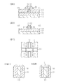
図1Aに示すように、シリコン支持基板11の上に、埋め込み酸化シリコン層12を設け、その上に薄いシリコン層13を備えたSOI基板を準備する。半導体素子を形成するシリコン層13は、例えば厚さ100nmに調整する。このシリコン層の厚さは、後に形成するフィン型領域の高さとなり、フィン型電界効果トランジスタのチャネル幅を決定する。
As shown in FIG. 1A, an SOI substrate provided with a buried
図1Bに示すように、N2、NO、NH3、NF3、N2O、エレクトロンサイクロトロンレゾナンス(ECR)プラズマで活性化した窒素雰囲気等の窒化性雰囲気中でSOI基板を800℃〜1000℃に加熱し、5分〜60分のアニールを行なう。シリコン層13と埋め込み酸化膜12との界面に窒化シリコン膜14xが形成されると共に、シリコン層13の表面にも窒化シリコン層14yが形成される。窒化シリコン層14xは、エッチストッパとしての機能を有する。なお、窒化性雰囲気中での熱処理に関しては、特開2002−26299号公報、段落0016〜0026を参照できる。
As shown in FIG. 1B, the SOI substrate is 800 ° C. to 1000 ° C. in a nitriding atmosphere such as a nitrogen atmosphere activated by N 2 , NO, NH 3 , NF 3 , N 2 O, electron cyclotron resonance (ECR) plasma. And anneal for 5 to 60 minutes. A silicon nitride film 14 x is formed at the interface between the
図1C1に示すように、表面の窒化シリコン層14yを熱燐酸等により除去する。 As shown in FIG. 1C1, the silicon nitride layer 14y on the surface is removed with hot phosphoric acid or the like.
図1C2に示すように、シリコン層13の上に、酸化シリコン層と窒化シリコン層との積層等のキャップ層CLを形成することもできる。なお、図1Bに示す窒化シリコン層14yをそのままキャップ層として用いても良い。以下、主にキャップ層CLがない構造を例にとって説明するが、キャップ層CLを設けた場合についても適宜説明する。
図1Dに示すように、シリコン層13の上に酸化シリコン層15を例えば厚さ10nm〜20nmCVDにより堆積し、ハードマスク層を形成する。酸化シリコン層15の上に、レジストマスクRM1を形成する。このレジストマスクRM1は、シリコン層13をエッチしてフィンを形成するためのマスクである。フィンの幅は、例えば約20nmである。レジストマスクRM1をエッチングマスクとし、ハードマスク層15をエッチングする。続いて、レジストマスクRM1及びハードマスク層15をマスクとしてシリコン層13をエッチングする。
As shown in FIG. 1C2, a cap layer CL such as a stacked layer of a silicon oxide layer and a silicon nitride layer can be formed on the
As shown in FIG. 1D, a
図1Eに示すように、レジストマスクRM1の形状にならってシリコン層13がエッチングされる。シリコン層13下の窒化シリコン層14は、エッチングストッパとして機能する。
As shown in FIG. 1E, the
図1Fに示すように、酸系の溶液を用い、レジストマスクRM1及びハードマスク層15を溶液洗浄により除去する。
As shown in FIG. 1F, using an acid-based solution, the resist mask RM1 and the
図1G1に示すように、800℃〜1200℃の温度で酸素を含むガス中で酸化処理を行なうことにより、シリコン層13表面に厚さ0.6nm〜2nmのゲート絶縁膜を形成する。その後、800℃〜1200℃の温度で窒素を含むガス中で窒化処理を行なうことにより、ゲート絶縁膜を酸窒化膜とする。窒素を含むガスとしては、上述同様のN2、NO、NH3、NF3、N2O、エレクトロンサイクロトロンレゾナンス(ECR)プラズマで活性化した窒素雰囲気等の窒化性雰囲気等を用いればよい。
このようにして、シリコン層13の上面及び側面に酸窒化膜のゲート絶縁膜15が形成される。
As shown in FIG. 1G1, by performing oxidation treatment in a gas containing oxygen at a temperature of 800 ° C. to 1200 ° C., a gate insulating film having a thickness of 0.6 nm to 2 nm is formed on the surface of the
In this manner, an oxynitride
図1G2に示すように、キャップ層CLがある場合は、ゲート絶縁膜15はシリコン層13の両側面にのみ形成される。
As shown in FIG. 1G2, when the cap layer CL is present, the
図1Hに示すように、フィン型構造を覆ってポリシリコン層16を厚さ約100nmCVDにより堆積する。フィン型半導体領域上およびその近傍では、ポリシリコン層16の高さは約200nmとなる。
As shown in FIG. 1H, a
図1Iに示すように、ポリシリコン16の上に、厚さ10nm〜20nmの酸化シリコン層17をCVDにより形成し、上述同様のハードマスク層を形成する。酸化シリコン層17の上にポリシリコン層16をエッチングするためのレジストマスクRM2を形成する。レジストマスクRM2は、ゲート電極をエッチングするためのマスクであり、ゲート長を決定するその幅は、100nm以下、例えば50nmとする。レジストマスクRM2をマスクとし、ハードマスク層17をエッチングし、レジストマスクRM2とハードマスク層17をマスクとしてポリシリコン層16をエッチングする。その後、酸系の溶液洗浄によりレジストマスクRM2及びハードマスク層17を除去する。
図1J、1Kに示すように、フィン型半導体領域13の中間部を横断するポリシリコンのゲート電極16が形成される。図1Jはゲート電極を通る断面図であり、図1Kは、ゲート電極16を形成した状態の平面図である。幅約20nmのフィン型半導体領域13の中間部を横断して、幅約50nmのポリシリコンゲート電極16が形成されている。
As shown in FIG. 1I, a silicon oxide layer 17 having a thickness of 10 nm to 20 nm is formed on
As shown in FIGS. 1J and 1K, a
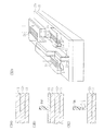
図1Lに示すように、基板全面上に厚さ10nm〜20nmの酸化シリコン層21pをCVDにより堆積する。続いてリアクティブイオンエッチング(RIE)を行ない、平坦部上の酸化シリコン層21pを除去する。酸化シリコン層21pは、基板表面に対してほぼ垂直な側面上にのみ残る。
As shown in FIG. 1L, a
図1M、1N、1Oが酸化シリコンのサイドウォール21を形成した状態の平面図及びX1−X1方向及びX2−X2方向の断面図である。ゲート電極16およびフィン型半導体領域の側壁上に酸化シリコンのサイドウォールが形成されている。
1M, 1N, and 1O are a plan view and a cross-sectional view in the X1-X1 direction and the X2-X2 direction in a state where the
図1Pに示すように、フィン型シリコン領域13に対して斜め方向からイオン注入を行ない、ソース/ドレイン領域のエクステンション、高濃度領域を形成する。必要に応じて逆導電型のポケット領域をイオン注入してもよい。なお、これらのイオン注入は、公知の方法で行なえばよい。例えば、サイドウォール絶縁膜21を作る前にエクステンションとポケットのイオン注入を行い、サイドウォール21を作成した後高濃度領域のイオン注入を行なっても良い。
As shown in FIG. 1P, ions are implanted into the fin-
図1Q1は、キャップ層がない場合のフィン型シリコン領域13に形成されたソース/ドレイン領域18の断面形状を示す。nチャネルMOSトランジスタの場合、p型のフィン型シリコン領域13の上面及び両側面にn型のソース/ドレイン領域18が形成される。
FIG. 1Q1 shows a cross-sectional shape of the source /
図1Q2は、キャップ層CLを有する場合の形状を示す。フィン型シリコン領域13の両側面にのみソース/ドレイン領域18が形成されている。イオン注入後、800℃〜1200℃の温度でアニールし、イオン注入した不純物を活性化する。
FIG. 1Q2 shows the shape when the cap layer CL is provided. Source /
以上の工程により、フィン型シリコン領域13を横切ってポリシリコンのゲート電極16が形成され、ポリシリコンゲート電極16の両側にソース/ドレイン領域が形成されて基本的なFET構造が作成される。
Through the above steps, a
図1R、1S、1Tは、フィン型FET構造を覆って酸化シリコン膜、PSG膜、BPSG膜等により層間絶縁膜22を堆積し、その上にコンタクトホール開口用のレジストマスクRM3を形成した状態を示す。層間絶縁膜22は、例えば厚さ200nm〜1000nmであり、CVD又はスパッタリングにより形成することができる。なお、下地の凹凸を反映した層間絶縁膜22を図示したが、厚い層間絶縁膜を形成し、化学機械研磨(CMP)等により表面を平坦化し、その上にレジストマスクRM3を形成してもよい。
レジストマスクRM3は、フィン型半導体領域13のソース/ドレインに対するコンタクトを形成する領域に窓W1、W2を有する。このレジストマスクRM3をエッチングマスクとし、RIEにより層間絶縁膜22をエッチングする。酸化シリコンの層間絶縁膜22がエッチングされる際に、酸化シリコンのサイドウォール絶縁膜21も同時にエッチングされる。
図1Uは、層間絶縁膜を貫通してコンタクトホールCHがエッチされ、サイドウォール絶縁膜も除去されてシリコンのフィン型半導体領域13が露出した状態を示す。なお、コンタクトホールCHをエッチングする反応性ガスとしてはフッ素を含むガス、例えばCF4、CHF3、C2F6、C4F8等を圧力1Pa〜100Paとし、13.56MHzの高周波電力を印加したRIEにより行なうことができる。酸化シリコンのエッチングは、窒化シリコン層14でストップされる。エッチング終了後、希フッ酸水溶液でウエットエッチングを行なうことにより、シリコン層13表面の酸化膜を完全に除去する。
図1Vは、コンタクトホールCH1、CH2を形成した状態の平面図を示す。コンタクトホール内においては酸化シリコンのサイドウォール絶縁膜が除去され、フィン型シリコン領域13の上面及び側面が露出する。
1R, 1S, and 1T show a state in which an
The resist mask RM3 has windows W1 and W2 in a region where a contact to the source / drain of the fin-
FIG. 1U shows a state where the contact hole CH is etched through the interlayer insulating film, the sidewall insulating film is also removed, and the silicon fin-
FIG. 1V shows a plan view of the state where contact holes CH1 and CH2 are formed. In the contact hole, the sidewall insulating film of silicon oxide is removed, and the upper surface and side surfaces of the fin-
図1W1に示すように、Co、Ni等のシリサイド反応可能な金属層23を、例えば厚さ2nm〜30nmスパッタリングにより堆積し、200℃〜600℃のアニールで一次シリサイド反応を生じさせる。シリコン層上に堆積した金属層23は、一次シリサイド反応を行なってシリサイド層24が形成される。未反応の金属層23を酸溶液処理等により除去し、再度300℃〜900℃のアニールで2次シリサイド反応を行ない、低抵抗のシリサイド層24とする。
As shown in FIG. 1W1, a
図1W2はキャップ層CLが存在する場合の断面構造を示す。フィン型シリコン領域の上面には窒化シリコンのキャップ層CLが形成されているため、シリサイド層24はフィン型構造の両側面にのみ形成される。
FIG. 1W2 shows a cross-sectional structure when the cap layer CL is present. Since the silicon nitride cap layer CL is formed on the upper surface of the fin type silicon region, the
図1Xに示すように、例えばTi、TiN等のバリア層を厚さ5nm〜20nmスパッタリング又はCVDにより堆積し、その上にW層をCVDにより堆積してコンタクトホール内にタングステンプラグ26を形成する。その後、公知の技術によりタングステン層をCMP,エッチング等によりパターニングし、引き出し配線を形成する。必要に応じて、層間絶縁膜形成、配線層形成を繰り返し、半導体装置を完成する。
As shown in FIG. 1X, a barrier layer such as Ti or TiN is deposited by sputtering or CVD with a thickness of 5 nm to 20 nm, and a W layer is deposited thereon by CVD to form a
図1Yは、シリサイド層24を形成した段階のフィン型FET構造を示す斜視図である。ゲート電極は端部において幅が広げられ、その上にコンタクトホールが形成されてシリサイド層24が形成される。フィン型シリコン領域13は、図中水平方向に延在し、コンタクトホールが形成されてその内部においてサイドウォール絶縁膜21が除去され、上面及び両側面を覆うシリサイド層24が形成されている。なお、キャップ層を設けた場合にはシリサイド層24はフィン型シリコン領域13の両側面に形成される。
FIG. 1Y is a perspective view showing the fin-type FET structure at the stage where the
フィン型領域の幅が高さよりも狭い場合、上面のみでコンタクトを取ると、その抵抗を十分低くすることは難しい。本実施例に従えば、シリサイド層がフィン型シリコン領域の両側面、及びキャップ層がない場合には上面にも、形成され、シリサイド層にソース/ドレイン電極が接触するために、ソース/ドレインのコンタクト抵抗を低減し、ソース/ドレイン間のシリーズ抵抗を低減することができる。 When the width of the fin-type region is narrower than the height, it is difficult to sufficiently reduce the resistance if contact is made only on the upper surface. According to this embodiment, the silicide layer is formed on both side surfaces of the fin-type silicon region and on the upper surface when there is no cap layer, and the source / drain electrodes are in contact with the silicide layer. The contact resistance can be reduced, and the series resistance between the source / drain can be reduced.
上述の実施例においては、シリコン層13を介して窒化処理を行なうことにより、シリコン層と埋め込み酸化膜との界面に窒化シリコン層を形成した。この窒化シリコン層作成工程を省略することもできる。
In the above embodiment, a nitriding process is performed through the
図2Aに示すように、シリコン支持基板11、埋め込み酸化膜12、シリコン結晶層13を有するSOI基板を準備する。窒化シリコン層を形成する工程は行なわない。
As shown in FIG. 2A, an SOI substrate having a
図2Bに示すように、シリコン層13の上に酸化シリコン層15をCVDで堆積し、その上にシリコン層13をエッチングするためのレジストマスクRM1を作成する。
As shown in FIG. 2B, a
図2Cに示すように、前述の実施例同様レジストマスクRM1をマスクとしてハードマスク層15をエッチングし、ハードマスク層15とレジストマスクRM1をマスクとしてシリコン層13をエッチングしてフィン型構造を形成する。この状態は図1Eに相当する。その後前述の実施例同様の工程を行ない、層間絶縁膜を形成した後、コンタクトホールをエッチングにより形成する。この層間絶縁膜のエッチングにおいて、基板表面にはエッチストッパとして機能する窒化シリコン層が存在しないため、埋め込み酸化シリコン層12がエッチングされてコンタクトホール内に凹みが生じる。この状態を図2Dに示す。
As shown in FIG. 2C, the
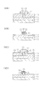
図3A〜3Dは、他の変形例を示す。埋め込み絶縁層を酸化シリコン層ではなく、窒化シリコン層又は酸窒化シリコン層12xで形成したSOI基板を用いる。この場合、窒化シリコン層を形成しなくても埋め込み絶縁層12x自身がエッチストッパとして機能する。図3A〜3Cは、図2A〜2Cに対応する工程を示す。
3A to 3D show another modification. An SOI substrate in which the buried insulating layer is formed of a silicon nitride layer or a
フィン型シリコン領域13の平面形状を図3Dに示すように、ソース/ドレインのコンタクト領域で幅広にする。この幅広のコンタクト領域においてシリサイド層24を形成し、その上に引き出し電極を形成する。フィン型構造の幅が狭くなると、ソース/ドレイン領域のコンタクト領域において両側面にシリサイド層を形成した時、シリサイド層が相互に接してしまう場合が生じ得る。シリサイドは、金属に対して十分シリサイド反応が進んだ状態が低抵抗状態である。両側面からのシリサイド層が接してしまうと、シリコンが不足する場合が生じ得る。すると、シリサイド層の低抵抗化を十分行なうことができなくなる。コンタクト領域を幅広にすることにより、このような可能性を排除し、十分低抵抗のシリサイド層を形成することができる。
As shown in FIG. 3D, the planar shape of the fin-
図4A〜4Dは、さらの他の変形例を示す。図4A、4Bは、サイドウォール絶縁層21を形成した状態を示す断面図である。図4Aがゲート電極16を含む位置の断面図、図4Bがゲート電極から外れたソース/ドレイン領域での断面図である。この状態において、ソース/ドレイン領域のシリコン層13は上面が露出し、ゲート電極16もその平坦部の上面は露出している。斜めイオン注入などにより、ソース/ドレイン領域18を形成する。
4A-4D show yet another variation. 4A and 4B are cross-sectional views showing a state where the
図4C、4Dは、この状態でシリサイド反応を行なった構成を示す。露出しているシリコン層にシリサイド層25が形成される。
4C and 4D show a configuration in which the silicide reaction is performed in this state. A
その後、層間絶縁膜堆積、コンタクトホール形成、シリサイド反応を行なうことにより、サイドウォール絶縁層21が存在していた部分にもシリサイド層が形成される。フィン型シリコン領域の上面には、2回シリサイド処理が行なわれることになる。
Thereafter, by performing interlayer insulating film deposition, contact hole formation, and silicide reaction, a silicide layer is also formed in the portion where the
以上実施例に沿って本発明を説明したが、本発明はこれらに制限されるものではない。例えば種々の変更、改良、組み合わせが可能なことは当業者に自明であろう。 Although the present invention has been described with reference to the embodiments, the present invention is not limited thereto. It will be apparent to those skilled in the art that various modifications, improvements, combinations, and the like can be made.
11 (Si)支持基板
12 埋め込み酸化シリコン層(BOX層)
12x 窒化シリコン(酸化窒化シリコン)層
13 シリコン層(フィン型半導体領域)
14 窒化シリコン層
15、17 CVD酸化シリコン層
16 ポリシリコン層
18 ソース/ドレイン領域
RM レジストマスク
CL キャップ層
21 サイドウォール酸化膜(絶縁層)
22 層間絶縁層
23 金属(Co,Ni)層
24 シリサイド層
CH コンタクトホール
11 (Si)
12x silicon nitride (silicon oxynitride)
14
22
Claims (9)
前記支持基板上に形成され、支持基板表面に対してほぼ垂直な一対の側面および前記両側面を接続する上面を有し、第1導電型を有するフィン型半導体領域と、
前記フィン型半導体領域の中間部を横断して形成され、ゲート絶縁膜とその上に形成された導電性ゲート電極とを含む絶縁ゲート電極構造と、
前記導電性ゲート電極両側の前記フィン型半導体領域に第2導電型不純物を添加して形成された、第2導電型を有するソース/ドレイン領域と、
前記導電性ゲート電極の側壁上に形成された第1サイドウォール絶縁膜と、前記フィン型半導体領域の側壁上に形成され、前記ソース/ドレイン領域上において、前記フィン型半導体領域の側面の上端から下端に達する開口を有する第2サイドウォール絶縁膜と、を含むサイドウォール絶縁膜と、
前記サイドウォール絶縁膜の開口内に露出された前記ソース/ドレイン領域の表面に形成されたシリサイド層と、
前記シリサイド層にコンタクトするソース/ドレイン電極と、
前記フィン型半導体領域、前記絶縁ゲート電極構造を埋め込み、前記サイドウォール絶縁膜の開口を露出するコンタクトホールを有する層間絶縁膜と、
を有し、前記シリサイド層は前記コンタクトホール内に形成されている半導体装置。 A support substrate having an insulating surface;
A fin-type semiconductor region having a first conductivity type, formed on the support substrate, having a pair of side surfaces substantially perpendicular to the support substrate surface and an upper surface connecting the both side surfaces;
The formed across the middle portion of the fin-type semiconductor region, a gate insulating film and including insulation gate electrode structure and a formed conductive gate electrode thereon,
A source / drain region having a second conductivity type formed by adding a second conductivity type impurity to the fin-type semiconductor region on both sides of the conductive gate electrode;
A first sidewall insulating film formed on the sidewall of the conductive gate electrode and a sidewall of the fin-type semiconductor region, and from the upper end of the side surface of the fin-type semiconductor region on the source / drain region A side wall insulating film including a second side wall insulating film having an opening reaching the lower end;
A silicide layer formed on the surface of the source / drain region exposed in the opening of the sidewall insulating film;
Source / drain electrodes in contact with the silicide layer;
An interlayer insulating film having a contact hole that embeds the fin-type semiconductor region and the insulating gate electrode structure and exposes an opening of the sidewall insulating film;
And the silicide layer is formed in the contact hole .
前記ゲート絶縁膜は前記フィン型半導体層の側面上に形成され、前記シリサイド層は前記フィン型半導体領域の側面上に形成されている請求項1記載の半導体装置。 And an insulating protective film formed on the upper surface of the fin-type semiconductor region,
2. The semiconductor device according to claim 1, wherein the gate insulating film is formed on a side surface of the fin-type semiconductor layer, and the silicide layer is formed on a side surface of the fin-type semiconductor region.
(b)前記フィン型半導体領域の中間部を横断し、ゲート絶縁膜とその上の導電性ゲート電極とを含む絶縁ゲート電極構造を形成する工程と、
(c)前記フィン型半導体領域および前記絶縁ゲート電極構造の側面上にサイドウォール絶縁膜を形成する工程と、
(d)前記絶縁ゲート電極構造両側の前記フィン型半導体領域にソース/ドレイン領域を形成する工程と、
(e)前記サイドウォール絶縁膜を覆って、層間絶縁膜を堆積する工程と、
(f)前記層間絶縁膜を貫通して前記ソース/ドレイン領域に達するコンタクトホールを開口すると共に、前記コンタクトホール内の前記サイドウォール絶縁膜を除去し、前記ソース/ドレイン領域を露出する工程と、
(g)前記コンタクトホール内に露出した前記ソース/ドレイン領域にシリサイド層を形成する工程と、
を含む半導体装置の製造方法。 (A) A step of patterning a semiconductor layer of an SOI substrate to form a fin-type semiconductor region having a pair of side surfaces substantially perpendicular to the support substrate surface and an upper surface connecting the both side surfaces on the support substrate having an insulating surface. When,
(B) across the intermediate portion of the fin-type semiconductor region, a step of a conductive gate electrode thereon a gate insulating film to form a including insulation gate electrode structure,
(C) forming a sidewall insulating film on a side surface of the fin-type semiconductor region and the insulated gate electrode structure;
(D) forming source / drain regions in the fin-type semiconductor regions on both sides of the insulated gate electrode structure;
(E) depositing an interlayer insulating film so as to cover the sidewall insulating film;
(F) opening a contact hole that reaches the source / drain region through the interlayer insulating film, removing the sidewall insulating film in the contact hole, and exposing the source / drain region;
(G) forming a silicide layer in the source / drain region exposed in the contact hole;
A method of manufacturing a semiconductor device including:
Priority Applications (3)
| Application Number | Priority Date | Filing Date | Title |
|---|---|---|---|
| JP2005008855A JP4527552B2 (en) | 2005-01-17 | 2005-01-17 | Semiconductor device and manufacturing method thereof |
| US11/123,145 US7282766B2 (en) | 2005-01-17 | 2005-05-06 | Fin-type semiconductor device with low contact resistance |
| US11/896,826 US7396710B2 (en) | 2005-01-17 | 2007-09-06 | Fin-type semiconductor device with low contact resistance and its manufacture method |
Applications Claiming Priority (1)
| Application Number | Priority Date | Filing Date | Title |
|---|---|---|---|
| JP2005008855A JP4527552B2 (en) | 2005-01-17 | 2005-01-17 | Semiconductor device and manufacturing method thereof |
Publications (2)
| Publication Number | Publication Date |
|---|---|
| JP2006196822A JP2006196822A (en) | 2006-07-27 |
| JP4527552B2 true JP4527552B2 (en) | 2010-08-18 |
Family
ID=36802631
Family Applications (1)
| Application Number | Title | Priority Date | Filing Date |
|---|---|---|---|
| JP2005008855A Expired - Fee Related JP4527552B2 (en) | 2005-01-17 | 2005-01-17 | Semiconductor device and manufacturing method thereof |
Country Status (1)
| Country | Link |
|---|---|
| JP (1) | JP4527552B2 (en) |
Families Citing this family (3)
| Publication number | Priority date | Publication date | Assignee | Title |
|---|---|---|---|---|
| WO2009144874A1 (en) * | 2008-05-29 | 2009-12-03 | Panasonic Corporation | Finfet with impurity blocking portion on an upper surface of fin |
| JP5305969B2 (en) * | 2009-02-17 | 2013-10-02 | 株式会社東芝 | Semiconductor device |
| US9887192B2 (en) * | 2016-06-30 | 2018-02-06 | Globalfoundries Inc. | Interconnects for vertical-transport field-effect transistors |
Family Cites Families (2)
| Publication number | Priority date | Publication date | Assignee | Title |
|---|---|---|---|---|
| JP2002118255A (en) * | 2000-07-31 | 2002-04-19 | Toshiba Corp | Semiconductor device and manufacturing method thereof |
| US7358121B2 (en) * | 2002-08-23 | 2008-04-15 | Intel Corporation | Tri-gate devices and methods of fabrication |
-
2005
- 2005-01-17 JP JP2005008855A patent/JP4527552B2/en not_active Expired - Fee Related
Also Published As
| Publication number | Publication date |
|---|---|
| JP2006196822A (en) | 2006-07-27 |
Similar Documents
| Publication | Publication Date | Title |
|---|---|---|
| US7282766B2 (en) | Fin-type semiconductor device with low contact resistance | |
| US9887274B2 (en) | FinFETs and methods for forming the same | |
| CN106098775B (en) | Semiconductor device with a plurality of transistors | |
| US7648883B2 (en) | Phosphorous doping methods of manufacturing field effect transistors having multiple stacked channels | |
| US7229884B2 (en) | Phosphorous doping methods of manufacturing field effect transistors having multiple stacked channels | |
| US20040132236A1 (en) | Mos transistor | |
| CN103050407B (en) | Embedded Transistor | |
| JP2006294995A (en) | Field effect transistor and manufacturing method thereof | |
| TWI807067B (en) | Semiconductor structure and method for manufacturing the same and finfet device and gate structure | |
| WO2006132172A1 (en) | Fin type field effect transistor, semiconductor device and production method thereof | |
| TW202207461A (en) | Transistor and manufacturing method thereof | |
| TWI854640B (en) | Nanostructure field-effect transistor and manufacturing method thereof | |
| TWI860699B (en) | Semiconductor device and method of forming same | |
| JP5224769B2 (en) | CMOS structure including a three-dimensional active region | |
| TW202133271A (en) | Semiconductor device | |
| US8378395B2 (en) | Methods of fabricating field effect transistors having protruded active regions | |
| JP4950064B2 (en) | Saddle type MOS element | |
| TW202207468A (en) | Semiconductor device and method | |
| JP2006196821A (en) | Semiconductor device and manufacturing method thereof | |
| JP2006054423A (en) | Semiconductor device and manufacturing method thereof | |
| CN115881771A (en) | Transistor, semiconductor device and forming method thereof | |
| JP4527552B2 (en) | Semiconductor device and manufacturing method thereof | |
| JP2013235880A (en) | Semiconductor device and method of manufacturing the same | |
| CN113206089A (en) | Semiconductor devices and methods | |
| CN100550424C (en) | Semiconductor device and method for manufacturing the same |
Legal Events
| Date | Code | Title | Description |
|---|---|---|---|
| A711 | Notification of change in applicant |
Free format text: JAPANESE INTERMEDIATE CODE: A712 Effective date: 20080729 |
|
| A977 | Report on retrieval |
Free format text: JAPANESE INTERMEDIATE CODE: A971007 Effective date: 20090126 |
|
| A131 | Notification of reasons for refusal |
Free format text: JAPANESE INTERMEDIATE CODE: A131 Effective date: 20091020 |
|
| A521 | Request for written amendment filed |
Free format text: JAPANESE INTERMEDIATE CODE: A523 Effective date: 20091221 |
|
| TRDD | Decision of grant or rejection written | ||
| A01 | Written decision to grant a patent or to grant a registration (utility model) |
Free format text: JAPANESE INTERMEDIATE CODE: A01 Effective date: 20100601 |
|
| A01 | Written decision to grant a patent or to grant a registration (utility model) |
Free format text: JAPANESE INTERMEDIATE CODE: A01 |
|
| A61 | First payment of annual fees (during grant procedure) |
Free format text: JAPANESE INTERMEDIATE CODE: A61 Effective date: 20100603 |
|
| FPAY | Renewal fee payment (event date is renewal date of database) |
Free format text: PAYMENT UNTIL: 20130611 Year of fee payment: 3 |
|
| R150 | Certificate of patent or registration of utility model |
Free format text: JAPANESE INTERMEDIATE CODE: R150 |
|
| LAPS | Cancellation because of no payment of annual fees |