JP4523005B2 - Coplanar waveguide line - Google Patents
Coplanar waveguide line Download PDFInfo
- Publication number
- JP4523005B2 JP4523005B2 JP2006537401A JP2006537401A JP4523005B2 JP 4523005 B2 JP4523005 B2 JP 4523005B2 JP 2006537401 A JP2006537401 A JP 2006537401A JP 2006537401 A JP2006537401 A JP 2006537401A JP 4523005 B2 JP4523005 B2 JP 4523005B2
- Authority
- JP
- Japan
- Prior art keywords
- coplanar
- substrate
- coplanar waveguide
- electrode
- extending
- Prior art date
- Legal status (The legal status is an assumption and is not a legal conclusion. Google has not performed a legal analysis and makes no representation as to the accuracy of the status listed.)
- Expired - Fee Related
Links
Images


Classifications
-
- G—PHYSICS
- G02—OPTICS
- G02F—OPTICAL DEVICES OR ARRANGEMENTS FOR THE CONTROL OF LIGHT BY MODIFICATION OF THE OPTICAL PROPERTIES OF THE MEDIA OF THE ELEMENTS INVOLVED THEREIN; NON-LINEAR OPTICS; FREQUENCY-CHANGING OF LIGHT; OPTICAL LOGIC ELEMENTS; OPTICAL ANALOGUE/DIGITAL CONVERTERS
- G02F1/00—Devices or arrangements for the control of the intensity, colour, phase, polarisation or direction of light arriving from an independent light source, e.g. switching, gating or modulating; Non-linear optics
- G02F1/01—Devices or arrangements for the control of the intensity, colour, phase, polarisation or direction of light arriving from an independent light source, e.g. switching, gating or modulating; Non-linear optics for the control of the intensity, phase, polarisation or colour
- G02F1/21—Devices or arrangements for the control of the intensity, colour, phase, polarisation or direction of light arriving from an independent light source, e.g. switching, gating or modulating; Non-linear optics for the control of the intensity, phase, polarisation or colour by interference
- G02F1/225—Devices or arrangements for the control of the intensity, colour, phase, polarisation or direction of light arriving from an independent light source, e.g. switching, gating or modulating; Non-linear optics for the control of the intensity, phase, polarisation or colour by interference in an optical waveguide structure
- G02F1/2257—Devices or arrangements for the control of the intensity, colour, phase, polarisation or direction of light arriving from an independent light source, e.g. switching, gating or modulating; Non-linear optics for the control of the intensity, phase, polarisation or colour by interference in an optical waveguide structure the optical waveguides being made of semiconducting material
-
- G—PHYSICS
- G02—OPTICS
- G02F—OPTICAL DEVICES OR ARRANGEMENTS FOR THE CONTROL OF LIGHT BY MODIFICATION OF THE OPTICAL PROPERTIES OF THE MEDIA OF THE ELEMENTS INVOLVED THEREIN; NON-LINEAR OPTICS; FREQUENCY-CHANGING OF LIGHT; OPTICAL LOGIC ELEMENTS; OPTICAL ANALOGUE/DIGITAL CONVERTERS
- G02F1/00—Devices or arrangements for the control of the intensity, colour, phase, polarisation or direction of light arriving from an independent light source, e.g. switching, gating or modulating; Non-linear optics
- G02F1/01—Devices or arrangements for the control of the intensity, colour, phase, polarisation or direction of light arriving from an independent light source, e.g. switching, gating or modulating; Non-linear optics for the control of the intensity, phase, polarisation or colour
- G02F1/21—Devices or arrangements for the control of the intensity, colour, phase, polarisation or direction of light arriving from an independent light source, e.g. switching, gating or modulating; Non-linear optics for the control of the intensity, phase, polarisation or colour by interference
- G02F1/225—Devices or arrangements for the control of the intensity, colour, phase, polarisation or direction of light arriving from an independent light source, e.g. switching, gating or modulating; Non-linear optics for the control of the intensity, phase, polarisation or colour by interference in an optical waveguide structure
- G02F1/2255—Devices or arrangements for the control of the intensity, colour, phase, polarisation or direction of light arriving from an independent light source, e.g. switching, gating or modulating; Non-linear optics for the control of the intensity, phase, polarisation or colour by interference in an optical waveguide structure controlled by a high-frequency electromagnetic component in an electric waveguide structure
Landscapes
- Physics & Mathematics (AREA)
- Nonlinear Science (AREA)
- General Physics & Mathematics (AREA)
- Optics & Photonics (AREA)
- Electromagnetism (AREA)
- Optical Modulation, Optical Deflection, Nonlinear Optics, Optical Demodulation, Optical Logic Elements (AREA)
- Waveguide Aerials (AREA)
- Diaphragms For Electromechanical Transducers (AREA)
- Optical Integrated Circuits (AREA)
- Semiconductor Lasers (AREA)
Abstract
Description
本発明は、本発明は共平面導波管線路に関するものである。本発明はまた、そのような共平面導波管線路を備えたマッハツェンダ(Mach−Zehnder)変調器に関するものである。 The present invention relates to a coplanar waveguide line. The invention also relates to a Mach-Zehnder modulator comprising such a coplanar waveguide line.
マッハツェンダ変調器を高額信号の減衰器として使用することは周知である。非特許文献(アイトリプルイー・トランザクションズ・オン・マイクロウェーブ・セオリー・アンド・テクニークス第47巻第7号1999年7月号)はそのような装置の動作の背景的検討を提供している。 It is well known to use a Mach-Zehnder modulator as an attenuator for expensive signals. Non-patent literature (I Triple E Transactions on Microwave Theory and Technology, Vol. 47, No. 7, July 1999) provides a background study of the operation of such devices. .
そのような変調器の帯域幅は装置を通過する光波とマイクロ波の間の伝搬速度の不整合に反比例する。典型的には、ガリウムヒ素のような基板を用いるときに、マイクロ波の速度を遅くして光波の速度に整合させて装置の帯域幅を広げようとすることが試みられる。ニオブ酸リチウム基板では逆のことが行われる。 The bandwidth of such a modulator is inversely proportional to the propagation velocity mismatch between the light wave and microwave passing through the device. Typically, when using a substrate such as gallium arsenide, attempts are made to slow the microwave speed to match the speed of the light wave to increase the bandwidth of the device. The reverse is done for lithium niobate substrates.
既知の共平面導波管線路は中央電極ストリップと、この中央電極ストリップのそれぞれの側の第1および第2の電極ストリップとを備える。使用時は、第1および第2の電極ストリップは中央電極ストリップとは反対の同じ極性を持つ。中央電極ストリップの両側からT−レールが第1および第2の光導波路の近くまで延びており、遅波効果を与える。 A known coplanar waveguide line comprises a central electrode strip and first and second electrode strips on each side of the central electrode strip. In use, the first and second electrode strips have the same polarity opposite the central electrode strip. T-rails extend from both sides of the central electrode strip to near the first and second optical waveguides to provide a slow wave effect.
そのような共平面導波管線路は一般に未ドープ・エピタキシャル層とともに用いられる。これの利点はマイクロ波の損失が非常に低損失であることにある。しかしながら、光波とマイクロ波の間の重なりにより駆動電圧が高くなければならない。 Such coplanar waveguide lines are generally used with undoped epitaxial layers. The advantage of this is that the microwave loss is very low. However, the drive voltage must be high due to the overlap between light waves and microwaves.
非対称共平面ストリップ線路も遅波構造として用いられる。非対称共平面ストリップは中央電極ストリップを欠いている。光導波路は第1および第2の平行電極ストリップの間に配置され、これらの平行電極ストリップは使用時に反対の極性を有する。T−レールがこれらストリップから導波路に延びている。 Asymmetric coplanar striplines are also used as slow wave structures. The asymmetric coplanar strip lacks the central electrode strip. The optical waveguide is disposed between the first and second parallel electrode strips, and these parallel electrode strips have opposite polarities in use. T-rails extend from these strips into the waveguide.
共平面導波管線路を用いた場合と異なり、非対称共平面ストリップは、導波路間に延びているn+ 導電層を含む基板上で用いられる。導電層を使用すると駆動電圧は低減されるが、マイクロ波損失は増加する。 Unlike using coplanar waveguide lines, asymmetric coplanar strips are used on a substrate that includes an n + conductive layer extending between the waveguides. Using a conductive layer reduces the drive voltage but increases the microwave loss.
当技術においては、n+ 導電層を共平面導波路のエピタキシャル層に含めないことが知られている。これにより光波とマイクロ波の重なりが改善される(それにより駆動電圧が低下する)ものの、この結果、キャパシタンスが超過し、真のプッシュ・プル動作が不可能になる。 It is known in the art that the n + conductive layer is not included in the epitaxial layer of the coplanar waveguide. This improves the overlap between the light wave and the microwave (thus lowering the drive voltage), but as a result, the capacitance is exceeded and true push-pull operation is not possible.
従って、一態様において、本発明は、共平面導波管線路であって、
基板と、
前記基板上の中央電極ストリップと、
前記中央電極ストリップの反対側に配置され、かつそれらに平行に延びている、第1および第2の電極ストリップと、
前記基板上の第1および第2の光導波路であって、前記第1および第2の電極ストリップのあいだに配置され、かつそれらに平行に延びている前記光導波路を備え、
前記中央電極は前記第1の光導波路の近傍に延びている少なくとも1つのT−レールを備え、
前記第1の電極は前記第2の光導波路の近傍に延びている少なくとも1つのT−レールを備え、
前記基板は前記光導波路間に延びているn+ 導電層を備え、
前記共平面導波管線路は、さらに、第1および第2の電極ストリップの間の電気接続を備える共平面導波管線路を提供する。
Thus, in one aspect, the present invention is a coplanar waveguide line,
A substrate,
A central electrode strip on the substrate;
First and second electrode strips disposed opposite and extending parallel to the central electrode strip;
First and second optical waveguides on the substrate, wherein the optical waveguides are disposed between and extend parallel to the first and second electrode strips;
The central electrode comprises at least one T-rail extending in the vicinity of the first optical waveguide;
The first electrode comprises at least one T-rail extending in the vicinity of the second optical waveguide;
The substrate comprises an n + conductive layer extending between the optical waveguides;
The coplanar waveguide line further provides a coplanar waveguide line comprising an electrical connection between the first and second electrode strips.
本発明による共平面導波路の利点は、既知の共平面導波路の低マイクロ波損失を非対称共平面ストリップとn+ 導電層との組合せの低駆動電圧に組み合わせたことにある。さらに、T−レールは中央電極の一方の側にのみ追加されるので、キャパシタンスを半分にすることが可能であり、伝送線路の設計の自由度がより大きくなり、かつ伝送線路をMMIC伝送線路設計に適用することが可能になる。 The advantage of the coplanar waveguide according to the invention is that it combines the low microwave loss of known coplanar waveguides with the low drive voltage of the combination of an asymmetric coplanar strip and an n + conductive layer. Furthermore, since the T-rail is added only on one side of the central electrode, the capacitance can be halved, the degree of freedom in designing the transmission line is increased, and the transmission line is designed for MMIC transmission line design. It becomes possible to apply to.
さらに、共平面導波路と非対称共平面ストリップの間またはその逆の伝送に不連続性が存在することが知られている。これは、往々にして、装置の設計の際に、共平面導波路または非対称共平面ストリップの選択を限定することがある。本発明の共平面導波管線路と既知の導波路構造との間にはそのような不連続性は存在しない。 It is further known that discontinuities exist in the transmission between coplanar waveguides and asymmetric coplanar strips or vice versa. This often limits the choice of coplanar waveguides or asymmetric coplanar strips during device design. There is no such discontinuity between the coplanar waveguide line of the present invention and the known waveguide structure.
好ましくは、第1および第2の電極ストリップの間の電気的接続はエアーブリッジ(airbridge)である。この電気的接続は第1および第2の電極ストリップ間でワイヤボンディングすることが可能である。第1および第2の電極間の電気的接続は基板の裏面を通すことが可能である。そのような接続手段は、第1及び第2の電極ストリップを接続する、信頼性に富む比較的簡単な手段を提供する。 Preferably, the electrical connection between the first and second electrode strips is an air bridge. This electrical connection can be wire bonded between the first and second electrode strips. The electrical connection between the first and second electrodes can pass through the back surface of the substrate. Such a connection means provides a reliable and relatively simple means of connecting the first and second electrode strips.
好ましくは、共平面導波管線路は第1および第2の電極ストリップ間の複数の電気的接続を備え、これらの電気的接続は等間隔であることが好ましい。そのような多接続により、共平面導波路のキャパシタンスの負荷が不平衡であってもその影響が最小限になる。 Preferably, the coplanar waveguide line comprises a plurality of electrical connections between the first and second electrode strips, and these electrical connections are preferably equally spaced. Such multiple connections minimize the effects of unbalanced coplanar waveguide capacitance loading.
好ましくは、中央電極ストリップと第1の電極ストリップの少なくとも一方は複数のT−レール、好ましくは等間隔に設けたものを備える。 Preferably, at least one of the central electrode strip and the first electrode strip comprises a plurality of T-rails, preferably at equal intervals.
T−レールは対応する電極ストリップにブリッジで接続された導体パッドを備える。好ましくは、導体パッドは光導波路に当接する。これにより、光波とマイクロ波の良好な重なりが保証される。 The T-rail comprises conductor pads connected by bridges to corresponding electrode strips. Preferably, the conductor pad contacts the optical waveguide. This ensures a good overlap between the light wave and the microwave.
基板は第1の分離溝を備えることが可能であり、この分離溝は第1の電極ストリップと光導波路の間のn+ 導電層を通って延びている。基板は第2の分離溝を備えることが可能であり、この分離溝は中央電極ストリップと光導波路の間のn+ 導電層を通って延びている。基板は第3の第2の分離溝を備えることが可能であり、この分離溝は中央電極ストリップと第2の電極ストリップの間のn+ 導電層を通って延びている。 The substrate can comprise a first isolation groove, which extends through the n + conductive layer between the first electrode strip and the optical waveguide. The substrate can comprise a second isolation groove, which extends through the n + conductive layer between the central electrode strip and the optical waveguide. The substrate can comprise a third second isolation groove, which extends through the n + conductive layer between the central electrode strip and the second electrode strip.
本発明のさらなる態様において、本発明の共平面導波路を含むマッハツェンダ変調器が提供される。 In a further aspect of the present invention, there is provided a Mach-Zehnder modulator comprising the coplanar waveguide of the present invention.
以下に、添付図面を参照して本発明を例示的にのみ、そして如何なる意味においても非限定的に説明する。 The invention will now be described by way of example only and in a non-limiting manner with reference to the accompanying drawings.
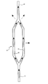
図1aおよび図1bに概略形状で示されているのはマッハツェンダ変調器(1)である。マッハツェンダ変調器(1)は入力および出力光導波路(2、3)と、それらの間に延びている2つの光路(4、5)とを備えている。2つの光路(4、5)は実質的に等しい長さである。 Shown in schematic form in FIGS. 1a and 1b is a Mach-Zehnder modulator (1). The Mach-Zehnder modulator (1) comprises input and output optical waveguides (2, 3) and two optical paths (4, 5) extending between them. The two optical paths (4, 5) are substantially equal in length.
使用時、コヒーレント光線をマッハツェンダ変調器(1)に導入する。この光線はほぼ等しい半分同士に分割され、2つの別個の経路(4、5)を通って出力導波路(3)に至る。光線は出力導波路(3)において再結合してから装置を出る。これら2つの経路が同じ長さであると仮定すると、2つの光線が再結合すると、それらは同位相であり、得られた出力光は入力光と同じ強度である。 In use, a coherent beam is introduced into the Mach-Zehnder modulator (1). This ray is split into approximately equal halves and through two separate paths (4, 5) to the output waveguide (3). The rays recombine in the output waveguide (3) before exiting the device. Assuming that these two paths are the same length, when the two rays recombine, they are in phase and the resulting output light is the same intensity as the input light.
マッハツェンダ変調器(1)のアーム(4、5)の一方に(図1bに示すように)位相シフトを導入すると、2つの光線が再結合すると、それらは少し位相がずれる。この結果、出力光の強度が図示のように減少する。 If a phase shift is introduced into one of the arms (4, 5) of the Mach-Zehnder modulator (1) (as shown in FIG. 1b), when the two rays recombine, they are slightly out of phase. As a result, the intensity of the output light decreases as shown.
マッハツェンダ変調器のアーム(4、5)に位相シフトを導入する慣用方法が概略の形で図2に示されている。マッハツェンダ変調器(1)のアーム(4、5)のそれぞれのごく近傍に導電性電極ストリップ(6、7)がある。マイクロ波発生器(8)を電極ストリップ(6、7)に接続し、生じた電磁場がアーム(4、5)を通過する光と相互作用して光の位相を変化させる。図示のように、電極ストリップ(6、7)をプッシュ/プル構成で接続して2つの電極ストリップ(6、7)に印加される電圧の位相が180度ずれるようにするのが普通である。これにより、電磁波の位相変化効果が最大となる。 A conventional method for introducing a phase shift into the arms (4, 5) of a Mach-Zehnder modulator is shown in schematic form in FIG. There are conductive electrode strips (6, 7) in the immediate vicinity of each arm (4, 5) of the Mach-Zehnder modulator (1). A microwave generator (8) is connected to the electrode strips (6, 7) and the resulting electromagnetic field interacts with the light passing through the arms (4, 5) to change the phase of the light. As shown, it is common to connect the electrode strips (6, 7) in a push / pull configuration so that the voltage applied to the two electrode strips (6, 7) is 180 degrees out of phase. This maximizes the phase change effect of the electromagnetic wave.
マッハツェンダ変調器(1)の帯域は電極ストリップ(6、7)に沿うマイクロ波とマッハツェンダ変調器(1)のアーム(4、5)に沿う光波の間の伝搬速度の不整合により限定される。この帯域は下式により与えられる。 The band of the Mach-Zehnder modulator (1) is limited by the mismatch in propagation speed between the microwaves along the electrode strips (6, 7) and the light waves along the arms (4, 5) of the Mach-Zehnder modulator (1). This band is given by:

GaAsに対して、nopt≒2.64、nmw≒3.34、そしてLT=0.01メートルであり、≒19GHzの3dB帯域が得られる。 For GaAs, n opt ≈2.64, n mw ≈3.34, and L T = 0.01 meter, resulting in a 3 dB band of ≈19 GHz.
この問題を克服するために、そしてマッハツェンダ変調器(1)の帯域を広げるために、典型的には、装置を通るマイクロ波の伝搬速度を低減することが試みられる。本質的に、既知の遅波導波路構造の2つの形態−共平面導波管線路(9)および非対称共平面ストリップ線路(10)がある。 To overcome this problem and to increase the bandwidth of the Mach-Zehnder modulator (1), it is typically attempted to reduce the propagation speed of microwaves through the device. In essence, there are two forms of known slow wave waveguide structures—coplanar waveguide lines (9) and asymmetric coplanar striplines (10).
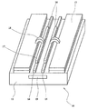
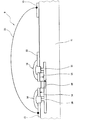
図3に斜視図が示されているのは既知の非対称共平面ストリップ(ACPS)(10)である。ACPS(10)は基板(11)を備え、基板(11)上に第1および第2のストリップ電極(12、13)が配置されている。ストリップ電極(12、13)の間に配置され、かつそれらに平行に延びているのは第1および第2の光導波路(14、15)である。T−レール(16)がストリップ電極(12、13)から光導波路(14、15)の近傍に延びている。各T−レール(16)は光導波路(14、15)と当接する導電パッド(17)と、導電パッド(17)と対応するストリップ電極(12、13)の間に延びているエアーブリッジ(18)とを備えている。 Shown in FIG. 3 is a known asymmetric coplanar strip (ACPS) (10). The ACPS (10) includes a substrate (11), and first and second strip electrodes (12, 13) are disposed on the substrate (11). Disposed between and extending parallel to the strip electrodes (12, 13) are first and second optical waveguides (14, 15). A T-rail (16) extends from the strip electrodes (12, 13) in the vicinity of the optical waveguides (14, 15). Each T-rail (16) has a conductive pad (17) in contact with the optical waveguide (14, 15) and an air bridge (18) extending between the conductive pad (17) and the corresponding strip electrode (12, 13). ).
基板(11)内にはn+ 導電層がある。図4から分かるように、n+ 導電層(19)は光導波路(14、15)の間に延びており、それらの間の電気的接続を提供している。分離溝(20、21)が図示のように光導波路の両側でn+ 導電層(19)を通って延びている。n+ 導電層(19)は電極ストリップ(12、13)の下方に延びている。 Within the substrate (11) is an n + conductive layer. As can be seen from FIG. 4, an n + conductive layer (19) extends between the optical waveguides (14, 15) and provides an electrical connection therebetween. Separation grooves (20, 21) extend through the n + conductive layer (19) on both sides of the optical waveguide as shown. The n + conductive layer (19) extends below the electrode strips (12, 13).
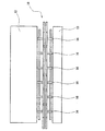
図5は図3および図4の非対称共平面ストリップ(10)を平面図で示す。両電極ストリップ(12、13)は、関連する光導波路(14、15)まで延びている複数のT−レールを(16)を備えている。T−レール(16)は等間隔である。T−レール(16)はマイクロ波を遅らせ、帯域を増加させる。 FIG. 5 shows the asymmetric coplanar strip (10) of FIGS. 3 and 4 in plan view. Both electrode strips (12, 13) are provided with a plurality of T-rails (16) extending to the associated optical waveguides (14, 15). The T-rails (16) are equally spaced. The T-rail (16) delays the microwave and increases the bandwidth.
n+ 導電層(19)の存在するため、非対称共平面ストリップ(10)は低駆動電圧しか必要としない。しかしながら、それらはマイクロ波損失特性が悪い傾向がある。 Due to the presence of the n + conductive layer (19), the asymmetric coplanar strip (10) requires only a low drive voltage. However, they tend to have poor microwave loss characteristics.
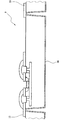
図6に断面図で示したのは、既知の共平面導波管線路(9)である。共平面導波管線路(9)はGaAs基板(11)を備える。基板(11)上には、両側に第1および第2の電極ストリップ(12、13)を有する中央電極ストリップ(22)が配置されている。第1および第2の光導波路は第1の電極ストリップ(12)と中央電極ストリップ(22)の間、および中央電極ストリップ(22)と第2の電極ストリップ(13)の間にそれぞれ配置されている。T−レール(16)は中央電極ストリップ(22)の両側から延びており、また第1および第2の電極ストリップ(12、13)の両方から延びている。第2の電極ストリップ(13)および中央電極ストリップ(22)からのT−レール(16)は図示のように光導波路(14、15)に当接する。GaAs基板(11)はn+ 導電層を含まない。 A cross-sectional view shown in FIG. 6 is a known coplanar waveguide line (9). The coplanar waveguide line (9) comprises a GaAs substrate (11). A central electrode strip (22) having first and second electrode strips (12, 13) on both sides is arranged on the substrate (11). The first and second optical waveguides are disposed between the first electrode strip (12) and the central electrode strip (22) and between the central electrode strip (22) and the second electrode strip (13), respectively. Yes. The T-rail (16) extends from both sides of the central electrode strip (22) and extends from both the first and second electrode strips (12, 13). The T-rails (16) from the second electrode strip (13) and the central electrode strip (22) abut the optical waveguides (14, 15) as shown. The GaAs substrate (11) does not include an n + conductive layer.
n+ 導電層が存在しない種、共平面導波管線路(9)はマイクロ波損失が非常に低い。しかしながら、駆動電圧は光波とマイクロ波の重なりが悪いため、かなり高くなければならない。 The seed without the n + conductive layer, the coplanar waveguide line (9), has a very low microwave loss. However, the drive voltage must be quite high because the overlap between the light wave and the microwave is poor.
共平面導波管線路(9)は図7に平面図で示すが、図7はT−レール(16)の反復的性質を示している。 The coplanar waveguide line (9) is shown in plan view in FIG. 7, which shows the repetitive nature of the T-rail (16).
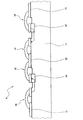
図8に示したのは本発明による共平面導波管線路(9)の断面図である。共平面導波管線路(9)はn+ 導電層(19)を埋設したGaAs基板(11)を備える。基板(11)上に配置されているのは中央電極ストリップ(22)と、中央電極ストリップ(22)のそれぞれの側にあり、かつそれに向かって延びている第1および第2の電極ストリップ(12、13)である。2つの平行な光導波路(14、15)が第1の電極ストリップ(12)と中央電極ストリップ(22)の間にそれらに平行に延びている。T−レール(16)が第1の電極ストリップ(12)と中央電極ストリップ(22)から図示のように光導波路(14、15)に延びている。n+ 導電層(19)がこれら2つの光導波路(14、15)の下方に延びている。第1および第2の分離溝(20、21)が、図示のように、光導波路(14、15)のそれぞれの側へn+ 導電層(19)を通って延びている。第1および第2の電極ストリップ(12、13)はワイヤボンディング(23)により相互に接続されている。さらなる(図示しない)実施形態では、第1および第2の電極ストリップ(12、13)はエアーブリッジにより接続されている。 FIG. 8 is a cross-sectional view of a coplanar waveguide line (9) according to the present invention. The coplanar waveguide line (9) includes a GaAs substrate (11) in which an n + conductive layer (19) is embedded. Disposed on the substrate (11) is a central electrode strip (22) and first and second electrode strips (12) on each side of the central electrode strip (22) and extending toward it. 13). Two parallel optical waveguides (14, 15) extend parallel to and between the first electrode strip (12) and the central electrode strip (22). A T-rail (16) extends from the first electrode strip (12) and the central electrode strip (22) to the light guide (14, 15) as shown. An n + conductive layer (19) extends below these two optical waveguides (14, 15). First and second isolation grooves (20, 21) extend through the n + conductive layer (19) to respective sides of the optical waveguide (14, 15) as shown. The first and second electrode strips (12, 13) are connected to each other by wire bonding (23). In a further (not shown) embodiment, the first and second electrode strips (12, 13) are connected by an air bridge.
本発明による共平面導波管線路(9)のさらなる実施形態を図9に示す。この実施形態の共平面導波管線路(9)は、図示のように、n+ 導電層(19)が中央電極ストリップ(22)の下方から第2の電極ストリップ(13)に延びている以外は前述の実施形態と同様である。しかしながら、前述の実施形態のように、n+ 導電層(19)のこの延長部は光導波路(14、15)の下のn+ 導電層(19)から第2の分離溝(21)により分離されている。第3の分離溝(24)が第2の電極ストリップ(13)と中央電極ストリップ(22)との間でn+ 導電層(19)を通って延びている。 A further embodiment of a coplanar waveguide line (9) according to the invention is shown in FIG. The coplanar waveguide line (9) of this embodiment has an n + conductive layer (19) extending from below the central electrode strip (22) to the second electrode strip (13) as shown in the figure. Is the same as in the previous embodiment. However, as in the embodiment described above separated by, n + conductive layer (19) This second isolation groove from n + conductive layer underneath (19) of the extension waveguide (14, 15) (21) of Has been. A third separation groove (24) extends through the n + conductive layer (19) between the second electrode strip (13) and the central electrode strip (22).
図10に示されているのは、図9の共平面導波管線路(9)の平面図である。この図は電極ストリップ(12、22)に沿うT−レールの反復性を示す。第1および第2の電極ストリップ(12、13)は複数のエアーブリッジ(25)により電気的に接続され、エアーブリッジ(25)は実質的に等間隔である。別の実施形態では、第1および第2の電極ストリップ(12、13)はワイヤボンディング(23)により電気的に接続されている。 Shown in FIG. 10 is a plan view of the coplanar waveguide line (9) of FIG. This figure shows the repeatability of the T-rail along the electrode strips (12, 22). The first and second electrode strips (12, 13) are electrically connected by a plurality of air bridges (25), and the air bridges (25) are substantially equally spaced. In another embodiment, the first and second electrode strips (12, 13) are electrically connected by wire bonding (23).
図11に示されているのは、本発明による共平面導波管線路(9)のさらなる実施形態である。この実施形態は第1および第2の電極ストリップ(12、13)が基板を通って延びている電気的接続(26)により接続されている事以外は図8に示す実施形態と同様である。 Shown in FIG. 11 is a further embodiment of a coplanar waveguide line (9) according to the invention. This embodiment is similar to the embodiment shown in FIG. 8 except that the first and second electrode strips (12, 13) are connected by an electrical connection (26) extending through the substrate.
図12および図13に示されているのは本発明による共平面導波管線路の性能に関するデータである。 12 and 13 show data relating to the performance of the coplanar waveguide line according to the present invention.
共平面導波管線路の測定されたSパラメータのS11およびS21の大きさを図12および図13にそれぞれ示す。図12および図13では、2つの曲線(plots)間の大きな差は接地ストラップが存在するか否かである。図13では、接地ストラップなしのCPWに対するS11スペクトルに、周波数が増加されたときに、強い共鳴が規則的に現れる。これらの共鳴は、図12に示すCPWに対するS21スペクトルにおけるリップルに相当する。これらの共鳴は第1および第2の電極ストリップの間をストラッピングすると消失した。接地ストラッピングを用いることでS21では30Ghzまでの滑らかな共鳴およびS11では低い反射が実現された。 The magnitudes of measured S-parameters S11 and S21 of the coplanar waveguide line are shown in FIGS. 12 and 13, respectively. In FIGS. 12 and 13, the major difference between the two curves is whether or not a ground strap exists. In FIG. 13, strong resonances regularly appear in the S11 spectrum for CPW without a ground strap when the frequency is increased. These resonances correspond to ripples in the S21 spectrum for CPW shown in FIG. These resonances disappeared when strapping between the first and second electrode strips. By using ground strapping, a smooth resonance up to 30 Ghz was achieved in S21 and low reflection in S11.
第1および第2の電極ストリップ(12、13)の間に延びている電気接点は、中央電極ストリップ(22)の非対称な容量性負荷により共平面導波管線路の性能が不平衡になることがないようにしている。 The electrical contact extending between the first and second electrode strips (12, 13) causes the coplanar waveguide line performance to be unbalanced due to the asymmetric capacitive loading of the central electrode strip (22). There is no such thing.
本発明の共平面導波管線路(9)は既知の共平面導波管線路および非対称共平面ストリップに対して多くの利点を有する。中央電極ストリップ(22)の一面のみにT−レール(16)により容量性負荷が与えられているので、これにより、伝送線路設計の選択の幅が大きくなり、伝送線路がMMIC伝送線路設計に適用し得るものになる。加えて、共平面導波管線路(9)はマイクロ波損失が少ないことと、駆動電圧が低く高速であるという利点を併せ持っている。また、ドープまたは非ドープ・エピタキシャル層上の共平面導波路と非対称共平面ストリップの間の選択をすべきときに制限がない。 The coplanar waveguide line (9) of the present invention has many advantages over known coplanar waveguide lines and asymmetric coplanar strips. Since only one side of the center electrode strip (22) is capacitively loaded by the T-rail (16), this increases the choice of transmission line design and the transmission line is applied to MMIC transmission line design. It will be possible. In addition, the coplanar waveguide line (9) has the advantages of low microwave loss and low driving voltage and high speed. Also, there is no limit when the choice between coplanar waveguides on a doped or undoped epitaxial layer and asymmetric coplanar strips should be made.
Claims (14)
前記基板の前記表面上にある中央電極ストリップと、
前記中央電極ストリップに対して互いに反対側に配置され、かつ前記中央電極ストリップに平行に延びている、第1および第2の電極ストリップと、
前記基板の前記表面上にある第1および第2の光導波路であって、前記第1の電極ストリップおよび中央電極ストリップのあいだに配置され、かつそれらに平行に延びている前記光導波路を備え、
前記中央電極は前記第1の光導波路の近傍に延びている少なくとも1つのT−レールを備え、
前記第1の電極は前記第2の光導波路の近傍に延びている少なくとも1つのT−レールを備え、
前記基板は前記第1および第2の光導波路間に延びているn+導電層を備え、
さらに、第1および第2の電極ストリップの間の電気接続を備える共平面導波管線路。 A substrate having a front surface and a back surface ;
A central electrode strip on the surface of the substrate;
Said arranged opposite each other with respect to the central electrode strip and extending parallel to the central electrode strip and first and second electrode strips,
First and second optical waveguides on the surface of the substrate , the optical waveguides being disposed between and extending parallel to the first electrode strip and the central electrode strip;
The central electrode comprises at least one T-rail extending in the vicinity of the first optical waveguide;
The first electrode comprises at least one T-rail extending in the vicinity of the second optical waveguide;
The substrate comprises an n + conductive layer extending between the first and second optical waveguides;
Et al is, coplanar waveguide comprising an electrical connection between the first and second electrode strips.
Applications Claiming Priority (2)
| Application Number | Priority Date | Filing Date | Title |
|---|---|---|---|
| GB0325095A GB2407644B (en) | 2003-10-28 | 2003-10-28 | A coplanar waveguide line |
| PCT/GB2004/004515 WO2005052681A2 (en) | 2003-10-28 | 2004-10-27 | A coplanar waveguide line |
Publications (2)
| Publication Number | Publication Date |
|---|---|
| JP2007510180A JP2007510180A (en) | 2007-04-19 |
| JP4523005B2 true JP4523005B2 (en) | 2010-08-11 |
Family
ID=29725476
Family Applications (1)
| Application Number | Title | Priority Date | Filing Date |
|---|---|---|---|
| JP2006537401A Expired - Fee Related JP4523005B2 (en) | 2003-10-28 | 2004-10-27 | Coplanar waveguide line |
Country Status (7)
| Country | Link |
|---|---|
| US (1) | US7555174B2 (en) |
| EP (1) | EP1678555B1 (en) |
| JP (1) | JP4523005B2 (en) |
| AT (1) | ATE459021T1 (en) |
| DE (1) | DE602004025721D1 (en) |
| GB (1) | GB2407644B (en) |
| WO (1) | WO2005052681A2 (en) |
Families Citing this family (13)
| Publication number | Priority date | Publication date | Assignee | Title |
|---|---|---|---|---|
| GB2426073A (en) * | 2005-05-11 | 2006-11-15 | Filtronic Plc | Optical modulator |
| JP5104598B2 (en) * | 2008-06-30 | 2012-12-19 | 富士通株式会社 | Mach-Zehnder optical modulator |
| EP3079007B1 (en) * | 2012-01-12 | 2019-01-09 | Fraunhofer-Gesellschaft zur Förderung der angewandten Forschung e.V. | Mach-zehnder modulator arrangement and method for operating a mach-zehnder modulator arrangement |
| US9036953B2 (en) * | 2013-03-04 | 2015-05-19 | Rwth Aachen University | Electro-optical modulator based on carrier depletion or carrier accumulation in semiconductors with advanced electrode configuration |
| CN104134001B (en) * | 2014-07-30 | 2017-04-05 | 大连海事大学 | The metal back of the body based on neutral net applies asymmetric coplanar wave-guides physical size detection method |
| JP6459722B2 (en) * | 2015-03-31 | 2019-01-30 | 住友大阪セメント株式会社 | Electric circuit board |
| SG11201807888XA (en) | 2016-03-18 | 2018-10-30 | Nippon Telegraph & Telephone | Optical modulator |
| CN106646931B (en) * | 2016-12-21 | 2020-10-09 | 武汉邮电科学研究院 | GSG (Global System for Mobile communications) track type radio frequency electrode, silicon-based traveling wave electrode optical modulator and preparation method |
| US11075050B2 (en) * | 2018-10-12 | 2021-07-27 | Analog Devices International Unlimited Company | Miniature slow-wave transmission line with asymmetrical ground and associated phase shifter systems |
| CN111665646B (en) * | 2019-03-08 | 2021-08-31 | 中兴光电子技术有限公司 | Electrode slow wave structure, electrode assembly with slow wave structure and electro-optical modulator |
| CN111061071B (en) * | 2020-01-09 | 2021-09-21 | 清华大学 | Electro-optic modulator and method of making the same |
| CN111505845A (en) * | 2020-05-14 | 2020-08-07 | 苏州极刻光核科技有限公司 | Coplanar waveguide line electrode structure and modulator |
| CN216389679U (en) * | 2021-12-28 | 2022-04-26 | 深圳飞骧科技股份有限公司 | Waveguide CPW transition conversion device suitable for submillimeter wave frequency band |
Family Cites Families (8)
| Publication number | Priority date | Publication date | Assignee | Title |
|---|---|---|---|---|
| US5119447A (en) * | 1990-11-06 | 1992-06-02 | General Instrument Corporation | Apparatus and method for externally modulating an optical carrier |
| FR2678455B1 (en) * | 1991-06-27 | 1993-09-03 | Thomson Csf | INTEGRATED ELECTROOPTIC MODULATION DEVICE. |
| US6381379B1 (en) * | 2000-02-10 | 2002-04-30 | Codeon Corporation | Optical modulator having coplanar electrodes for controlling chirp |
| GB2375614B (en) * | 2000-04-06 | 2003-07-16 | Bookham Technology Plc | Optical modulator with pre-determined frequency chirp |
| GB0101343D0 (en) * | 2001-01-19 | 2001-03-07 | Secr Defence | Electro-optic waveguide device |
| US20030118267A1 (en) * | 2001-12-21 | 2003-06-26 | Kimber Eric M. | Isolation of microwave transmission lines |
| GB2384570B (en) * | 2002-01-19 | 2005-06-29 | Marconi Optical Components Ltd | Modulators |
| JP3823873B2 (en) * | 2002-05-07 | 2006-09-20 | 富士通株式会社 | Semiconductor Mach-Zehnder optical modulator |
-
2003
- 2003-10-28 GB GB0325095A patent/GB2407644B/en not_active Expired - Fee Related
-
2004
- 2004-10-27 JP JP2006537401A patent/JP4523005B2/en not_active Expired - Fee Related
- 2004-10-27 WO PCT/GB2004/004515 patent/WO2005052681A2/en active Application Filing
- 2004-10-27 AT AT04791582T patent/ATE459021T1/en not_active IP Right Cessation
- 2004-10-27 DE DE602004025721T patent/DE602004025721D1/en active Active
- 2004-10-27 EP EP04791582A patent/EP1678555B1/en not_active Not-in-force
- 2004-10-27 US US10/577,500 patent/US7555174B2/en active Active
Also Published As
| Publication number | Publication date |
|---|---|
| EP1678555B1 (en) | 2010-02-24 |
| ATE459021T1 (en) | 2010-03-15 |
| JP2007510180A (en) | 2007-04-19 |
| DE602004025721D1 (en) | 2010-04-08 |
| US7555174B2 (en) | 2009-06-30 |
| EP1678555A2 (en) | 2006-07-12 |
| WO2005052681A2 (en) | 2005-06-09 |
| GB0325095D0 (en) | 2003-12-03 |
| US20070242915A1 (en) | 2007-10-18 |
| GB2407644B (en) | 2007-06-20 |
| GB2407644A (en) | 2005-05-04 |
| WO2005052681A3 (en) | 2005-07-28 |
Similar Documents
| Publication | Publication Date | Title |
|---|---|---|
| US9069223B2 (en) | Mach-Zehnder optical modulator using a balanced coplanar stripline with lateral ground planes | |
| JP4523005B2 (en) | Coplanar waveguide line | |
| US8135242B2 (en) | Optical modulator | |
| US6310700B1 (en) | Velocity matching electrode structure for electro-optic modulators | |
| JP5171808B2 (en) | Optical phase modulator | |
| US5005932A (en) | Electro-optic modulator | |
| US11940708B2 (en) | Optical modulator | |
| US8903202B1 (en) | Mach-Zehnder optical modulator having a travelling wave electrode with a distributed ground bridging structure | |
| JP3695717B2 (en) | Light modulator | |
| WO2016104551A1 (en) | Optical modulator | |
| US20100158428A1 (en) | Optical modulator | |
| JP6926499B2 (en) | Light modulator | |
| US4714311A (en) | Controllable integrated optical component | |
| JPH09304746A (en) | Waveguide device | |
| US11740533B2 (en) | Providing a drive signal for optical modulator portions | |
| KR20060075645A (en) | Chirp-free optical modulator with low driving voltage | |
| JP2848454B2 (en) | Waveguide type optical device | |
| JP2016194544A (en) | Broad band waveguide type optical element | |
| JP2000507717A (en) | Integrated light modulator with electrode shape with small capacitance | |
| JP4754608B2 (en) | Light modulator | |
| JPH0814664B2 (en) | Light modulator | |
| WO2022268090A1 (en) | Waveguide line electrode structure and electro-optical modulator | |
| US20220283453A1 (en) | Distributed light intensity modulator | |
| EP4006629A1 (en) | Distributed optical phase modulator | |
| JP2010243822A (en) | Waveguide type optical modulator |
Legal Events
| Date | Code | Title | Description |
|---|---|---|---|
| A621 | Written request for application examination |
Free format text: JAPANESE INTERMEDIATE CODE: A621 Effective date: 20070912 |
|
| A131 | Notification of reasons for refusal |
Free format text: JAPANESE INTERMEDIATE CODE: A131 Effective date: 20100126 |
|
| A521 | Request for written amendment filed |
Free format text: JAPANESE INTERMEDIATE CODE: A523 Effective date: 20100426 |
|
| TRDD | Decision of grant or rejection written | ||
| A01 | Written decision to grant a patent or to grant a registration (utility model) |
Free format text: JAPANESE INTERMEDIATE CODE: A01 Effective date: 20100518 |
|
| A01 | Written decision to grant a patent or to grant a registration (utility model) |
Free format text: JAPANESE INTERMEDIATE CODE: A01 |
|
| A61 | First payment of annual fees (during grant procedure) |
Free format text: JAPANESE INTERMEDIATE CODE: A61 Effective date: 20100526 |
|
| R150 | Certificate of patent or registration of utility model |
Ref document number: 4523005 Country of ref document: JP Free format text: JAPANESE INTERMEDIATE CODE: R150 Free format text: JAPANESE INTERMEDIATE CODE: R150 |
|
| FPAY | Renewal fee payment (event date is renewal date of database) |
Free format text: PAYMENT UNTIL: 20130604 Year of fee payment: 3 |
|
| R250 | Receipt of annual fees |
Free format text: JAPANESE INTERMEDIATE CODE: R250 |
|
| S111 | Request for change of ownership or part of ownership |
Free format text: JAPANESE INTERMEDIATE CODE: R313113 |
|
| S531 | Written request for registration of change of domicile |
Free format text: JAPANESE INTERMEDIATE CODE: R313531 |
|
| R350 | Written notification of registration of transfer |
Free format text: JAPANESE INTERMEDIATE CODE: R350 |
|
| R250 | Receipt of annual fees |
Free format text: JAPANESE INTERMEDIATE CODE: R250 |
|
| R250 | Receipt of annual fees |
Free format text: JAPANESE INTERMEDIATE CODE: R250 |
|
| S531 | Written request for registration of change of domicile |
Free format text: JAPANESE INTERMEDIATE CODE: R313531 |
|
| S533 | Written request for registration of change of name |
Free format text: JAPANESE INTERMEDIATE CODE: R313533 |
|
| R350 | Written notification of registration of transfer |
Free format text: JAPANESE INTERMEDIATE CODE: R350 |
|
| R250 | Receipt of annual fees |
Free format text: JAPANESE INTERMEDIATE CODE: R250 |
|
| R250 | Receipt of annual fees |
Free format text: JAPANESE INTERMEDIATE CODE: R250 |
|
| R250 | Receipt of annual fees |
Free format text: JAPANESE INTERMEDIATE CODE: R250 |
|
| LAPS | Cancellation because of no payment of annual fees |