JP4520826B2 - Display device and display method - Google Patents
Display device and display method Download PDFInfo
- Publication number
- JP4520826B2 JP4520826B2 JP2004325441A JP2004325441A JP4520826B2 JP 4520826 B2 JP4520826 B2 JP 4520826B2 JP 2004325441 A JP2004325441 A JP 2004325441A JP 2004325441 A JP2004325441 A JP 2004325441A JP 4520826 B2 JP4520826 B2 JP 4520826B2
- Authority
- JP
- Japan
- Prior art keywords
- sustain pulse
- sustain
- display
- electrode
- display rate
- Prior art date
- Legal status (The legal status is an assumption and is not a legal conclusion. Google has not performed a legal analysis and makes no representation as to the accuracy of the status listed.)
- Expired - Fee Related
Links
Images


Classifications
-
- G—PHYSICS
- G09—EDUCATION; CRYPTOGRAPHY; DISPLAY; ADVERTISING; SEALS
- G09G—ARRANGEMENTS OR CIRCUITS FOR CONTROL OF INDICATING DEVICES USING STATIC MEANS TO PRESENT VARIABLE INFORMATION
- G09G3/00—Control arrangements or circuits, of interest only in connection with visual indicators other than cathode-ray tubes
- G09G3/20—Control arrangements or circuits, of interest only in connection with visual indicators other than cathode-ray tubes for presentation of an assembly of a number of characters, e.g. a page, by composing the assembly by combination of individual elements arranged in a matrix no fixed position being assigned to or needed to be assigned to the individual characters or partial characters
- G09G3/22—Control arrangements or circuits, of interest only in connection with visual indicators other than cathode-ray tubes for presentation of an assembly of a number of characters, e.g. a page, by composing the assembly by combination of individual elements arranged in a matrix no fixed position being assigned to or needed to be assigned to the individual characters or partial characters using controlled light sources
- G09G3/28—Control arrangements or circuits, of interest only in connection with visual indicators other than cathode-ray tubes for presentation of an assembly of a number of characters, e.g. a page, by composing the assembly by combination of individual elements arranged in a matrix no fixed position being assigned to or needed to be assigned to the individual characters or partial characters using controlled light sources using luminous gas-discharge panels, e.g. plasma panels
- G09G3/288—Control arrangements or circuits, of interest only in connection with visual indicators other than cathode-ray tubes for presentation of an assembly of a number of characters, e.g. a page, by composing the assembly by combination of individual elements arranged in a matrix no fixed position being assigned to or needed to be assigned to the individual characters or partial characters using controlled light sources using luminous gas-discharge panels, e.g. plasma panels using AC panels
- G09G3/296—Driving circuits for producing the waveforms applied to the driving electrodes
-
- G—PHYSICS
- G09—EDUCATION; CRYPTOGRAPHY; DISPLAY; ADVERTISING; SEALS
- G09G—ARRANGEMENTS OR CIRCUITS FOR CONTROL OF INDICATING DEVICES USING STATIC MEANS TO PRESENT VARIABLE INFORMATION
- G09G3/00—Control arrangements or circuits, of interest only in connection with visual indicators other than cathode-ray tubes
- G09G3/20—Control arrangements or circuits, of interest only in connection with visual indicators other than cathode-ray tubes for presentation of an assembly of a number of characters, e.g. a page, by composing the assembly by combination of individual elements arranged in a matrix no fixed position being assigned to or needed to be assigned to the individual characters or partial characters
- G09G3/22—Control arrangements or circuits, of interest only in connection with visual indicators other than cathode-ray tubes for presentation of an assembly of a number of characters, e.g. a page, by composing the assembly by combination of individual elements arranged in a matrix no fixed position being assigned to or needed to be assigned to the individual characters or partial characters using controlled light sources
- G09G3/28—Control arrangements or circuits, of interest only in connection with visual indicators other than cathode-ray tubes for presentation of an assembly of a number of characters, e.g. a page, by composing the assembly by combination of individual elements arranged in a matrix no fixed position being assigned to or needed to be assigned to the individual characters or partial characters using controlled light sources using luminous gas-discharge panels, e.g. plasma panels
- G09G3/288—Control arrangements or circuits, of interest only in connection with visual indicators other than cathode-ray tubes for presentation of an assembly of a number of characters, e.g. a page, by composing the assembly by combination of individual elements arranged in a matrix no fixed position being assigned to or needed to be assigned to the individual characters or partial characters using controlled light sources using luminous gas-discharge panels, e.g. plasma panels using AC panels
- G09G3/291—Control arrangements or circuits, of interest only in connection with visual indicators other than cathode-ray tubes for presentation of an assembly of a number of characters, e.g. a page, by composing the assembly by combination of individual elements arranged in a matrix no fixed position being assigned to or needed to be assigned to the individual characters or partial characters using controlled light sources using luminous gas-discharge panels, e.g. plasma panels using AC panels controlling the gas discharge to control a cell condition, e.g. by means of specific pulse shapes
- G09G3/294—Control arrangements or circuits, of interest only in connection with visual indicators other than cathode-ray tubes for presentation of an assembly of a number of characters, e.g. a page, by composing the assembly by combination of individual elements arranged in a matrix no fixed position being assigned to or needed to be assigned to the individual characters or partial characters using controlled light sources using luminous gas-discharge panels, e.g. plasma panels using AC panels controlling the gas discharge to control a cell condition, e.g. by means of specific pulse shapes for lighting or sustain discharge
- G09G3/2944—Control arrangements or circuits, of interest only in connection with visual indicators other than cathode-ray tubes for presentation of an assembly of a number of characters, e.g. a page, by composing the assembly by combination of individual elements arranged in a matrix no fixed position being assigned to or needed to be assigned to the individual characters or partial characters using controlled light sources using luminous gas-discharge panels, e.g. plasma panels using AC panels controlling the gas discharge to control a cell condition, e.g. by means of specific pulse shapes for lighting or sustain discharge by varying the frequency of sustain pulses or the number of sustain pulses proportionally in each subfield of the whole frame
-
- G—PHYSICS
- G09—EDUCATION; CRYPTOGRAPHY; DISPLAY; ADVERTISING; SEALS
- G09G—ARRANGEMENTS OR CIRCUITS FOR CONTROL OF INDICATING DEVICES USING STATIC MEANS TO PRESENT VARIABLE INFORMATION
- G09G3/00—Control arrangements or circuits, of interest only in connection with visual indicators other than cathode-ray tubes
- G09G3/20—Control arrangements or circuits, of interest only in connection with visual indicators other than cathode-ray tubes for presentation of an assembly of a number of characters, e.g. a page, by composing the assembly by combination of individual elements arranged in a matrix no fixed position being assigned to or needed to be assigned to the individual characters or partial characters
- G09G3/22—Control arrangements or circuits, of interest only in connection with visual indicators other than cathode-ray tubes for presentation of an assembly of a number of characters, e.g. a page, by composing the assembly by combination of individual elements arranged in a matrix no fixed position being assigned to or needed to be assigned to the individual characters or partial characters using controlled light sources
- G09G3/28—Control arrangements or circuits, of interest only in connection with visual indicators other than cathode-ray tubes for presentation of an assembly of a number of characters, e.g. a page, by composing the assembly by combination of individual elements arranged in a matrix no fixed position being assigned to or needed to be assigned to the individual characters or partial characters using controlled light sources using luminous gas-discharge panels, e.g. plasma panels
- G09G3/288—Control arrangements or circuits, of interest only in connection with visual indicators other than cathode-ray tubes for presentation of an assembly of a number of characters, e.g. a page, by composing the assembly by combination of individual elements arranged in a matrix no fixed position being assigned to or needed to be assigned to the individual characters or partial characters using controlled light sources using luminous gas-discharge panels, e.g. plasma panels using AC panels
- G09G3/291—Control arrangements or circuits, of interest only in connection with visual indicators other than cathode-ray tubes for presentation of an assembly of a number of characters, e.g. a page, by composing the assembly by combination of individual elements arranged in a matrix no fixed position being assigned to or needed to be assigned to the individual characters or partial characters using controlled light sources using luminous gas-discharge panels, e.g. plasma panels using AC panels controlling the gas discharge to control a cell condition, e.g. by means of specific pulse shapes
- G09G3/294—Control arrangements or circuits, of interest only in connection with visual indicators other than cathode-ray tubes for presentation of an assembly of a number of characters, e.g. a page, by composing the assembly by combination of individual elements arranged in a matrix no fixed position being assigned to or needed to be assigned to the individual characters or partial characters using controlled light sources using luminous gas-discharge panels, e.g. plasma panels using AC panels controlling the gas discharge to control a cell condition, e.g. by means of specific pulse shapes for lighting or sustain discharge
- G09G3/2942—Control arrangements or circuits, of interest only in connection with visual indicators other than cathode-ray tubes for presentation of an assembly of a number of characters, e.g. a page, by composing the assembly by combination of individual elements arranged in a matrix no fixed position being assigned to or needed to be assigned to the individual characters or partial characters using controlled light sources using luminous gas-discharge panels, e.g. plasma panels using AC panels controlling the gas discharge to control a cell condition, e.g. by means of specific pulse shapes for lighting or sustain discharge with special waveforms to increase luminous efficiency
-
- G—PHYSICS
- G09—EDUCATION; CRYPTOGRAPHY; DISPLAY; ADVERTISING; SEALS
- G09G—ARRANGEMENTS OR CIRCUITS FOR CONTROL OF INDICATING DEVICES USING STATIC MEANS TO PRESENT VARIABLE INFORMATION
- G09G3/00—Control arrangements or circuits, of interest only in connection with visual indicators other than cathode-ray tubes
- G09G3/20—Control arrangements or circuits, of interest only in connection with visual indicators other than cathode-ray tubes for presentation of an assembly of a number of characters, e.g. a page, by composing the assembly by combination of individual elements arranged in a matrix no fixed position being assigned to or needed to be assigned to the individual characters or partial characters
- G09G3/22—Control arrangements or circuits, of interest only in connection with visual indicators other than cathode-ray tubes for presentation of an assembly of a number of characters, e.g. a page, by composing the assembly by combination of individual elements arranged in a matrix no fixed position being assigned to or needed to be assigned to the individual characters or partial characters using controlled light sources
- G09G3/28—Control arrangements or circuits, of interest only in connection with visual indicators other than cathode-ray tubes for presentation of an assembly of a number of characters, e.g. a page, by composing the assembly by combination of individual elements arranged in a matrix no fixed position being assigned to or needed to be assigned to the individual characters or partial characters using controlled light sources using luminous gas-discharge panels, e.g. plasma panels
- G09G3/288—Control arrangements or circuits, of interest only in connection with visual indicators other than cathode-ray tubes for presentation of an assembly of a number of characters, e.g. a page, by composing the assembly by combination of individual elements arranged in a matrix no fixed position being assigned to or needed to be assigned to the individual characters or partial characters using controlled light sources using luminous gas-discharge panels, e.g. plasma panels using AC panels
- G09G3/291—Control arrangements or circuits, of interest only in connection with visual indicators other than cathode-ray tubes for presentation of an assembly of a number of characters, e.g. a page, by composing the assembly by combination of individual elements arranged in a matrix no fixed position being assigned to or needed to be assigned to the individual characters or partial characters using controlled light sources using luminous gas-discharge panels, e.g. plasma panels using AC panels controlling the gas discharge to control a cell condition, e.g. by means of specific pulse shapes
- G09G3/294—Control arrangements or circuits, of interest only in connection with visual indicators other than cathode-ray tubes for presentation of an assembly of a number of characters, e.g. a page, by composing the assembly by combination of individual elements arranged in a matrix no fixed position being assigned to or needed to be assigned to the individual characters or partial characters using controlled light sources using luminous gas-discharge panels, e.g. plasma panels using AC panels controlling the gas discharge to control a cell condition, e.g. by means of specific pulse shapes for lighting or sustain discharge
- G09G3/2946—Control arrangements or circuits, of interest only in connection with visual indicators other than cathode-ray tubes for presentation of an assembly of a number of characters, e.g. a page, by composing the assembly by combination of individual elements arranged in a matrix no fixed position being assigned to or needed to be assigned to the individual characters or partial characters using controlled light sources using luminous gas-discharge panels, e.g. plasma panels using AC panels controlling the gas discharge to control a cell condition, e.g. by means of specific pulse shapes for lighting or sustain discharge by introducing variations of the frequency of sustain pulses within a frame or non-proportional variations of the number of sustain pulses in each subfield
-
- G—PHYSICS
- G09—EDUCATION; CRYPTOGRAPHY; DISPLAY; ADVERTISING; SEALS
- G09G—ARRANGEMENTS OR CIRCUITS FOR CONTROL OF INDICATING DEVICES USING STATIC MEANS TO PRESENT VARIABLE INFORMATION
- G09G2360/00—Aspects of the architecture of display systems
- G09G2360/16—Calculation or use of calculated indices related to luminance levels in display data
-
- G—PHYSICS
- G09—EDUCATION; CRYPTOGRAPHY; DISPLAY; ADVERTISING; SEALS
- G09G—ARRANGEMENTS OR CIRCUITS FOR CONTROL OF INDICATING DEVICES USING STATIC MEANS TO PRESENT VARIABLE INFORMATION
- G09G3/00—Control arrangements or circuits, of interest only in connection with visual indicators other than cathode-ray tubes
- G09G3/20—Control arrangements or circuits, of interest only in connection with visual indicators other than cathode-ray tubes for presentation of an assembly of a number of characters, e.g. a page, by composing the assembly by combination of individual elements arranged in a matrix no fixed position being assigned to or needed to be assigned to the individual characters or partial characters
- G09G3/22—Control arrangements or circuits, of interest only in connection with visual indicators other than cathode-ray tubes for presentation of an assembly of a number of characters, e.g. a page, by composing the assembly by combination of individual elements arranged in a matrix no fixed position being assigned to or needed to be assigned to the individual characters or partial characters using controlled light sources
- G09G3/28—Control arrangements or circuits, of interest only in connection with visual indicators other than cathode-ray tubes for presentation of an assembly of a number of characters, e.g. a page, by composing the assembly by combination of individual elements arranged in a matrix no fixed position being assigned to or needed to be assigned to the individual characters or partial characters using controlled light sources using luminous gas-discharge panels, e.g. plasma panels
- G09G3/288—Control arrangements or circuits, of interest only in connection with visual indicators other than cathode-ray tubes for presentation of an assembly of a number of characters, e.g. a page, by composing the assembly by combination of individual elements arranged in a matrix no fixed position being assigned to or needed to be assigned to the individual characters or partial characters using controlled light sources using luminous gas-discharge panels, e.g. plasma panels using AC panels
- G09G3/296—Driving circuits for producing the waveforms applied to the driving electrodes
- G09G3/2965—Driving circuits for producing the waveforms applied to the driving electrodes using inductors for energy recovery
Landscapes
- Engineering & Computer Science (AREA)
- Physics & Mathematics (AREA)
- Power Engineering (AREA)
- Plasma & Fusion (AREA)
- Computer Hardware Design (AREA)
- General Physics & Mathematics (AREA)
- Theoretical Computer Science (AREA)
- Control Of Indicators Other Than Cathode Ray Tubes (AREA)
- Control Of Gas Discharge Display Tubes (AREA)
Description
本発明は、表示装置及び表示方法に関する。 The present invention relates to a display device and a display method.
プラズマディスプレイ(ガス放電表示装置)は、大型の平面型ディスプレイであり、家庭用の壁掛けテレビとしても普及が始まっている。更なる普及のためには、CRTと同程度の輝度、表示品質及び価格が要求されている。 A plasma display (gas discharge display device) is a large-sized flat display, and has been widely used as a wall-mounted television for home use. For further spread, brightness, display quality and price comparable to those of CRT are required.
プラズマディスプレイには、以下のストリーキングの問題が存在する。1ライン内で同時に点灯する画素数が多いときには抵抗による電圧ドロップが大きくなり、点灯する画素の発光が暗くなってしまう。それに対して、1ライン内で同時に点灯する画素数が少ないときには、点灯する画素の発光が比較的明るくなる。このように、同じ階調値の表示を行っても、ラインにより異なる明るさになってしまう。この差異が大きいほど、ストリーキングの%表示が大きくなり、好ましくない。 The following streaking problems exist in the plasma display. When the number of pixels that are simultaneously turned on in one line is large, the voltage drop due to the resistance becomes large, and the light emission of the pixels to be turned on becomes dark. On the other hand, when the number of pixels that are lit simultaneously in one line is small, the light emission of the lit pixels becomes relatively bright. Thus, even if the same gradation value is displayed, the brightness varies depending on the line. The larger this difference, the larger the percentage display of streaking, which is not preferable.
AC型カラープラズマディスプレイは発光効率の更なる向上やストリーキングの低減が求められており、サステイン放電の駆動方法の開発が進められている。2段放電(例えば下記の特許文献1)やポップ放電(例えば下記の特許文献2)等のサステインパルスは、放電ピーク強度が下がり、発光効率が高く、電極による電圧ドロップの差に起因するストリーキングも軽減されるが、ピーク輝度が低下するという問題がある。
The AC type color plasma display is required to further improve luminous efficiency and reduce streaking, and the development of a sustain discharge driving method is underway. Sustain pulses such as two-stage discharge (for example,
例えば、2段放電はサステインパルスの立ち上りが2段で、サステインパルスの1段目の電圧で弱い放電が発生し、サステインパルスの2段目で放電が継続して発生する。2段放電波形では放電電流ピークが小さいため配線での電圧ドロップが小さく、ストリーキングが小さい。また、放電強度が小さいため、紫外線発光や蛍光体の飽和が小さい等のため発光効率が10%以上高いという特徴がある。しかし、放電電流ピークが小さいため単発発光強度が低く、2段波形のためパルス幅も広くなるため、サステインパルス数を多くできず、ピーク輝度が20%程度低くなる。 For example, in the two-stage discharge, the rising edge of the sustain pulse is two stages, a weak discharge is generated at the first stage voltage of the sustain pulse, and the discharge is continuously generated at the second stage of the sustain pulse. In the two-stage discharge waveform, since the discharge current peak is small, the voltage drop at the wiring is small and the streaking is small. In addition, since the discharge intensity is low, the emission efficiency is higher by 10% or more due to ultraviolet light emission and phosphor saturation being small. However, since the discharge current peak is small, the single emission intensity is low, and the pulse width is wide because of the two-stage waveform, so the number of sustain pulses cannot be increased, and the peak luminance is reduced by about 20%.
高発光効率/ストリーキング低減と高輝度の両方の特性を実現するために表示状態によってサステインパルスの種類を変えることも考えられるが、サステインパルスの種類により輝度や色度が異なるため、切り替えショックが問題となる。この切り替えショックの解決のため、サブフレーム内のサステインパルスを2種類のサステインパルスで構成し、2種類のサステインパルスの割合を少しずつ変えることも考えられるが、サステインパルスの種類により放電/壁電荷の状態が異なるため表示動作が不安定になり、また制御も難しい。 In order to achieve both high luminous efficiency / streaking reduction and high brightness characteristics, it is possible to change the type of sustain pulse depending on the display state, but because the brightness and chromaticity differ depending on the type of sustain pulse, switching shock is a problem. It becomes. In order to solve this switching shock, it is conceivable that the sustain pulse in the subframe is composed of two types of sustain pulses, and the ratio of the two types of sustain pulses is changed little by little, but the discharge / wall charge depends on the type of sustain pulse. The display operation becomes unstable and the control is difficult.
本発明の目的は、高発光効率/ストリーキング低減と高輝度等の特性のための2種類以上のサステインパルスを表示状態により切り替えて使用することができる表示装置及び表示方法を提供することである。 An object of the present invention is to provide a display device and a display method capable of switching and using two or more types of sustain pulses for characteristics such as high luminous efficiency / reducing streaking and high luminance.
本発明の一観点によれば、1フレーム画像を複数のサブフレームにて構成した表示装置であって、前記1フレーム画像の表示率を検出する検出部と、発光輝度と発光効率が異なる2種類以上のサステインパルスの中から1つを、前記表示率に応じてサブフレーム毎に選択して出力するサステインパルス出力部と、を有し、前記サステインパルス出力部は、前記表示率が大から小に変化するに伴い、前記2種類以上のサステインパルスの内の前記発光効率が高く前記発光輝度が低い第1のサステインパルスから、前記第1のサステインパルスよりも前記発光輝度が高く前記発光効率が低い第2のサステインパルスヘのサステインパルスの選択の変更を、輝度比の小さい下位側サブフレームから行うことを特徴とする表示装置が提供される。 According to an aspect of the present invention, there is provided a display device in which one frame image is configured by a plurality of subframes, and a detection unit that detects a display rate of the one frame image, and two types having different emission luminance and emission efficiency. A sustain pulse output unit that selects and outputs one of the above sustain pulses for each subframe in accordance with the display rate, and the sustain pulse output unit has a display rate from large to small. in with the changes, it said from the luminous efficiency high rather the emission luminance first low sustain pulses of two or more kinds of sustain pulses, the first sustain the luminous efficiency higher the emission luminance than the impulse The display device is characterized in that the selection of the sustain pulse to the second sustain pulse having a low luminance is performed from a lower subframe with a small luminance ratio.
高発光効率/ストリーキング低減及び高輝度等の複数の特性を両立させることができる。 A plurality of characteristics such as high luminous efficiency / reducing streaking and high brightness can be achieved.
(第1の実施形態)
図1は、本発明の第1の実施形態によるプラズマディスプレイ(表示装置)の基本構成例を示す図である。制御回路部101は、表示率検出部111及びサステインパルス制御部112を有し、アドレスドライバ102、共通電極(X電極)サステイン回路103、スキャン電極(Y電極)サステイン回路104、及びスキャンドライバ105の制御を行う。
(First embodiment)
FIG. 1 is a diagram showing a basic configuration example of a plasma display (display device) according to the first embodiment of the present invention. The
アドレスドライバ102は、アドレス電極A1,A2,A3,・・・に所定の電圧を供給する。以下、アドレス電極A1,A2,A3,・・・の各々を又はそれらの総称を、アドレス電極Ajといい、jは添え字を意味する。
The
スキャンドライバ105は、制御回路部101及びY電極サステイン回路104の制御に応じて、Y電極Y1,Y2,Y3,・・・に所定の電圧を供給する。以下、Y電極Y1,Y2,Y3,・・・の各々を又はそれらの総称を、Y電極Yiといい、iは添え字を意味する。
The scan driver 105 supplies a predetermined voltage to the Y electrodes Y1, Y2, Y3,... According to control of the
X電極サステイン回路103は、X電極X1,X2,X3,・・・にそれぞれ同一の電圧を供給する。以下、X電極X1,X2,X3,・・・の各々を又はそれらの総称を、X電極Xiといい、iは添え字を意味する。各X電極Xiは相互接続され、同一の電圧レベルを有する。
The X
表示領域107では、Y電極Yi及びX電極Xiが水平方向に並列に延びる行を形成し、アドレス電極Ajが垂直方向に延びる列を形成する。Y電極Yi及びX電極Xiは、垂直方向に交互に配置される。リブ106は、各アドレス電極Aj間に設けられるストライプリブ構造を有する。
In the
Y電極Yi及びアドレス電極Ajは、i行j列の2次元行列を形成する。表示セルCijは、Y電極Yi及びアドレス電極Ajの交点並びにそれに対応して隣接するX電極Xiにより形成される。この表示セルCijが画素に対応し、表示領域107は2次元画像を表示することができる。表示セルCij内のX電極Xi及びY電極Yiは、その間に空間を有し、容量性負荷を構成する。
The Y electrode Yi and the address electrode Aj form a two-dimensional matrix with i rows and j columns. The display cell Cij is formed by the intersection of the Y electrode Yi and the address electrode Aj and the X electrode Xi adjacent thereto corresponding thereto. The display cell Cij corresponds to a pixel, and the
表示率検出部111は、外部から表示領域107に表示するための画像データを入力し、その画像データを基に1フレーム画像の表示率を検出する。表示率は、発光する画素数及びその発光する画素の階調値を基に検出される。例えば、1フレーム画像の全画素が最大階調値で表示されている場合は表示率が100%である。また、1フレーム画像の全画素が最大階調値の1/2で表示されている場合は表示率が50%である。また、1フレーム画像の半分(50%)の画素のみが最大階調値で表示されているような場合にも、表示率が50%である。
The display rate detection unit 111 receives image data to be displayed on the
また、表示率検出部111は、X電極サステイン回路103及び/又はY電極サステイン回路104のサステインパルスにより流れるサステイン電流又は消費されるサステイン電力を基に表示率を検出してもよい。発光する画素では、それに対応する表示セルCijで放電が起こり、発光する。したがって、その放電電流であるサステイン電流又はサステイン電力を測定することによっても、表示率を検出することができる。
In addition, the display rate detection unit 111 may detect the display rate based on the sustain current flowing by the sustain pulse of the X
表示率が大きいときには全体的に明るい画像であり、表示率が小さいときには全体的に暗い画像である。暗い画像内において、例えばヘッドライトの煌めき等の明るい色を表示する際に、高輝度が要求される。 When the display rate is high, the image is bright overall, and when the display rate is low, the image is dark overall. In a dark image, high brightness is required when displaying a bright color such as, for example, the flickering of a headlight.
また、表示率が大きいときには、発光効率及びストリーキングが問題になるので、発光効率を高くしかつストリーキングを低減することができるサステインパルスを用いることが好ましい。これに対し、表示率が小さいときには、発光効率がそれほど問題にならず、ライン毎の表示負荷による電圧ドロップが小さくストリーキングがそれほど問題にならないので、ピーク輝度を高くすることができるサステインパルスを用いることが好ましい。 In addition, when the display rate is high, luminous efficiency and streaking become a problem. Therefore, it is preferable to use a sustain pulse that can increase luminous efficiency and reduce streaking. On the other hand, when the display rate is small, the luminous efficiency does not matter so much, the voltage drop due to the display load for each line is small, and streaking is not so problematic, so use a sustain pulse that can increase the peak luminance. Is preferred.
サステインパルス制御部112は、表示率検出部111により検出された表示率に応じて、X電極サステイン回路103及びY電極サステイン回路104を制御する。具体的には、表示率が大きいときには発光効率を高くしかつストリーキングを低減することができるサステインパルスを生成し、表示率が小さいときにはピーク輝度を高くすることができるサステインパルスを生成する。その詳細は、後に図4(A)及び(B)を参照しながら説明する。
The sustain
図2(A)は、図1の表示セルCijの断面構成例を示す図である。X電極Xi及びY電極Yiは、前面ガラス基板211上に形成されている。その上には、放電空間217に対し絶縁するための誘電体層212が被着されるとともに、更にその上にMgO(酸化マグネシウム)保護膜213が被着されている。
FIG. 2A is a diagram illustrating a cross-sectional configuration example of the display cell Cij in FIG. The X electrode Xi and the Y electrode Yi are formed on the front glass substrate 211. A dielectric layer 212 for insulating the discharge space 217 is deposited thereon, and an MgO (magnesium oxide)
一方、アドレス電極Ajは、前面ガラス基板211と対向して配置された背面ガラス基板214上に形成され、その上には誘電体層215が被着され、更にその上に蛍光体が被着されている。MgO保護膜213と誘電体層215との間の放電空間217には、Ne+Xeペニングガス等が封入されている。
On the other hand, the address electrode Aj is formed on a
図2(B)は、交流駆動型プラズマディスプレイのパネル容量Cpを説明するための図である。容量Caは、X電極XiとY電極Yiとの間の放電空間217の容量である。容量Cbは、X電極XiとY電極Yiとの間の誘電体層212の容量である。容量Ccは、X電極Xiと走査電極Yiとの間の前面ガラス基板211の容量である。これらの容量Ca,Cb,Ccの合計によって、電極Xi及びYi間のパネル容量Cpが決まる。 FIG. 2B is a diagram for explaining the panel capacitance Cp of the AC drive type plasma display. The capacity Ca is the capacity of the discharge space 217 between the X electrode Xi and the Y electrode Yi. The capacitance Cb is the capacitance of the dielectric layer 212 between the X electrode Xi and the Y electrode Yi. The capacitance Cc is the capacitance of the front glass substrate 211 between the X electrode Xi and the scanning electrode Yi. The total of these capacitors Ca, Cb, and Cc determines the panel capacitance Cp between the electrodes Xi and Yi.
図2(C)は、交流駆動型プラズマディスプレイの発光を説明するための図である。リブ216の内面には、赤、青、緑色の蛍光体218がストライプ状に各色毎に配列、塗付されており、X電極Xi及びY電極Yiの間の放電によって蛍光体218を励起して光221が生成されるようになっている。
FIG. 2C is a diagram for explaining light emission of the AC drive type plasma display. On the inner surface of the rib 216, phosphors 218 of red, blue, and green are arranged and applied in stripes for each color, and the phosphor 218 is excited by a discharge between the X electrode Xi and the Y electrode Yi.
図3は、画像の1フレームFRの構成例を示す図である。画像は、例えば60フレーム/秒で形成される。1フレームFRは、第1のサブフレームSF1、第2のサブフレームSF2、・・・、第nのサブフレームSFnにより形成される。このnは、例えば10であり、階調ビット数に相当する。サブフレームSF1,SF2等の各々を又はそれらの総称を、以下、サブフレームSFという。 FIG. 3 is a diagram illustrating a configuration example of one frame FR of an image. The image is formed at 60 frames / second, for example. One frame FR is formed by a first subframe SF1, a second subframe SF2,..., An nth subframe SFn. This n is, for example, 10, and corresponds to the number of gradation bits. Each of the subframes SF1, SF2, etc., or their generic name is hereinafter referred to as a subframe SF.
各サブフレームSFは、リセット期間Tr、アドレス期間Ta、電荷調整サステイン期間Tc及びサステイン(維持放電)期間Tsにより構成される。リセット期間Trでは、表示セルの初期化を行う。アドレス期間Taでは、アドレス電極Aj及びY電極Yi間のアドレス放電により各表示セルの発光又は非発光を選択することができる。電荷調整サステイン期間Tcは、後のサステイン期間Tsにおけるサステイン放電のための電荷調整を行うもので、例えばパルス幅が広い。サステイン期間Tsでは、選択された表示セルのX電極Xi及びY電極Yi間でサステイン放電を行い、発光を行う。各SFでは、X電極Xi及びY電極Yi間のサステインパルスによる発光回数(サステイン期間Tsの長さ)が異なる。これにより、階調値を決めることができる。 Each sub-frame SF includes a reset period Tr, an address period Ta, a charge adjustment sustain period Tc, and a sustain (sustain discharge) period Ts. In the reset period Tr, the display cell is initialized. In the address period Ta, light emission or non-light emission of each display cell can be selected by address discharge between the address electrode Aj and the Y electrode Yi. The charge adjustment sustain period Tc performs charge adjustment for the sustain discharge in the subsequent sustain period Ts, and has a wide pulse width, for example. In the sustain period Ts, a sustain discharge is performed between the X electrode Xi and the Y electrode Yi of the selected display cell to emit light. In each SF, the number of times of light emission (the length of the sustain period Ts) by the sustain pulse between the X electrode Xi and the Y electrode Yi is different. Thereby, the gradation value can be determined.
本実施形態では、表示率に応じて、サステイン期間Tsにおけるサステインパルスの種類を異ならせる。電荷調整サステイン期間Tcでは、それぞれの種類のサステインパルスに適した電荷調整を行う。 In the present embodiment, the type of the sustain pulse in the sustain period Ts is varied according to the display rate. In the charge adjustment sustain period Tc, charge adjustment suitable for each type of sustain pulse is performed.
図4(A)は表示率が大きいときのX電極Xi及びY電極Yiのサステインパルスを示すタイミングチャートであり、図4(B)は表示率が小さいときのX電極Xi及びY電極Yiのサステインパルスを示すタイミングチャートである。図1のY電極サステイン回路104は、サステインパルス制御部112の制御の下、表示率が大きいときには図4(A)に示すサステインパルスを生成し、表示率が小さいときには図4(B)に示すサステインパルスを生成する。図4(A)及び(B)のサステインパルスは、図3のサステイン期間Tsにおいて生成される。
FIG. 4A is a timing chart showing the sustain pulses of the X electrode Xi and the Y electrode Yi when the display rate is large, and FIG. 4B is the sustain of the X electrode Xi and the Y electrode Yi when the display rate is small. It is a timing chart which shows a pulse. The Y electrode sustain
図4(A)のX電極Xi及びY電極Yiのサステインパルスは、時刻t401からt406までを含むサイクルを1サイクルとして、パルスが繰り返される。 The sustain pulse of the X electrode Xi and the Y electrode Yi in FIG. 4A is repeated with one cycle including time t401 to t406 as one cycle.
まず、図4(A)のX電極Xiのサステインパルスを説明する。時刻t401では、0Vのローレベルから立ち上がってそれよりも高い第1のハイレベルVs1にクランプされる。次に、時刻t402では、第1のハイレベルVs1から立ち上がってそれよりも高い第2のハイレベルVs2にクランプされる。次に、時刻t403では、第2のハイレベルVs2から立ち下がって0Vのローレベルにクランプされる。以後、1サイクルの終わりまで、0Vのローレベルを維持する。 First, the sustain pulse of the X electrode Xi in FIG. At time t401, the voltage rises from the low level of 0V and is clamped to the first high level Vs1 higher than that. Next, at time t402, the voltage rises from the first high level Vs1 and is clamped to the second high level Vs2 higher than that. Next, at time t403, the voltage falls from the second high level Vs2 and is clamped to a low level of 0V. Thereafter, the low level of 0 V is maintained until the end of one cycle.
次に、図4(A)のY電極Yiのサステインパルスを説明する。時刻t401からt404の直前までは、0Vのローレベルを維持する。時刻t404では、0Vのローレベルから立ち上がってそれよりも高い第1のハイレベルVs1にクランプされる。次に、時刻t405では、第1のハイレベルVs1から立ち上がってそれよりも高い第2のハイレベルVs2にクランプされる。次に、時刻t406では、第2のハイレベルVs2から立ち下がって0Vのローレベルにクランプされる。以後、1サイクルの終わりまで、0Vのローレベルを維持する。 Next, the sustain pulse of the Y electrode Yi in FIG. From time t401 to immediately before t404, the low level of 0V is maintained. At time t404, the voltage rises from the low level of 0V and is clamped to the first high level Vs1 higher than that. Next, at time t405, the signal rises from the first high level Vs1 and is clamped to the second high level Vs2 higher than that. Next, at time t406, the voltage falls from the second high level Vs2 and is clamped to a low level of 0V. Thereafter, the low level of 0 V is maintained until the end of one cycle.
このサステインパルスは、12μs/サイクルである。例えば、時刻t401からt402までが1μs、時刻t402からt403までが4μs、時刻t403からt404までが1μs、時刻t404からt405までが1μs、時刻t405からt406までが4μs、時刻t406から次サイクルの時刻t401までが1μsである。 This sustain pulse is 12 μs / cycle. For example, from time t401 to t402 is 1 μs, from time t402 to t403 is 4 μs, from time t403 to t404 is 1 μs, from time t404 to t405 is 1 μs, from time t405 to t406 is 4 μs, from time t406 to time t401 of the next cycle Up to 1 μs.
上記の時刻t401及びt404では、X電極Xi及びY電極Yi間に電位差Vs1が生じ、弱い放電が発生する。そして、時刻t402及びt405では、X電極Xi及びY電極Yi間に電位差Vs2が生じ、放電が継続して発生する。このサステインパルスは、電力を時間的に分散させたサステインパルスであるため、放電電流の時間的幅が広くなり、放電電流のピークが小さくなる。その結果、放電強度が小さくなるために紫外線発光及び蛍光体の飽和が小さくなって発光効率が高くなり、かつ放電電流ピークが小さいためにストリーキングを低減させることができる。 At the times t401 and t404, a potential difference Vs1 is generated between the X electrode Xi and the Y electrode Yi, and a weak discharge is generated. At times t402 and t405, a potential difference Vs2 is generated between the X electrode Xi and the Y electrode Yi, and discharge is continuously generated. Since the sustain pulse is a sustain pulse in which power is dispersed in time, the time width of the discharge current is widened, and the peak of the discharge current is reduced. As a result, since the discharge intensity is reduced, ultraviolet light emission and phosphor saturation are reduced, the luminous efficiency is increased, and the discharge current peak is small, so that streaking can be reduced.
図4(B)のX電極Xi及びY電極Yiのサステインパルスは、時刻t411からt414までを含むサイクルを1サイクルとして、パルスが繰り返される。 The sustain pulse of the X electrode Xi and the Y electrode Yi in FIG. 4B is repeated with one cycle including time t411 to t414 as one cycle.
まず、図4(B)のX電極Xiのサステインパルスを説明する。時刻t411では、0Vのローレベルから立ち上がってそれよりも高い第2のハイレベルVs2にクランプされる。次に、時刻t412では、第2のハイレベルVs2から立ち下がって0Vのローレベルにクランプされる。以後、1サイクルの終わりまで、0Vのローレベルを維持する。 First, the sustain pulse of the X electrode Xi in FIG. 4B will be described. At time t411, the signal rises from the low level of 0V and is clamped to the second high level Vs2 higher than that. Next, at time t412, it falls from the second high level Vs2 and is clamped to a low level of 0V. Thereafter, the low level of 0 V is maintained until the end of one cycle.
まず、図4(B)のY電極Yiのサステインパルスを説明する。時刻t411からt413の直前までは、0Vのローレベルを維持する。次に、時刻t413では、0Vのローレベルから立ち上がってそれよりも高い第2のハイレベルVs2にクランプされる。次に、時刻t414では、第2のハイレベルVs2から立ち下がって0Vのローレベルにクランプされる。以後、1サイクルの終わりまで、0Vのローレベルを維持する。 First, the sustain pulse of the Y electrode Yi in FIG. 4B will be described. From time t411 to immediately before t413, the low level of 0V is maintained. Next, at time t413, the voltage rises from the low level of 0 V and is clamped to the second high level Vs2 higher than that. Next, at time t414, the voltage falls from the second high level Vs2 and is clamped to a low level of 0V. Thereafter, the low level of 0 V is maintained until the end of one cycle.
このサステインパルスは、12μs/サイクルである。例えば、時刻t411からt412までが5μs、時刻t412からt413までが1μs、時刻t413からt414までが5μs、時刻t414から次サイクルの時刻t411までが1μsである。 This sustain pulse is 12 μs / cycle. For example, from time t411 to t412 is 5 μs, from time t412 to t413 is 1 μs, from time t413 to t414 is 5 μs, and from time t414 to time t411 of the next cycle is 1 μs.
上記の時刻t411及びt413では、X電極Xi及びY電極Yi間に電位差Vs2が生じ、強い放電が発生する。このサステインパルスは、電力を時間的に集中させたサステインパルスであるため、放電電流の時間的幅が狭くなり、放電電流のピークが大きくなる。その結果、ピーク輝度が高くなる。 At times t411 and t413, a potential difference Vs2 is generated between the X electrode Xi and the Y electrode Yi, and a strong discharge is generated. Since the sustain pulse is a sustain pulse in which power is concentrated in time, the time width of the discharge current is narrowed and the peak of the discharge current is increased. As a result, the peak luminance is increased.
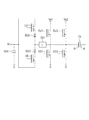
図5は、X電極Xiに接続されるX電極サステイン回路103(図1)の構成例を示す回路図である。Y電極Yiに接続されるY電極サステイン回路104も、X電極サステイン回路103と同様の構成を有するので、X電極サステイン回路103を例に説明する。以下、MOS電界効果トランジスタ(FET)を単にトランジスタという。
FIG. 5 is a circuit diagram showing a configuration example of the X electrode sustain circuit 103 (FIG. 1) connected to the X electrode Xi. Since the Y electrode sustain
X電極Xi及びY電極Yiは、その間に絶縁体を挟み、パネル容量Cpを構成する。nチャネルトランジスタCU1は、ソースがX電極Xiに接続され、ドレインが第1のハイレベルVs1に接続される。nチャネルトランジスタCU2は、ソースがX電極Xiに接続され、ドレインが第2のハイレベルVs2に接続される。nチャネルトランジスタCD1及びCD2は、ソースがグランド(0V)Gに接続され、ドレインがX電極Xiに接続される。 The X electrode Xi and the Y electrode Yi sandwich an insulator between them to constitute a panel capacitance Cp. The n-channel transistor CU1 has a source connected to the X electrode Xi and a drain connected to the first high level Vs1. The n-channel transistor CU2 has a source connected to the X electrode Xi and a drain connected to the second high level Vs2. The n-channel transistors CD1 and CD2 have a source connected to the ground (0V) G and a drain connected to the X electrode Xi.
容量504は、Vcの電位及びグランドG間に接続される。nチャネルトランジスタLUは、ソースがダイオード502のアノードに接続され、ドレインが容量504に接続される。ダイオード502のカソードは、コイル501を介してX電極Xiに接続される。nチャネルトランジスタLDは、ソースが容量504に接続され、ドレインがダイオード502のカソードに接続される。ダイオード503のアノードは、コイル501を介してX電極Xiに接続される。
The
図6(A)は、表示率が大きいときに図5のX電極サステイン回路が生成するサステインパルスであり、図4(A)のサステインパルスに相当する。 FIG. 6A shows a sustain pulse generated by the X electrode sustain circuit in FIG. 5 when the display rate is large, and corresponds to the sustain pulse in FIG.
時刻t601以前では、トランジスタLU、CU1、CU2及びLDはオフ、トランジスタCD1及びCD2はオンである。時刻t601では、トランジスタCD1及びCD2をオフにし、トランジスタLUをオンにする。後に説明するように、容量504は、パネル容量CpのX電極Xiから回収した電力を蓄積している。トランジスタLUがオンになると、容量504の電荷がトランジスタLU及びコイル501を介してLC共振によりX電極Xiに供給される。電位Vcを約Vs1/2に設定すると、X電極Xiの電位は、第1のハイレベルVs1に向けて上昇する。
Prior to time t601, the transistors LU, CU1, CU2, and LD are off, and the transistors CD1 and CD2 are on. At time t601, the transistors CD1 and CD2 are turned off and the transistor LU is turned on. As will be described later, the
次に、時刻t602では、トランジスタCU1をオンにする。すると、第1のハイレベルVs1がX電極Xiに供給され、X電極Xiの電位は第1のハイレベルVs1にクランプされる。 Next, at time t602, the transistor CU1 is turned on. Then, the first high level Vs1 is supplied to the X electrode Xi, and the potential of the X electrode Xi is clamped to the first high level Vs1.
次に、時刻t603では、トランジスタCU2をオンにする。すると、第2のハイレベルVs2がX電極Xiに供給され、X電極Xiの電位は第2のハイレベルVs2にクランプされる。 Next, at time t603, the transistor CU2 is turned on. Then, the second high level Vs2 is supplied to the X electrode Xi, and the potential of the X electrode Xi is clamped to the second high level Vs2.
次に、時刻t604では、トランジスタLU、CU1及びCU2をオフにする。X電極Xiの電位は、第2のハイレベルVs2を維持する。 Next, at time t604, the transistors LU, CU1, and CU2 are turned off. The potential of the X electrode Xi maintains the second high level Vs2.
次に、時刻t605では、トランジスタLDをオンにする。パネル容量CpのX電極Xiの電荷(電力)は、コイル501、トランジスタLDを介してLC共振により容量504に回収され、X電極Xiの電位は低下する。このように、電力回収を行うことにより、消費電力を小さくすることができる。
Next, at time t605, the transistor LD is turned on. The electric charge (power) of the X electrode Xi of the panel capacitance Cp is recovered by the
次に、時刻t606では、トランジスタCD1及びCD2をオンにする。すると、グランドレベルがX電極Xiに接続され、X電極Xiは0Vにクランプされる。 Next, at time t606, the transistors CD1 and CD2 are turned on. Then, the ground level is connected to the X electrode Xi, and the X electrode Xi is clamped to 0V.
次に、時刻t607では、トランジスタLD、CD1及びCD2をオフにする。X電極Xiの電位は、0Vを維持する。 Next, at time t607, the transistors LD, CD1, and CD2 are turned off. The potential of the X electrode Xi is maintained at 0V.
以上の時刻t601〜t607を含むサイクルを1サイクルとして、同じ処理を繰り返す。このサステインパルスは、12μs/サイクルである。例えば、時刻t601からt602までが0.5μs、時刻t602からt603までが0.5μs、時刻t603からt604までが3μs、時刻t604からt605までが1μs、時刻t605からt606までが0.5μs、時刻t606からt607までが5.5μs、時刻t607から次サイクルの時刻t601までが1μsである。 The same process is repeated with one cycle including the above times t601 to t607 as one cycle. This sustain pulse is 12 μs / cycle. For example, 0.5 μs from time t601 to t602, 0.5 μs from time t602 to t603, 3 μs from time t603 to t604, 1 μs from time t604 to t605, 0.5 μs from time t605 to t606, and time t606. To t607 is 5.5 μs, and from time t607 to time t601 of the next cycle is 1 μs.
図6(B)は、表示率が小さいときに図5のX電極サステイン回路が生成するサステインパルスであり、図4(B)のサステインパルスに相当する。 FIG. 6B shows a sustain pulse generated by the X electrode sustain circuit of FIG. 5 when the display rate is small, and corresponds to the sustain pulse of FIG.
時刻t611以前では、トランジスタLU、CU1、CU2及びLDはオフ、トランジスタCD1及びCD2はオンである。時刻t611では、トランジスタCD1及びCD2をオフにし、トランジスタLUをオンにする。後に説明するように、容量504は、パネル容量CpのX電極Xiから回収した電力を蓄積している。トランジスタLUがオンになると、容量504の電荷がトランジスタLU及びコイル501を介してLC共振によりX電極Xiに供給される。電位VcをVs2/2に設定すれば、X電極Xiの電位は、第2のハイレベルVs2に向けて上昇する。
Prior to time t611, the transistors LU, CU1, CU2, and LD are off, and the transistors CD1 and CD2 are on. At time t611, the transistors CD1 and CD2 are turned off and the transistor LU is turned on. As will be described later, the
次に、時刻t612では、トランジスタCU1及びCU2をオンにする。すると、第2のハイレベルVs2がX電極Xiに供給され、X電極Xiの電位は第2のハイレベルVs2にクランプされる。 Next, at time t612, the transistors CU1 and CU2 are turned on. Then, the second high level Vs2 is supplied to the X electrode Xi, and the potential of the X electrode Xi is clamped to the second high level Vs2.
次に、時刻t613では、トランジスタLU、CU1及びCU2をオフにする。X電極Xiの電位は、第2のハイレベルVs2を維持する。 Next, at time t613, the transistors LU, CU1, and CU2 are turned off. The potential of the X electrode Xi maintains the second high level Vs2.
次に、時刻t614では、トランジスタLDをオンにする。パネル容量CpのX電極Xiの電荷(電力)は、コイル501、トランジスタLDを介してLC共振により容量504に回収される。X電極Xiの電位は低下する。このように、電力回収を行うことにより、消費電力を小さくすることができる。
Next, at time t614, the transistor LD is turned on. The charge (electric power) of the X electrode Xi of the panel capacitor Cp is recovered by the
次に、時刻t615では、トランジスタCD1及びCD2をオンにする。すると、グランドレベルがX電極Xiに接続され、X電極Xiは0Vにクランプされる。 Next, at time t615, the transistors CD1 and CD2 are turned on. Then, the ground level is connected to the X electrode Xi, and the X electrode Xi is clamped to 0V.
次に、時刻t616では、トランジスタLD、CD1及びCD2をオフにする。X電極Xiの電位は、0Vを維持する。 Next, at time t616, the transistors LD, CD1, and CD2 are turned off. The potential of the X electrode Xi is maintained at 0V.
以上の時刻t611〜t616を含むサイクルを1サイクルとして、同じ処理を繰り返す。このサステインパルスは、12μs/サイクルである。例えば、時刻t611からt612までが0.5μs、時刻t612からt613までが3.5μs、時刻t613からt614までが1μs、時刻t614からt615までが0.5μs、時刻t615からt616までが5.5μs、時刻t616から次サイクルの時刻t611までが1μsである。
なお、トランジスタCD1及びCD2は、1つのトランジスタで構成してもよい。
The same process is repeated with one cycle including the above times t611 to t616 as one cycle. This sustain pulse is 12 μs / cycle. For example, from time t611 to t612 is 0.5 μs, from time t612 to t613 is 3.5 μs, from time t613 to t614 is 1 μs, from time t614 to t615 is 0.5 μs, from time t615 to t616 is 5.5 μs, The period from time t616 to time t611 of the next cycle is 1 μs.
Note that the transistors CD1 and CD2 may be formed of one transistor.
図7は、表示率と各サブフレームSFのサステインパルスとの関係を示す。図3に示すように、1フレームFRは、例えば10個のサブフレームSF1〜SF10で構成される。サブフレームSF1〜SF10の中で、サブフレームSF1は最もサステインパルス数が少なくて輝度が低く、サブフレームSF10は最もサステインパルス数が多くて輝度が高い。サブフレームSF1からサブフレームSF10に向けて、各サブフレームSFは徐々にサステインパルス数が増加する。 FIG. 7 shows the relationship between the display rate and the sustain pulse of each subframe SF. As shown in FIG. 3, one frame FR is composed of, for example, ten subframes SF1 to SF10. Among the subframes SF1 to SF10, the subframe SF1 has the lowest number of sustain pulses and the luminance is low, and the subframe SF10 has the highest number of sustain pulses and the luminance is high. From the subframe SF1 to the subframe SF10, the number of sustain pulses gradually increases in each subframe SF.
ここで、図4(A)及び図6(A)のように電力を時間的に分散させたサステインパルスを第1のサステインパルスと呼び、図4(B)及び図6(B)のように電力を時間的に集中させたサステインパルスを第2のサステインパルスと呼ぶ。 Here, the sustain pulse in which the power is temporally dispersed as shown in FIGS. 4A and 6A is referred to as a first sustain pulse, as shown in FIGS. 4B and 6B. A sustain pulse in which power is concentrated in time is referred to as a second sustain pulse.
表示率が20〜100%のときには、全てのサブフレームSF1〜SF10において例えば50kHzの第1のサステインパルスを生成する。 When the display rate is 20 to 100%, a first sustain pulse of 50 kHz, for example, is generated in all the subframes SF1 to SF10.
表示率が15%のときには、全てのサブフレームSF1〜SF10において例えば40kHzの第2のサステインパルスを生成する。40kHzの第2のサステインパルスは、50kHzの第1のサステインパルスとほぼ輝度が同じである。ここで、40kHz及び50kHzの周波数は、サステインパルス数を数字的に表現したものであり、周期は同じでもよい。すなわち、表示率が15〜100%の間は、輝度が同じである。これにより、第1のサステインパルスから第2のサステインパルスに切り替える際の輝度の急激な変化を防止することができる。 When the display rate is 15%, for example, a second sustain pulse of 40 kHz is generated in all the subframes SF1 to SF10. The 40 kHz second sustain pulse has substantially the same brightness as the 50 kHz first sustain pulse. Here, the frequencies of 40 kHz and 50 kHz are numerical representations of the number of sustain pulses, and the period may be the same. That is, the luminance is the same when the display rate is 15 to 100%. Thereby, it is possible to prevent an abrupt change in luminance when switching from the first sustain pulse to the second sustain pulse.
すなわち、1フレーム内に第1のサステインパルスで構成されるサブフレームと第2のサステインパルスで構成されるサブフレームとを混在させるときには、その第1のサステインパルスで構成されるサブフレームと第2のサステインパルスで構成されるサブフレームとは輝度がほぼ同じでありかつパルス数が異なる。 That is, when a subframe composed of the first sustain pulse and a subframe composed of the second sustain pulse are mixed in one frame, the subframe composed of the first sustain pulse and the second The luminance is substantially the same as that of the sub-frame composed of the sustain pulses and the number of pulses is different.
ただし、表示率がわずかに違うだけで全てのサブフレームを50kHzの第1のサステインパルスから40kHzの第2のサステインパルスに変化させると、色度が急激に変化し、表示に悪影響を与える。そこで、表示率が15〜20%では、50kHzの第1のサステインパルスで構成されるサブフレームと40kHzの第2のサステインパルスで構成されるサブフレームとを混在させ、徐々に第1及び第2のサステインパルスのサブフレームの比率を変える。 However, if all the sub-frames are changed from the first sustain pulse of 50 kHz to the second sustain pulse of 40 kHz with only a slightly different display rate, the chromaticity changes abruptly and the display is adversely affected. Therefore, when the display rate is 15 to 20%, the subframe composed of the first sustain pulse of 50 kHz and the subframe composed of the second sustain pulse of 40 kHz are mixed, and the first and second are gradually mixed. The ratio of the sustain pulse subframe is changed.
表示率が20%より小さく15%より大きいときには、第1のサステインパルスで構成されるサブフレームSFと第2のサステインパルスで構成されるサブフレームSFとが混在する。表示率が20%よりわずかに小さいときには、1個のサブフレームSF1が40kHzの第2のサステインパルスであり、9個のサブフレームSF2〜SF10が50kHzの第1のサステインパルスである。また、表示率が15%よりわずかに大きいときには、9個のサブフレームSF1〜SF9が40kHzの第2のサステインパルスであり、1個のサブフレームSF10が50kHzの第1のサステインパルスである。表示率が15%から20%の間では、表示率が小さくなるほど、40kHzの第2のサステインパルスで構成されるサブフレームの比率が大きくなる。これにより、表示率がわずかに異なることによる色度の急激な変化を防止することができる。 When the display rate is smaller than 20% and larger than 15%, a subframe SF composed of the first sustain pulse and a subframe SF composed of the second sustain pulse are mixed. When the display rate is slightly smaller than 20%, one subframe SF1 is a second sustain pulse of 40 kHz, and nine subframes SF2 to SF10 are first sustain pulses of 50 kHz. When the display rate is slightly larger than 15%, nine sub-frames SF1 to SF9 are 40 kHz second sustain pulses, and one sub-frame SF10 is a 50 kHz first sustain pulse. When the display rate is between 15% and 20%, the smaller the display rate, the larger the ratio of subframes composed of the second sustain pulse of 40 kHz. Thereby, it is possible to prevent a rapid change in chromaticity due to a slightly different display rate.
表示率が10%から15%までの間では、表示率が小さくなるほど第2のサステインパルスのパルス数を徐々に増加させる。表示率が15%のときには、全てのサブフレームSF1〜SF10において例えば40kHzの第2のサステインパルスを生成するので、比較的輝度が低い。表示率が10%のときには、全てのサブフレームSF1〜SF10において例えば50kHzの第2のサステインパルスを生成するので、比較的輝度が高く、ピーク輝度を高くすることができる。 When the display rate is between 10% and 15%, the number of second sustain pulses is gradually increased as the display rate decreases. When the display rate is 15%, the second sustain pulse of 40 kHz, for example, is generated in all the subframes SF1 to SF10, so that the luminance is relatively low. When the display rate is 10%, the second sustain pulse of 50 kHz, for example, is generated in all the subframes SF1 to SF10, so that the luminance is relatively high and the peak luminance can be increased.
表示率が0〜10%のときには、表示率にかかわらずに50kHzの第2のサステインパルスを生成する。 When the display rate is 0 to 10%, the second sustain pulse of 50 kHz is generated regardless of the display rate.
本実施形態によれば、表示率に応じてサブフレーム単位で表示のための2種類以上のサステインパルスの中から1つを選択して出力するサステインパルス出力部を有する。サステイン出力部は、サステインパルス制御部112、X電極サステイン回路103及びY電極サステイン回路104を含む。各サブフレームにおいて、表示率に応じて第1のサステインパルス又は第2のサステインパルスを選択する。表示率が閾値よりも大きいときには第1のサステインパルスを選択し、表示率が閾値よりも小さいときには第2のサステインパルスを選択する。
According to this embodiment, there is a sustain pulse output unit that selects and outputs one of two or more types of sustain pulses for display in units of subframes according to the display rate. The sustain output unit includes a sustain
具体的には、表示率が第1の閾値20%より大きいときにはフレーム内の全サブフレームが第1のサステインパルスで構成され、表示率が第1の閾値20%より小さいときにはフレーム内に第2のサステインパルスで構成されるサブフレームを含む。表示率が第2の閾値15%より小さいときにはフレーム内の全サブフレームが第2のサステインパルスで構成され、表示率に応じてサブフレームのサステインパルス数を変化させる。表示率が第2の閾値15%より小さく第3の閾値10%より大きいときには、表示率が小さいほど各サブフレームのサステインパルス数が多くなる。表示率が第3の閾値10%より小さいときには、フレーム内の全サブフレームが第2のサステインパルスで構成され、そのサステインパルス数は一定である。第2の閾値は第1の閾値より小さく、第3の閾値は第2の閾値より小さい。
Specifically, when the display rate is larger than the
表示率が第1の閾値20%より小さく第2の閾値15%より大きいときには第1のサステインパルスで構成されるサブフレームと第2のサステインパルスで構成されるサブフレームとを含むフレームが構成され、表示率に応じて1フレーム内において第1のサステインパルスで構成されるサブフレームの数と第2のサステインパルスで構成されるサブフレームの数との比率が変わる。その際、表示率が小さいほど第2のサステインパルスで構成されるサブフレームの数の比率が大きくなる。
When the display rate is smaller than the
発光効率及びストリーキングを改善した第1のサステインパルスでは、第2のサステインパルスよりピーク輝度が低下する。プラズマディスプレイの消費電力は表示率が大きくなるに従って大きくなる。また、ストリーキングは、表示率が大きいラインと表示率が小さいラインとで放電電流が異なり、電圧ドロップによる輝度の差が見えるものであり、表示率が小さいときには問題とならない。通常の画像表示では表示率が約25%以下ではストリーキングは殆ど見えず、15%以下では問題とならない。したがって、上記の表示率の第1の閾値は20%を例に説明したが25%以下が好ましい。 In the first sustain pulse with improved luminous efficiency and streaking, the peak luminance is lower than that in the second sustain pulse. The power consumption of the plasma display increases as the display rate increases. Further, the streaking is not a problem when the display rate is small because the discharge current differs between the line with a high display rate and the line with a low display rate, and a difference in luminance due to voltage drop is visible. In normal image display, streaking is hardly visible when the display rate is about 25% or less, and there is no problem when it is 15% or less. Therefore, although the first threshold value of the display rate is 20% as an example, it is preferably 25% or less.
また表示率20%以下ではサステイン放電による消費電力が小さいため、必ずしも発光効率を改善する第1のサステインパルスでなくても良い。また、ピーク輝度はガラスの反射やヘッドライトの煌めき等の比較的暗い画像内での高輝度画素で目立ち、表示率10%以下、特に5%以下でピーク輝度が要求される。したがって、上記の表示率の第3の閾値は10%を例に説明したが5%以上が好ましい。 Further, when the display rate is 20% or less, the power consumption due to the sustain discharge is small, and therefore the first sustain pulse for improving the light emission efficiency is not necessarily required. The peak luminance is conspicuous in high-luminance pixels in a relatively dark image such as glass reflection or headlight flickering, and the peak luminance is required at a display rate of 10% or less, particularly 5% or less. Therefore, the third threshold value of the display rate has been described by taking 10% as an example, but 5% or more is preferable.
以上のように、1フレームFRは、例えば10サブフレームSF1〜SF10からなる。各サブフレームSFは、リセット期間Tr、アドレス期間Ta、電荷調整サステイン期間Tc、サステイン期間Tsで構成される。サステイン期間Tsにおいて、第1のサステインパルスは図6(A)の2段放電波形、第2のサステインパルスは図6(B)の通常放電波形の繰り返しで構成される。各サブフレームSFの輝度重みは、第1のサブフレームSF1が最も輝度が低く、第10のサブフレームSF10が最も輝度が高くなっている。第1及び第2のサステインパルスの立ち上げ及び立ち下げは、LC共振による電力回収回路(パワーセーブ回路)を用いる。第1のサステインパルスのサブフレームと第2のサステインパルスのサブフレームでは、同じ階調でもサステインパルス数を変える。第1のサステインパルスはサステインパルス数が多く、即ち周波数を高くし、各サブフレームSFの輝度をほぼ同じにしてある。画像データ又は消費電力(消費電流)から表示率を計算又は推定し、表示率が20%以上では第1のサステインパルスのサブフレームで表示し、20%から15%の間では第1のサステインパルスのサブフレームから順番に第2のサステインパルスのサブフレームに切り替え、表示率が15%以下では全てのサブフレームが第2のサステインパルスとなる。最高サステインパルス数は、表示率が15%から10%に変わる間で表示率に逆比例して高くし、表示率が10%以下では表示率が15%以上のときより高い状態で一定とする。本実施形態では、第1のサステインパルスの最高輝度のパルス数(周波数)は50kHz、第2のサステインパルスのサブフレーム切り替え途中の最高輝度のパルス数(周波数)は40kHz、表示率が10%以下での最高輝度のパルス数(周波数)は50kHzである。 As described above, one frame FR includes, for example, 10 subframes SF1 to SF10. Each subframe SF includes a reset period Tr, an address period Ta, a charge adjustment sustain period Tc, and a sustain period Ts. In the sustain period Ts, the first sustain pulse is configured by repeating the two-stage discharge waveform of FIG. 6A, and the second sustain pulse is a repetition of the normal discharge waveform of FIG. 6B. The luminance weight of each subframe SF has the lowest luminance in the first subframe SF1 and the highest luminance in the tenth subframe SF10. The first and second sustain pulses are raised and lowered using a power recovery circuit (power save circuit) based on LC resonance. In the first sustain pulse subframe and the second sustain pulse subframe, the number of sustain pulses is changed even in the same gradation. The first sustain pulse has a large number of sustain pulses, that is, the frequency is increased, and the luminance of each subframe SF is substantially the same. A display rate is calculated or estimated from image data or power consumption (current consumption). When the display rate is 20% or more, it is displayed in the first sustain pulse subframe, and when it is between 20% and 15%, the first sustain pulse is displayed. The sub-frames of the second sustain pulse are switched to the sub-frames of the second sustain pulse in order, and when the display rate is 15% or less, all the sub-frames become the second sustain pulses. The maximum number of sustain pulses is increased in inverse proportion to the display rate while the display rate is changed from 15% to 10%, and is constant when the display rate is 10% or less and higher than when the display rate is 15% or more. . In this embodiment, the pulse number (frequency) of the highest brightness of the first sustain pulse is 50 kHz, the pulse number (frequency) of the highest brightness during subframe switching of the second sustain pulse is 40 kHz, and the display rate is 10% or less. The number of pulses with the highest luminance (frequency) is 50 kHz.
本実施形態によれば、発光効率/ストリーキングが問題となる表示状態では第1のサステインパルスで表示するため、発光効率が高く、ストリーキングも少ない。第1のサステインパルスのままでは表示率が小さい場合でも最高輝度が約800cd/m2であるが、発光効率/ストリーキングが殆ど問題とならない表示状態では第2のサステインパルスを用い、第2のサステインパルスはパルス数(周波数)を50kHz以上にすることができるので、さらに高い輝度(ピーク)が実現可能である。表示率が小さい場合の最高輝度は約1000cd/m2と高いピーク輝度で表示できる。同じ輝度の約800cd/m2のサブフレームで第1のサステインパルスから第2のサステインパルスに切り替えるので輝度の切り替えショックはなく、またサブフレーム単位で少しずつ切り替えるので、色度の切り替えショックも殆どない。更に、サブフレームは階調の軽い、輝度の小さい順番から切り替えるので、サステインパルスの種類の切り替えが発光効率/ストリーキングに与える影響はより小さくなる。すなわち、1フレームは輝度が異なる複数のサブフレームを含み、1フレーム内に第1のサステインパルスで構成されるサブフレームと第2のサステインパルスで構成されるサブフレームとを混在させるときには、輝度が低いサブフレームを優先して第2のサステインパルスで構成するサブフレームとする。表示率によりサステイン周波数やサブフレームを切り替える場合、頻繁な切り替えを防止するため、通常はヒステリシスを持たせる。 According to the present embodiment, since the display is performed with the first sustain pulse in the display state where the light emission efficiency / streaking is a problem, the light emission efficiency is high and the streaking is small. Even if the display rate is small with the first sustain pulse, the maximum luminance is about 800 cd / m 2 , but the second sustain pulse is used in the display state in which the light emission efficiency / streaking hardly becomes a problem. Since the number of pulses (frequency) of the pulses can be 50 kHz or more, higher luminance (peak) can be realized. When the display rate is small, the maximum luminance can be displayed with a high peak luminance of about 1000 cd / m 2 . Since the first sustain pulse is switched to the second sustain pulse in the sub-frame of about 800 cd / m 2 with the same luminance, there is no luminance switching shock, and since the switching is performed little by little in units of sub-frames, there is almost no chromaticity switching shock. Absent. Furthermore, since the sub-frames are switched in the order of light gradation and in ascending order of luminance, the influence of switching the type of the sustain pulse on the light emission efficiency / streaking is further reduced. That is, one frame includes a plurality of subframes having different luminances. When a subframe composed of the first sustain pulse and a subframe composed of the second sustain pulse are mixed in one frame, the luminance is A subframe composed of the second sustain pulse is given priority to the lower subframe. When switching the sustain frequency or subframe depending on the display rate, a hysteresis is usually provided to prevent frequent switching.
本実施形態では、輝度の低いサブフレームから輝度の高いサブフレームの順番に配列しているが、画質向上のため階調の順番を入れ替えることがあるが、その場合も輝度の低いサブフレームよりサステインパルスの種類を切り替えた方がストリーキングや発光効率への影響を小さくできる。 In this embodiment, the subframes are arranged in the order of the subframes with the low luminance to the subframes with the high luminance. However, in order to improve the image quality, the order of the gradation may be changed. Switching the pulse type can reduce the effect on streaking and luminous efficiency.
(第2の実施形態)
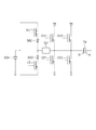
図8は、本発明の第2の実施形態によるX電極サステイン回路103(図1)の構成例を示す回路図である。図8の回路は、図5の回路に代わる回路であり、図5の回路と異なる点を説明する。トランジスタCU1のドレインは、第1のハイレベルVs1の代わりにハイレベルVsに接続される。トランジスタCU2のドレインは、第2のハイレベルVs2の代わりにハイレベルVsに接続される。容量504は、電力回収により約Vs/2となり、必ずしもVs/2の電位に接続する必要はない。
(Second Embodiment)
FIG. 8 is a circuit diagram showing a configuration example of the X electrode sustain circuit 103 (FIG. 1) according to the second embodiment of the present invention. The circuit of FIG. 8 is a circuit that replaces the circuit of FIG. 5 and will be described with respect to differences from the circuit of FIG. The drain of the transistor CU1 is connected to the high level Vs instead of the first high level Vs1. The drain of the transistor CU2 is connected to the high level Vs instead of the second high level Vs2. The
図9(A)は、表示率が大きいときに図8のX電極サステイン回路が生成するサステインパルスである。 FIG. 9A shows a sustain pulse generated by the X electrode sustain circuit of FIG. 8 when the display rate is large.
時刻t901以前では、トランジスタLU、CU1、CU2及びLDはオフ、トランジスタCD1及びCD2はオンである。時刻t901では、トランジスタCD1及びCD2をオフにし、トランジスタLUをオンにする。後に説明するように、容量504は、パネル容量CpのX電極Xiから回収した電力を蓄積している。トランジスタLUがオンになると、容量504の電荷がトランジスタLU及びコイル501を介してLC共振によりX電極Xiに供給される。X電極Xiの電位は、ハイレベルVsに向けて上昇する。
Prior to time t901, the transistors LU, CU1, CU2, and LD are off, and the transistors CD1 and CD2 are on. At time t901, the transistors CD1 and CD2 are turned off and the transistor LU is turned on. As will be described later, the
次に、時刻t902では、トランジスタCU1をオンにする。トランジスタCU2はオフであるので、ハイインピーダンスでハイレベルVsがX電極Xiに供給され、X電極Xiの電位はハイレベルVsにクランプされる。 Next, at time t902, the transistor CU1 is turned on. Since the transistor CU2 is off, the high level Vs is supplied to the X electrode Xi with high impedance, and the potential of the X electrode Xi is clamped to the high level Vs.
次に、時刻t903では、トランジスタCU2をオンにする。トランジスタCU1もオンであるので、ローインピーダンスでハイレベルVsがX電極Xiに供給され、X電極Xiの電位はハイレベルVsにクランプされる。 Next, at time t903, the transistor CU2 is turned on. Since the transistor CU1 is also on, the high level Vs is supplied to the X electrode Xi with low impedance, and the potential of the X electrode Xi is clamped to the high level Vs.
次に、時刻t904では、トランジスタLU、CU1及びCU2をオフにする。X電極Xiの電位は、ハイレベルVsを維持する。 Next, at time t904, the transistors LU, CU1, and CU2 are turned off. The potential of the X electrode Xi maintains the high level Vs.
次に、時刻t905では、トランジスタLDをオンにする。パネル容量CpのX電極Xiの電荷(電力)は、コイル501、トランジスタLDを介してLC共振により容量504に回収される。X電極Xiの電位は低下する。このように、電力回収を行うことにより、消費電力を小さくすることができる。
Next, at time t905, the transistor LD is turned on. The charge (electric power) of the X electrode Xi of the panel capacitor Cp is recovered by the
次に、時刻t906では、トランジスタCD1をオンにする。トランジスタCD2はオフであるので、ハイインピーダンスでグランドレベルがX電極Xiに接続され、X電極Xiは0Vにクランプされる。 Next, at time t906, the transistor CD1 is turned on. Since the transistor CD2 is off, the ground level is connected to the X electrode Xi with high impedance, and the X electrode Xi is clamped to 0V.
次に、時刻t907では、トランジスタCD2をオンにする。トランジスタCD1もオンであるので、ローレベルでグランドレベルがX電極Xiに接続され、X電極Xiは0Vにクランプされる。 Next, at time t907, the transistor CD2 is turned on. Since the transistor CD1 is also on, the ground level is connected to the X electrode Xi at a low level, and the X electrode Xi is clamped to 0V.
次に、時刻t908では、トランジスタLD、CD1及びCD2をオフにする。X電極Xiの電位は、0Vを維持する。 Next, at time t908, the transistors LD, CD1, and CD2 are turned off. The potential of the X electrode Xi is maintained at 0V.
以上の時刻t901〜t908を含むサイクルを1サイクルとして、同じ処理を繰り返す。このサステインパルスは、12μs/サイクルである。例えば、時刻t901からt902までが0.5μs、時刻t902からt903までが0.5μs、時刻t903からt904までが3μs、時刻t904からt905までが1μs、時刻t905からt906までが0.5μs、時刻t906からt907までが0.5μs、時刻t907からt908までが5μs、時刻t908から次サイクルの時刻t901までが1μsである。 The same process is repeated with one cycle including the above times t901 to t908 as one cycle. This sustain pulse is 12 μs / cycle. For example, 0.5 μs from time t901 to t902, 0.5 μs from time t902 to t903, 3 μs from time t903 to t904, 1 μs from time t904 to t905, 0.5 μs from time t905 to t906, and time t906 From time t907 to t907 is 0.5 μs, from time t907 to t908 is 5 μs, and from time t908 to time t901 of the next cycle is 1 μs.
上記の時刻t902〜t903では、X電極XiがハイインピーダンスでハイレベルVsにクランプされるので、弱い放電が発生する。そして、時刻t903以降では、X電極XiがローインピーダンスでハイレベルVsにクランプされるので、放電が継続して発生する。このサステインパルスは、電力を時間的に分散させたサステインパルスであるため、放電電流の時間的幅が広くなり、放電電流のピークが小さくなる。その結果、放電強度が小さくなるために紫外線発光及び蛍光体の飽和が小さくなって発光効率が高くなり、かつ放電電流ピークが小さいためにストリーキングを低減させることができる。 At times t902 to t903, the X electrode Xi is clamped at the high level Vs with high impedance, so that weak discharge occurs. Then, after time t903, the X electrode Xi is clamped to the high level Vs with low impedance, and thus discharge continues. Since the sustain pulse is a sustain pulse in which power is dispersed in time, the time width of the discharge current is widened, and the peak of the discharge current is reduced. As a result, since the discharge intensity is reduced, ultraviolet light emission and phosphor saturation are reduced, the luminous efficiency is increased, and the discharge current peak is small, so that streaking can be reduced.
図9(B)は、表示率が小さいときに図8のX電極サステイン回路が生成するサステインパルスである。 FIG. 9B shows a sustain pulse generated by the X electrode sustain circuit of FIG. 8 when the display rate is small.
時刻t911以前では、トランジスタLU、CU1、CU2及びLDはオフ、トランジスタCD1及びCD2はオンである。時刻t911では、トランジスタCD1及びCD2をオフにし、トランジスタLUをオンにする。後に説明するように、容量504は、パネル容量CpのX電極Xiから回収した電力を蓄積している。トランジスタLUがオンになると、容量504の電荷がトランジスタLU及びコイル501を介してLC共振によりX電極Xiに供給される。X電極Xiの電位は、ハイレベルVsに向けて上昇する。
Prior to time t911, the transistors LU, CU1, CU2, and LD are off, and the transistors CD1 and CD2 are on. At time t911, the transistors CD1 and CD2 are turned off and the transistor LU is turned on. As will be described later, the
次に、時刻t912では、トランジスタCU1及びCU2をオンにする。すると、ローインピーダンスでハイレベルVsがX電極Xiに供給され、X電極Xiの電位はハイレベルVsにクランプされる。 Next, at time t912, the transistors CU1 and CU2 are turned on. Then, the high level Vs is supplied to the X electrode Xi with low impedance, and the potential of the X electrode Xi is clamped to the high level Vs.
次に、時刻t913では、トランジスタLU、CU1及びCU2をオフにする。X電極Xiの電位は、ハイレベルVsを維持する。 Next, at time t913, the transistors LU, CU1, and CU2 are turned off. The potential of the X electrode Xi maintains the high level Vs.
次に、時刻t914では、トランジスタLDをオンにする。パネル容量CpのX電極Xiの電荷(電力)は、コイル501、トランジスタLDを介してLC共振により容量504に回収される。X電極Xiの電位は低下する。このように、電力回収を行うことにより、消費電力を小さくすることができる。
Next, at time t914, the transistor LD is turned on. The charge (electric power) of the X electrode Xi of the panel capacitor Cp is recovered by the
次に、時刻t915では、トランジスタCD1及びCD2をオンにする。すると、グランドレベルがX電極Xiに接続され、X電極Xiは0Vにクランプされる。 Next, at time t915, the transistors CD1 and CD2 are turned on. Then, the ground level is connected to the X electrode Xi, and the X electrode Xi is clamped to 0V.
次に、時刻t916では、トランジスタLD、CD1及びCD2をオフにする。X電極Xiの電位は、0Vを維持する。 Next, at time t916, the transistors LD, CD1, and CD2 are turned off. The potential of the X electrode Xi is maintained at 0V.
以上の時刻t911〜t916を含むサイクルを1サイクルとして、同じ処理を繰り返す。このサステインパルスは、12μs/サイクルである。例えば、時刻t911からt912までが0.5μs、時刻t912からt913までが3.5μs、時刻t913からt914までが1μs、時刻t914からt915までが0.5μs、時刻t915からt916までが5.5μs、時刻t916から次サイクルの時刻t911までが1μsである。 The same process is repeated with one cycle including the above times t911 to t916 as one cycle. This sustain pulse is 12 μs / cycle. For example, from time t911 to t912 is 0.5 μs, from time t912 to t913 is 3.5 μs, from time t913 to t914 is 1 μs, from time t914 to t915 is 0.5 μs, from time t915 to t916 is 5.5 μs, The period from time t916 to time t911 of the next cycle is 1 μs.
上記の時刻t912では、X電極XiがローインピーダンスでハイレベルVsにクランプされるので、強い放電が発生する。このサステインパルスは、電力を時間的に集中させたサステインパルスであるため、放電電流の時間的幅が狭くなり、放電電流のピークが大きくなる。その結果、ピーク輝度が高くなる。 At the time t912, the X electrode Xi is clamped to the high level Vs with low impedance, so that strong discharge occurs. Since the sustain pulse is a sustain pulse in which power is concentrated in time, the time width of the discharge current is narrowed and the peak of the discharge current is increased. As a result, the peak luminance is increased.
以上のように、本実施形態では、表示率が大きいときはLC共振で電圧を立ち上げた後にハイレベルVsへの電圧クランプをハイインピーダンス及びローインピーダンスの2段階に行い、表示率の小さいときはトランジスタCU1及びCU2を同時にオンしてクランプする。図9(A)の2段クランプの場合は、放電はLC共振で電圧が立ち上がった直後に発生するが、電圧クランプのトランジスタCU1の電流容量が小さく、インピーダンスが高いために放電電流が制限され、パネル電極抵抗による電圧ドロップは軽減され、ストリーキングは改善される。しかし、放電電流が制限されるため、サステインパルス1発当たりの輝度が低下し、ピーク輝度も低下する。図9(B)のように、トランジスタCU1及びCU2を同時に立ち上げた場合は、放電時のインピーダンスが低く大きな放電電流が流れるため輝度が高くなるが、電極抵抗による電圧ドロップのためストリーキングが大きい。 As described above, in this embodiment, when the display ratio is large, the voltage is raised to the high level Vs after the voltage is raised by the LC resonance, and the two levels of high impedance and low impedance are performed. Transistors CU1 and CU2 are turned on and clamped simultaneously. In the case of the two-stage clamp in FIG. 9A, discharge occurs immediately after the voltage rises due to LC resonance, but the current capacity of the voltage clamp transistor CU1 is small and the impedance is high, so the discharge current is limited. Voltage drop due to panel electrode resistance is reduced and streaking is improved. However, since the discharge current is limited, the luminance per sustain pulse is lowered and the peak luminance is also lowered. As shown in FIG. 9B, when the transistors CU1 and CU2 are activated at the same time, the luminance is high because of a low impedance during discharge and a large discharge current flows, but the streaking is large because of voltage drop due to electrode resistance.
本実施形態は、図9(A)に示すようにストリーキングが問題となる表示率が大きいときは複数のトランジスタCU1及びCU2による立ち上げを分けて2段でクランプし、図9(B)に示すようにストリーキングがあまり問題とならない表示率の小さいときは複数のトランジスタCU1及びCU2により同時にクランプする。サステインパルスの種類の切り替えは輝度の同じサブフレーム単位で行い、表示率が下がって全てのサブフレームが同時クランプに切り替わってから、表示率が下がるに従い徐々にパルス数を多くして高いピーク輝度が出せる状態にする。本実施形態によれば、ストリーキングが問題となる表示状態ではストリーキングが小さくて発光効率が高い第1のサステインパルスを用い、ストリーキングが殆ど問題とならない表示状態では輝度を優先した第2のサステインパルスを用いることにより高いピーク輝度で表示ができる。 In this embodiment, as shown in FIG. 9A, when the display rate causing streaking is a problem, the rise by the plurality of transistors CU1 and CU2 is divided and clamped in two stages, as shown in FIG. 9B. As described above, when the display rate is small, where streaking is not a significant problem, clamping is performed simultaneously by the plurality of transistors CU1 and CU2. The type of sustain pulse is switched in units of sub-frames with the same brightness. After the display rate has decreased and all sub-frames have been switched to simultaneous clamping, the number of pulses gradually increases as the display rate decreases, resulting in high peak luminance. Make it ready. According to the present embodiment, in the display state where streaking is a problem, the first sustain pulse having a small streaking and high luminous efficiency is used, and in the display state where the streaking is hardly a problem, the second sustain pulse giving priority to luminance is used. By using it, it is possible to display with high peak luminance.
本実施形態では、複数のトランジスタCU1及びCU2により複数段に立ち上げたが、LC共振による電圧立ち上げから遅らせてから電圧クランプ用のトランジスタ(出力素子)を立ち上げてもよい。また、トランジスタCU1及びCU2のゲート抵抗を高くしてトランジスタのオン直後の出力抵抗を高くしても同様な効果が得られる。 In the present embodiment, the transistors are raised in a plurality of stages by the plurality of transistors CU1 and CU2. However, the voltage clamping transistor (output element) may be activated after delaying the voltage rise by the LC resonance. The same effect can be obtained even if the gate resistance of the transistors CU1 and CU2 is increased to increase the output resistance immediately after the transistors are turned on.
(第3の実施形態)
本発明の第3の実施形態では、表示率が大きいときには図10(A)のサステインパルスを生成し、表示率が小さいときには図10(B)のサステインパルスを生成する。
(Third embodiment)
In the third embodiment of the present invention, the sustain pulse shown in FIG. 10A is generated when the display rate is high, and the sustain pulse shown in FIG. 10B is generated when the display rate is low.
図10(A)は、表示率が大きいときのX電極Xi及びY電極Yiのサステインパルスを示すタイミングチャートである。図10(B)は、表示率が小さいときのX電極Xi及びY電極Yiのサステインパルスを示すタイミングチャートである。図1のY電極サステイン回路104は、サステインパルス制御部112の制御の下、表示率が大きいときには図10(A)に示すサステインパルスを生成し、表示率が小さいときには図10(B)に示すサステインパルスを生成する。図10(A)及び(B)のサステインパルスは、図3のサステイン期間Tsにおいて生成される。
FIG. 10A is a timing chart showing sustain pulses of the X electrode Xi and the Y electrode Yi when the display rate is large. FIG. 10B is a timing chart showing a sustain pulse of the X electrode Xi and the Y electrode Yi when the display rate is small. The Y electrode sustain
図10(A)のX電極Xi及びY電極Yiのサステインパルスは、時刻t1001からt1006までを含むサイクルを1サイクルとして、パルスが繰り返される。 In the sustain pulse of the X electrode Xi and the Y electrode Yi in FIG. 10A, the cycle including the time t1001 to t1006 is one cycle, and the pulse is repeated.
まず、図10(A)のX電極Xiのサステインパルスを説明する。時刻t1001では、0Vのローレベルから立ち上がってそれよりも高い第2のハイレベルVs2にクランプされる。次に、時刻t1002では、第2のハイレベルVs2から立ち下がってそれよりも低い第1のハイレベルVs1にクランプされる。次に、時刻t1003では、第1のハイレベルVs1から立ち下がって0Vのローレベルにクランプされる。以後、1サイクルの終わりまで、0Vのローレベルを維持する。 First, the sustain pulse of the X electrode Xi in FIG. At time t1001, the voltage rises from the low level of 0V and is clamped to the second high level Vs2 higher than that. Next, at time t1002, the signal falls from the second high level Vs2 and is clamped to the first high level Vs1 lower than that. Next, at time t1003, the voltage falls from the first high level Vs1 and is clamped to a low level of 0V. Thereafter, the low level of 0 V is maintained until the end of one cycle.
次に、図10(A)のY電極Yiのサステインパルスを説明する。時刻t1001からt1004の直前までは、0Vのローレベルを維持する。時刻t1004では、0Vのローレベルから立ち上がってそれよりも高い第2のハイレベルVs2にクランプされる。次に、時刻t1005では、第2のハイレベルVs2から立ち下がってそれよりも低い第1のハイレベルVs1にクランプされる。次に、時刻t1006では、第1のハイレベルVs1から立ち下がって0Vのローレベルにクランプされる。以後、1サイクルの終わりまで、0Vのローレベルを維持する。 Next, the sustain pulse of the Y electrode Yi in FIG. From time t1001 to immediately before t1004, the low level of 0V is maintained. At time t1004, the voltage rises from the low level of 0V and is clamped to the second high level Vs2 higher than that. Next, at time t1005, the signal falls from the second high level Vs2 and is clamped to the first high level Vs1 lower than that. Next, at time t1006, the voltage falls from the first high level Vs1 and is clamped to a low level of 0V. Thereafter, the low level of 0 V is maintained until the end of one cycle.
このサステインパルスは、例えば12μs/サイクルである。上記の時刻t1001及びt1004では、X電極Xi及びY電極Yi間に短時間だけ電位差Vs2が生じ、弱い放電が発生する。そして、時刻t1002及びt1005以降では、X電極Xi及びY電極Yi間に電位差Vs1が生じ、放電が継続して発生する。このサステインパルスは、電力を時間的に分散させたサステインパルスであるため、放電電流の時間的幅が広くなり、放電電流のピークが小さくなる。その結果、放電強度が小さくなるために紫外線発光及び蛍光体の飽和が小さくなって発光効率が高くなり、かつ放電電流ピークが小さいためにストリーキングを低減させることができる。 This sustain pulse is, for example, 12 μs / cycle. At the times t1001 and t1004, the potential difference Vs2 is generated between the X electrode Xi and the Y electrode Yi for a short time, and a weak discharge is generated. Then, after time t1002 and t1005, a potential difference Vs1 is generated between the X electrode Xi and the Y electrode Yi, and discharge is continuously generated. Since the sustain pulse is a sustain pulse in which power is dispersed in time, the time width of the discharge current is widened, and the peak of the discharge current is reduced. As a result, since the discharge intensity is reduced, ultraviolet light emission and phosphor saturation are reduced, the luminous efficiency is increased, and the discharge current peak is small, so that streaking can be reduced.
図10(B)のX電極Xi及びY電極Yiのサステインパルスは、時刻t1011からt1014までを含むサイクルを1サイクルとして、パルスが繰り返される。このサステインパルスは、図4(B)のサステインパルスと同じパルスである。図10(B)の時刻t1011〜t1014は、図4(B)の時刻t411〜t414に相当する。 The sustain pulse of the X electrode Xi and the Y electrode Yi in FIG. 10B is repeated with one cycle including the time t1011 to t1014 as one cycle. This sustain pulse is the same pulse as the sustain pulse in FIG. Times t1011 to t1014 in FIG. 10B correspond to times t411 to t414 in FIG.
このサステインパルスは、例えば12μs/サイクルである。上記の時刻t1011及びt1013では、X電極Xi及びY電極Yi間に長時間にわたって電位差Vs2が生じ、強い放電が発生する。このサステインパルスは、電力を時間的に集中させたサステインパルスであるため、放電電流の時間的幅が狭くなり、放電電流のピークが大きくなる。その結果、ピーク輝度が高くなる。 This sustain pulse is, for example, 12 μs / cycle. At the above-mentioned times t1011 and t1013, a potential difference Vs2 is generated for a long time between the X electrode Xi and the Y electrode Yi, and a strong discharge is generated. Since the sustain pulse is a sustain pulse in which power is concentrated in time, the time width of the discharge current is narrowed and the peak of the discharge current is increased. As a result, the peak luminance is increased.
以上のように、第1〜第3の実施形態によれば、高発光効率/ストリーキング低減と高輝度等の異なる複数の特性を実現するためには2種類以上のサステインパルスが必要になる。しかし、サステインパルスの種類により放電/壁電荷等の状態が異なるため、サステイン期間Ts内で切り替えると表示異常が発生する事があるが、リセット期間Ts及び電荷調整サステイン期間Tcを入れれば、即ち、サブフレーム単位でサステインパルスを変えれば動作上の問題は発生しない。また、サブフレーム単位であれば、サステインパルスを個別に設定する事が比較的容易である。 As described above, according to the first to third embodiments, two or more types of sustain pulses are required to realize a plurality of different characteristics such as high luminous efficiency / reducing streaking and high luminance. However, since the state of discharge / wall charge or the like varies depending on the type of the sustain pulse, a display abnormality may occur when switching within the sustain period Ts. However, if the reset period Ts and the charge adjustment sustain period Tc are included, that is, If the sustain pulse is changed in units of subframes, no operational problem occurs. Further, in the case of subframe units, it is relatively easy to set the sustain pulse individually.
本実施形態では、表示率が比較的大きく発光効率/ストリーキングが問題となるときには発光効率/ストリーキング対策のための第1のサステインパルスで表示し、表示率が比較的小さく発光効率/ストリーキングが問題とならないときには高輝度表示ができる第2のサステインパルスで表示する。この際、リセット期間Tsや電荷調整サステイン期間Tc等を有するサブレーム単位で順次サステインパルスを切り替える。サステインパルスの種類により同じパルス数でも輝度が異なるため、サブフレームの切り替えショックがある場合は、サステインパルス数を変えて同じ輝度のサブフレームで切り替えを行い、全てのサブフレームが切り替わった後で、表示率によりサステインパルス数を徐々に多くして高いピーク輝度が出せるようにする。 In the present embodiment, when the display rate is relatively large and the luminous efficiency / streaking is a problem, the display is displayed with the first sustain pulse as a countermeasure against the luminous efficiency / streaking, and the display rate is relatively small and the luminous efficiency / streaking is a problem. If not, the display is performed with the second sustain pulse capable of high brightness display. At this time, the sustain pulse is sequentially switched in units of subframes having a reset period Ts, a charge adjustment sustain period Tc, and the like. Even if the number of pulses is the same, the brightness varies depending on the type of sustain pulse, so if there is a subframe switching shock, change the number of sustain pulses and switch at the same luminance subframe, and after all subframes have switched, The number of sustain pulses is gradually increased according to the display rate so that high peak luminance can be obtained.
本実施形態によれば、発光効率及びストリーキングが問題となる表示状態(例えば表示率20%以上)では図6(A)、図9(A)及び図10(A)等の電力を時間的に集中させた第1のサステインパルスを使用する。表示率が小さいため発光効率が問題とならず、各ラインの表示負荷による電圧ドロップが小さくストリーキングがあまり問題とならない表示状態(例えば表示率15%以下)では、高輝度表示ができる第2のサステインパルスを使用する。第2のサステインパルスは、図6(B)、図9(B)及び図10(B)等の電力を時間的に分散させたサステインパルスである。 According to the present embodiment, in the display state where the light emission efficiency and streaking are problems (for example, the display rate is 20% or more), the power of FIG. 6 (A), FIG. 9 (A), FIG. A concentrated first sustain pulse is used. Since the display rate is small, the luminous efficiency does not become a problem, and in the display state where the voltage drop due to the display load of each line is small and the streaking is not a serious problem (for example, a display rate of 15% or less), the second sustain capable of high brightness display. Use pulses. The second sustain pulse is a sustain pulse in which the power shown in FIGS. 6B, 9B, and 10B is temporally dispersed.
また、動作安定性の確保と制御の容易性のため、リセット期間Tr及び電荷調整サステイン期間Tc等を含むサブフレーム単位でサステインパルスの種類を切り替える。サステインパルスの切り替えに伴う輝度及び色度等の切り替えショックを軽減するため、表示率を検出して徐々にサステインパルスの種類をサブフレーム単位で切り替える。輝度の切り替えショックを更に軽減するためには、同一輝度の異なる種類のサステインパルスのサブフレームに切り替えた後で、表示率を検出して徐々にサステインパルス数を多くして高いピーク輝度が出せる状態にする。これにより、表示率に応じて2種類以上のサステインパルスの中から1つを選択して出力することができ、動作が安定で制御が容易なサブフレーム単位の切り替えでサステインパルスの種類の切り替えショックもない。 In order to ensure operation stability and ease of control, the type of sustain pulse is switched in units of subframes including the reset period Tr and the charge adjustment sustain period Tc. In order to reduce switching shocks such as luminance and chromaticity due to switching of the sustain pulse, the display rate is detected and the type of the sustain pulse is gradually switched in units of subframes. In order to further reduce the luminance switching shock, after switching to a different type of sustain pulse sub-frame of the same luminance, the display rate is detected and the number of sustain pulses can be gradually increased to produce a high peak luminance. To. As a result, it is possible to select and output one of two or more types of sustain pulses according to the display rate, and to switch the type of sustain pulse by switching in subframe units, which is stable and easy to control. Nor.
なお、上記の第1〜第3の実施形態において、図1の表示率検出部111及びサステインパルス制御部112を含む制御回路部101は、ハードウエアにより構成してもよいし、コンピュータプログラムによるソフトウエアをマイクロコンピュータ等が実行することにより構成してもよい。
In the first to third embodiments described above, the
また、第1〜第3の実施形態では、表示率を検出してサステインパルスの種類を切り替えたが、表示率に限定されず、ストリーキングの出やすい表示パターン等の表示状態を検出してサステインパルスを切り替えても良い。その場合は、検出部111が表示状態を検出する。また、発光効率/ストリーキングの優れたサステインパルスとピーク輝度の高いサステインパルスの代わりに、例えば表示率が大きい表示状態では色純度がよく階調特性の良いサステインパルス、表示率が小さい状態では輝度の高くできるサステインパルスに切り替えても良い。 In the first to third embodiments, the display rate is detected and the type of the sustain pulse is switched. However, the display pulse is not limited to the display rate, and the sustain pulse is detected by detecting the display state such as a display pattern that is likely to cause streaking. May be switched. In that case, the detection unit 111 detects the display state. Also, instead of a sustain pulse with excellent luminous efficiency / streaking and a sustain pulse with high peak luminance, for example, a sustain pulse with good color purity and good gradation characteristics in a display state with a high display rate, and a luminance with a low display rate. It may be switched to a sustain pulse that can be increased.
上記実施形態は、何れも本発明を実施するにあたっての具体化の例を示したものに過ぎず、これらによって本発明の技術的範囲が限定的に解釈されてはならないものである。すなわち、本発明はその技術思想、またはその主要な特徴から逸脱することなく、様々な形で実施することができる。 The above-described embodiments are merely examples of implementation in carrying out the present invention, and the technical scope of the present invention should not be construed as being limited thereto. That is, the present invention can be implemented in various forms without departing from the technical idea or the main features thereof.
本発明の実施形態は、例えば以下のように種々の適用が可能である。 The embodiment of the present invention can be applied in various ways as follows, for example.
(付記1)
1フレーム画像を複数のサブフレームにて構成した表示装置であって、
表示状態を検出する検出部と、
前記表示状態に応じてサブフレーム単位で表示のための2種類以上のサステインパルスの中から1つを選択して出力するサステインパルス出力部と
を有する表示装置。
(付記2)
前記2種類以上のサステインパルスは、電力を時間的に分散させた第1のサステインパルスと、電力を時間的に集中させた第2のサステインパルスとを含む付記1記載の表示装置。
(付記3)
前記表示状態は表示率であり、
前記サステインパルス出力部は、前記表示率が閾値よりも大きいときには前記第1のサステインパルスを選択して出力し、前記表示率が閾値よりも小さいときには前記第2のサステインパルスを選択して出力する付記2記載の表示装置。
(付記4)
前記表示率が第1の閾値より大きいときにはフレーム内の全サブフレームが第1のサステインパルスで構成され、前記表示率が第1の閾値より小さいときにはフレーム内に第2のサステインパルスで構成されるサブフレームを含む付記3記載の表示装置。
(付記5)
前記表示率が第2の閾値より小さいときにはフレーム内の全サブフレームが第2のサステインパルスで構成される付記4記載の表示装置。
(付記6)
前記表示率が第2の閾値より小さいときには、前記表示率に応じてサブフレームのサステインパルス数を変化させる付記5記載の表示装置。
(付記7)
前記表示率が第2の閾値より小さく第3の閾値より大きいときには、前記表示率が小さいほど各サブフレームのサステインパルス数が多くなる付記6記載の表示装置。
(付記8)
前記表示率が前記第3の閾値より小さいときには、フレーム内の全サブフレームが第2のサステインパルスで構成され、そのサステインパルス数は一定である付記7記載の表示装置。
(付記9)
前記表示率が前記第1の閾値より小さく前記第2の閾値より大きいときには前記第1のサステインパルスで構成されるサブフレームと前記第2のサステインパルスで構成されるサブフレームとを含むフレームが構成される付記8記載の表示装置。
(付記10)
前記表示率が前記第1の閾値より小さく前記第2の閾値より大きいときには、前記表示率に応じて1フレーム内において前記第1のサステインパルスで構成されるサブフレームの数と前記第2のサステインパルスで構成されるサブフレームの数との比率が変わる付記9記載の表示装置。
(付記11)
前記表示率が小さいほど前記第2のサステインパルスで構成されるサブフレームの数の比率が大きくなる付記10記載の表示装置。
(付記12)
1フレームは輝度が異なる複数のサブフレームを含み、
1フレーム内に前記第1のサステインパルスで構成されるサブフレームと前記第2のサステインパルスで構成されるサブフレームとを混在させるときには、輝度が低いサブフレームを優先して第2のサステインパルスで構成するサブフレームとする付記11記載の表示装置。
(付記13)
1フレーム内に前記第1のサステインパルスで構成されるサブフレームと前記第2のサステインパルスで構成されるサブフレームとを混在させるときには、その第1のサステインパルスで構成されるサブフレームと第2のサステインパルスで構成されるサブフレームとは輝度がほぼ同じである付記12記載の表示装置。
(付記14)
1フレーム内に前記第1のサステインパルスで構成されるサブフレームと前記第2のサステインパルスで構成されるサブフレームとを混在させるときには、その第1のサステインパルスで構成されるサブフレームと第2のサステインパルスで構成されるサブフレームとは輝度がほぼ同じでありかつパルス数が異なる付記13記載の表示装置。
(付記15)
前記表示率の第1の閾値は25%以下であり、前記表示率の第3の閾値は5%以上であり、前記第2の閾値は前記第1の閾値より小さく、前記第3の閾値は前記第2の閾値より小さい付記11記載の表示装置。
(付記16)
前記第1のサステインパルスは、ローレベルから立ち上がって第1のハイレベルにクランプされ、その後に前記第1のハイレベルから立ち上がって第2のハイレベルにクランプされる付記3記載の表示装置。
(付記17)
前記第1のサステインパルスは、ローレベルから立ち上がって第1のハイレベルにクランプされ、その後に前記第1のハイレベルから立ち下がって第2のハイレベルにクランプされる付記3記載の表示装置。
(付記18)
前記第1のサステインパルスは、ローレベルから立ち上がってハイインピーダンスでハイレベルにクランプされ、その後にローインピーダンスで前記ハイレベルにクランプされる付記3記載の表示装置。
(付記19)
前記検出部は、前記サステインパルスにより流れる電流、消費される電力又は画像データを基に表示率を検出する付記3記載の表示装置。
(付記20)
1フレーム画像を複数のサブフレームにて構成した表示方法であって、
表示状態を検出する検出ステップと、
前記表示状態に応じてサブフレーム単位で表示のための2種類以上のサステインパルスの中から1つを選択して出力するサステインパルス出力ステップと
を有する表示方法。
(Appendix 1)
A display device configured with a plurality of subframes for one frame image,
A detection unit for detecting a display state;
And a sustain pulse output unit that selects and outputs one of two or more types of sustain pulses for display in units of subframes according to the display state.
(Appendix 2)
The display device according to
(Appendix 3)
The display state is a display rate,
The sustain pulse output unit selects and outputs the first sustain pulse when the display rate is greater than a threshold value, and selects and outputs the second sustain pulse when the display rate is less than the threshold value. The display device according to
(Appendix 4)
When the display rate is larger than the first threshold, all subframes in the frame are composed of the first sustain pulse, and when the display rate is smaller than the first threshold, the frame is composed of the second sustain pulse. The display device according to
(Appendix 5)
The display device according to supplementary note 4, wherein when the display rate is smaller than the second threshold value, all subframes in the frame are configured by the second sustain pulse.
(Appendix 6)
The display device according to appendix 5, wherein when the display rate is smaller than a second threshold, the number of sustain pulses of the subframe is changed according to the display rate.
(Appendix 7)
The display device according to appendix 6, wherein when the display rate is smaller than the second threshold value and larger than the third threshold value, the number of sustain pulses in each subframe increases as the display rate decreases.
(Appendix 8)
The display device according to
(Appendix 9)
When the display rate is smaller than the first threshold value and larger than the second threshold value, a frame including a subframe composed of the first sustain pulse and a subframe composed of the second sustain pulse is formed. The display device according to appendix 8, wherein
(Appendix 10)
When the display rate is smaller than the first threshold value and larger than the second threshold value, the number of sub-frames configured by the first sustain pulse in one frame and the second sustain rate are determined according to the display rate. The display device according to appendix 9, wherein a ratio with a number of subframes configured by pulses changes.
(Appendix 11)
The display device according to
(Appendix 12)
One frame includes a plurality of subframes having different luminances,
When a sub-frame composed of the first sustain pulse and a sub-frame composed of the second sustain pulse are mixed in one frame, the sub-frame having low luminance is given priority to the second sustain pulse. Item 12. The display device according to
(Appendix 13)
When a subframe composed of the first sustain pulse and a subframe composed of the second sustain pulse are mixed in one frame, the subframe composed of the first sustain pulse and the second The display device according to appendix 12, wherein the luminance is substantially the same as that of the sub-frame including the sustain pulse.
(Appendix 14)
When a subframe composed of the first sustain pulse and a subframe composed of the second sustain pulse are mixed in one frame, the subframe composed of the first sustain pulse and the second The display device according to appendix 13, wherein the luminance is substantially the same as that of the sub-frame composed of the sustain pulses and the number of pulses is different.
(Appendix 15)
The first threshold of the display rate is 25% or less, the third threshold of the display rate is 5% or more, the second threshold is smaller than the first threshold, and the third threshold is The display device according to
(Appendix 16)
The display device according to
(Appendix 17)
The display device according to
(Appendix 18)
The display device according to
(Appendix 19)
The display device according to
(Appendix 20)
A display method in which one frame image is composed of a plurality of subframes,
A detection step for detecting a display state;
And a sustain pulse output step of selecting and outputting one of two or more types of sustain pulses for display in subframe units according to the display state.
101 制御回路部
102 アドレスドライバ
103 X電極サステイン回路
104 Y電極サステイン回路
105 スキャンドライバ
106 リブ
107 表示領域
111 表示率検出部
112 サステインパルス制御部
211 前面ガラス基板
212 誘電体層
213 Mgo保護膜
214 背面ガラス基板
215 誘電体層
216 リブ
217 放電空間
221 光
Tr リセット期間
Ta アドレス期間
Tc 電荷調整サステイン期間
Ts サステイン期間
101
Claims (10)
前記1フレーム画像の表示率を検出する検出部と、
発光輝度と発光効率が異なる2種類以上のサステインパルスの中から1つを、前記表示率に応じてサブフレーム毎に選択して出力するサステインパルス出力部と、を有し、
前記サステインパルス出力部は、前記表示率が大から小に変化するに伴い、前記2種類以上のサステインパルスの内の前記発光効率が高く前記発光輝度が低い第1のサステインパルスから、前記第1のサステインパルスよりも前記発光輝度が高く前記発光効率が低い第2のサステインパルスヘのサステインパルスの選択の変更を、輝度比の小さい下位側サブフレームから行うことを特徴とする表示装置。 A display device configured with a plurality of subframes for one frame image,
A detection unit for detecting a display rate of the one-frame image;
A sustain pulse output unit that selects and outputs one of two or more types of sustain pulses having different emission luminances and light emission efficiencies for each subframe according to the display rate;
The sustain pulse output unit, from the display rate with the changes from large to small, the two or more types of the light emitting efficiency is lower in height rather the emission luminance first sustain pulse of the sustain pulse, the first A display device comprising: changing a selection of a sustain pulse to a second sustain pulse having a higher light emission luminance and a lower light emission efficiency than a first sustain pulse, from a lower subframe having a low luminance ratio.
前記第2のサステインパルスは、前記第1のサステインパルスよりも放電電流の時間的幅が狭く放電電流のピークが大きい、電力を時間的に集中させたサステインパルスであることを特徴とする請求項1に記載の表示装置。 Wherein the first sustain pulse, discharge peak temporal wider discharge current of the current is small, a sub stearyl impulse power temporally disperse the,
The second sustain pulse claims wherein the peak of the temporal width narrower discharge current of the first discharge current than sustain pulses is large, a service stearyl impulses is temporally concentrating power Item 4. The display device according to Item 1.
前記1フレーム画像の表示率を検出する検出ステップと、
発光輝度と発光効率が異なる2種類以上のサステインパルスの中から1つを、前記表示率に応じてサブフレーム毎に選択して出力するサステインパルス出力ステップと、を有し、
前記サステインパルス出力ステップは、前記表示率が大から小に変化するに伴い、前記2種類以上のサステインパルスの内の前記発光効率が高く前記発光輝度が低い第1のサステインパルスから、第1のサステインパルスよりも前記発光輝度が高く前記発光効率が低い第2のサステインパルスヘのサステインパルスの選択の変更を、輝度比の小さい下位側サブフレームから行うことを特徴とする表示方法。 A display method in which one frame image is composed of a plurality of subframes,
A detection step of detecting a display rate of the one-frame image;
A sustain pulse output step of selecting and outputting one of two or more types of sustain pulses having different light emission luminance and light emission efficiency for each subframe according to the display rate;
The sustain pulse output step, the display ratio is due to the changes from large to small, the from the first sustain pulses the emission luminance luminous efficiency rather high low of two or more kinds of sustain pulses, the first And changing the selection of the sustain pulse to the second sustain pulse having the light emission luminance higher than that of the second sustain pulse and the light emission efficiency being lower, from a lower subframe having a lower luminance ratio.
前記第2のサステインパルスは、前記第1のサステインパルスよりも放電電流の時間的幅が狭く放電電流のピークが大きい、電力を時間的に集中させたサステインパルスであることを特徴とする請求項6に記載の表示方法。 Wherein the first sustain pulse, discharge peak temporal wider discharge current of the current is small, a sub stearyl impulse power temporally disperse the,
The second sustain pulse claims wherein the peak of the temporal width narrower discharge current of the first discharge current than sustain pulses is large, a service stearyl impulses is temporally concentrating power Item 7. The display method according to Item 6.
Priority Applications (4)
| Application Number | Priority Date | Filing Date | Title |
|---|---|---|---|
| JP2004325441A JP4520826B2 (en) | 2004-11-09 | 2004-11-09 | Display device and display method |
| KR1020050106561A KR100730247B1 (en) | 2004-11-09 | 2005-11-08 | Display device and displaying method |
| CNA2005101158441A CN1773583A (en) | 2004-11-09 | 2005-11-09 | Display device and display method |
| US11/269,711 US7663574B2 (en) | 2004-11-09 | 2005-11-09 | Display device and display method |
Applications Claiming Priority (1)
| Application Number | Priority Date | Filing Date | Title |
|---|---|---|---|
| JP2004325441A JP4520826B2 (en) | 2004-11-09 | 2004-11-09 | Display device and display method |
Publications (3)
| Publication Number | Publication Date |
|---|---|
| JP2006133692A JP2006133692A (en) | 2006-05-25 |
| JP2006133692A5 JP2006133692A5 (en) | 2007-09-13 |
| JP4520826B2 true JP4520826B2 (en) | 2010-08-11 |
Family
ID=36573598
Family Applications (1)
| Application Number | Title | Priority Date | Filing Date |
|---|---|---|---|
| JP2004325441A Expired - Fee Related JP4520826B2 (en) | 2004-11-09 | 2004-11-09 | Display device and display method |
Country Status (4)
| Country | Link |
|---|---|
| US (1) | US7663574B2 (en) |
| JP (1) | JP4520826B2 (en) |
| KR (1) | KR100730247B1 (en) |
| CN (1) | CN1773583A (en) |
Families Citing this family (8)
| Publication number | Priority date | Publication date | Assignee | Title |
|---|---|---|---|---|
| JP4287809B2 (en) * | 2004-11-29 | 2009-07-01 | 日立プラズマディスプレイ株式会社 | Display device and driving method thereof |
| TWI288568B (en) * | 2004-12-10 | 2007-10-11 | Seiko Epson Corp | Image display method and device, and projector |
| US20090225070A1 (en) * | 2005-08-04 | 2009-09-10 | Makoto Onozawa | Plasma Display Device |
| US7655931B2 (en) * | 2007-03-29 | 2010-02-02 | Varian Semiconductor Equipment Associates, Inc. | Techniques for improving the performance and extending the lifetime of an ion source with gas mixing |
| KR20090050862A (en) * | 2007-11-16 | 2009-05-20 | 삼성에스디아이 주식회사 | Plasma display panel and driving method thereof |
| US8665200B2 (en) * | 2009-07-30 | 2014-03-04 | Sharp Kabushiki Kaisha | Display device and method for driving display device |
| CN103021319B (en) * | 2012-12-24 | 2016-02-24 | 广东威创视讯科技股份有限公司 | A kind of saving energy of screen display packing and device |
| KR101884233B1 (en) | 2016-08-26 | 2018-08-01 | 삼성전자주식회사 | Display apparatus and driving method thereof |
Citations (6)
| Publication number | Priority date | Publication date | Assignee | Title |
|---|---|---|---|---|
| JPH10187093A (en) * | 1996-12-27 | 1998-07-14 | Mitsubishi Electric Corp | Circuit and method for driving matrix display device |
| JP2000172223A (en) * | 1998-09-28 | 2000-06-23 | Nec Corp | Driving method and driving device for plasma display panel |
| JP2001075528A (en) * | 1999-09-02 | 2001-03-23 | Matsushita Electric Ind Co Ltd | Display device and its driving method |
| JP2002006806A (en) * | 1999-11-12 | 2002-01-11 | Matsushita Electric Ind Co Ltd | Display device and its display method |
| JP2002162932A (en) * | 2000-09-13 | 2002-06-07 | Matsushita Electric Ind Co Ltd | Display device and its driving method |
| JP2004151348A (en) * | 2002-10-30 | 2004-05-27 | Fujitsu Hitachi Plasma Display Ltd | Driving method and driving device of plasma display panel |
Family Cites Families (8)
| Publication number | Priority date | Publication date | Assignee | Title |
|---|---|---|---|---|
| JP3482894B2 (en) | 1998-01-22 | 2004-01-06 | 松下電器産業株式会社 | Driving method of plasma display panel and image display device |
| JP2002072959A (en) | 2000-08-29 | 2002-03-12 | Matsushita Electric Ind Co Ltd | Method for driving plasma display |
| JP2002108273A (en) | 2000-09-29 | 2002-04-10 | Matsushita Electric Ind Co Ltd | Method and device for driving plasma display |
| JP4669633B2 (en) * | 2001-06-28 | 2011-04-13 | パナソニック株式会社 | Display panel driving method and display panel driving apparatus |
| JP4093295B2 (en) | 2001-07-17 | 2008-06-04 | 株式会社日立プラズマパテントライセンシング | PDP driving method and display device |
| JP4251389B2 (en) | 2002-06-28 | 2009-04-08 | 株式会社日立プラズマパテントライセンシング | Driving device for plasma display panel |
| JP4619014B2 (en) * | 2003-03-28 | 2011-01-26 | 株式会社日立製作所 | Driving method of plasma display panel |
| JP4647220B2 (en) * | 2004-03-24 | 2011-03-09 | 日立プラズマディスプレイ株式会社 | Driving method of plasma display device |
-
2004
- 2004-11-09 JP JP2004325441A patent/JP4520826B2/en not_active Expired - Fee Related
-
2005
- 2005-11-08 KR KR1020050106561A patent/KR100730247B1/en not_active IP Right Cessation
- 2005-11-09 CN CNA2005101158441A patent/CN1773583A/en active Pending
- 2005-11-09 US US11/269,711 patent/US7663574B2/en not_active Expired - Fee Related
Patent Citations (6)
| Publication number | Priority date | Publication date | Assignee | Title |
|---|---|---|---|---|
| JPH10187093A (en) * | 1996-12-27 | 1998-07-14 | Mitsubishi Electric Corp | Circuit and method for driving matrix display device |
| JP2000172223A (en) * | 1998-09-28 | 2000-06-23 | Nec Corp | Driving method and driving device for plasma display panel |
| JP2001075528A (en) * | 1999-09-02 | 2001-03-23 | Matsushita Electric Ind Co Ltd | Display device and its driving method |
| JP2002006806A (en) * | 1999-11-12 | 2002-01-11 | Matsushita Electric Ind Co Ltd | Display device and its display method |
| JP2002162932A (en) * | 2000-09-13 | 2002-06-07 | Matsushita Electric Ind Co Ltd | Display device and its driving method |
| JP2004151348A (en) * | 2002-10-30 | 2004-05-27 | Fujitsu Hitachi Plasma Display Ltd | Driving method and driving device of plasma display panel |
Also Published As
| Publication number | Publication date |
|---|---|
| US20060119546A1 (en) | 2006-06-08 |
| US7663574B2 (en) | 2010-02-16 |
| KR20060052535A (en) | 2006-05-19 |
| JP2006133692A (en) | 2006-05-25 |
| KR100730247B1 (en) | 2007-06-20 |
| CN1773583A (en) | 2006-05-17 |
Similar Documents
| Publication | Publication Date | Title |
|---|---|---|
| US20080055288A1 (en) | Flat Display Apparatus and Driving Method for the Same | |
| JP3403635B2 (en) | Display device and method of driving the display device | |
| JP4846974B2 (en) | Plasma display device | |
| JP3511495B2 (en) | Driving method and driving device for AC PDP | |
| KR100730247B1 (en) | Display device and displaying method | |
| KR20040038605A (en) | Method and device for driving plasma display panel | |
| KR20070116213A (en) | Driving method of plasma display device and plasma display device | |
| JP2004037538A (en) | Driving method and driving-gear for plasma display panel | |
| US20050082957A1 (en) | Display panel with energy recovery system | |
| KR100866062B1 (en) | Display apparatus and method for driving the same | |
| JP2003280570A (en) | Plasma display device | |
| KR100489876B1 (en) | Plasma display panel | |
| JP4610720B2 (en) | Plasma display device | |
| JP3918134B2 (en) | Flat display device and driving method thereof | |
| JP2006030527A (en) | Drive circuit | |
| JP4860117B2 (en) | Display device | |
| JP2000305513A (en) | Drive device and method of plasma display pannel | |
| JP2004341290A (en) | Plasma display device | |
| JP2007025635A (en) | Plasma display device and method of treating the same | |
| US8203550B2 (en) | Plasma display and method for driving plasma display panel | |
| US20080238908A1 (en) | Driving circuit device of plasma display panel and plasma display apparatus | |
| JP2007156486A (en) | Plasma display apparatus and driving method thereof | |
| US20050104808A1 (en) | Plasma display panel and method of driving the same | |
| KR100854220B1 (en) | Plasma display module | |
| WO2009098771A1 (en) | Plasma display unit, and method for driving plasma display panel |
Legal Events
| Date | Code | Title | Description |
|---|---|---|---|
| A521 | Request for written amendment filed |
Free format text: JAPANESE INTERMEDIATE CODE: A523 Effective date: 20070725 |
|
| A621 | Written request for application examination |
Free format text: JAPANESE INTERMEDIATE CODE: A621 Effective date: 20070725 |
|
| A977 | Report on retrieval |
Free format text: JAPANESE INTERMEDIATE CODE: A971007 Effective date: 20100113 |
|
| A131 | Notification of reasons for refusal |
Free format text: JAPANESE INTERMEDIATE CODE: A131 Effective date: 20100119 |
|
| A521 | Request for written amendment filed |
Free format text: JAPANESE INTERMEDIATE CODE: A523 Effective date: 20100318 |
|
| TRDD | Decision of grant or rejection written | ||
| A01 | Written decision to grant a patent or to grant a registration (utility model) |
Free format text: JAPANESE INTERMEDIATE CODE: A01 Effective date: 20100511 |
|
| A01 | Written decision to grant a patent or to grant a registration (utility model) |
Free format text: JAPANESE INTERMEDIATE CODE: A01 |
|
| A61 | First payment of annual fees (during grant procedure) |
Free format text: JAPANESE INTERMEDIATE CODE: A61 Effective date: 20100521 |
|
| FPAY | Renewal fee payment (event date is renewal date of database) |
Free format text: PAYMENT UNTIL: 20130528 Year of fee payment: 3 |
|
| R150 | Certificate of patent or registration of utility model |
Free format text: JAPANESE INTERMEDIATE CODE: R150 |
|
| S111 | Request for change of ownership or part of ownership |
Free format text: JAPANESE INTERMEDIATE CODE: R313113 |
|
| S531 | Written request for registration of change of domicile |
Free format text: JAPANESE INTERMEDIATE CODE: R313531 |
|
| FPAY | Renewal fee payment (event date is renewal date of database) |
Free format text: PAYMENT UNTIL: 20130528 Year of fee payment: 3 |
|
| R350 | Written notification of registration of transfer |
Free format text: JAPANESE INTERMEDIATE CODE: R350 |
|
| FPAY | Renewal fee payment (event date is renewal date of database) |
Free format text: PAYMENT UNTIL: 20130528 Year of fee payment: 3 |
|
| S111 | Request for change of ownership or part of ownership |
Free format text: JAPANESE INTERMEDIATE CODE: R313111 |
|
| LAPS | Cancellation because of no payment of annual fees |