JP4505225B2 - Apparatus and method for semiconductor IC defect detection - Google Patents
Apparatus and method for semiconductor IC defect detection Download PDFInfo
- Publication number
- JP4505225B2 JP4505225B2 JP2003537118A JP2003537118A JP4505225B2 JP 4505225 B2 JP4505225 B2 JP 4505225B2 JP 2003537118 A JP2003537118 A JP 2003537118A JP 2003537118 A JP2003537118 A JP 2003537118A JP 4505225 B2 JP4505225 B2 JP 4505225B2
- Authority
- JP
- Japan
- Prior art keywords
- substructure
- region
- sub
- test
- voltage contrast
- Prior art date
- Legal status (The legal status is an assumption and is not a legal conclusion. Google has not performed a legal analysis and makes no representation as to the accuracy of the status listed.)
- Expired - Fee Related
Links
Images


Classifications
-
- H—ELECTRICITY
- H01—ELECTRIC ELEMENTS
- H01L—SEMICONDUCTOR DEVICES NOT COVERED BY CLASS H10
- H01L22/00—Testing or measuring during manufacture or treatment; Reliability measurements, i.e. testing of parts without further processing to modify the parts as such; Structural arrangements therefor
- H01L22/30—Structural arrangements specially adapted for testing or measuring during manufacture or treatment, or specially adapted for reliability measurements
- H01L22/34—Circuits for electrically characterising or monitoring manufacturing processes, e. g. whole test die, wafers filled with test structures, on-board-devices incorporated on each die, process control monitors or pad structures thereof, devices in scribe line
-
- G—PHYSICS
- G01—MEASURING; TESTING
- G01R—MEASURING ELECTRIC VARIABLES; MEASURING MAGNETIC VARIABLES
- G01R31/00—Arrangements for testing electric properties; Arrangements for locating electric faults; Arrangements for electrical testing characterised by what is being tested not provided for elsewhere
- G01R31/26—Testing of individual semiconductor devices
- G01R31/2644—Adaptations of individual semiconductor devices to facilitate the testing thereof
-
- G—PHYSICS
- G01—MEASURING; TESTING
- G01R—MEASURING ELECTRIC VARIABLES; MEASURING MAGNETIC VARIABLES
- G01R31/00—Arrangements for testing electric properties; Arrangements for locating electric faults; Arrangements for electrical testing characterised by what is being tested not provided for elsewhere
- G01R31/28—Testing of electronic circuits, e.g. by signal tracer
- G01R31/302—Contactless testing
- G01R31/305—Contactless testing using electron beams
- G01R31/307—Contactless testing using electron beams of integrated circuits
Description
本発明は、電圧コントラスト検査のあいだ変化する電位を作るように特別に設計される複数のフィーチャを有する半導体デバイスまたはテスト構造中の電気的欠陥を検出する方法および装置に関する。より具体的には本発明は、回路またはテスト構造のフィーチャの中の開放および短絡タイプの欠陥を検出する電圧コントラスト技術に関する。 The present invention relates to a method and apparatus for detecting electrical defects in a semiconductor device or test structure having a plurality of features specifically designed to create a potential that changes during voltage contrast inspection. More specifically, the present invention relates to a voltage contrast technique for detecting open and short circuit type defects in circuit or test structure features.
テスト構造の電圧コントラスト検査は、走査電子顕微鏡で達成される。電圧コントラスト技術は、試料が電子ビームのターゲットであるときに試験中の試料のさまざまな位置の電位差が2次電子放出強度の差を生むことに基づいて機能する。走査された領域の電位状態は、電圧コントラスト画像として得られ、例えばワイヤリングパターンの低電位部分は明るく表示されえ(2次電子放出の強度が高い)、高電位部分は暗く表示されえる(2次電子放出の強度がより低い)。あるいはシステムは、低電位部分が暗く表示され、高電位部分が明るく表示されえるように構成されえる。 Voltage contrast inspection of the test structure is accomplished with a scanning electron microscope. The voltage contrast technique works on the basis that potential differences at various locations of the sample under test produce differences in secondary electron emission intensity when the sample is the target of an electron beam. The potential state of the scanned region is obtained as a voltage contrast image. For example, the low potential portion of the wiring pattern can be displayed brightly (the intensity of secondary electron emission is high), and the high potential portion can be displayed darkly (secondary). The intensity of electron emission is lower). Alternatively, the system can be configured such that the low potential portion is displayed dark and the high potential portion is displayed bright.
2次電子検出器は、走査電子ビームによってスイープされるパスから発生するこの2次電子放出の強度を測定するのに用いられる。欠陥のある部分は、検査中の部分の電位状態つまり外観から特定されえる。検査中の部分は典型的には、電圧コントラストテストのあいだ特定の電位および結果として生じる画像中の明るいレベルを作るように設計される。したがって走査された部分の電位および結果として生じる画像の外観が予期された結果と大きく異なるとき、走査された部分は欠陥と分類される。 The secondary electron detector is used to measure the intensity of this secondary electron emission generated from the path swept by the scanning electron beam. The defective portion can be identified from the potential state, that is, the appearance of the portion under inspection. The part under examination is typically designed to create a specific potential and a bright level in the resulting image during the voltage contrast test. Thus, a scanned portion is classified as a defect when the potential of the scanned portion and the appearance of the resulting image differ significantly from the expected results.
本出願人によって設計されたいくつかのテスト構造は、2000年8月25日に出願されたAkella V.S. Satyaらによる「TEST STRUCTURES AND METHODS FOR INSPECTION OF SEMICONDUCTOR INTEGRATED CIRCUITS」と題された同時係属中の米国特許出願第09/648,380号(弁護士整理番号KLA1P016B)に開示され、この出願はその全体が全ての目的のために、本明細書において参照される。ある実施形態において、テスト構造は、電圧コントラスト検査のあいだ交互の高および低電位導電ラインを持つように設計される。ある検査アプリケーションにおいて、低電位ラインはグラウンド電位であり、高電位はフローティング電位である。もしフローティングであるべきラインが隣接するグラウンドに結合されたラインと短絡するなら、両方のラインは電圧コントラスト検査中に新たに低電位を作ることになる。もしグラウンドに結合されているはずのライン内で開放欠陥が存在するなら、これの開放はそのラインの一部をフローティング電位のままにし、それによって電圧コントラスト検査中には高い電位を作り出す。開放および短絡欠陥の両方は、電圧検査中に2つの隣接するラインを同じ電位にする。 A number of test structures designed by the applicant are listed in a co-pending US entitled “TEST STRUCTURES AND METHODS FOR INSPECTION OF SEMICONDUCTOR INTEGRATED CIRCUITS” by Akella VS Satya et al. No. 09 / 648,380 (Lawyer Docket No. KLA1P016B), which is hereby incorporated by reference in its entirety for all purposes. In certain embodiments, the test structure is designed to have alternating high and low potential conductive lines during voltage contrast inspection. In some inspection applications, the low potential line is a ground potential and the high potential is a floating potential. If a line that should be floating is shorted to an adjacent ground-coupled line, both lines will create a new low potential during the voltage contrast test. If there is an open defect in a line that should be coupled to ground, this open will leave a portion of that line at a floating potential, thereby creating a high potential during voltage contrast inspection. Both open and short circuit defects cause two adjacent lines to be at the same potential during voltage inspection.
残念ながら従来の電圧コントラストテスト構造は、それに付随する欠点も持つ。例えば、これらのテスト構造を製造するために少なくとも2つのフォトリソグラフィマスキングステップが必要となる。1つのマスキングステップは、グラウンドに接続される基板へのコンタクトを作るのに必要であり、もう一つのマスキングステップは、テストされているテスト構造の金属層を製造するのに必要である。従来の電圧コントラストテスト構造を製造するのに必要な時間は、プロセスツールの状態を素早く認定および/またはモニタするために電圧コントラストに基づくテスト構造を用いるような応用例によっては重要になりえる。 Unfortunately, conventional voltage contrast test structures have associated drawbacks. For example, at least two photolithographic masking steps are required to produce these test structures. One masking step is necessary to make a contact to the substrate connected to ground and another masking step is necessary to produce the metal layer of the test structure being tested. The time required to fabricate a conventional voltage contrast test structure can be important in some applications such as using a voltage contrast based test structure to quickly qualify and / or monitor the status of process tools.
従来電圧コントラストテスト構造の他のより重要な短所は、これらがハードオープン(hard opens)およびショートだけを検出できることである。これは、例えばCuメタライゼーション処理において非常に重要な問題になるが、欠陥のかなりの割合はパーシャルオープン(partial opens)だからである。バイアにおけるまたはメタルラインにおけるこのパーシャルオープンは、信頼性の関心になり、また半導体チップのパラメトリックパフォーマンスを低下させる。 Another more important disadvantage of the conventional voltage contrast test structure is that they can only detect hard opens and shorts. This is a very important problem, for example in the Cu metallization process, but a significant percentage of the defects are partial opens. This partial open at the via or at the metal line is a concern for reliability and reduces the parametric performance of the semiconductor chip.
したがって素早く製造できる改良されたテスト構造の必要がある。さらにパーシャルオープンおよびショート欠陥も検出されえる改良されたテスト構造の必要がある。 Therefore, there is a need for an improved test structure that can be manufactured quickly. There is also a need for an improved test structure that can detect partial open and short defects.
本発明のある実施形態において、改良された電圧コントラストテスト構造を備えた半導体装置が提供される。おおまかに言えば、テスト構造領域(以下、単にテスト構造という)は単一のフォトリソグラフィステップ、または単一のレチクルまたはマスクで製造されえる。テスト構造は、電圧コントラスト検査中に特定の電位パターンを有するサブ構造を含む。例えば、電子ビームがテスト構造にわたって走査されるとき、予期された輝度パターンが作られ、テスト構造の予期された電位の結果、画像化される。しかし電圧コントラスト検査中に予期されないパターンの電位が存在するとき、これは欠陥がテスト構造内に存在することを示す。異なる電位を作るために、サブ構造の第1セットは、大きい導電パッドのような比較的大きい導電構造に結合され、サブ構造の第1セットは、比較的大きい導電構造に結合されないサブ構造の第2セットよりもより遅く帯電する。このようなテスト構造を製造するメカニズムも開示される。さらに、他のタイプの電圧コントラスト構造と共に、このようなテスト構造内を電圧コントラスト検査中に欠陥を素早く位置特定する探索メカニズムも提供される。 In one embodiment of the present invention, a semiconductor device with an improved voltage contrast test structure is provided. Broadly speaking, a test structure region (hereinafter simply referred to as a test structure) can be fabricated with a single photolithography step, or a single reticle or mask. The test structure includes a substructure having a specific potential pattern during voltage contrast inspection. For example, when an electron beam is scanned across the test structure, an expected luminance pattern is created and imaged as a result of the expected potential of the test structure. However, when there is an unexpected pattern of potential during voltage contrast inspection, this indicates that a defect is present in the test structure. To create different potentials, the first set of substructures is coupled to a relatively large conductive structure, such as a large conductive pad, and the first set of substructures is coupled to a relatively large conductive structure. Charges slower than 2 sets. A mechanism for manufacturing such a test structure is also disclosed. In addition, along with other types of voltage contrast structures, a search mechanism is also provided for quickly locating defects within such test structures during voltage contrast inspection.
ある実施形態において、電圧コントラスト検査のために設計されるテスト構造が開示される。テスト構造は、電圧コントラスト検査中に第1電位に帯電する設計される複数のフローティング導電構造を有する第1サブ構造、および第2サブ構造を前記電圧コントラスト検査中に前記第1電位とは異なる第2電位に帯電させるように選択されたサイズを有する導電構造に結合される第2サブ構造を含む。ある好ましい実施形態においては、前記第1および第2サブ構造は単一のフォトリソグラフィステップで形成される。 In certain embodiments, a test structure designed for voltage contrast inspection is disclosed. The test structure includes a first substructure having a plurality of floating conductive structures designed to be charged to a first potential during a voltage contrast test, and a second substructure that is different from the first potential during the voltage contrast test. A second substructure coupled to a conductive structure having a size selected to be charged to two potentials. In a preferred embodiment, the first and second substructures are formed in a single photolithography step.
ある具体的な実施形態においては、前記第2サブ構造は、前記第1サブ構造の導電ライン群のうちの1つにそれぞれ隣接する複数の平行ストリップセグメントを含む。さらに他の局面においては、前記第2サブ構造はジグザグ形状を形成する。 In a specific embodiment Ru Ah, the second sub-structure includes a plurality of parallel strips segment adjacent a respective one of the conductive line group of said first sub-structure. In yet another aspect, the second substructure forms a zigzag shape.
他の実現例では、前記第2サブ構造は、電圧コントラスト検査中に前記第1サブ構造よりもより遅く帯電するよう設計される。他の局面においては、前記第2サブ構造は、電圧コントラスト検査中に前記第1サブ構造とは異なる輝度レベルを有するように設計される。好ましくは、前記第2サブ構造の前記導電構造は、電圧コントラスト検査中に部分開放が前記第2サブ構造内に検査されえるように選ばれたサイズを有する。ある代替の実施形態においては、上述のテスト構造の実施形態の1つ以上を製造する方法がまた開示される。テスト構造は、電圧コントラスト検査のために設計される。 In other implementations, the second substructure is designed to charge more slowly than the first substructure during voltage contrast inspection. In another aspect, the second substructure is designed to have a different brightness level than the first substructure during voltage contrast inspection. Preferably, the conductive structure of the second substructure has a size selected such that a partial opening can be inspected into the second substructure during a voltage contrast test. In an alternative embodiment, a method of manufacturing one or more of the test structure embodiments described above is also disclosed. The test structure is designed for voltage contrast inspection.
他の実施形態においては、本発明は、テスト構造を検査する方法に関する。最初に前記テスト構造の2つ以上の初期部分を帯電された粒子ビームで走査することによって、前記初期走査の結果として前記テスト構造内に予期しないパターンの電位が存在するかに基づいて、前記テスト構造内に欠陥が存在するかが決定される。欠陥が存在するとき、前記テスト構造の1つ以上の潜在的欠陥部分に順次にステップ移動し、前記テスト構造の前記1つ以上の潜在的欠陥部分を帯電された粒子ビームで走査し、それにより前記欠陥が位置特定される。 In another embodiment, the invention relates to a method for inspecting a test structure. Based on whether there is an unexpected pattern of potential in the test structure as a result of the initial scan by first scanning two or more initial portions of the test structure with a charged particle beam. It is determined whether there are defects in the structure. When a defect is present, it sequentially steps to one or more potential defect portions of the test structure and scans the one or more potential defect portions of the test structure with a charged particle beam, thereby The defect is located.
ある実施形態においては、前記ステップ移動することは、前記欠陥を位置特定する2進探索パターンの形状である。他の実施形態においては、最初に前記テスト構造の2つ以上の初期部分を帯電された粒子ビームで走査することによって、欠陥が存在するかを決定することは、前記テスト構造の第1端を走査することによって前記第1端の第1電位を得ること、前記テスト構造の第2端を走査することによって前記第2端の第2電位を得ること、および前記第1端の電位が前記第2端の電位と異なるとき、前記テスト構造は開放欠陥を有すると決定することによって達成される。 In one embodiment, the stepping is a shape of a binary search pattern that locates the defect. In another embodiment, determining whether a defect is present by first scanning two or more initial portions of the test structure with a charged particle beam comprises: Scanning to obtain the first potential at the first end, obtaining the second potential at the second end by scanning the second end of the test structure, and the potential at the first end to the first end When different from the two-end potential, the test structure is achieved by determining that it has an open defect.
他の局面においては、前記テスト構造の1つ以上の潜在的欠陥部分に順次にステップ移動し、前記テスト構造の前記1つ以上の潜在的欠陥部分を帯電された粒子ビームで走査し、それにより前記欠陥を位置特定する操作は、a)前記テスト構造の第1現在位置にステップ移動し、前記テスト構造の前記第1現在位置を欠陥を探して走査すること、b)前記欠陥が見つからず、かつ輝度の遷移が前記前の走査および現在の走査の間で起こるとき、前記前の走査および前記現在の走査の間にある前記テスト構造の次の部分へステップ移動すること、およびc)前記欠陥が見つからず、かつ輝度の遷移が前記前の走査および現在の走査の間で起こらないとき、前記前の走査および前記現在の走査の間ではない前記テスト構造の次の部分へステップ移動することを含む。ある局面においては、前記欠陥が見つからず、かつ輝度の遷移が前記前の走査および現在の走査の間で起こるとき、前記次の部分は、前記前の走査および前記現在の走査の間の中間にあり、前記欠陥が見つからず、かつ輝度の遷移が前記前の走査および現在の走査の間で起こらないとき、前記次の部分は、前記現在の走査と、前記前の走査および前記現在の走査の間ではない前記テスト構造の一端との間の中間にある。さらに他の局面においては、前記現在の走査が、欠陥ではない前記現在の走査についての輝度の遷移点を含むかを決定することをさらに含み、前記次の部分へステップ移動する操作は、前記現在の走査が欠陥ではない前記輝度の遷移点を含むとき、新しい向きにおいて実行される。ある実現例においては、前記次の走査の前記新しい向きは前記前の走査の向きに垂直である。ある具体的な局面においては、前記欠陥が見つかるまで操作(b)および(c)が繰り返される。 In another aspect, stepping sequentially to one or more potential defect portions of the test structure and scanning the one or more potential defect portions of the test structure with a charged particle beam, thereby The operation of locating the defect includes: a) stepping to a first current position of the test structure and scanning the first current position of the test structure looking for a defect; b) not finding the defect; And when a luminance transition occurs between the previous scan and the current scan, stepping to the next portion of the test structure between the previous scan and the current scan, and c) the defect Is not found, and no luminance transition occurs between the previous scan and the current scan, the step transitions to the next part of the test structure that is not between the previous scan and the current scan. Including that. In one aspect, when the defect is not found and a luminance transition occurs between the previous scan and the current scan, the next portion is intermediate between the previous scan and the current scan. Yes, when the defect is not found and no luminance transition occurs between the previous scan and the current scan, the next portion of the current scan and the previous scan and the current scan It is in between and not between the ends of the test structure. In yet another aspect, the method further includes determining whether the current scan includes a luminance transition point for the current scan that is not a defect, and the step of moving to the next portion includes the current scan Is performed in a new orientation when the scan includes a luminance transition point that is not defective. In one implementation, the new orientation of the next scan is perpendicular to the orientation of the previous scan. In a specific aspect, operations (b) and (c) are repeated until the defect is found.
ある実施形態においては、前記欠陥は開放欠陥でありえ、前記欠陥は、輝度の遷移が前記テスト構造自身の中に起こるときに見つかる。さらに他の実施形態においては、前記開放欠陥は部分開放欠陥でありえる。他の実現例では、前記欠陥は短絡欠陥でありえ、前記欠陥は、物理的短絡が前記テスト構造内に見つかるときに見つかる。 In some embodiments, the defect can be an open defect, which is found when a luminance transition occurs in the test structure itself. In still other embodiments, the open defect may be a partial open defect. In other implementations, the defect may be a short circuit defect, which is found when a physical short circuit is found in the test structure.
他の実施形態においては、本発明は、テスト構造内において欠陥を検出する検査システムに関する。システムは、電子ビームを発生するビーム発生器、電子を検出する検出器、および上述の方法の1つ以上を実行するよう構成されたコントローラを含む。 In another embodiment, the present invention relates to an inspection system for detecting defects in a test structure. The system includes a beam generator that generates an electron beam, a detector that detects electrons, and a controller configured to perform one or more of the methods described above.
本発明のこれらの、および他の特徴は、より詳細に本発明の以下の明細書および添付図面に提示され、これらは本発明の原理を例示的に示す。 These and other features of the present invention will be presented in more detail in the following specification of the invention and the accompanying drawings, which illustrate the principles of the invention by way of example.
本発明の具体的な実施形態が詳細に参照される。この実施形態の例は添付図面に示される。本発明はこの特定の実施形態について説明されるが、本発明を1つの実施形態に限定するように意図されないことが理解されよう。むしろ添付の特許請求の範囲によって規定される本発明の精神および範囲内に含まれえる代替物、改変、および等価物を含むよう意図される。以下の説明においては本発明の完全な理解のために多くの具体的な詳細が述べられる。本発明はこれら具体的な詳細の一部または全てがなくても実施できる。あるいはよく知られたプロセス操作は、本発明を不必要にぼかさないために詳細には説明されない。 Reference will now be made in detail to specific embodiments of the invention. An example of this embodiment is shown in the accompanying drawings. While the invention will be described in terms of this particular embodiment, it will be understood that it is not intended to limit the invention to one embodiment. Rather, it is intended to include alternatives, modifications, and equivalents that may be included within the spirit and scope of the invention as defined by the appended claims. In the following description, numerous specific details are set forth in order to provide a thorough understanding of the present invention. The present invention may be practiced without some or all of these specific details. In other instances, well known process operations have not been described in detail in order not to unnecessarily obscure the present invention.
大きくは本発明のある実施形態は、単一のフォトリソグラフィマスキングステップにおいて製造されえる、かつ/またはパーシャルオープンを検出するのに用いられえる電圧コントラストに基づくテスト構造を提供する。ある実現例において、テスト構造は少なくとも2つのサブ構造を含む。2つのサブ構造は、構造のうちの1つをグラウンド(例えば基板)に結合する必要なく異なる電圧コントラスト強度を作るように設計される。 Broadly, certain embodiments of the present invention provide a test structure based on voltage contrast that can be fabricated in a single photolithographic masking step and / or used to detect partial open. In certain implementations, the test structure includes at least two substructures. The two substructures are designed to create different voltage contrast intensities without having to couple one of the structures to ground (eg, the substrate).
図1は、本発明のある実施形態によるテスト構造100の電圧コントラスト画像の概略上面図である。示されるようにテスト構造は、大きな導電パッド110に結合される第1サブ構造102(特許請求の範囲の「第2サブ構造領域」に相当)、および複数のフローティング導電ライン(例えば104aから104g)から形成される第2サブ構造104を含む(特許請求の範囲の「第1サブ構造領域」に相当)。第1サブ構造は、大きな導電パッドに結合されているとして説明されるが、電圧コントラスト走査中に、第1サブ構造中に作られている、第2サブ構造中のものと比較して異なる電位を生じる任意の適切な導電構造が使われてももちろんよい。第1および第2サブ構造は、同一の導電層内に形成されるので、全体のテスト構造は単一のフォトリソグラフィステップで製造されえる。フォトリソグラフィ技術は当業者にはよく知られている。
FIG. 1 is a schematic top view of a voltage contrast image of a
第1サブ構造の大きな導電パッド110は、電子ビームで走査されるとき、第2サブ構造と比較して異なる電位および強度(すなわち2次および後方散乱電子)を結果として生じるよう選択されるサイズを持つ。すなわち大きな導電パッド110は、結合される第1サブ構造が、パッド110に結合されない第1サブ構造とは異なるように帯電するようなサイズにされる。異なる量の2次または後方散乱電子が、テスト構造の異なるように帯電された部分から、入射電子ビームに応答して放射される。示された実施形態において、第2サブ構造の導電ライン104aから104gは、素早く帯電し、電圧コントラスト走査中に暗い画像を作る。この場合、パッド110は、第1サブ構造102が、第2サブ構造104の導電ラインよりもより遅く帯電するようなサイズにされる。よって導電パッド110および第1サブ構造102は共に、第2テスト構造の導電ライン(例えば104a)のうちの単一のものの面積よりもかなり大きい面積を持つ。導電パッド110のサイズは、実験によって、またはシミュレーションによって決定されえる。例えば、テスト構造の2つのサブ構造が異なる電位を電圧コントラスト検出中に作るかを決定するために、テスト構造のさまざまな導電パッドについて大きくなるサイズ群が用いられえる。よって導電パッド110のサイズは、実験的に異なる電位を作り出した最も小さいサイズの導電パッド110と同じか、またはそれより大きいように選択されえる。
The large
電子ビームがこれらサブ構造102および104を通過する(例えば向き106で)とき、大きな金属パッド110に接続されるサブ構造102は、大きな金属パッドに接続されない構造に比べてゆっくりと帯電する電位を持つ。すなわち大きな金属パッドは、仮想グラウンドとして機能し、明るく見え、第2サブ構造104のフローティング導電ラインは暗く見える。ビームがサブ構造102をある期間だけ走査した後、サブ構造102は、大きな金属パッドに接続されない第2サブ構造104と同じ電位に近づく。したがって電圧コントラストの差異はもともと過渡的なものである。しかし、例えば向き206で幅208に沿って電子ビームが初めに走査されると、欠陥が存在しないときは、テスト構造は交互に繰り返される明暗のサブ構造として見える。
When the electron beam passes through these
図2Aは、本発明のある実施形態による開放欠陥204を持つテスト構造200の電圧コントラスト画像の概略上面図である。図2のテスト構造200は、図1のテスト構造100と同様であるが、図2のテスト構造200は開放欠陥212を持つ。より具体的には、図2のテスト構造200は、開放欠陥212を持つ第1サブ構造202、および欠陥を持たない第2サブ構造204を含む。第1サブ構造は、導電パッド210に結合されたままである第1部分202a、および導電パッド210に結合されない第2部分202bを含む。
FIG. 2A is a schematic top view of a voltage contrast image of a
過渡的な性質ではあるが、第1サブ構造202内の開放欠陥を検出することができる。走査中に、導電パッド210に接続された第1サブ構造の部分202aは、大きな導電パッド110に接続されないサブ構造202の部分202bとは異なる電位を持つ。したがって構造は、物理的な断絶212の点において電圧コントラストを示す。言い換えれば、電子ビームが例えば向き206で幅208に沿って走査されるとき、テスト構造200は予期されるような交互の明暗のサブ構造を持たない。2つの異なる部分202aおよび202bの間の過渡的な電位差は、開放欠陥として特徴付けられる。
Although it is a transient property, an open defect in the first substructure 202 can be detected. During scanning, the
第1サブ構造202で部分開放を検出するのに同じ原理が採用されえる。部分開放は、金属パスの抵抗を増加させる。その結果、電子ビーム走査の下では、部分開放を含むパッド210へのパスは、部分開放欠陥を持たないパッド210へのパスと比べて、過渡的な電位差を作る。この過渡電位差は、過渡電圧コントラスト信号として検出されえる。この過渡電位差は、部分開放欠陥であると決定されえる。 The same principle can be employed to detect partial opening in the first substructure 202. Partial opening increases the resistance of the metal path. As a result, under electron beam scanning, a path to pad 210 that includes a partial opening creates a transient potential difference compared to a path to pad 210 that does not have a partial opening defect. This transient potential difference can be detected as a transient voltage contrast signal. This transient potential difference can be determined to be a partial open defect.
もし初めの走査幅208が欠陥を含むなら、そのような欠陥の特定の位置は、それから、異なる電位の間で第1サブ構造がどこで遷移するかを決定することによって決定されえる。あるいはもし初めの走査幅が欠陥を含まなかったら、欠陥の特定の位置を決定するために例えば第1走査と直角な向きに沿った第2走査が必要となりえる。欠陥の存在およびそのような欠陥の特定の位置を決定する任意の適切な技術が利用されえる。さらにテスト構造の他のタイプも容易に変更されて本発明を実現できる。すなわち、任意の適切な電圧コントラストタイプのテスト構造が変更されることによって、第1サブ構造は、基板に結合される代わりに、比較的広い導電構造に結合される。
If the
図2Bは、本発明のある実施形態による短絡欠陥262を持つテスト構造250の電圧コントラスト画像の概略上面図である。示されるようにテスト構造は、大きな導電パッド260と結合されたジグザグサブ構造252を含む。テスト構造はまた、フローティングを維持するように設計された、つまり大きな導電パッド560に結合されない複数の導電ラインサブ構造254を含む。しかし短絡欠陥262がジグザグサブ構造252および導電ライン254cの間に起こっている。向き256の電圧コントラスト走査のあいだ、サブ構造は、交互の明暗ラインを生じる交互の電位を持つことが予期される。しかし2つの隣接するラインが同じ電位を持つとき、サブ構造のうちの1つに欠陥が存在すると決定される。示されるように、導電ライン254cは、ジグザグサブ構造252の隣接するストリップと同じ電位および明るさレベルを持つ。短絡262は、向き258に沿って走査することによって発見されえる。
FIG. 2B is a schematic top view of a voltage contrast image of a
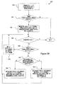
電圧コントラストテスト構造の特定のタイプにおいて、欠陥位置は、サーチタイムを最小にするサーチを実行することによって決定されえる。本発明のある実施形態において、欠陥は、例えばテスト構造の全体の長さにわたって連続的に走査するのではなく、テスト構造のさまざまな位置へと段階的に移動する(stepping)ことによって位置特定されえる。それぞれのステップ位置において、テスト構造は電子ビームによって走査される(例えばラスター走査される)。この「加速されたサーチ」手法は、上述の大きな導電構造を持つテスト構造に加えて、任意の適切なテスト構造上で実現されえる。そのような加速されたサーチのうちの一例は、2進探索である。もちろん、1つ以上のステップで素早く欠陥位置へ「ステップ移動する」ために任意の適切なサーチステップが利用されえる。例えば電子ビームは、所定の増分距離だけテスト構造に対して移動されえる。 In a particular type of voltage contrast test structure, the defect location can be determined by performing a search that minimizes the search time. In certain embodiments of the present invention, defects are located by stepping to various locations in the test structure, for example, rather than continuously scanning over the entire length of the test structure. Yeah. At each step position, the test structure is scanned by an electron beam (eg, raster scanned). This “accelerated search” approach can be implemented on any suitable test structure in addition to the test structure having the large conductive structure described above. One example of such an accelerated search is a binary search. Of course, any suitable search step can be used to quickly “step” to the defect location in one or more steps. For example, the electron beam can be moved relative to the test structure by a predetermined incremental distance.
図3Aは、本発明のある実施形態によるテスト構造300内の開放タイプの欠陥を位置特定する2進探索メカニズムを示す。図3Bは、本発明のある実施形態による欠陥を位置特定するプロシージャを示すフローチャートである。図3Aおよび3Bは併せて説明される。テスト構造は例えばターゲットパッド302においてグラウンドに接続される。最初に、操作352および354において帯電粒子ビームで構造を走査することによって、開放欠陥がテスト構造300に存在するかが決定される。例えばターゲットパッド302の電位が、電圧コントラスト検査中にレファレンスパッド308の電位と比較される。パッドの電位が異なるとき、開放欠陥がテスト構造300内に存在すると決定される。パッドが同じ電位を持つとき、欠陥は存在しないと決定される。
FIG. 3A illustrates a binary search mechanism for locating open-type defects in a
テスト構造に欠陥が存在しないと決定されるとき、プロシージャ350は終了する。欠陥が存在すると発見されるとき、帯電粒子ビームは、操作356において開放欠陥を走査するために、構造の第1部分へと構造に対して段階的に移動する。例えばテスト構造それ自身に明から暗への輝度遷移点が存在すると決定され、この点は開放欠陥の位置を示す。図3Aの図示された実施形態において、欠陥についての2進探索は、まずx方向に沿って実行される。テスト構造は上部に沿って走査されるが、テスト構造の任意の部分がサーチ中に走査されえる。電子ビームは、試料に対して位置「1」に動かされ、この位置はx方向に沿ってテスト構造300の中間にある。それから開放欠陥が見つかったかが操作358において決定される。示された実施形態において、テスト構造そのものの中に遷移点が見つかったを決定することによって、欠陥が見つかったかが決定される。もし欠陥が見つかっているなら、プロシージャは終了する。
When it is determined that there are no defects in the test structure, the
もし欠陥が見つからなかったなら、操作360において、明暗の間の輝度遷移が、前の走査および現在の走査の間で走査方向において起こっていないかが決定される。この決定は、「走査方向」内の遷移点が見つかったかに基づいており、テスト構造そのものの中に遷移点が見つかったかどうかに基づかない。例えばテスト構造は、x方向に沿って暗い部分のすぐ後に明るい部分を含みえるが、テスト構造それ自身の中の遷移点はまだ見つかっていない。
If no defect is found, it is determined at
もし走査方向内の遷移点がまだ見つかっていないなら、それから操作362において、前の走査および現在の走査の間のテスト構造中の遷移が存在するかが決定される。例えば、ターゲットパッド302および現在の走査位置1の間の遷移が存在するかが決定される。もしターゲットパッド302および位置1の間に遷移が存在すると決定されるなら、それから欠陥がサーチ位置1よりも左、つまり「後方」にあるかが決定される。言い換えれば、欠陥は前の走査(例えばパッド302)および現在の走査(例えば位置1)の間に存在すると決定される。帯電粒子ビームはそれから、現在の走査の「後方」のテスト構造の第2部分へとステップ移動され、この部分が今度は操作364において開放欠陥がないか走査される。そうでなければ、帯電粒子ビームはそれから現在の走査の「前方」のテスト構造の第2部分へステップ移動され、この部分が今度は操作366において開放欠陥がないか走査される。
If a transition point in the scan direction has not yet been found, then in
「後方」および「前方」という語は、ここでは現在のステッピング方向に対しての位置として言及される。例えば、もしビームがテストパッド302から位置1へ+x方向にステップ移動されたなら、ビームは、−x方向に移動するとき、位置1の「後方」の位置へ動くことになる。対照的にビームは、+x方向に移動するとき、位置1の「前方」の位置へ移動することになり、これはビームをパッド302から位置1へと移動させることによって規定される現在のステッピング方向と同じ方向である。
The terms “backward” and “frontward” are referred to herein as positions relative to the current stepping direction. For example, if the beam is stepped from the
遷移は位置1およびターゲットパッドの間では起こっていないので、電子ビームはそれからテスト構造に対して、位置1およびテスト構造の最右端の間の中間である位置2に移動する(操作364)。プロシージャはそれから欠陥が見つかったかを決定するために、操作358を繰り返す。この例では、欠陥が見つからなかったと決定される。それから、走査方向の遷移点は操作360では見つかっていないと決定される。それから遷移が現在の走査および前の走査の間にあると操作362で決定される。示されるように輝度レベルの遷移は、位置1および2の間で起こった。電子ビームはそれから、試料に対して、位置3へ移動し、この位置3は、位置1および2の間の中間であり、位置3において開放欠陥が走査される(操作364)。位置3においては欠陥が見つからないので、遷移は位置3および1の間にある(すなわち前の走査および現在の走査の間ではない)と決定され、電子ビームはそれから位置4へと移動し、この位置4は、位置3より左、つまり位置3の「前方」にあり、位置3および1の間の中間である(操作362)。x方向における遷移も位置4において見つけられる。
Since the transition does not occur between position 1 and the target pad, the electron beam then moves relative to the test structure to
輝度遷移が第1方向において見つかった後、電子ビームはそれからテスト構造に対して2進探索でy方向に沿って移動され、欠陥の位置を操作368で見つける。示されるように電子ビームはまずテスト構造に対して、テスト構造の長さの半分だけ下がった位置5へ移動される。輝度は位置4から5へうつるときに明および暗の間で遷移したので、次の位置6は、位置5および4の間の中間である。テスト構造そのものの中の実際の遷移点は、位置6において見つかる。それからこの遷移点が開放欠陥の位置であると決定されえる。
After the luminance transition is found in the first direction, the electron beam is then moved along the y direction in a binary search with respect to the test structure to find the position of the defect at
代替の実施形態において、テスト構造は、第1の向きに連続的に走査されることによって欠陥の存在を検出する。図1のテスト構造において、帯電粒子ビームは連続的に向き108で走査される。それからテスト構造の導電ストリップについて輝度レベルの交互の明暗があるかどうかが決定される。輝度パターンの交互のパターンは、欠陥が存在しないことを示す。しかし2つの隣接するストリップが同じ輝度レベルを持つとき、同じ輝度レベルを持つ隣接するストリップ群の中に欠陥が存在すると決定される。欠陥の位置はそれから、図3Aおよび3Bを参照して説明されたような向き106に沿った2進探索のようなステッピングサーチアルゴリズムを用いて決定されえる。暗から明への、またはその逆の輝度値の遷移がストリップ中に存在するとき、開放欠陥の位置が見つかる。物理的短絡が2つのストリップ間で見つかるとき、短絡欠陥が見つかる。
In an alternative embodiment, the test structure detects the presence of a defect by continuously scanning in a first orientation. In the test structure of FIG. 1, the charged particle beam is continuously scanned in
図4は、本発明の手法が実現されえる走査電子顕微鏡(SEM)システムの概略図である。図4の詳細は、例示目的で提供される。当業者には図4に示されるシステムの変化形も本発明の範囲に入ることが理解できるだろう。例えば図4は、連続的に移動するステージを持つ粒子ビームの動作を示す。しかしここで説明される試験構成および製品構成および多くの検査手法は、ステップアンドリピートモードで動作される粒子ビームを含む他の試験装置のコンテキストでも有用である。ビームに対してステージを移動させる代わりに、電磁レンズで視野を屈折させることによってビームが移動されてもよい。あるいはビームカラムがステージに対して移動されてもよい。 FIG. 4 is a schematic diagram of a scanning electron microscope (SEM) system in which the technique of the present invention can be implemented. The details of FIG. 4 are provided for illustrative purposes. Those skilled in the art will appreciate that variations on the system shown in FIG. 4 are within the scope of the present invention. For example, FIG. 4 shows the operation of a particle beam with a continuously moving stage. However, the test and product configurations and many inspection techniques described herein are also useful in the context of other test equipment that includes a particle beam operated in step-and-repeat mode. Instead of moving the stage relative to the beam, the beam may be moved by refracting the field of view with an electromagnetic lens. Alternatively, the beam column may be moved with respect to the stage.
試料1057は、粒子ビーム1020の下に自動的に固定される。粒子ビーム1020は、電子ビームのような粒子ビームでありえる。試料ハンドラ1034は、自動的に試料をステージ1024上で方向付けるよう構成されえる。ステージ1024は、x軸、y軸、およびz軸に沿った移動および回転を含む6自由度を持つよう構成されえる。ある具体的な実施形態において、ステージ1024は、x方向のステージの動きが検査される導電ラインの長手軸に垂直である軸に対応するようにX線放射インデューサ120に対してアラインされる。試料のアライメントの微調整は、自動で、またはシステム操作者の助けを得て達成されえる。試料1057の分析中のステージ1024の位置および動きは、ステージサーボ1026および干渉計1028によって制御されえる。ステージ1024がx方向に移動するとき、インデューサ1020は繰り返しy方向に行ったり来たり偏向されえる。さまざまな実施形態によれば、インデューサ1020はほぼ100kHzで前後に移動する。あるいは、ビームをラスタリングすることなくテスト構造の特定のバンドつまり領域にわたって走査するために、比較的に広いビームが使用されえる。 The sample 1057 is automatically fixed under the particle beam 1020. The particle beam 1020 can be a particle beam such as an electron beam. Sample handler 1034 may be configured to automatically direct a sample on stage 1024. Stage 1024 may be configured to have six degrees of freedom including movement and rotation along the x, y, and z axes. In one specific embodiment, the stage 1024 is aligned to the x-ray emission inducer 120 to correspond to an axis that is perpendicular to the longitudinal axis of the conductive line being examined in the x direction. Fine tuning of the sample alignment can be accomplished automatically or with the assistance of the system operator. The position and movement of stage 1024 during analysis of sample 1057 may be controlled by stage servo 1026 and interferometer 1028. When the stage 1024 moves in the x direction, the inducer 1020 can be repeatedly moved back and forth in the y direction. According to various embodiments, the inducer 1020 moves back and forth at approximately 100 kHz. Alternatively, a relatively wide beam can be used to scan across a specific band or region of the test structure without rastering the beam.
検出器1032はまた、さらなる欠陥検出能力を可能にするために粒子ビーム1020に並ぶようにアラインされえる。他の要素と共に検出器1032は、コントローラ1050を用いて制御されえる。コントローラ1050は、さまざまなプロセッサ、記憶要素、および入力および出力装置を含みえる。コントローラは、本発明の欠陥検査および位置特定を実現するよう構成されえる。コントローラはまた、試料上の座標で試料に対して電子ビームの座標を相関させるよう構成されえ、それによって例えば、決定された欠陥の位置を決定できる。ある実施形態において、コントローラは、プロセッサおよび1つ以上のメモリデバイスを持つコンピュータシステムである。 The detector 1032 can also be aligned to align with the particle beam 1020 to allow further defect detection capabilities. Detector 1032 along with other elements can be controlled using controller 1050. The controller 1050 can include various processors, storage elements, and input and output devices. The controller may be configured to implement the defect inspection and localization of the present invention. The controller can also be configured to correlate the coordinates of the electron beam with respect to the sample at coordinates on the sample, thereby determining, for example, the position of the determined defect. In certain embodiments, the controller is a computer system having a processor and one or more memory devices.
コントローラの構成にかかわらず、汎用検査操作および/またはここで説明された本発明の手法のためのデータ、プログラム命令を記憶するよう構成された1つ以上のメモリ、またはメモリモジュールが採用されえる。プログラム命令は、例えばオペレーティングシステムおよび/または1つ以上のアプリケーションの操作を制御しえる。メモリまたはメモリ群はまた、検査システムの特定の操作パラメータのための値と共に、走査された試料の画像、レファレンス画像、欠陥分類および位置データを記憶するよう構成されえる。 Regardless of the configuration of the controller, one or more memories or memory modules configured to store data, program instructions for general test operations and / or the inventive techniques described herein may be employed. Program instructions may control the operation of, for example, an operating system and / or one or more applications. The memory or group of memories may also be configured to store scanned sample images, reference images, defect classification and position data, along with values for specific operating parameters of the inspection system.
このような情報およびプログラム命令はここで説明されたシステム/方法を実現するために採用されえるので、本発明は、ここで説明されたさまざまな操作を実行するためのプログラム命令、状態情報などを含む機械読み出し可能な媒体にも関する。機械読み出し可能な媒体の例としては、これらに限定されないが、ハードディスク、フロッピーディスク(登録商標)、および磁気テープのような磁気媒体、CD−ROMディスクのような光学媒体、フロプティカルディスクのような光磁気媒体、および読み出し専用メモリ(ROM)およびランダムアクセスメモリ(RAM)のようなプログラム命令を記憶し実行するために特別に構成されるハードウェアデバイスがある。本発明はまた、電波、光ケーブル、電気ケーブルなどのような適切な媒体上で搬送される搬送波において実現されえる。プログラム命令の例としては、コンパイラによって生成される機械語、およびインタープリタを用いてコンピュータによって実行されえる高級言語を含むファイルの両方が含まれる。 Since such information and program instructions can be employed to implement the systems / methods described herein, the present invention provides program instructions, status information, etc. for performing the various operations described herein. It also relates to a machine readable medium including. Examples of machine readable media include, but are not limited to, magnetic media such as hard disks, floppy disks, and magnetic tape, optical media such as CD-ROM disks, and floppy disks. There are hardware devices that are specially configured to store and execute program instructions, such as random magneto-optical media and read only memory (ROM) and random access memory (RAM). The present invention can also be implemented in a carrier wave carried on a suitable medium such as radio waves, optical cables, electrical cables, and the like. Examples of program instructions include both machine language generated by a compiler and files containing high-level languages that can be executed by a computer using an interpreter.
前述の本発明は理解の明瞭さのためにある程度詳細に説明されてきたが、ある種の変更および改変が添付の特許請求の範囲内で実施されえることは明らかであろう。したがって説明された実施形態は、例示的であって限定的ではなく、本発明はここに挙げられた詳細に限定されるべきではなく、添付の特許請求の範囲およびその等価物の全ての範囲によって規定されるべきである。 Although the foregoing invention has been described in some detail for purposes of clarity of understanding, it will be apparent that certain changes and modifications may be practiced within the scope of the appended claims. Accordingly, the described embodiments are illustrative and not restrictive, and the invention should not be limited to the details listed herein, but by the appended claims and their full scope of equivalents. Should be specified.
Claims (15)
電圧コントラスト検査中に第1電位に帯電される複数のフローティング導電構造を有する第1サブ構造領域と、
前記電圧コントラスト検査中に第2電位に帯電される第2サブ構造領域と、
前記第2サブ構造領域に結合された所定のサイズの導電パッドとして形成された導電構造であって、前記第2サブ構造領域が、前記第1サブ構造領域よりもより遅く帯電することで、前記第2電位が前記電圧コントラスト検査中に前記第1の電位とは異なる電位となるよう、実験的またはシミュレーションによって前記所定のサイズが選択された導電構造と
を備えるテスト用半導体装置。A test semiconductor device having a test structure designed for voltage contrast inspection,
A first substructure region having a plurality of floating conductive structures charged to a first potential during a voltage contrast test ;
A second sub-structure region is charged to a second potential during said voltage contrast test,
A conductive structure formed as a conductive pad of a predetermined size coupled to the second sub-structure region, wherein the second sub-structure region is charged later than the first sub-structure region; A test semiconductor device comprising: a conductive structure having the predetermined size selected experimentally or by simulation so that a second potential is different from the first potential during the voltage contrast test .
電子ビームによる走査によって第1電位に帯電される複数のフローティング導電構造を有する第1サブ構造領域を形成すること、
前記電子ビームによる走査によって第2電位に帯電される第2サブ構造領域を形成すること、および
前記第2サブ構造領域に結合された導電パッドである導電構造を、前記第2サブ構造領域が、前記電子ビームによる走査を受けた際に前記第1サブ構造領域よりもより遅く帯電することで、前記第2電位が電圧コントラスト検査中に前記第1の電位とは異なる電位となるよう、実験的またはシミュレーションによって選択されたサイズとして形成すること
を含む製造方法。 A method of manufacturing a test semiconductor device designed for voltage contrast inspection,
Forming a first substructure region having a plurality of floating conductive structures charged to a first potential by scanning with an electron beam ;
Forming a second sub-structure region is charged to a second potential by scanning by the electron beam, and
The second substructure region is charged later than the first substructure region when the second substructure region is scanned by the electron beam when the conductive structure is a conductive pad coupled to the second substructure region. The manufacturing method includes forming the second potential as a size selected experimentally or by simulation so that the second potential is different from the first potential during the voltage contrast test .
Applications Claiming Priority (4)
| Application Number | Priority Date | Filing Date | Title |
|---|---|---|---|
| US32980401P | 2001-10-17 | 2001-10-17 | |
| US10/265,051 US6995393B2 (en) | 2000-08-25 | 2002-10-02 | Apparatus and methods for semiconductor IC failure detection |
| US10/264,625 US7067335B2 (en) | 2000-08-25 | 2002-10-02 | Apparatus and methods for semiconductor IC failure detection |
| PCT/US2002/033154 WO2003034492A2 (en) | 2001-10-17 | 2002-10-16 | Apparatus and methods for semiconductor ic failure detection |
Related Child Applications (1)
| Application Number | Title | Priority Date | Filing Date |
|---|---|---|---|
| JP2009219052A Division JP5238659B2 (en) | 2001-10-17 | 2009-09-24 | Apparatus and method for semiconductor IC defect detection |
Publications (3)
| Publication Number | Publication Date |
|---|---|
| JP2005519260A JP2005519260A (en) | 2005-06-30 |
| JP2005519260A5 JP2005519260A5 (en) | 2006-01-05 |
| JP4505225B2 true JP4505225B2 (en) | 2010-07-21 |
Family
ID=27401722
Family Applications (1)
| Application Number | Title | Priority Date | Filing Date |
|---|---|---|---|
| JP2003537118A Expired - Fee Related JP4505225B2 (en) | 2001-10-17 | 2002-10-16 | Apparatus and method for semiconductor IC defect detection |
Country Status (2)
| Country | Link |
|---|---|
| JP (1) | JP4505225B2 (en) |
| WO (1) | WO2003034492A2 (en) |
Families Citing this family (14)
| Publication number | Priority date | Publication date | Assignee | Title |
|---|---|---|---|---|
| US9799575B2 (en) | 2015-12-16 | 2017-10-24 | Pdf Solutions, Inc. | Integrated circuit containing DOEs of NCEM-enabled fill cells |
| US9805994B1 (en) | 2015-02-03 | 2017-10-31 | Pdf Solutions, Inc. | Mesh-style NCEM pads, and process for making semiconductor dies, chips, and wafers using in-line measurements from such pads |
| US10199283B1 (en) | 2015-02-03 | 2019-02-05 | Pdf Solutions, Inc. | Method for processing a semiconductor wager using non-contact electrical measurements indicative of a resistance through a stitch, where such measurements are obtained by scanning a pad comprised of at least three parallel conductive stripes using a moving stage with beam deflection to account for motion of the stage |
| US10593604B1 (en) | 2015-12-16 | 2020-03-17 | Pdf Solutions, Inc. | Process for making semiconductor dies, chips, and wafers using in-line measurements obtained from DOEs of NCEM-enabled fill cells |
| US10978438B1 (en) | 2015-12-16 | 2021-04-13 | Pdf Solutions, Inc. | IC with test structures and E-beam pads embedded within a contiguous standard cell area |
| US9905553B1 (en) | 2016-04-04 | 2018-02-27 | Pdf Solutions, Inc. | Integrated circuit containing standard logic cells and library-compatible, NCEM-enabled fill cells, including at least via-open-configured, AACNT-short-configured, GATECNT-short-configured, and metal-short-configured, NCEM-enabled fill cells |
| US9929063B1 (en) | 2016-04-04 | 2018-03-27 | Pdf Solutions, Inc. | Process for making an integrated circuit that includes NCEM-Enabled, tip-to-side gap-configured fill cells, with NCEM pads formed from at least three conductive stripes positioned between adjacent gates |
| US9653446B1 (en) | 2016-04-04 | 2017-05-16 | Pdf Solutions, Inc. | Integrated circuit containing standard logic cells and library-compatible, NCEM-enabled fill cells, including at least via-open-configured, AACNT-short-configured, TS-short-configured, and AA-short-configured, NCEM-enabled fill cells |
| US9748153B1 (en) | 2017-03-29 | 2017-08-29 | Pdf Solutions, Inc. | Process for making and using a semiconductor wafer containing first and second does of standard cell compatible, NCEM-enabled fill cells, with the first DOE including side-to-side short configured fill cells, and the second DOE including tip-to-side short configure |
| US9773774B1 (en) | 2017-03-30 | 2017-09-26 | Pdf Solutions, Inc. | Process for making and using a semiconductor wafer containing first and second DOEs of standard cell compatible, NCEM-enabled fill cells, with the first DOE including chamfer short configured fill cells, and the second DOE including corner short configured fill cells |
| US9768083B1 (en) | 2017-06-27 | 2017-09-19 | Pdf Solutions, Inc. | Process for making and using a semiconductor wafer containing first and second DOEs of standard cell compatible, NCEM-enabled fill cells, with the first DOE including merged-via open configured fill cells, and the second DOE including snake open configured fill cells |
| US9786649B1 (en) | 2017-06-27 | 2017-10-10 | Pdf Solutions, Inc. | Process for making and using a semiconductor wafer containing first and second DOEs of standard cell compatible, NCEM-enabled fill cells, with the first DOE including via open configured fill cells, and the second DOE including stitch open configured fill cells |
| US10096530B1 (en) | 2017-06-28 | 2018-10-09 | Pdf Solutions, Inc. | Process for making and using a semiconductor wafer containing first and second DOEs of standard cell compatible, NCEM-enabled fill cells, with the first DOE including merged-via open configured fill cells, and the second DOE including stitch open configured fill cells |
| US9865583B1 (en) | 2017-06-28 | 2018-01-09 | Pdf Solutions, Inc. | Process for making and using a semiconductor wafer containing first and second DOEs of standard cell compatible, NCEM-enabled fill cells, with the first DOE including snake open configured fill cells, and the second DOE including stitch open configured fill cells |
Family Cites Families (5)
| Publication number | Priority date | Publication date | Assignee | Title |
|---|---|---|---|---|
| JPH05144901A (en) * | 1991-11-21 | 1993-06-11 | Oki Electric Ind Co Ltd | Detection of defective point of device having fine pattern |
| JP3356056B2 (en) * | 1998-05-15 | 2002-12-09 | 日本電気株式会社 | Wiring fault detecting circuit, wiring fault detecting semiconductor wafer, and wiring fault detecting method using the same |
| US6268717B1 (en) * | 1999-03-04 | 2001-07-31 | Advanced Micro Devices, Inc. | Semiconductor test structure with intentional partial defects and method of use |
| US6452412B1 (en) * | 1999-03-04 | 2002-09-17 | Advanced Micro Devices, Inc. | Drop-in test structure and methodology for characterizing an integrated circuit process flow and topography |
| JP3708763B2 (en) * | 1999-08-31 | 2005-10-19 | 株式会社東芝 | Defect detection method |
-
2002
- 2002-10-16 JP JP2003537118A patent/JP4505225B2/en not_active Expired - Fee Related
- 2002-10-16 WO PCT/US2002/033154 patent/WO2003034492A2/en active Application Filing
Also Published As
| Publication number | Publication date |
|---|---|
| WO2003034492A8 (en) | 2003-11-13 |
| JP2005519260A (en) | 2005-06-30 |
| WO2003034492A2 (en) | 2003-04-24 |
| WO2003034492A3 (en) | 2003-07-10 |
Similar Documents
| Publication | Publication Date | Title |
|---|---|---|
| US6995393B2 (en) | Apparatus and methods for semiconductor IC failure detection | |
| US7067335B2 (en) | Apparatus and methods for semiconductor IC failure detection | |
| US7198963B2 (en) | Methodologies for efficient inspection of test structures using electron beam scanning and step and repeat systems | |
| US6861666B1 (en) | Apparatus and methods for determining and localization of failures in test structures using voltage contrast | |
| JP4657394B2 (en) | Method and apparatus for detecting defects in a wafer | |
| JP4505225B2 (en) | Apparatus and method for semiconductor IC defect detection | |
| KR102445535B1 (en) | Systems and Methods for Area-Adaptive Fault Detection | |
| US6948141B1 (en) | Apparatus and methods for determining critical area of semiconductor design data | |
| US9793090B2 (en) | E-beam inspection apparatus and method of using the same on various integrated circuit chips | |
| US6855568B2 (en) | Apparatus and methods for monitoring self-aligned contact arrays using voltage contrast inspection | |
| US6566885B1 (en) | Multiple directional scans of test structures on semiconductor integrated circuits | |
| KR100775437B1 (en) | Pattern inspection device and method | |
| US7656170B2 (en) | Multiple directional scans of test structures on semiconductor integrated circuits | |
| US7280945B1 (en) | Apparatus and methods for detection of systematic defects | |
| US6642726B2 (en) | Apparatus and methods for reliable and efficient detection of voltage contrast defects | |
| US20030097228A1 (en) | Apparatus and methods for managing reliability of semiconductor devices | |
| US6732002B1 (en) | Apparatus and methods for predicting multiple product chip yields through critical area matching | |
| US7733099B2 (en) | Monitoring pattern for detecting a defect in a semiconductor device and method for detecting a defect | |
| Satya | Microelectronic test structures for rapid automated contactless inline defect inspection | |
| JP2005519260A5 (en) | ||
| JP5238659B2 (en) | Apparatus and method for semiconductor IC defect detection | |
| US6906538B2 (en) | Alternating pulse dual-beam apparatus, methods and systems for voltage contrast behavior assessment of microcircuits | |
| US6774648B1 (en) | Apparatus and methods for optically detecting defects in voltage contrast test structures |
Legal Events
| Date | Code | Title | Description |
|---|---|---|---|
| A621 | Written request for application examination |
Free format text: JAPANESE INTERMEDIATE CODE: A621 Effective date: 20051014 |
|
| A521 | Request for written amendment filed |
Free format text: JAPANESE INTERMEDIATE CODE: A523 Effective date: 20051017 |
|
| A131 | Notification of reasons for refusal |
Free format text: JAPANESE INTERMEDIATE CODE: A131 Effective date: 20090324 |
|
| A601 | Written request for extension of time |
Free format text: JAPANESE INTERMEDIATE CODE: A601 Effective date: 20090623 |
|
| A602 | Written permission of extension of time |
Free format text: JAPANESE INTERMEDIATE CODE: A602 Effective date: 20090630 |
|
| A521 | Request for written amendment filed |
Free format text: JAPANESE INTERMEDIATE CODE: A523 Effective date: 20090924 |
|
| TRDD | Decision of grant or rejection written | ||
| A01 | Written decision to grant a patent or to grant a registration (utility model) |
Free format text: JAPANESE INTERMEDIATE CODE: A01 Effective date: 20100330 |
|
| A01 | Written decision to grant a patent or to grant a registration (utility model) |
Free format text: JAPANESE INTERMEDIATE CODE: A01 |
|
| A61 | First payment of annual fees (during grant procedure) |
Free format text: JAPANESE INTERMEDIATE CODE: A61 Effective date: 20100426 |
|
| R150 | Certificate of patent or registration of utility model |
Ref document number: 4505225 Country of ref document: JP Free format text: JAPANESE INTERMEDIATE CODE: R150 Free format text: JAPANESE INTERMEDIATE CODE: R150 |
|
| FPAY | Renewal fee payment (event date is renewal date of database) |
Free format text: PAYMENT UNTIL: 20130430 Year of fee payment: 3 |
|
| FPAY | Renewal fee payment (event date is renewal date of database) |
Free format text: PAYMENT UNTIL: 20130430 Year of fee payment: 3 |
|
| FPAY | Renewal fee payment (event date is renewal date of database) |
Free format text: PAYMENT UNTIL: 20140430 Year of fee payment: 4 |
|
| R250 | Receipt of annual fees |
Free format text: JAPANESE INTERMEDIATE CODE: R250 |
|
| R250 | Receipt of annual fees |
Free format text: JAPANESE INTERMEDIATE CODE: R250 |
|
| R250 | Receipt of annual fees |
Free format text: JAPANESE INTERMEDIATE CODE: R250 |
|
| R250 | Receipt of annual fees |
Free format text: JAPANESE INTERMEDIATE CODE: R250 |
|
| R250 | Receipt of annual fees |
Free format text: JAPANESE INTERMEDIATE CODE: R250 |
|
| R250 | Receipt of annual fees |
Free format text: JAPANESE INTERMEDIATE CODE: R250 |
|
| R250 | Receipt of annual fees |
Free format text: JAPANESE INTERMEDIATE CODE: R250 |
|
| R250 | Receipt of annual fees |
Free format text: JAPANESE INTERMEDIATE CODE: R250 |
|
| R250 | Receipt of annual fees |
Free format text: JAPANESE INTERMEDIATE CODE: R250 |
|
| LAPS | Cancellation because of no payment of annual fees |