JP4500547B2 - Detection of molecular probes immobilized in the reactive zone of the sensor - Google Patents
Detection of molecular probes immobilized in the reactive zone of the sensor Download PDFInfo
- Publication number
- JP4500547B2 JP4500547B2 JP2003562625A JP2003562625A JP4500547B2 JP 4500547 B2 JP4500547 B2 JP 4500547B2 JP 2003562625 A JP2003562625 A JP 2003562625A JP 2003562625 A JP2003562625 A JP 2003562625A JP 4500547 B2 JP4500547 B2 JP 4500547B2
- Authority
- JP
- Japan
- Prior art keywords
- transistors
- zone
- molecular probe
- dna
- source
- Prior art date
- Legal status (The legal status is an assumption and is not a legal conclusion. Google has not performed a legal analysis and makes no representation as to the accuracy of the status listed.)
- Expired - Lifetime
Links
Images


Classifications
-
- C—CHEMISTRY; METALLURGY
- C12—BIOCHEMISTRY; BEER; SPIRITS; WINE; VINEGAR; MICROBIOLOGY; ENZYMOLOGY; MUTATION OR GENETIC ENGINEERING
- C12Q—MEASURING OR TESTING PROCESSES INVOLVING ENZYMES, NUCLEIC ACIDS OR MICROORGANISMS; COMPOSITIONS OR TEST PAPERS THEREFOR; PROCESSES OF PREPARING SUCH COMPOSITIONS; CONDITION-RESPONSIVE CONTROL IN MICROBIOLOGICAL OR ENZYMOLOGICAL PROCESSES
- C12Q1/00—Measuring or testing processes involving enzymes, nucleic acids or microorganisms; Compositions therefor; Processes of preparing such compositions
- C12Q1/001—Enzyme electrodes
- C12Q1/002—Electrode membranes
- C12Q1/003—Functionalisation
Abstract
Description
本発明は、センサーのゾーンに固定された分子プローブの代表的な少なくとも1つのパラメータを検出するための方法に関する。 The present invention relates to a method for detecting at least one representative parameter of a molecular probe immobilized in a zone of a sensor.
電界効果形トランジスタを用いてDNA配列のハイブリダイゼーションを検出するための方法は、E. SOUTEYRANDらにより“Direct Detection of the hybridization of synthetic Homo-Oligomer DNA Sequences by Field Effect”の題名で、J. Phys. Chem. B1997、101、第2980〜2985頁に1997年に出版されている、論文に記載されているように、既に知られている。このタイプの使用に用いられ得るISFET (イオン感受性電界効果形トランジスタ)タイプのトランジスタは、IEEE Transactions on Biomedical Engineering 第BME-19巻 - 第5号、September 1972、第342〜351頁に出版されているPiet BERGVELDによる“Development, Operation and Application of the ISFET as a Tool for Electrophysiology”の論文に記載されている。 A method for detecting hybridization of DNA sequences using a field effect transistor is the title of “Direct Detection of the hybridization of synthetic Homo-Oligomer DNA Sequences by Field Effect” by E. SOUTEYRAND et al., J. Phys. Chem. B1997, 101, pages 2980-2985, already known as described in a paper published in 1997. ISFET (Ion Sensitive Field Effect Transistor) type transistors that can be used for this type of use are published in IEEE Transactions on Biomedical Engineering Vol. BME-19-No. 5, September 1972, pages 342-351 It is described in the paper “Development, Operation and Application of the ISFET as a Tool for Electrophysiology” by Piet BERGVELD.
このようなトランジスタ構造の製作の記載は、“Extracellular Resistance in Cell Adhesion Measured with a Transistor Probe”の題名で、Langmuir 2000、16、第3517〜3521頁に出版されている、V. KIESSLINGらによる論文に見出すことができる。最後に、サーフェスプレパレーション法は、"Silanized nucleid acids: a general platform for DNA immobilization"の題名で、Nucleic Acid Research 2000、第28巻、第14号、第i〜vi頁に出版されている、A. KUMAR らの論文に記載されている。 A description of the fabrication of such a transistor structure can be found in a paper by V. KIESSLING et al., Published in Langmuir 2000, 16, pp. 3517-3521, entitled “Extracellular Resistance in Cell Adhesion Measured with a Transistor Probe”. Can be found. Finally, the surface preparation method is titled “Silanized nucleid acids: a general platform for DNA immobilization” and is published in Nucleic Acid Research 2000, Vol. 28, No. 14, pp. I-vi. It is described in a paper by KUMAR et al.
本発明の関係において、表面に分子プローブを固定するための2つの方法を特に用いることができる。第一は、例えば“Light-directed, spatially addressable parallel chemical synthesis”の題名で、Science 251、第767〜773頁(1991)に出版されている、S.P.A. Fodorらによる論文に記載されているように、固相上への直接の合成からなる。第二は、希釈液を用いる分子の固定である。 In the context of the present invention, two methods for immobilizing molecular probes on the surface can be used in particular. The first is, for example, the title “Light-directed, spatially addressable parallel chemical synthesis”, as described in a paper by SPA Fodor et al. Published in Science 251, pages 767-773 (1991), It consists of direct synthesis on the solid phase. The second is immobilization of molecules using a diluent.
複数の反応性ゾーンを含むセンサー、例えばDNAチップまたはタンパク質チップの場合、分子プローブが効率的に固定されたゾーンを、比較的迅速な様式で、容易に調節する技術は、現在、入手できない。 In the case of sensors that include multiple reactive zones, such as DNA chips or protein chips, no technology is currently available to easily adjust a zone in which molecular probes are efficiently immobilized in a relatively fast manner.
したがって、本発明の目的は、特に、実際問題として頻繁に遭遇するかなりの実験的変動によりおこる問題を少なくとも部分的に軽減することを可能にするように、特に分子プローブの局部沈積(local deposition)および局部固定を調節する目的のための、センサーの少なくとも1つのゾーンに固定された分子プローブの代表的な少なくとも1つのパラメータを検出する方法である。 The object of the invention is therefore in particular the local deposition of molecular probes, in particular so as to make it possible to at least partially alleviate the problems caused by the considerable experimental variation frequently encountered as a practical problem. And a method for detecting at least one representative parameter of a molecular probe immobilized in at least one zone of the sensor for the purpose of adjusting local fixation.
したがって本発明は、センサーが、電界効果形トランジスタのネットワークからなり、各トランジスタはソース領域、ドレイン領域、およびその上で分子プローブの代表的なパラメータが検出されるべき反応性ゾーンを形成するゲート領域を有し、かつ次の工程:
a) 分子プローブを固定するために、該ゾーンの一部を該プローブと接触させ、
b) 分子プローブと接触された少なくともこれらのゾーンを電解質溶液中に浸し、
c) 例えば第一群のこれらのトランジスタ、バイアスをかけられているドレインおよびソースに、ゲートおよびソース間の所定の電圧、例えば一定電圧を、または代わりに所定のドレイン電流、例えば一定電流を印加することにより、分子プローブと接触させたゾーンに対応する第一群のトランジスタ中の少なくとも2つに特徴的なドレイン電流/ソース−ゲート電圧/ソース−ドレイン電圧の少なくとも1点を測定し、2つの異なるゾーンについて得られた測定の少なくとも2つの間の比較により、少なくとも1つの該代表的パラメータをそこから導出する
ことを含むことを特徴とする、センサーの少なくとも1つの反応性ゾーンに固定された分子プローブの代表的な少なくとも1つのパラメータを検出する方法に関する。
Accordingly, the present invention provides a sensor comprising a network of field effect transistors, each transistor forming a source region, a drain region, and a gate region on which a typical parameter of a molecular probe is to be detected. And having the following steps:
a ) to immobilize a molecular probe, a part of the zone is brought into contact with the probe;
b ) soak at least these zones in contact with the molecular probe in the electrolyte solution;
c ) Applying a predetermined voltage between the gate and source, for example a constant voltage, or alternatively a predetermined drain current, for example a constant current, for example to the first group of these transistors, the drain and source being biased it makes at least characteristic drain current / source into two in the transistor of the first group corresponding to the zone in contact with molecular probes - gate voltage / source - measuring at least one point of the drain voltage, the two Molecule immobilized in at least one reactive zone of the sensor, characterized in that it comprises deriving at least one said representative parameter therefrom by comparison between at least two measurements obtained for different zones The present invention relates to a method for detecting at least one representative parameter of a probe.
該比較は、差動測定を用いて行われることが好ましい。代表的パラメータは、分子プローブの固定の検出であり得る。
工程a)およびb)の間に、リンスを行うことが想定できる。
The comparison is preferably performed using differential measurements. An exemplary parameter may be detection of molecular probe immobilization.
It can be assumed that a rinsing is performed during steps a) and b).
特定の実施形態によると、本方法は、次の工程:
a1) リンスを行い、
a2) 分子プローブと特異的に相互作用し得る、例えば分子プローブがDNAである場合に、それらとハイブリダイズし得る標的分子を含む溶液を添加し、任意にその後リンスを行う
を、a)の後であってb)の前に含むことを特徴とする。
According to a particular embodiment, the method comprises the following steps:
a1) Rinse and
a2) If the molecular probe is DNA, which can interact specifically with the molecular probe, for example, add a solution containing the target molecule that can hybridize to it, and optionally perform a subsequent rinse, after a) And is included before b).
その他の特定の実施形態によると、本方法は、次の工程:
d) 分子プローブと特異的に相互作用し得る、例えば分子プローブがDNAである場合に、ハイブリダイズし得る標的分子を含む電解質溶液を添加し、
e) 少なくとも1つの該代表的パラメータを比較により得るように、例えば第二群のこれらのトランジスタのゲートおよびソース、バイアスをかけられたドレインおよびソースの間に電圧、例えば一定電圧を、または第二のこれらのトランジスタのソースに所定の電流、例えば一定電流を印加することにより、分子プローブおよび標的分子と接触させたゾーンに対応する第二群のトランジスタの少なくとも2つに特徴的なドレイン電流/ソース−ゲート電圧/ソース−ドレイン電圧の少なくとも1点を測定する
を、cの後に含むことを特徴とする。
According to another particular embodiment, the method comprises the following steps:
d) Add an electrolyte solution containing a target molecule that can specifically interact with the molecular probe, for example when the molecular probe is DNA,
e) a voltage, for example a constant voltage, or a second voltage, for example, between the gate and source of these transistors in the second group, the biased drain and source, so as to obtain at least one representative parameter by comparison The drain current / source characteristic of at least two of the second group of transistors corresponding to the zone in contact with the molecular probe and the target molecule by applying a predetermined current, eg a constant current, to the source of these transistors - gate voltage / source - the measuring of at least one point of the drain voltage, characterized in that it comprises after c.
本方法は、時間に関して間隔をあけている、特性の少なくとも1点の測定の複数を用いることができる。これは、空間的および時間に関する2重の比較ができる測定値を得ることを可能にする。 The method can use a plurality of measurements of at least one point of the characteristic that are spaced in time. This makes it possible to obtain measurements that allow a double comparison in terms of space and time.
第一の変形によると、特に差動測定による比較は、分子プローブに接触させた後に電解質溶液に浸されたゾーンに対応する少なくとも2つのトランジスタの間で行われる。 According to a first variant, the comparison, in particular by differential measurement, is performed between at least two transistors corresponding to the zones immersed in the electrolyte solution after being brought into contact with the molecular probe.
好ましい第二の変形によると、特に差動測定によるこの比較は、分子プローブに接触させた後に該電解質溶液に浸されたゾーンに対応する少なくとも1つのトランジスタ、および予め分子プローブに接触させずに該電解質溶液に浸されたゾーンに対応する少なくとも1つのトランジスタの間で行われる。
分子プローブは、例えばDNA、RNAまたはタンパク質分子である。
According to a preferred second variant, this comparison, in particular by differential measurement, shows that at least one transistor corresponding to the zone immersed in the electrolyte solution after contact with the molecular probe, and without contact with the molecular probe in advance. This is done between at least one transistor corresponding to a zone immersed in the electrolyte solution.
Molecular probes are for example DNA, RNA or protein molecules.
本発明による方法は、通常の、蛍光による分子の相互作用の検出に影響を及ぼさない。 The method according to the invention does not affect the normal detection of molecular interactions by fluorescence.
本発明のその他の特徴および利点は:
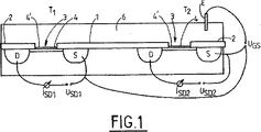
−図1は、トランジスタの1次元または2次元のネットワークにより組織化されたトランジスタの複数を含む、検出チップの2つの電界効果形トランジスタを表し;
−図2は、上から見た、検出チップ、およびそれぞれ電界効果形トランジスタに対応する反応性ゾーンの配置の詳細を表し;
Other features and advantages of the present invention are:
FIG. 1 represents two field effect transistors of a detection chip, comprising a plurality of transistors organized by a one-dimensional or two-dimensional network of transistors;
FIG. 2 represents the details of the arrangement of the detection chip and the reactive zones corresponding to the field effect transistors, respectively, viewed from above;
−図3は、1次元または2次元のネットワークの伝送(transmissions)の電気的ドレイン接続を図解し、図4は、種々の電気的ドレイン接続の抵抗を表し、カーブAは計算値を、そしてカーブBは測定値を表し、カーブ間の差は、ほとんどが、一定のチャネル抵抗によるものであり;
−図5は、選択された反応性ゾーンに溶液を沈積させるための装置を表し;
−図6は、ドレイン電流ISDの変動による、USGおよびUSD一定での、シラン処理されたDNAおよびポリ-L-リシンの存在の検出を図解し;
-Figure 3 illustrates the electrical drain connections for one or two dimensional network transmissions, Figure 4 represents the resistance of the various electrical drain connections, curve A represents the calculated value, and curve B represents the measured value, the difference between the curves is mostly due to constant channel resistance;
-Figure 5 represents an apparatus for depositing a solution in a selected reactive zone;
- Figure 6 illustrates by variation of the drain current I SD, with U SG and U SD constant, the silanized DNA and poly -L- detecting the presence of lysine;
−図7は、電圧USGの変動の検出による、ISDおよびUSD一定での、シラン処理されたDNAおよびポリ-L-リシンの存在の検出を図解し;
−図8A〜8Cは、種々の実験条件下で行った実験の結果を表し;
−図9A〜9Dは、DNAの電子検出を表し;
−そして、図10Aおよび10Bは、マイクロ流体チャネルの使用を図解する
である添付の図とともに、以下の本明細書の記載を読めばより明確になるであろう。
- Figure 7 is illustrated by the detection of the variation of the voltage U SG, with I SD and U SD constant, the silanized DNA and poly -L- detecting the presence of lysine;
-Figures 8A-8C represent the results of experiments conducted under various experimental conditions;
-Figures 9A-9D represent the electronic detection of DNA;
-Figures 10A and 10B will become clearer upon reading the description herein below, along with the accompanying figures that illustrate the use of microfluidic channels.
図1〜3は、シリコン基板上に電界効果形トランジスタのネットワークを有するセンサーを図解している。図1に断面図として表されるトランジスタT1またはT2は、それぞれが電気的接点を示し、かつそれぞれ絶縁層1および2、例えばSiO2熱酸化物が上に載せられているソース領域Sおよびドレイン領域Dとともに与えられる。ソースSおよびドレインDの間の反応性領域3は、トランジスタのゲート領域Gを形成し、そして薄い絶縁層4、例えば熱SiO2の層を有する。この反応性領域上に酸化物を有さないことも可能である。次いで、反応性表面は、絶縁材料が取り除かれた基板の4'部分により区切られる。
FIGS. 1-3 illustrate a sensor having a network of field effect transistors on a silicon substrate. Transistors T 1 or T 2 represented in cross-section in FIG. 1 each represent an electrical contact, and a source region S and an
分子プローブ、例えば一本鎖DNA分子を、反応性表面4または4'の少なくとも一部に、周知の方法により固定する。DNAについては、デプレッションn-チャネル電界効果形トランジスタ(これに対する電荷担体は、より可動である電子であり、よって感度が増大)を、負のゲートバイアスとともに(すなわち、電解質は半導体に関して負にバイアスされている)用いることが好ましく、該DNAは負に荷電されている(中性pHの電解質について)。
A molecular probe, such as a single-stranded DNA molecule, is immobilized on at least a part of the
ソースSおよびドレインDの間のソース−ドレイン電圧USD (T1についてUSD1、およびT2についてUSD2)、ならびに電解質6およびソースSの間のゲート−ソース電圧UGS (例えば単独のAg/AgCl電極Eによる)の印加は、Si/SiO2界面、または各抵抗体のSi/電解質界面における電荷担体の2次元ガスを誘導する。ドレイン電流IDは、各トランジスタについて、SiO2/電解質またはSi/電解質界面における電荷に実質的に依存するそれから得られる。ソースSおよびドレインDの間のチャネルに面するこの界面を、反応性表面という。
Source-drain voltage U SD between source S and drain D (U SD1 for T 1 and U SD2 for T 2 ), and gate-source voltage U GS between
電流IDは、反応性表面4または4'への分子プローブ、例えばDNA分子の固定に依存する。
The current ID depends on the immobilization of a molecular probe, such as a DNA molecule, on the
図2および3に示すように、電界効果形トランジスタタイプのn個の構造は、絶縁体(SiO2またはその他)で被覆され、かつソース10およびドレイン(D1、・・・Dn)の電気的接続により適切な接続(金属化、または好ましくはドープされた導電性領域)が提供されたシリコン基板中に集積される。標準のMOSトランジスタ構造とは異なり、金属ゲート電極は存在しない。これは、"ISFET" (Ion Sensitive Field Effect Transistor、イオン感受性電界効果形トランジスタ)タイプの構造に一致する。より高い感度を与えるSOI (silicon-on-isolator、シリコンオンアイソレーター)タイプの基板が好ましく用いられる。
As shown in FIGS. 2 and 3, n field-effect transistor type structures are covered with an insulator (SiO 2 or other) and the electrical properties of the
種々の構造が互いに横に近接しており、そしてそれらの反応性表面は、同じ測定溶液に接触する。現行のマイクロエレクトロニクスの典型的な横の寸法は、1μm未満である。本発明において用いられるようなDNAチップ技術においては、横の寸法は、固相上への直接合成については5〜10μmであり、希釈液を用いる分子の固定の場合は50〜100μmである。 Various structures are laterally adjacent to each other and their reactive surfaces are in contact with the same measurement solution. Typical lateral dimensions of current microelectronics are less than 1 μm. In the DNA chip technology as used in the present invention, the horizontal dimension is 5-10 μm for direct synthesis on a solid phase and 50-100 μm for the immobilization of molecules using a diluent.
本発明の並列の測定配置においては、固定化された分子プローブの種々のタイプのいくつかのプロットが同じ測定溶液に接触しており、そして少なくとも1つのトランジスタ構造が各プロットより下に位置する。プロット当たりいくつかのトランジスタの使用は、上記の寸法の観点から可能であり、そして検出における重複を可能にする。 In the parallel measurement arrangement of the present invention, several plots of different types of immobilized molecular probes are in contact with the same measurement solution, and at least one transistor structure is located below each plot. The use of several transistors per plot is possible in terms of the above dimensions and allows overlap in detection.
電極E (例えばAg/AgCl)を用いて、それが被覆するシリコン構造に関する測定溶液6 (電解質)の電位を設定し、そしてセンサー(トランジスタ)の動作点を設定する。ある場合においては、電解質6の電位は0に等しいことが可能である。センサーを浸す測定溶液6は、充分な導電率を与え、かつ反応性表面のより広い遮へいを起こさない濃度のイオンを含む。これは、中性pHを有するのが好ましい。
The electrode E (eg Ag / AgCl) is used to set the potential of the measuring solution 6 (electrolyte) with respect to the silicon structure that it covers and the operating point of the sensor (transistor). In some cases, the potential of the
分子認識(molecular recognitions)を検出するための方法は、比較、特に差動比較によるアプローチに基づく。測定は、並列のいくつかのトランジスタ構造を用いて行われる。測定は、グラフトされた(grafted)分子の種々のタイプに関して差異に基づくものであっ
てよく、そして分子のタイプ当たりいくつかのトランジスタを任意に含むことができる。分子認識(および/またはこの反応中の進展)を明らかにする反応の前/後のシグナルを比較することも可能である。
The method for detecting molecular recognitions is based on a comparison, in particular a differential comparison approach. Measurements are made using several transistor structures in parallel. The measurement may be based on differences for various types of grafted molecules and may optionally include several transistors per type of molecule. It is also possible to compare the signals before / after the reaction revealing molecular recognition (and / or progress during this reaction).
本発明の方法は、pHおよびイオン強度に対する個別のセンサーの感度に関連する問題点、および1つの個別のトランジスタからその他へのばらつきに関する問題点(これは、トランジスタ構造およびプローブの固定の質を含む)を回避することを可能にする。 The method of the present invention has problems related to the sensitivity of individual sensors to pH and ionic strength, and problems related to variations from one individual transistor to the other (this includes the quality of the transistor structure and probe immobilization. ) Can be avoided.
好ましい実施形態による本方法は、次の工程:
a) 分子プローブの固定を準備するための絶縁表面全体の均質な処理;
b) 個別の反応性表面の少なくとも一部への分子プローブの種々のタイプの局所グラフト化;
c) 均質なリンス;
d) 電子測定:測定電解質を添加し、電極を浸し、そしてトランジスタを測定し(例えばUSDおよびUSGの関数としての特性IDの1以上の点)、得られた結果をトランジスタにより比較する;
e) 均質なリンス;
f) そして、任意の、電解質の存在下での標的分子の溶液の添加、および認識反応;
g) 均質なリンス;
h) (d)のような電子測定
を用いる。
The method according to a preferred embodiment comprises the following steps:
a) Homogeneous treatment of the entire insulating surface to prepare the molecular probe fixation;
b) various types of local grafting of molecular probes onto at least a part of individual reactive surfaces;
c) Homogeneous rinsing;
d) Electronic measurement: adding measurement electrolyte, immersing the electrode and measuring the transistor (eg one or more points of characteristic ID as a function of USD and USG ) and comparing the results obtained with the transistor ;
e) Homogeneous rinse;
f) and optional addition of a solution of the target molecule in the presence of an electrolyte and recognition reaction;
g) homogeneous rinsing;
h) Use electronic measurements such as (d).
工程f〜hを用いる場合、cおよびdを省略すること、すなわちただ1度だけ電子測定を行うことが可能である。 When using steps f to h, it is possible to omit c and d , ie to make an electronic measurement only once.
分子プローブと接触させていないいくつかのトランジスタ(または、でなければ単独のトランジスタ)は、コントロールになり得る。これらの特性は、例えば全てのトランジスタを浸す測定電解質の添加の後に測定する。 Some transistors (or otherwise single transistors) that are not in contact with the molecular probe can be in control. These properties are measured, for example, after the addition of a measurement electrolyte that immerses all transistors.
分子プローブのグラフト化は、直径約100μmの微小液滴を、市場で入手可能な金属のマイクロペンを用いてトランジスタの反応性表面上に沈積させることにより行われる。 Molecular probe grafting is performed by depositing about 100 μm diameter microdroplets onto the reactive surface of a transistor using a commercially available metal micropen.
図3に示すように、n個のトランジスタのネットワーク(例えばn = 96トランジスタ)は、n個のドレイン接続D1、D2・・・Dn、および共通のソースに等しい2の接続(図示せず)を有する。これらの接続と関連する直列抵抗Rcは、ドレインのインデックス 1・・・nに依存する値を有する。
例えばシリコンのドーピングにより製造されるこれらの抵抗Rcの値は、無視できない。
As shown in FIG. 3, a network of n transistors (e.g., n = 96 transistors) has n drain connections D 1 , D 2 ... D n , and two connections equal to a common source (not shown). )). Series resistance R c associated with these connections has a value that depends on the
For example, the value of these resistances R c produced by doping silicon is not negligible.
この趣意において、ドレイン接続抵抗Rcは、ドープされたラインの幾何学上の長さ、および断面積から算出され、その抵抗率は既知である。算出値は、DC電圧(例えばUSD = 0.1VおよびUSG = 2 V)を印加することによるドレインインデックスの関数としての抵抗の測定値と比較する。これにより、例として図4に与えられる補正カーブを得ることが可能になる。 In this sense, the drain connection resistance R c is calculated from the geometric length of the doped line and the cross-sectional area, and its resistivity is known . The calculated value is compared to a measured value of resistance as a function of drain index by applying a DC voltage (eg, U SD = 0.1 V and U SG = 2 V). This makes it possible to obtain the correction curve given in FIG. 4 as an example.
図5に表されるような装置は、本方法を実行するのに用いることができる:プラットホーム12がテーブル10の上に設置され、該プラットホームには、テーブル11に、3つの直交方向X、YおよびZへの移動を提供するマイクロコントローラを含むコントロール装置が組み込まれている。n個のトランジスタのネットワークを組み込んだチップ15は、支持体14上に設置される。3方向X、YおよびZへの移動を提供するテーブル21を含むもう1つのプラットホーム20は、n個のトランジスタの少なくとも一部に微小液滴を沈積させるためのマイクロペン、またはピペット23を保持するアーム22を移動するのに用いられる。スクリーン19に連結されたカメラおよび/または対物レンズ17は、微小液滴の沈積を観察し、操作を制御するのを可能にする。
An apparatus as represented in FIG. 5 can be used to carry out the method: a
ドレイン電流ID測定は、例えばUSG = 1 VおよびUSD = 0.9 V、ならびにリットル当たり0.1ミリモルの濃度のKClからなる中性pHの沈積された電解質を用いて行われる。トランジスタ(p-チャネル蓄積トランジスタ)が相互に連絡されたそれらのソースを有するので、ソース電圧またはゲート電圧は、電圧標準(例えば質量電圧)となり得る。 The drain current ID measurement is carried out using a neutral pH deposited electrolyte consisting of, for example, U SG = 1 V and U SD = 0.9 V, and a concentration of 0.1 mM KCl per liter. Since transistors (p-channel storage transistors) have their sources in communication with each other, the source voltage or gate voltage can be a voltage standard (eg, mass voltage).
本方法の実行を、ここで、図6に関連して記載する。
これらの測定の前に、スルホクロム酸中での1〜2分のインキュベーションおよび脱イオン水の流れの下でのリンス、次いでNaOH溶液(16N NaOH 60μl、エタノール420μl、および水220μl)中での3〜5分のインキュベーション、そして最後に脱イオン水の流れの下でのリンスにより、Si/SiO2構造の表面の全体にわたる処理を行う。
The performance of the method will now be described in connection with FIG.
Prior to these measurements, incubation for 1-2 minutes in sulfochromic acid and rinsing under a stream of deionized water, followed by 3 to 3 in NaOH solution (60 μl 16N NaOH, 420 μl ethanol, and 220 μl water) The entire surface of the Si / SiO 2 structure is treated by incubation for 5 minutes and finally rinsing under a stream of deionized water.
局所沈積の前、しかし水でのリンスの前および後に行われる2つの測定の間の差は、図6中に小さい四角形として示される。十字形は、2つの異なる溶液の局所沈積の後に行われた測定と、沈積前に行われた測定(測定は、水でのリンスの前に行われる)との差異を示す。 The difference between the two measurements taken before local deposition but before and after rinsing with water is shown as a small square in FIG. The cross shows the difference between the measurements made after the local deposition of two different solutions and the measurements made before the deposition (the measurements are made before rinsing with water).
図5に示す装置22上に載せた市販のピン23 (Telechem SMP3B)を用いて、溶液1をトランジスタ5〜7 (ピンおよび表面の間での接触)、トランジスタ19〜21およびトランジスタ33〜37の上に沈積させ、溶液2をトランジスタ66〜69、トランジスタ76〜79およびトランジスタ87〜89の上に沈積させる。
Using a commercially available pin 23 (Telechem SMP3B) mounted on the
溶液1:1 nmol/μlの、5'末端でチオール修飾された20マーのオリゴヌクレオチド0.5μl、30 mM酢酸ナトリウム(pH 4.3) 9μl、酢酸ナトリウム中の5 mMメルカプトシラン0.5μl、これは沈積前に周囲温度において1時間反応させる。
溶液2:pH 7の0.1×PBS緩衝液中のポリ-L-リシン(0.01% 重量/容積"w/v" 最終濃度(P8920、Sigma))。
Solution 1: 0.5 μl of 1 nmol / μl thiol-modified 20-mer oligonucleotide at 5 ′ end, 9 μl of 30 mM sodium acetate (pH 4.3), 0.5 μl of 5 mM mercaptosilane in sodium acetate, before deposition For 1 hour at ambient temperature.
Solution 2: Poly-L-lysine (0.01% weight / volume “w / v” final concentration (P8920, Sigma)) in 0.1 × PBS buffer at pH 7.
局所沈積の後、サンプルを湿性雰囲気で15分間、次いで50℃で5分間乾燥させる。
ポリ-L-リシンは、イオン化されたアミン基のために測定電解質(中性pH)中で正である。ポリ-L-リシンの沈積において観察される電流の減少は、表面への正電荷の吸着に影響しない。
After local deposition, the sample is dried in a humid atmosphere for 15 minutes and then at 50 ° C. for 5 minutes.
Poly-L-lysine is positive in the measurement electrolyte (neutral pH) due to ionized amine groups. The decrease in current observed in the deposition of poly-L-lysine does not affect the adsorption of positive charges on the surface.
溶液1について、DNA上のシラン修飾はSiO2のOH基と反応し、そしてDNAは溶液中で負に荷電される。
よって、溶液1および2は、反対の符号のシグナルを与える。
For
Thus
本発明のもう1つの実行を、ここで、図7に関連して記載する。
沈積の前/後の測定に対応する表面電位ΔUSGの差異を測定する。ΔUSGを測定するために、二次元特性、例えばID(USG、USD)を測定し、96個のトランジスタの固有特性を、直列のドレインラインの抵抗Rcの関数として数値的に補正することにより測定する。SiO2界面の状態の修飾は、定数USDおよびドレイン電流IDにおけるシフトΔUSGに対応する、固有特性の変化を誘導する。このシフトは、図6に表される電流ΔIDにおける変化と異なり、トランジスタの動作点の独立した測定を直接得ることを可能にする。ΔUSGの値は、第一の近似において、局所沈積により誘導されるSiO2/液体界面での変化を定量することを可能にする。変形によると、USGを、IDを一定に保つように変化させる。
Another implementation of the present invention will now be described in connection with FIG.
Measuring the difference of the corresponding surface potential .DELTA.U SG to measurement before / after deposition. To measure ΔU SG , measure two-dimensional characteristics, such as I D (U SG , U SD ), and numerically correct the intrinsic characteristics of 96 transistors as a function of the resistance R c of the series drain line To measure. The modification of the state of the SiO 2 interface induces a change in the intrinsic properties corresponding to the shift ΔU SG in the constant U SD and the drain current ID . This shift is different from the change in current [Delta] I D represented in FIG. 6, makes it possible to obtain directly the independent measurement of the operating point of the transistor. The value of ΔU SG makes it possible in a first approximation to quantify the change at the SiO 2 / liquid interface induced by local deposition. According to a variant, the U SG, varied to keep the I D constant.
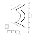
図8A〜8Cは、ポリ-L-リシンの沈積の前および後に行われた差動測定(図8A)、KClの濃度の関数として行われた差動測定(図8B)、および沈積されたポリ-L-リシンの濃度の関数として行われた差動測定を示す。
図8Aにおいて、ドレイン電流IDの変動ΔIDは、X軸上に示されるトランジスタ60〜96のそれぞれについてY軸上に表される(USG = 1 V、USD = 0.9 Vおよび電解質0.1 mMのKCl)。局所沈積の前に行われたが、水でのリンスにより分けられた2つの測定の間の差異ΔIDは、丸形で表される。ポリ-L-リシンの局所沈積の前および後に行われた測定に対応する差異ΔIDは、星形で表される。局所沈積の後、サンプルを、50℃で5分間乾燥させる前に、湿性媒質中で15分間、周囲温度において放置する。ポリ-L-リシンの希釈C0は、pH 7の0.1×PBS緩衝液中に0.01%重量/容積 "W/V"最終濃度(P8920、Sigma)である。
Figures 8A-8C show differential measurements made before and after poly-L-lysine deposition (Figure 8A), differential measurements made as a function of KCl concentration (Figure 8B), and deposited poly It shows a differential measurements made as a function of the concentration of -L- lysine.
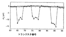
8A, the variations of the drain current I D [Delta] I D is represented on the Y-axis for each of the
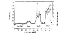
図8Bにおいて、ソース−ゲート電圧USGにおける差異ΔUSGは、USD = 1.2 VおよびID = 50μAの62 FETトランジスタのネットワークのトランジスタのいくつかについて測定される。参照測定(局所沈積の前に、0.01 mMのKClの濃度で行われる)と、2連続の測定(ポリ-L-リシンの局所沈積の後に、種々の濃度のKClで行われる)との間の差異は、丸形および星形で表される。ここで、ポリ-L-リシンの局所沈積は、図8Aの場合と同様に、同じ希釈C0の2つの別個の領域において行われた。2連続の測定のそれぞれにおいて、測定緩衝液中のKClの濃度は、範囲が0.1 mM、1 mMおよび10 mMの値を含む、0.01 mM〜100 mMの間で変動させる。2連続の測定の間に、表面を水でリンスする。ポリ-L-リシンの検出の顕著な感度が、0.01 mMおよび1 mMの間のKCl濃度について観察され、これらの値を超えると、ピークの高さは徐々に減少する。 In Figure 8B, the source - the difference in the gate voltage U SG .DELTA.U SG is measured for several of the transistors of the network 62 FET transistors of U SD = 1.2 V and I D = 50 .mu.A. Between a reference measurement (taken at a concentration of 0.01 mM KCl before local deposition) and two consecutive measurements (taken at various concentrations of KCl after local deposition of poly-L-lysine) Differences are represented by round and star shapes. Here, the local deposition of poly -L- lysine, as in the case of FIG. 8A, was performed in two separate regions of the same dilution C 0. In each of the two consecutive measurements, the concentration of KCl in the measurement buffer is varied between 0.01 mM and 100 mM, including values in the range 0.1 mM, 1 mM and 10 mM. Rinse the surface with water between two consecutive measurements. Significant sensitivity of poly-L-lysine detection is observed for KCl concentrations between 0.01 mM and 1 mM, beyond which the peak height gradually decreases.
図8Cは、沈積されたポリマー(ポリ-L-リシン)の濃度、すなわち0.1×PBS 緩衝液、pH 7中の2C0、C0、C0/2、C0/4、C0/8 (C0は、図8Aの測定で示される値を有する)の関数として、電圧USGにおける変動ΔUSGを示す。測定条件は次のとおりである:USD = 1 V、ID = 100μA、およびKClについて0.01 mMの濃度。これらの測定は、選択された実験的条件下で、C0を超えて濃度を増加させることに利点がないことを示す。
Figure 8C, the concentration of deposited polymer (poly -L- lysine), i.e. 0.1 × PBS buffer, 2C 0 in pH 7, C 0, C 0 /2,
図9A〜9Dは、DNAの電子検出を示す。電圧USGおよび電圧USGにおける変動ΔUSGは、USD = 1 V、ID = 100μA、および0.01 mMのKCl濃度の動作点に対応する。これらは、特性ID(USG、USD)から得られ、そしてX軸上のFETトランジスタ番号(1〜96)とともにカーブに記録される。 Figures 9A-9D show the electronic detection of DNA. Variations in the voltage U SG and the voltage U SG .DELTA.U SG is, U SD = 1 V, corresponding to an operating point of KCl concentration of I D = 100μA, and 0.01 mM. These characteristics I D (U SG, U SD ) obtained from, and recorded to the curve with FET transistors numbers on the X-axis (1-96).
星形は、図6に関して上で示したような、水酸化ナトリウムでの最初の表面処理の前の測定を表す。丸形は、全体のネットワーク上でのポリ-L-リシンのインキュベーションの後の測定を表す。DNAの固定を許容するために、FETトランジスタのネットワークを、ポリ-L-リシン(濃度C0)の希釈中に30分間インキュベーションする。次いで、いずれの予めの乾燥もなしに、水でリンスを行い、その後、空気乾燥する。インキュベーションにより、電圧USGにおいて97±50 mV (準備された67を超える表面の統計的な値)の値のシフトとなり、これが電子シグナルにおけるトランジスタ間の変動を減少させる。このシフトは、同じ濃度で局所沈積について図8Cに関して測定された値で観察されたものと矛盾しない。四角形は、トランジスタ番号30、60および90の周囲でのオリゴヌクレオチド(5' Cy-5修飾された20マーのオリゴヌクレオチド、脱イオン水中に濃度50μM)の局所沈積の後の測定を表す。上記の3つのDNAの点の微蛍光のイメージを、グレー水準で図9Aの上に表す。
The star represents the measurement prior to the first surface treatment with sodium hydroxide, as shown above with respect to FIG. Circles represent measurements after incubation of poly-L-lysine on the entire network. In order to allow DNA fixation, the FET transistor network is incubated for 30 minutes during the dilution of poly-L-lysine (concentration C 0 ). It is then rinsed with water without any prior drying and then air dried. Incubation, in the shift value of 97 ± 50 mV in voltage U SG (statistical value of prepared 67 greater than the surface), which reduces the variation between transistors in the electronic signal. This shift is consistent with that observed with the values measured for FIG. 8C for local deposition at the same concentration. Squares represent measurements after local deposition of oligonucleotides around
図9Bは、Cy5修飾されたオリゴヌクレオチドの電気的検出、および蛍光による検出を示す。星形で表される点は、DNAの異なる濃度(Ref. = 0μM、5μM、10μM、20μM)での4つの局所沈積の前および後に行われた2つの電子測定の間の差異ΔUSGにより得られた。これらは、トランジスタの特性において観察され、かつDNAの局所沈積による電圧USGにおける変動ΔUSGを示す。四角は、電解質を用いて電子測定が一度行われた、乾燥されたFETトランジスタ上で測定された蛍光強度を示す。同じ電子検出が、同じタイプであるが、修飾されていないオリゴヌクレオチドから得られることが記載される。 FIG. 9B shows electrical detection of Cy5 modified oligonucleotides and detection by fluorescence. The point represented by the star shape is obtained by the difference ΔU SG between the two electron measurements made before and after the four local depositions at different concentrations of DNA (Ref. = 0 μM, 5 μM, 10 μM, 20 μM). It was. These are observed in the characteristics of the transistor and show a variation ΔU SG in the voltage U SG due to local deposition of DNA. The squares indicate the fluorescence intensity measured on the dried FET transistor once the electron measurement was made using the electrolyte. It is described that the same electronic detection is obtained from oligonucleotides of the same type but not modified.
図9Cは、FETトランジスタの2つのゾーンAおよびB上への2つの産物の巨視的沈積後の、二本鎖DNAの検出を示す。2つのチューブAおよびBから採取された0.15μlを、マイクロピペットを用いて、FET電界効果形トランジスタのネットワークの2つのそれぞれの領域上に沈積させる。ネットワークは、DNAを固定するためにポリ-L-リシンで予め被覆され、参照となるように測定された。図9CのゾーンA (トランジスタ1〜20)は、チューブAからの溶液で、そしてゾーンB (トランジスタ50〜90)は、チューブBからの溶液で被覆され、それらの間に被覆されていない中央領域(トランジスタ21〜49)が残ることを許容する。インキュベーションは、乾燥せずに15分間行い、その後、水でリンスし、次いでネットワークのトランジスタを測定する。トランジスタ1〜20 (ゾーンA)を、以下に記載される手順に従ってチューブAで得られるポリメラーゼ連鎖反応法(PCR)の産物を含む溶液とインキュベートした。ゾーンB (トランジスタ50〜90)との比較、およびAとBとの間の、上記のインキュベートしていないゾーンとの比較で、このゾーンにおいて下方へのシフトが見られる。実際に、ゾーンBで用いられる参照溶液は、二本鎖DNAを産生しないように選択された(以下に記載の手順によるチューブB)。 FIG. 9C shows the detection of double stranded DNA after macroscopic deposition of the two products on the two zones A and B of the FET transistor. 0.15 μl taken from the two tubes A and B is deposited on the two respective regions of the FET field effect transistor network using a micropipette. The network was pre-coated with poly-L-lysine to immobilize DNA and measured as a reference. Zone A (transistors 1-20) in FIG. 9C is coated with the solution from tube A, and zone B (transistors 50-90) is coated with the solution from tube B, with a central region not covered between them. Allow (transistors 21-49) to remain. Incubation is carried out for 15 minutes without drying, followed by rinsing with water and then measuring the transistors of the network. Transistors 1-20 (zone A) were incubated with a solution containing the product of the polymerase chain reaction (PCR) obtained in tube A according to the procedure described below. In comparison to zone B (transistors 50-90) and in comparison to the above unincubated zone between A and B, a downward shift is seen in this zone. In fact, the reference solution used in Zone B was chosen not to produce double stranded DNA (tube B according to the procedure described below).
図9Dでは、以下に記載の条件下でPCR増幅により得られた溶液がその上に沈積されているMUT領域(トランジスタ1〜35)において、変異を有するDNAから、ΔUSGの下方へのシフトが観察されるのに対して、出発DNAは変異を有さない参照領域WTにおいては、このようなシフトは観察されない。 In FIG. 9D, the MUT region (transistors 1-35) solution obtained by PCR amplification is deposited thereon under the conditions described below, the DNA having a mutation, a shift downward .DELTA.U SG In contrast to this, such a shift is not observed in the reference region WT in which the starting DNA has no mutation.
図9Cの実験について、1009塩基対DNA断片のPCR増幅のための技術は、2つのプライマー:
5'-CCG CGA ACT GAC TCT CCG CC
および
5'-CAG GCG GCA GGG CTG ACG TT
を用いて、BstEII酵素で消化したバクテリオファージλDNAを用いる。
For the experiment in Figure 9C, the technique for PCR amplification of a 1009 base pair DNA fragment has two primers:
5'-CCG CGA ACT GAC TCT CCG CC
and
5'-CAG GCG GCA GGG CTG ACG TT
Using bacteriophage λ DNA digested with BstEII enzyme.
PCRプロトコルは、市販のサーモサイクラーで:
−94℃で3分間の開始、
−94℃で30秒/57℃で30秒/および72℃で2分間の、変性/ハイブリダイズ/伸長の30サイクル
で行われる。
最後のPCR工程は、72℃で3分間行われる。
The PCR protocol is a commercially available thermocycler:
Start at −94 ° C. for 3 minutes,
30 cycles of denaturation / hybridization / extension at −94 ° C. for 30 seconds / 57 ° C. for 30 seconds / and 72 ° C. for 2 minutes.
The final PCR step is performed at 72 ° C for 3 minutes.
50μlの容積について、BstEIIで消化されたλDNA 10 ng、各プライマーについて20ピコモル、およびそれぞれ最終濃度50μMをもつ4つのdNTPを用いる。ロシュディアグノスティクスからのTAQポリメラーゼ(1U/μl) 0.5μlを、標準のPCR反応緩衝液(TAQポリメラーゼとともに供給される)中に入れる。これは、ゾーンAへのチューブAからの調製に対応する。参照チューブB(ゾーンBに対応する)では、4つのdNTPの1つ、すなわちdTTPを、dNTPの全濃度が同じに保持されるような様式でdCTPと置換し、これが二本鎖DNA産物の合成を阻害する。
For a 50 μl volume,
両方の場合において、PCR産物を、キアゲン社からの"QIAQUICK"カラムで2回精製し、濃度10 mMにおいて、Tris-Cl緩衝液、pH 8.5で溶出する。 In both cases, the PCR product is purified twice on a “QIAQUICK” column from Qiagen and eluted with Tris-Cl buffer, pH 8.5, at a concentration of 10 mM.
図9Dに対応する実験の関係において用いられる変異の具体的なPCR増幅は、ヒトCX 26遺伝子(受理コードM 86849、染色体13q11-12)の断片に基づく。この遺伝子は、1以上の患者を起源とするゲノムDNAから増幅される。PCR法は、サイクルプライマー、ならびにHuman Molecular Genetics、1997、第6巻、第12号、第2173〜2177頁に出版されている、最初の"Prelingual Deafness: high prevalence of a 30delG mutation in the connexin 26 gene"、およびTHE LANCET、第353巻、April 17、1999、第1298〜1303頁に出版されている、次の"Clinical features of the prevalent form of childhood deafness, DFNB1, due to a connexin-26 gene defect: implications for genetic counselling"に用いられたF. DENOYELLEらによる論文に記載されている条件を用いる。Pwoポリメラーゼ(ロシュディアグノスティクスより)を、1.5 mMで、MgSO4を用いたPCR緩衝液中で用いる。プライマーは、GAP1FおよびCONNR (上記のF. DENOYELLEによる第二の論文の第1299頁右欄、終わりから2番目のパラグラフを参照)であり、実験条件は、同じ著者による上記の最初の論文(第2177頁)のものである。各プライマーについて0.6μM、各dNTPについて0.2 mMの最終濃度を用いる。 The specific PCR amplification of the mutation used in the experimental context corresponding to FIG. 9D is based on a fragment of the human CX26 gene (acceptance code M86849, chromosome 13q11-12). This gene is amplified from genomic DNA originating from one or more patients. The PCR method is a cycle primer and the first “Prelingual Deafness: high prevalence of a 30delG mutation in the connexin 26 gene, published in Human Molecular Genetics, 1997, Vol. 12, No. 12, pp. 2173-2177. "And published in THE LANCET, Volume 353, April 17, 1999, pages 1298 to 1303," Clinical features of the prevalent form of childhood deafness, DFNB1, due to a connexin-26 gene defect: The conditions described in the paper by F. DENOYELLE et al. used in "implications for genetic counselling" are used. Pwo polymerase (from Roche Diagnostics) is used at 1.5 mM in PCR buffer with MgSO 4 . The primers are GAP1F and CONNR (see the second article from the second article by F. DENOYELLE above, page 1299, right column, second paragraph from the end), and the experimental conditions are the same as the first article (the first article by the same author). 2177). Use a final concentration of 0.6 μM for each primer and 0.2 mM for each dNTP.
PCR産物は、キアゲン社からの"QIAQUICK"カラムで精製し、希釈後(10000倍)に、その後に続いて行う変異に特異的な反応における出発DNAとなる。 The PCR product is purified on a “QIAQUICK” column from Qiagen, and after dilution (10000 fold), becomes the starting DNA in the subsequent reaction specific for the mutation.
PCR増幅は、この変異に特異的なプライマーによる、CX26遺伝子における変異35delG (または30delG)の検出を許容するように選択される。サイクル条件およびプライマーの配列は、"PCR test for diagnosis of the common GJB2 (connexin 26) 35delG mutation on dried blood spots and determination of the carrier frequency in France"の題名で、Molecular and Cellular Probes (2001) 15 第57〜59頁に出版されている、G. LUCOTTEらによる論文に示される。各プライマーオリゴヌクレオチド20ピコモルを、50μlの最終容積に対して用いる。 PCR amplification is selected to allow detection of mutation 35delG (or 30delG) in the CX26 gene with primers specific for this mutation. Cycle conditions and primer sequences are titled “PCR test for diagnosis of the common GJB2 (connexin 26) 35delG mutation on dried blood spots and determination of the carrier frequency in France”, Molecular and Cellular Probes (2001) 15 57 Shown in a paper by G. LUCOTTE et al. 20 pmol of each primer oligonucleotide is used for a final volume of 50 μl.
変異に特異的な2つのプライマー(上記のLUCOTTEによる論文、第58頁右欄、MプライマーおよびNプライマー)、および共通プライマー(Cプライマー)を用いて、197塩基対のPCR産物を合成する。2つの特異的PCR反応を各DNAサンプルについて行い、これらの反応の第一を、第一の特異的プライマーを用いて行い、出発DNAの中に変異が存在すれば産物が得られる。第二の反応は、第二の特異的プライマーを用いて行い、出発DNAの中に変異が存在しなければ産物が得られる。これにより、サンプルが、この変異に関して正常、ヘテロ接合性またはホモ接合性であるかを決定することが可能になる。 A 197 base pair PCR product is synthesized using two primers specific to the mutation (the above-mentioned article by LUCOTTE, page 58, right column, M primer and N primer) and a common primer (C primer). Two specific PCR reactions are performed on each DNA sample, and the first of these reactions is performed using the first specific primer and the product is obtained if the mutation is present in the starting DNA. The second reaction is performed using the second specific primer and the product is obtained if no mutation is present in the starting DNA. This makes it possible to determine whether the sample is normal, heterozygous or homozygous for this mutation.
反応媒質50μlの容積について、標準のPCR緩衝液中に、上記の予めの増幅を起源とするDNA 1μl、各プライマー30ピコモル、100μMの濃度のdNTPおよびロシュディアグノスティクスからのTAQポリメラーゼ(1 U/μl) 1μlを用いる。PCR産物を、キアゲン社からの"QIAQUICK"カラムで2回精製し、10 mMのTris-Cl緩衝液、pH 8.5で溶出する。同じ対のプライマー:C-プライマーおよびM-プライマーを、WTおよびMUTチューブに用いる。出発DNAのみが相違点である。
For a volume of 50 μl of reaction medium, in standard PCR buffer, 1 μl of DNA from the above prior amplification, 30 pmoles of each primer, dNTPs at a concentration of 100 μM and TAQ polymerase from Roche Diagnostics (1 U / μl)
図10Aおよび10Bは、ライン(またはいくつかのライン)に沿って配置されたトランジスタTを有する、組み込まれた回路を示す。基板30の2つのマイクロ流体チャネル(例えば並列のチャネル)C1およびC2は、1以上の電界効果形トランジスタTを、チャネルC1および/またはC2を循環する溶液に接触させることを可能にする。マイクロ流体チャネル(またはキャピラリー)を含む基板30の材料は、PDMS (ポリジメチルシロキサン)またはその他のポリマー、ガラス、シリコンなどであり得る。
FIGS. 10A and 10B show an integrated circuit with a transistor T arranged along a line (or several lines). Two microfluidic channels (eg, parallel channels) C 1 and C 2 on substrate 30 allow one or more field effect transistors T to be in contact with the solution circulating in channels C 1 and / or C 2 To do. The material of the
したがって、2つのチャネルC1および/またはC2を循環する2つの溶液を用いて、差動測定を行うことができる。同じ基板30上に、このようなマイクロ流体チャネルの多数を製造することも可能であり、該基板は、FET電界効果形トランジスタが組み込まれる半導体基板に接触するように配置されている。所定のチャネル内で変動を測定することも可能である。この変動は、時間に関するものであり得る。キャピラリーの所定の位置に種々の溶液を注入することも可能であり、濃度のプロフィールは、注入点からかなりの距離であっても、チャネルに沿って変化しないままである。"Microfabrication inside Capillaries Using Multiphase Laminar Flow Patterning"の題名で、SCIENCE、第285巻、July 2、1999、第83〜85頁で出版されている、Paul J.A. KENISらによる論文(特に図1A)を参照とすることができる。
Thus, differential measurements can be made using two solutions circulating in the two channels C 1 and / or C 2 . Many of such microfluidic channels can be fabricated on the
マイクロ流体工学を用いた分析技術は、Sensors and Actuators B 63 (2000)、第138〜146頁で出版されている、Eric T. LAGALLYらによる論文"Monolithic integrated microfluidic DNA amplification and capillary electrophoresis analysis system"に記載されている。 Analysis techniques using microfluidics are described in the paper "Monolithic integrated microfluidic DNA amplification and capillary electrophoresis analysis system" published by Sensors and Actuators B 63 (2000), pp. 138-146, by Eric T. LAGALLY et al. Are listed.
1 絶縁層
2 絶縁層
3 反応性領域
4 反応性表面
4' 反応性表面
6 電解質
10 ソース
11 テーブル
12 プラットホーム
14 支持体
15 チップ
17 対物レンズ
19 スクリーン
20 プラットホーム
21 テーブル
22 アーム
23 ピペット
DESCRIPTION OF
Claims (17)
a) 分子プローブを固定するために、該ゾーン(3)のいくつかを該プローブと接触させ、
b) 分子プローブと接触された少なくともこれらのゾーンを電解質溶液(6)中に浸し、
c) 分子プローブと接触させた少なくとも1つのゾーン(3)に対応する第一群のトランジスタ中の少なくとも2つに特徴的なドレイン電流/ソース−ゲート電圧/ソース−ドレイン電圧の少なくとも1点を測定し、2つの異なるゾーンについて得られた少なくとも2つの測定の間の比較により、少なくとも1つの固定又は相互作用をそこから導出する
ことを含むことを特徴とする方法。A method for detecting the immobilization or interaction of a molecular probe to a reactive zone of a sensor, the sensor comprising a network of field effect transistors (T 1 , T 2, etc.), each transistor being a source region (S ), The drain region (D), and the gate electrode (E) immersed in the electrolyte solution (6) by fixing the potential of the electrolyte solution (6) covering the reactive zone (3), thereby fixing or Having a gate region (G) forming a reactive zone (3) in which the interaction is to be detected, and the following steps:
a) to immobilize a molecular probe, contact some of the zones (3) with the probe;
b) Immerse at least these zones in contact with the molecular probe in the electrolyte solution (6),
c) Measuring at least one characteristic drain current / source-gate voltage / source-drain voltage in at least two of the first group of transistors corresponding to at least one zone (3) in contact with the molecular probe. And deriving at least one fixation or interaction therefrom by comparison between at least two measurements obtained for two different zones.
a1) リンスを行い、
a2) 分子プローブと特異的に相互作用しうる標的分子を含む溶液を添加する
を、a)の後であってb)の前に含むことを特徴とする請求項1〜3のいずれか1つに記載の方法。Next step:
a1) Rinse and
The method according to any one of claims 1 to 3, wherein a2) a solution containing a target molecule capable of specifically interacting with the molecular probe is added after a) and before b). The method described in 1.
d) 分子プローブと特異的に相互作用し得る標的分子を含む電解質溶液(6)を添加し、
e) 少なくとも1つの固定または相互作用を比較により得るように、分子プローブおよび標的分子と接触させたゾーン(3)に対応する第二群のトランジスタの少なくとも2つに特徴的なドレイン電流/ソース−ゲート電圧/ソース−ドレイン電圧の少なくとも1点を測定する
を、cの後に含むことを特徴とする請求項1〜4のいずれか1つに記載の方法。Next step:
d) Add an electrolyte solution (6) containing a target molecule that can interact specifically with the molecular probe,
e) Drain current / source characteristic of at least two of the second group of transistors corresponding to the zone (3) in contact with the molecular probe and the target molecule so that at least one fixation or interaction is obtained by comparison The method according to claim 1, wherein measuring at least one point of gate voltage / source-drain voltage is included after c.
Applications Claiming Priority (3)
| Application Number | Priority Date | Filing Date | Title |
|---|---|---|---|
| FR0200676A FR2835058B1 (en) | 2002-01-21 | 2002-01-21 | METHOD FOR DETECTING AT LEAST ONE CHARACTERISTIC PARAMETER OF PROBE MOLECULES FIXED ON AT LEAST ONE ACTIVE ZONE OF A SENSOR |
| FR02/00676 | 2002-01-21 | ||
| PCT/FR2002/004283 WO2003062811A1 (en) | 2002-01-21 | 2002-12-11 | Detection of molecular probes fixed to an active zone of a sensor |
Publications (4)
| Publication Number | Publication Date |
|---|---|
| JP2005515475A JP2005515475A (en) | 2005-05-26 |
| JP2005515475A6 JP2005515475A6 (en) | 2005-08-04 |
| JP2005515475A5 JP2005515475A5 (en) | 2006-01-19 |
| JP4500547B2 true JP4500547B2 (en) | 2010-07-14 |
Family
ID=27589525
Family Applications (1)
| Application Number | Title | Priority Date | Filing Date |
|---|---|---|---|
| JP2003562625A Expired - Lifetime JP4500547B2 (en) | 2002-01-21 | 2002-12-11 | Detection of molecular probes immobilized in the reactive zone of the sensor |
Country Status (8)
| Country | Link |
|---|---|
| US (1) | US7993825B2 (en) |
| EP (1) | EP1468277B1 (en) |
| JP (1) | JP4500547B2 (en) |
| AT (1) | ATE366321T1 (en) |
| DE (1) | DE60221046T2 (en) |
| ES (1) | ES2289176T3 (en) |
| FR (1) | FR2835058B1 (en) |
| WO (1) | WO2003062811A1 (en) |
Families Citing this family (36)
| Publication number | Priority date | Publication date | Assignee | Title |
|---|---|---|---|---|
| US7317216B2 (en) * | 2003-10-31 | 2008-01-08 | University Of Hawaii | Ultrasensitive biochemical sensing platform |
| US20080009002A1 (en) * | 2004-11-09 | 2008-01-10 | The Regents Of The University Of California | Analyte Identification Using Electronic Devices |
| KR100773549B1 (en) | 2006-04-03 | 2007-11-07 | 삼성전자주식회사 | Method of detecting bio-molecules using the same field effect transistor |
| KR100773550B1 (en) * | 2006-04-03 | 2007-11-07 | 삼성전자주식회사 | Method of detecting bio-molecules using field effect transistor without fixing bio-molecules |
| KR101195612B1 (en) * | 2006-04-10 | 2012-10-29 | 삼성전자주식회사 | A field effect transistor comprising a gold layer, a microfluidic device comprising the field effect transistor and a method of detecting an analyte having a thiol group using the field effect transistor and microfluidic device |
| US8349167B2 (en) | 2006-12-14 | 2013-01-08 | Life Technologies Corporation | Methods and apparatus for detecting molecular interactions using FET arrays |
| CN101669026B (en) | 2006-12-14 | 2014-05-07 | 生命技术公司 | Methods and apparatus for measuring analytes using large scale FET arrays |
| US11339430B2 (en) | 2007-07-10 | 2022-05-24 | Life Technologies Corporation | Methods and apparatus for measuring analytes using large scale FET arrays |
| US8262900B2 (en) | 2006-12-14 | 2012-09-11 | Life Technologies Corporation | Methods and apparatus for measuring analytes using large scale FET arrays |
| US8198658B2 (en) * | 2007-06-13 | 2012-06-12 | Samsung Electronics Co., Ltd. | Device and method for detecting biomolecules using adsorptive medium and field effect transistor |
| KR101375547B1 (en) * | 2007-06-19 | 2014-03-25 | 삼성전자주식회사 | Biomolecule detector based on field effect transistor arrays containing reference electrodes and detection method for biomolecules using the same |
| US20100301398A1 (en) | 2009-05-29 | 2010-12-02 | Ion Torrent Systems Incorporated | Methods and apparatus for measuring analytes |
| US20100137143A1 (en) | 2008-10-22 | 2010-06-03 | Ion Torrent Systems Incorporated | Methods and apparatus for measuring analytes |
| US20120261274A1 (en) | 2009-05-29 | 2012-10-18 | Life Technologies Corporation | Methods and apparatus for measuring analytes |
| US8776573B2 (en) | 2009-05-29 | 2014-07-15 | Life Technologies Corporation | Methods and apparatus for measuring analytes |
| JP5952813B2 (en) * | 2010-06-30 | 2016-07-13 | ライフ テクノロジーズ コーポレーション | Method and apparatus for testing ISFET arrays |
| US8858782B2 (en) | 2010-06-30 | 2014-10-14 | Life Technologies Corporation | Ion-sensing charge-accumulation circuits and methods |
| CN109449171A (en) | 2010-06-30 | 2019-03-08 | 生命科技公司 | For detecting and measuring the transistor circuit of chemical reaction and compound |
| US11307166B2 (en) | 2010-07-01 | 2022-04-19 | Life Technologies Corporation | Column ADC |
| WO2012006222A1 (en) | 2010-07-03 | 2012-01-12 | Life Technologies Corporation | Chemically sensitive sensor with lightly doped drains |
| WO2012036679A1 (en) | 2010-09-15 | 2012-03-22 | Life Technologies Corporation | Methods and apparatus for measuring analytes |
| US9970984B2 (en) | 2011-12-01 | 2018-05-15 | Life Technologies Corporation | Method and apparatus for identifying defects in a chemical sensor array |
| US8786331B2 (en) | 2012-05-29 | 2014-07-22 | Life Technologies Corporation | System for reducing noise in a chemical sensor array |
| US9080968B2 (en) | 2013-01-04 | 2015-07-14 | Life Technologies Corporation | Methods and systems for point of use removal of sacrificial material |
| US9841398B2 (en) | 2013-01-08 | 2017-12-12 | Life Technologies Corporation | Methods for manufacturing well structures for low-noise chemical sensors |
| US8963216B2 (en) | 2013-03-13 | 2015-02-24 | Life Technologies Corporation | Chemical sensor with sidewall spacer sensor surface |
| US9835585B2 (en) | 2013-03-15 | 2017-12-05 | Life Technologies Corporation | Chemical sensor with protruded sensor surface |
| WO2014149779A1 (en) | 2013-03-15 | 2014-09-25 | Life Technologies Corporation | Chemical device with thin conductive element |
| US20140264472A1 (en) | 2013-03-15 | 2014-09-18 | Life Technologies Corporation | Chemical sensor with consistent sensor surface areas |
| US20140336063A1 (en) | 2013-05-09 | 2014-11-13 | Life Technologies Corporation | Windowed Sequencing |
| US10458942B2 (en) | 2013-06-10 | 2019-10-29 | Life Technologies Corporation | Chemical sensor array having multiple sensors per well |
| WO2016100486A1 (en) | 2014-12-18 | 2016-06-23 | Life Technologies Corporation | High data rate integrated circuit with transmitter configuration |
| US10077472B2 (en) | 2014-12-18 | 2018-09-18 | Life Technologies Corporation | High data rate integrated circuit with power management |
| CN111505087A (en) | 2014-12-18 | 2020-08-07 | 生命科技公司 | Method and apparatus for measuring analytes using large scale FET arrays |
| US11293897B2 (en) * | 2018-11-30 | 2022-04-05 | Taiwan Semiconductor Manufacturing Company, Ltd. | High sensitivity ISFET sensor |
| GB202017861D0 (en) | 2020-11-12 | 2020-12-30 | Ulifetec Sas | Method |
Family Cites Families (21)
| Publication number | Priority date | Publication date | Assignee | Title |
|---|---|---|---|---|
| US4238757A (en) * | 1976-03-19 | 1980-12-09 | General Electric Company | Field effect transistor for detection of biological reactions |
| EP0213825A3 (en) * | 1985-08-22 | 1989-04-26 | Molecular Devices Corporation | Multiple chemically modulated capacitance |
| US5200051A (en) * | 1988-11-14 | 1993-04-06 | I-Stat Corporation | Wholly microfabricated biosensors and process for the manufacture and use thereof |
| US5242793A (en) * | 1989-03-08 | 1993-09-07 | Kanzaki Paper Manufacturing Co., Ltd. | Selective permeable membrane and electrode using the same |
| US5498521A (en) * | 1990-01-24 | 1996-03-12 | President And Fellows Of Harvard College | Diagnosis of hereditary retinal degenerative diseases |
| AU2907092A (en) * | 1991-10-21 | 1993-05-21 | James W. Holm-Kennedy | Method and device for biochemical sensing |
| US5846708A (en) * | 1991-11-19 | 1998-12-08 | Massachusetts Institiute Of Technology | Optical and electrical methods and apparatus for molecule detection |
| CA2134552A1 (en) * | 1992-04-27 | 1993-11-11 | George D. Sorenson | Detection of gene sequences in biological fluids |
| US6331274B1 (en) * | 1993-11-01 | 2001-12-18 | Nanogen, Inc. | Advanced active circuits and devices for molecular biological analysis and diagnostics |
| US5856174A (en) * | 1995-06-29 | 1999-01-05 | Affymetrix, Inc. | Integrated nucleic acid diagnostic device |
| US5805014A (en) * | 1996-03-01 | 1998-09-08 | Compaq Computer Corporation | System having active pull-down circuit and method |
| EP0894148A4 (en) * | 1996-04-17 | 1999-06-16 | Motorola Inc | Transistor-based molecular detection apparatus and method |
| US5827482A (en) * | 1996-08-20 | 1998-10-27 | Motorola Corporation | Transistor-based apparatus and method for molecular detection and field enhancement |
| US6322963B1 (en) * | 1998-06-15 | 2001-11-27 | Biosensor Systems Design., Inc. | Sensor for analyte detection |
| US6281006B1 (en) * | 1998-08-24 | 2001-08-28 | Therasense, Inc. | Electrochemical affinity assay |
| US6875619B2 (en) * | 1999-11-12 | 2005-04-05 | Motorola, Inc. | Microfluidic devices comprising biochannels |
| FR2805826B1 (en) * | 2000-03-01 | 2002-09-20 | Nucleica | NEW DNA CHIPS |
| EP1134294A3 (en) * | 2000-03-16 | 2004-06-30 | Kabushiki Kaisha Toshiba | Method for producing immobilized nucleic acid strand |
| EP1423687A1 (en) * | 2001-08-08 | 2004-06-02 | The Arizona Board of Regents | Nucleic acid field effect transistor |
| US20050170347A1 (en) * | 2001-12-19 | 2005-08-04 | Yuji Miyahara | Potentiometric dna microarray, process for producing the same and method of analyzing nucleic acid |
| AU2003260662A1 (en) * | 2002-12-11 | 2004-07-14 | Centre National De La Recherche Scientifique | Method for electronically detecting at least one specific interaction between probe molecules and target biomolecules |
-
2002
- 2002-01-21 FR FR0200676A patent/FR2835058B1/en not_active Expired - Fee Related
- 2002-12-11 AT AT02799807T patent/ATE366321T1/en not_active IP Right Cessation
- 2002-12-11 US US10/501,772 patent/US7993825B2/en active Active
- 2002-12-11 DE DE60221046T patent/DE60221046T2/en not_active Expired - Lifetime
- 2002-12-11 ES ES02799807T patent/ES2289176T3/en not_active Expired - Lifetime
- 2002-12-11 EP EP02799807A patent/EP1468277B1/en not_active Expired - Lifetime
- 2002-12-11 WO PCT/FR2002/004283 patent/WO2003062811A1/en active IP Right Grant
- 2002-12-11 JP JP2003562625A patent/JP4500547B2/en not_active Expired - Lifetime
Also Published As
| Publication number | Publication date |
|---|---|
| US7993825B2 (en) | 2011-08-09 |
| ES2289176T3 (en) | 2008-02-01 |
| DE60221046D1 (en) | 2007-08-16 |
| ATE366321T1 (en) | 2007-07-15 |
| JP2005515475A (en) | 2005-05-26 |
| DE60221046T2 (en) | 2008-03-06 |
| FR2835058A1 (en) | 2003-07-25 |
| US20060011911A1 (en) | 2006-01-19 |
| EP1468277A1 (en) | 2004-10-20 |
| FR2835058B1 (en) | 2004-03-12 |
| WO2003062811A1 (en) | 2003-07-31 |
| EP1468277B1 (en) | 2007-07-04 |
Similar Documents
| Publication | Publication Date | Title |
|---|---|---|
| JP4500547B2 (en) | Detection of molecular probes immobilized in the reactive zone of the sensor | |
| JP2005515475A6 (en) | Detection of molecular probes immobilized in the reactive zone of the sensor | |
| US20230333039A1 (en) | An active-electrode integrated biosensor array and methods for use thereof | |
| JP3874772B2 (en) | Biologically related substance measuring apparatus and measuring method | |
| JP4857820B2 (en) | DNA sensing method | |
| US7908088B2 (en) | Method for electronically detecting at least one specific interaction between probe molecules and target biomolecules | |
| US20090153130A1 (en) | Field effect transistor-based biosensor with inorganic film, method of manufacturing the biosensor, and method of detecting biomolecule using the biosensor | |
| US9804120B2 (en) | Systems and methods for multiplexed electrochemical detection | |
| US20050106587A1 (en) | Method for determining of nucleic acid analytes | |
| EP1664755A1 (en) | Detection of molecular interactions using a field effect transistor | |
| US20120058547A1 (en) | Method and system for nucleic acid detection using electroconductive or electrochemically active labels | |
| Berdat et al. | DNA biosensor using fluorescence microscopy and impedance spectroscopy | |
| Bronder et al. | Detection of PCR-amplified tuberculosis DNA fragments with polyelectrolyte-modified field-effect sensors | |
| TW200301307A (en) | Method for determining nucleic acid analytes | |
| US8975025B2 (en) | Method and system for nucleic acid detection using electroconductive or electrochemically active labels | |
| JP3934609B2 (en) | Method and biosensor for detecting high molecular weight biopolymers | |
| US20210140917A1 (en) | Devices and methods for detecting/discriminating complementary and mismatched nucleic acids using ultrathin film field-effect transistors |
Legal Events
| Date | Code | Title | Description |
|---|---|---|---|
| A521 | Request for written amendment filed |
Free format text: JAPANESE INTERMEDIATE CODE: A523 Effective date: 20051121 |
|
| A621 | Written request for application examination |
Free format text: JAPANESE INTERMEDIATE CODE: A621 Effective date: 20051121 |
|
| A977 | Report on retrieval |
Free format text: JAPANESE INTERMEDIATE CODE: A971007 Effective date: 20081106 |
|
| A131 | Notification of reasons for refusal |
Free format text: JAPANESE INTERMEDIATE CODE: A131 Effective date: 20081202 |
|
| A521 | Request for written amendment filed |
Free format text: JAPANESE INTERMEDIATE CODE: A523 Effective date: 20090226 |
|
| A131 | Notification of reasons for refusal |
Free format text: JAPANESE INTERMEDIATE CODE: A131 Effective date: 20090929 |
|
| A521 | Request for written amendment filed |
Free format text: JAPANESE INTERMEDIATE CODE: A523 Effective date: 20091208 |
|
| TRDD | Decision of grant or rejection written | ||
| A01 | Written decision to grant a patent or to grant a registration (utility model) |
Free format text: JAPANESE INTERMEDIATE CODE: A01 Effective date: 20100323 |
|
| A01 | Written decision to grant a patent or to grant a registration (utility model) |
Free format text: JAPANESE INTERMEDIATE CODE: A01 |
|
| A61 | First payment of annual fees (during grant procedure) |
Free format text: JAPANESE INTERMEDIATE CODE: A61 Effective date: 20100419 |
|
| FPAY | Renewal fee payment (event date is renewal date of database) |
Free format text: PAYMENT UNTIL: 20130423 Year of fee payment: 3 |
|
| R150 | Certificate of patent or registration of utility model |
Ref document number: 4500547 Country of ref document: JP Free format text: JAPANESE INTERMEDIATE CODE: R150 Free format text: JAPANESE INTERMEDIATE CODE: R150 |
|
| FPAY | Renewal fee payment (event date is renewal date of database) |
Free format text: PAYMENT UNTIL: 20140423 Year of fee payment: 4 |
|
| R250 | Receipt of annual fees |
Free format text: JAPANESE INTERMEDIATE CODE: R250 |
|
| S111 | Request for change of ownership or part of ownership |
Free format text: JAPANESE INTERMEDIATE CODE: R313113 |
|
| R360 | Written notification for declining of transfer of rights |
Free format text: JAPANESE INTERMEDIATE CODE: R360 |
|
| R250 | Receipt of annual fees |
Free format text: JAPANESE INTERMEDIATE CODE: R250 |
|
| R360 | Written notification for declining of transfer of rights |
Free format text: JAPANESE INTERMEDIATE CODE: R360 |
|
| R371 | Transfer withdrawn |
Free format text: JAPANESE INTERMEDIATE CODE: R371 |
|
| S111 | Request for change of ownership or part of ownership |
Free format text: JAPANESE INTERMEDIATE CODE: R313117 Free format text: JAPANESE INTERMEDIATE CODE: R313113 |
|
| R350 | Written notification of registration of transfer |
Free format text: JAPANESE INTERMEDIATE CODE: R350 |
|
| R250 | Receipt of annual fees |
Free format text: JAPANESE INTERMEDIATE CODE: R250 |
|
| R250 | Receipt of annual fees |
Free format text: JAPANESE INTERMEDIATE CODE: R250 |
|
| R250 | Receipt of annual fees |
Free format text: JAPANESE INTERMEDIATE CODE: R250 |
|
| R250 | Receipt of annual fees |
Free format text: JAPANESE INTERMEDIATE CODE: R250 |
|
| R250 | Receipt of annual fees |
Free format text: JAPANESE INTERMEDIATE CODE: R250 |
|
| R250 | Receipt of annual fees |
Free format text: JAPANESE INTERMEDIATE CODE: R250 |
|
| R250 | Receipt of annual fees |
Free format text: JAPANESE INTERMEDIATE CODE: R250 |
|
| R250 | Receipt of annual fees |
Free format text: JAPANESE INTERMEDIATE CODE: R250 |
|
| EXPY | Cancellation because of completion of term |