JP4497650B2 - Laser oscillation apparatus, exposure apparatus, and semiconductor device manufacturing method - Google Patents
Laser oscillation apparatus, exposure apparatus, and semiconductor device manufacturing method Download PDFInfo
- Publication number
- JP4497650B2 JP4497650B2 JP2000126502A JP2000126502A JP4497650B2 JP 4497650 B2 JP4497650 B2 JP 4497650B2 JP 2000126502 A JP2000126502 A JP 2000126502A JP 2000126502 A JP2000126502 A JP 2000126502A JP 4497650 B2 JP4497650 B2 JP 4497650B2
- Authority
- JP
- Japan
- Prior art keywords
- oscillation
- wavelength
- laser
- exposure
- oscillation wavelength
- Prior art date
- Legal status (The legal status is an assumption and is not a legal conclusion. Google has not performed a legal analysis and makes no representation as to the accuracy of the status listed.)
- Expired - Fee Related
Links
Images


Classifications
-
- H—ELECTRICITY
- H01—ELECTRIC ELEMENTS
- H01S—DEVICES USING THE PROCESS OF LIGHT AMPLIFICATION BY STIMULATED EMISSION OF RADIATION [LASER] TO AMPLIFY OR GENERATE LIGHT; DEVICES USING STIMULATED EMISSION OF ELECTROMAGNETIC RADIATION IN WAVE RANGES OTHER THAN OPTICAL
- H01S3/00—Lasers, i.e. devices using stimulated emission of electromagnetic radiation in the infrared, visible or ultraviolet wave range
- H01S3/14—Lasers, i.e. devices using stimulated emission of electromagnetic radiation in the infrared, visible or ultraviolet wave range characterised by the material used as the active medium
- H01S3/22—Gases
- H01S3/223—Gases the active gas being polyatomic, i.e. containing two or more atoms
- H01S3/225—Gases the active gas being polyatomic, i.e. containing two or more atoms comprising an excimer or exciplex
-
- H—ELECTRICITY
- H01—ELECTRIC ELEMENTS
- H01S—DEVICES USING THE PROCESS OF LIGHT AMPLIFICATION BY STIMULATED EMISSION OF RADIATION [LASER] TO AMPLIFY OR GENERATE LIGHT; DEVICES USING STIMULATED EMISSION OF ELECTROMAGNETIC RADIATION IN WAVE RANGES OTHER THAN OPTICAL
- H01S3/00—Lasers, i.e. devices using stimulated emission of electromagnetic radiation in the infrared, visible or ultraviolet wave range
- H01S3/10—Controlling the intensity, frequency, phase, polarisation or direction of the emitted radiation, e.g. switching, gating, modulating or demodulating
- H01S3/102—Controlling the intensity, frequency, phase, polarisation or direction of the emitted radiation, e.g. switching, gating, modulating or demodulating by controlling the active medium, e.g. by controlling the processes or apparatus for excitation
- H01S3/104—Controlling the intensity, frequency, phase, polarisation or direction of the emitted radiation, e.g. switching, gating, modulating or demodulating by controlling the active medium, e.g. by controlling the processes or apparatus for excitation in gas lasers
-
- H—ELECTRICITY
- H01—ELECTRIC ELEMENTS
- H01S—DEVICES USING THE PROCESS OF LIGHT AMPLIFICATION BY STIMULATED EMISSION OF RADIATION [LASER] TO AMPLIFY OR GENERATE LIGHT; DEVICES USING STIMULATED EMISSION OF ELECTROMAGNETIC RADIATION IN WAVE RANGES OTHER THAN OPTICAL
- H01S3/00—Lasers, i.e. devices using stimulated emission of electromagnetic radiation in the infrared, visible or ultraviolet wave range
- H01S3/10—Controlling the intensity, frequency, phase, polarisation or direction of the emitted radiation, e.g. switching, gating, modulating or demodulating
- H01S3/105—Controlling the intensity, frequency, phase, polarisation or direction of the emitted radiation, e.g. switching, gating, modulating or demodulating by controlling the mutual position or the reflecting properties of the reflectors of the cavity, e.g. by controlling the cavity length
- H01S3/1055—Controlling the intensity, frequency, phase, polarisation or direction of the emitted radiation, e.g. switching, gating, modulating or demodulating by controlling the mutual position or the reflecting properties of the reflectors of the cavity, e.g. by controlling the cavity length one of the reflectors being constituted by a diffraction grating
-
- H—ELECTRICITY
- H01—ELECTRIC ELEMENTS
- H01S—DEVICES USING THE PROCESS OF LIGHT AMPLIFICATION BY STIMULATED EMISSION OF RADIATION [LASER] TO AMPLIFY OR GENERATE LIGHT; DEVICES USING STIMULATED EMISSION OF ELECTROMAGNETIC RADIATION IN WAVE RANGES OTHER THAN OPTICAL
- H01S3/00—Lasers, i.e. devices using stimulated emission of electromagnetic radiation in the infrared, visible or ultraviolet wave range
- H01S3/10—Controlling the intensity, frequency, phase, polarisation or direction of the emitted radiation, e.g. switching, gating, modulating or demodulating
- H01S3/106—Controlling the intensity, frequency, phase, polarisation or direction of the emitted radiation, e.g. switching, gating, modulating or demodulating by controlling devices placed within the cavity
Description
【0001】
【発明の属する技術分野】
本発明は、例えばレーザ光の発振波長の変更が可能なレーザ発振装置、それを用いた露光装置、およびその露光装置を用いる半導体デバイス製造方法に関するものである。
【0002】
【従来の技術】
ステップ・アンド・リピート方式或いはステップ・アンド・スキャン方式の露光装置は半導体集積回路の製造工程において中心的役割を担っている。この露光装置はマスク或いはレチクル(以下、レチクルと呼ぶ)の回路パターンを投影レンズを介し、レジストが塗布された被露光基板(以下、ウエハと呼ぶ)面上に露光する。近年、半導体集積回路の集積度はますます高くなる傾向にあり、それに伴い、より短い波長の露光光を発する光源が必要になってきている。特に、レーザ発振装置の一種である希ガスハライドエキシマレーザ(以下、エキシマレーザと呼ぶ)が、紫外域高出力レーザとして注目を集めている。
【0003】
露光装置は通常クリーンルーム内で使用されており、天候の変化などによりクリーンルーム内の気圧が変化するのに伴い、露光光の屈折率が変化し、回路パターンの結像位置が変動してしまう。通常、露光装置用エキシマレーザは発振波長を変更することが可能であり、その可変範囲は300〜400pm程度である。露光光の屈折率は波長によって異なるため、例えばジョブ開始やウエハ交換などの適当なタイミングで、露光装置の使用環境における気圧を計測し、気圧の変化による結像位置の変動を相殺するように発振させるべき最適な発振波長を算出し、エキシマレーザの発振波長を所望の量だけ変更することで、露光装置の使用環境における気圧の変化に対応させている。
【0004】
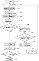
このような露光装置では、図12に示すようなフローで露光が行なわれる。ジョブ開始(ステップ901)後、例えばウエハロード時などのタイミングで投影レンズ近傍の気圧を計測し(ステップ902)、露光装置の主制御部はステップ903でその気圧を基に露光に最適な発振波長(発振波長目標値)を算出し、ステップ904でその発振波長目標値がエキシマレーザの制御部に送信され、ステップ905でエキシマレーザはエキシマレーザ出射口部に設けられたシャッタを閉じ、ステップ906でパルス光を発振させた状態で空打ちを行ない、発振波長をエキシマレーザ内部の光計測部で監視しながら波長変更手段を用いて発振波長を変更し、ステップ907で発振波長が発振波長目標値から所定の許容範囲内に入ったか否かを判断する。発振波長が所定の許容範囲に入らなかった場合、エキシマレーザはエラー状態となり、発振を停止する(ステップ908)。発振波長が所定の許容範囲内に入った場合、ステップ909でそれを知らせる波長ロック信号ONを露光装置側に送信し、シャッタを開け、ステップ910で露光装置側からの発光信号に応じて露光を開始する。露光終了後ウエハアンロードをし(ステップ911)、次のウエハを露光するか判断し(ステップ912)、次のウエハを露光しない場合はジョブ終了とし(ステップ913)、次のウエハを露光する場合はステップ902へ戻る。
【0005】
【発明が解決しようとする課題】
ところが従来例では発振波長を変更する毎に、変更後の発振波長が目標値になったか否かを確認するために、シャッタを閉じて空打ちを行なう必要があり、シャッタの開閉および空打ちに費やす時間だけ露光装置の生産性を低下させてしまっていた。
【0006】
本発明はこのような点を考慮してなされたものであり、このレーザ発振装置を露光装置用光源として使用する際には、露光装置の生産性の低下を招くことなく、常に良好な回路パターンを露光する露光装置、および半導体デバイス製造方法を提供することを目的とする。
【0007】
【課題を解決するための手段】
上述の目的を達成するために、本発明の一側面としてのレーザ発振装置は、波長選択素子を駆動し、レーザ光の発振波長を変更する波長変更手段と、前記レーザ光の発振休止前の発振デューティおよび発振休止時間を記憶する記憶手段と、前記レーザ光を再度発振した際のバースト先頭で発生する発振波長のエラー量を前記記憶手段に記憶された前記発振デューティおよび前記発振休止時間に基づいて算出する算出手段と、を有し、前記波長変更手段は、前記算出手段で算出された前記エラー量に基づいて、前記バースト先頭から前記レーザ光の発振波長が所定の許容範囲内に入ように前記波長選択素子を駆動することを特徴とする。
また、本発明の別の一側面としてのレーザ発振装置は、波長選択素子を駆動し、レーザ光の発振波長を変更する波長変更手段と、前記レーザ光の発振波長が目標値になるように該レーザ光の該発振波長を変更した際のバースト先頭で発生する発振波長のエラー量を前記発振波長の変更量に基づいて算出する算出手段と、を有し、前記波長変更手段は、前記算出手段で算出された前記エラー量に基づいて、前記バースト先頭から前記レーザ光の発振波長が前記目標値になるように前記波長選択素子を駆動することを特徴とする。
【0008】
更にレーザ発振を始めた直後もしくはバースト発振させた場合のバースト先頭から数十・数百パルスのレーザ光の波長は不安定で波長がドリフトしており、そのドリフトの量はレーザの発振履歴やレーザ発振装置内部にある波長計測部内部の環境によって変化することが本発明の発明者らの実験により明らかになった。発振履歴としては、波長の変更幅、発振中止してからの経過時間、発振デューティ(発振時間/休止時間の比率)など、波長計測部内部の環境としては気圧、温度などを挙げることができる。このため本発明のレーザ発振装置では、レーザ発振装置内部にレーザ光の発振履歴を記憶する発振履歴記憶手段および波長計測部内部の環境を計測する波長計測部内環境計測手段のうち一つまたは両方を持ち、発振履歴記憶手段に記録されている発振履歴および前記波長計測部内環境計測手段による計測結果のうち少なくとも一つを用いてレーザ発振装置内部の波長計測部のドリフト量を計算し、その計算結果を考慮して目標波長から所定の許容範囲内の波長で発振させるように波長調整手段を駆動制御することがより好ましい。
【0009】
更に、レーザ発振を休止していた時間が長い場合や波長の変更量が非常に大きい場合には発振開始直後の波長を所望の範囲内に調整することが困難であり、レーザ発振装置が所望の許容範囲の波長で正常に発振しているかの判断も困難となるおそれもあるため、本発明に係るレーザ発振装置の望ましい形態では、発振波長が所定の許容範囲内で発振しているか否かを判断する信号を送信する波長ロック信号送信機能を持ち、発振波長の変更量もしくは発振中止してからの経過時間のうち一つまたは両方にしきい値を設け、上記波長ロック信号の状態はそのしきい値により判断される。
【0010】
また、本発明に係る露光装置では、本発明のレーザ発振装置を光源として用いることにより、波長が所定の許容範囲内に入ったか否かの確認のための空打ちを実行することなく露光を開始する事を特徴とする。もし波長の変更量や発振休止時間が非常に大きい場合や、その他の何らかの理由で波長が所定の許容範囲内に入らない場合は、レーザ発振装置は、波長が所定の範囲内に調整されているか調整されていないかを判断する波長ロック信号を出力として持ち、露光装置はガスレーザ発振装置が波長ロック信号に基づいて空打ちを行うか行わないかの判断をする。本発明の露光装置では、波長変更のタイミングは或る一枚のウエハ交換時以外にも或る露光領域への露光が完了した後、次に露光する領域を露光する前に行っても良い。
【0011】
【発明の実施の形態】
以下、図に示した実施例に基づいて本発明の実施の形態を詳細に説明する。
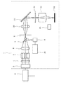
図1は本発明に係る露光装置の一実施例を示す構成図である。この図において、1は一般にステッパ(またはスキャナ)と呼ばれている周知のステップ・アンド・リピート(またはステップ・アンド・スキャン)方式の露光装置本体部、2はエキシマレーザを利用したレーザ光源であり、エキシマレーザとしては例えばKrF(波長248nm)エキシマレーザ、ArF(波長193nm)エキシマレーザ等がある。
【0012】
この露光装置本体部1は、レーザ光源2からレーザ光(ビーム)の光路に沿って、光源2からのレーザ光の断面を所望の形状にするためのビーム整形光学系3、レーザ光の強度を調整するための可変NDフィルタ4、レチクル12面上での照度を均一化させるためにレーザ光を分割して重ねるオプティカルインテグレータ5、オプティカルインテグレータ5を介したレーザ光を集光するコンデンサレンズ6、コンデンサレンズ6からのレーザ光の一部を光検出器8に導くためのビームスプリッタ7、コンデンサレンズ6によってレーザ光が集光される位置の近傍に配置され、レチクル12の面上でレーザ光が照射される範囲を規制するマスキングブレード9、マスキングブレード9の像をレチクル12上に結像する結像レンズ10、およびレーザ光の光路を投影レンズ13の方向に向けるためのミラー11等が設けられて構成されている。
【0013】
かかる光学要素を含む照明光学系を通過してきたレーザ光源2からのレーザ光によってレチクル12は照明され、これによりレチクル12上のパターンは、投影光学系としての投影レンズ13を介して基板としてのウエハ14上の複数のショット領域の一つに、例えば1/2〜1/10に縮小されて投影露光(転写)される。ウエハ14は不図示の移動ステージによって投影レンズ13の光軸に垂直な面に沿って2次元的に移動され、露光ショット領域の露光が終了する毎に次の露光ショット領域が投影レンズ13によってレチクル12のパターンが投影される位置に移動される。
【0014】
15は気圧計であり、これは所定の時間間隔で露光装置内部の気圧を計測するものである。その計測値は露光装置本体部1の主制御部16に送信され、主制御部16はそのときに最適なレーザ光の発振波長(発振波長目標値)を算出し、例えば所定の露光領域における露光が終了してから次の露光領域における露光が開始されるまでの間などのタイミングでレーザ光源2に発振波長目標値信号を送信する。また主制御部16では、レーザ光源2に発光させるためのトリガ信号を送信するとともに、光検出器8で検出されたレーザ光の強度に応じて光電変換処理を行い、それを積算し、露光量制御信号を求め、これをレーザ光源2に送信する。レーザ光源2はこれらの発振波長目標値信号、トリガ信号、露光量制御信号に基づいてレーザ光源2内のユニットを制御する。
【0015】
またレーザ光源2からは、主制御部16に波長ロック信号を送信する。この信号は、実際に発振している波長が発振波長目標値から所定の許容範囲内に入っている場合には波長ロック信号ONとし、そうでない場合は波長ロック信号OFFとなる。波長ロック信号ONの場合、発振波長は目標値に対して所定の許容範囲内であるため、レーザ光源2内のシャッタの開閉動作や空打ちを 行わず直ちにウエハへの露光を開始できる。波長ロック信号OFFの場合は、主制御部16はウエハ14への露光を実施せず、レーザ光源2の出射口部にあるシャッタを閉じて、発振波長を所定の許容範囲内に入れるために空打ちを行い、所定の許容範囲内に入った後にシャッタを開け、再度露光を開始することができる。
【0016】
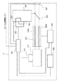
図2は図1に示すレーザ光源2の一例であるエキシマレーザ内部の概略を示す図である。露光装置本体の主制御部16から送信された発振波長目標値信号、トリガ信号、露光量制御信号はレーザ制御部201で受信される。レーザ制御部201は高電圧信号を高圧電源202に送信するとともにレーザを発光させるタイミングでトリガ信号を圧縮回路203に送信する。またレーザ制御部201は発振波長目標値信号を波長制御部204に送信する。レーザチャンバ205内には放電電極205A、205Bが設けられており、圧縮回路203により10〜30kV程度の高電圧が印可されると放電電極205A、205B間で放電が発生し、レーザチャンバ205内に封入されているレーザガスを励起することでレーザ光を発振する。レーザチャンバ205の光射出部には不図示の出力ミラーが取り付けられている。レーザチャンバ205から発振されたレーザ光はビームスプリッタ206を透過してシャッタ207を通って図1で示されているビーム整形光学系3へ出射されるとともに、一部のレーザ光はビームスプリッタ206で反射して光モニタ部208へ導入される。レーザ制御部201は図1中の主制御部16からの命令に従ってシャッタ207の開閉を行う。
【0017】
光モニタ部208ではレーザ光のパルスエネルギ、発振波長を常時モニタしており、計測されたパルスエネルギが露光量目標値に対して所望の値であるか否かを判断して、パルスエネルギが所望の値よりも低い場合は放電電極205A、205Bへの印可電圧を上昇させる信号を、高い場合は印可電圧を降下させる信号をレーザ制御部201から高圧電源回路203に送信する。また波長制御部204はレーザ制御部201から送信された発振波長目標値と光モニタ部208にて計測された発振波長とを比較し、計測された発振波長が発振波長目標値に対して所定の許容範囲内にあるか否かを判断する。発振波長が所定の許容範囲内にある場合は、シャッタ207の開閉動作や空打ちを行わず直ちにウエハへの露光を開始できる。発振波長が所定の許容範囲内に入らない場合は、波長制御部204はレーザ制御部201を介して図1の主制御部16に波長ロック信号OFFを送信する。その後、目標値から外れている場合にはシャッタ207が閉じられ、波長制御部204は波長を所定の範囲に入るように調整する信号をステッピングモータ212に送信する。発振波長が発振波長目標値から所定の許容範囲内に入った時点で波長制御部204は波長ロック信号ONをレーザ制御部201を介して図1に示す主制御部16に送信し、シャッタ207は開かれる。
【0018】
また、光モニタ部208内部には気圧計や温度計といった光モニタ部208の内部環境を計測する光モニタ部内部環境計測手段210が載置してあり、この計測結果を基に光モニタ部208内部環境におけるレーザ光の屈折率などを算出することが可能である。この結果に基づいて光モニタ部208のドリフト量を算出し、光モニタ部208のドリフト量を補正することで、常時安定した発振波長のレーザ光を出力することができる。
【0019】
狭帯域化モジュール211はレーザチャンバ205の光射出部にある不図示の出力ミラーと対になってレーザ共振器を構成しており、レーザ光のスペクトル線幅を半値全幅で約1pm程度に狭帯域化するとともに、付随するステッピングモータ212を駆動させることによって狭帯域化モジュール211内部に内蔵されているグレーティングもしくはエタロンなどの波長選択素子を駆動し、発振波長を変更させることが可能である。このとき、この波長選択素子の駆動量は発振波長目標値に基づいて算出される。波長制御部204はレーザ制御部201から送信された発振波長目標値と光モニタ部208で計測された発振波長とを比較して、レーザ光の発振波長が所定の許容範囲内になるようステッピングモータ212に信号を送信しながら常時発振波長を制御している。また発振波長の発振波長目標値が再度変更された場合には、波長制御部204は、発振波長が変更された発振波長目標値と一致するようにステッピングモータ212を再度駆動させる。再度発振波長を変更する時には、波長制御部204は発振履歴記憶部209に記憶された発振履歴に基づいて、次に発振させるレーザ光の発振波長のドリフト量を予測算出し、その算出結果に基づいてステッピングモータ212を駆動させるようにする事がより好ましい。
【0020】
以下に、本発明の発明者らが行った、エキシマレーザ発振装置の発振波長安定性の実験結果を示す。図3(a)は発振を終了してから再度発振させるまでの発振休止時間a、b(a<b)における発振波長安定性を示すデータである。発振休止時間が大きいbの方が、休止後再度発振させてから数十パルス発振するまでの間で、発振目標値に対してエラー量が大きいことを示している。図3(b)は発振を終了してから再度発振させた場合において、発振休止時間を一定とした場合の、休止前の発振デューティ(Duty)c、d(c<d)における発振波長安定性を示すデータである。休止前の発振デューティが高いdの方が、休止後再度発振させてから数十パルス発振するまでの間で、発振目標値に対してエラー量が大きいことを示している。図3(c)は発振を終了してから、再度発振させる時の発振波長の変更量e、f(e<f)における発振波長安定性を示すデータである。発振波長の変更量が大きいfの方が、休止後再度発振させた直後で、発振目標値に対してエラー量が大きいことを示している。このように、レーザ光の発振開始直後の発振波長安定性は不安定であり、発振休止時間、発振デューティや発振波長の変更量に応じて、バースト先頭の数十〜数百パルスにおいて、チャーピング(Chirping)と呼ばれる波長エラーのうねりが発生することが分かる。
【0021】
本発明では、レーザ制御部201もしくは波長制御部204において、これら図3(a)、(b)および(c)で見られるようなバースト先頭で発生する発振波長のエラー量(ドリフト量)を予測算出し、このドリフト量を打ち消して常時レーザ光が所望の発振波長で発振するようにステッピングモータ212を補正制御する。
【0022】
発振波長のドリフト量を予測算出する一例としては以下の式で近似的に表すことが可能である。
【0023】
【数1】

(1)式で一般にF(λexc.)は発振波長の変更量λexc.が大きいほど大きい値となり、一例として図4に示すようになっている。チャーピングはレーザチャンバ205内部の設計に依存するものである。レーザ発振装置の製造過程において、発振波長のドリフト量を実験的に求めて(1)式のF(λexc.)、A、BおよびCを決定し、これをパラメータとして発振履歴記憶部209内部に記憶しておく。また、気圧計や温度計といった光モニタ部内部環境計測手段210による計測結果を基に光モニタ部208内の内部環境におけるレーザ光の屈折率を算出し、その算出結果を用いて光モニタ部208のドリフト量Dを求める。これらのパラメータを用いて(1)式から発振波長のドリフト量Δλを算出し、バースト先頭から発振波長が所定の許容範囲内に入るように、波長制御部204はステッピングモータ212を駆動させ、発振波長を発振波長目標値に変更する。ここで、ステッピングモータ212に1パルス送信した場合の発振波長の変更量をa(pm/ パルス)とすると、発振波長を常時所望の許容範囲内にするために、波長制御部204はステッピングモータ212にΔλ/ a(パルス)だけ送信すれば、常時所望の許容範囲内の波長で発振することが可能である。発振波長のドリフト量Δλを求める工程は露光装置稼働中の非露光時に定期的に行っても良い。
【0025】
また、発振終了後からの休止時間が大きいほど波長のドリフト量Δλも大きい値となることが本発明の発明者らの実験により明らかになった。発振休止時間が或る量より大きいと発振開始直後のレーザ光の発振波長を所定の許容範囲内に制御することが困難となり、所望の露光性能が達成できない可能性がある。このため、レーザ制御部201もしくは波長制御部204内部に(1)式のF(λexc.)およびtの値にそれぞれ或るしきい値を設定しておき、F(λexc.)またはtがこのしきい値よりも大きい場合は、その時点で波長ロック信号OFFを送信する。このしきい値よりも小さい場合は、波長ロック信号はONのままで、シャッタ207を開けたままの状態で露光動作が可能である。波長ロック信号OFFの場合は、露光装置の主制御部16はレーザ光源2内部のシャッタ207を閉じ、レーザ光源2のレーザ制御部201は空打ちをしながら発振波長が所定の許容範囲内で発振できるよう、ステッピングモータ212を駆動させ、発振波長を調整する。発振波長が所定の許容範囲内に入った時点でレーザ制御部201は主制御部16に波長ロック信号ONを送信し、シャッタ207が開かれ、レーザ光源2外部へレーザ光が出力される。図3(d)はこれらの制御を用いた結果、バースト先頭を含めて、所望の発振波長で発振させることが可能になったことを示す図である。
【0026】
以下、図5を用いて本発明による露光装置でのフローを説明する。露光装置のジョブが開始され(ステップ501)、まずウエハロードのタイミングで気圧計15は気圧を計測し(ステップ502)、主制御部16は発振波長目標値を算出し(ステップ503)、レーザ光源2に目標波長値を送信する(ステップ504)。ステップ505ではレーザ光源2の主制御部201は発振波長の変更量を算出し、ステップ506でレーザ光の空打ちを行わずにステッピングモータ212を駆動させ、所定の発振波長で発振できるように狭帯域化モジュール211内部にあるグレーティングもしくはエタロンなどの波長選択素子を調整する。ここで、ステップ507において発振波長の変更量またはレーザ光の発振休止時間が或るしきい値を越えていないか判定し、しきい値を超えていない場合はシャッタ207の開閉動作や空打ちは行わず即露光を開始する。一方、しきい値を超えている場合には波長ロック信号OFFを送信し(ステップ508)、シャッタ207を閉じ、空打ちを行いながら発振波長が目標値に対して許容範囲内になるよう調整する(ステップ509)。発振波長が許容範囲内に入った時点でレーザ主制御部201は波長ロック信号ONを露光装置側の主制御部16に送信し、シャッタ207を開け(ステップ510)、露光装置本体の主制御部16からのトリガ信号により露光が開始される(ステップ512)。ステップ509において発振波長が許容範囲内に入らない場合は、レーザ発振装置はエラー状態となり停止する(ステップ511)。ウエハへの露光が終了しウエハがアンロードされた後(ステップ513)、引き続いて次のウエハを露光するか判断し(ステップ514)、次のウエハを露光する場合には、ステップ502に戻る。次のウエハを露光しない場合は、ジョブ終了(ステップ515)となる。
【0027】
上記の例では発振波長の変更をウエハロードのタイミングで行なっていたが、ウエハ上の所定の露光領域への露光が終了してから次の露光領域への露光が開始されるまでの間に行っても良い。以下、図6を用いて、このときのフローについて説明する。ウエハへの露光がスタートし(ステップ601)、或る露光領域への露光が開始される(ステップ602)。露光中、レーザ光源2の波長制御部204は実際に発振されているレーザ光の発振波長安定性やエラー(実際に発振している波長と発振波長目標値との差)が所定の許容範囲内に入っているかを常時監視している(ステップ603)。許容範囲内に入っている限り露光は継続される(ステップ604)が、発振波長が不安定になり所定の許容範囲内に入らない場合には波長ロック信号OFFを送信し、露光を中断する(ステップ605)。ステップ606ではレーザ光源2のシャッタ207は閉じられ、空打ちを行いながら発振波長が許容範囲内になるよう調整される。許容範囲内になったところで、ステップ607において波長ロック信号ONが送信され、露光が再度開始される(ステップ604)。ステップ606で波長を許容範囲内になるよう調整できない場合はレーザ光源2はエラー状態となり、露光がストップする(ステップ608)。或る露光領域の露光が完了(ステップ609)した後、露光装置の主制御部16は次の露光領域を露光するかどうかを判断し(ステップ610)、露光する場合は、ステップ612において気圧計15の計測結果から新しい発振波長目標値が算出され、それをレーザ光源2に送信し、ステップ602へ戻って空打ちを行うことなく次の露光領域の露光が開始される。次の露光領域を露光しない場合は、そのウエハへの露光は終了し(ステップ611)、ウエハはアンロードされる。このようにウエハ上の所定の露光領域への露光が終了してから次の露光領域への露光が開始されるまでの間にレーザ光の発振波長を変更することで、ウエハの大口径化という近年の傾向に伴い、ウエハ1枚の露光所要時間が長くなり、ウエハ上の全露光領域に対し、最適な発振波長で露光できなくなるという問題を解決することができる。
【0028】
(半導体生産システムの実施例)
次に、本発明に係る装置を用いた半導体デバイス(ICやLSI等の半導体チップ、液晶パネル、CCD、薄膜磁気ヘッド、マイクロマシン等)の生産システムの例を説明する。これは半導体製造工場に設置された製造装置のトラブル対応や定期メンテナンス、あるいはソフトウェア提供などの保守サービスを、製造工場外のコンピュータネットワークを利用して行うものである。
【0029】
図7は全体システムをある角度から切り出して表現したものである。図中、101は半導体デバイスの製造装置を提供するベンダ(装置供給メーカ)の事業所である。製造装置の実例としては、半導体製造工場で使用する各種プロセス用の半導体製造装置、例えば、前工程用機器(露光装置、レジスト処理装置、エッチング装置等のリソグラフィ装置、熱処理装置、成膜装置、平坦化装置等)や後工程用機器(組立て装置、検査装置等)を想定している。事業所101内には、製造装置の保守データベースを提供するホスト管理システム108、複数の操作端末コンピュータ110、これらを結んでイントラネット等を構築するローカルエリアネットワーク(LAN)109を備える。ホスト管理システム108は、LAN109を事業所の外部ネットワークであるインターネット105に接続するためのゲートウェイと、外部からのアクセスを制限するセキュリティ機能を備える。
【0030】
一方、102_ 104は、製造装置のユーザとしての半導体製造メーカの製造工場である。製造工場102_ 104は、互いに異なるメーカに属する工場であっても良いし、同一のメーカに属する工場(例えば、前工程用の工場、後工程用の工場等)であっても良い。各工場102_ 104内には、夫々、複数の製造装置106と、それらを結んでイントラネット等を構築するローカルエリアネットワーク(LAN)111と、各製造装置106の稼動状況を監視する監視装置としてホスト管理システム107とが設けられている。各工場102_ 104に設けられたホスト管理システム107は、各工場内のLAN111を工場の外部ネットワークであるインターネット105に接続するためのゲートウェイを備える。これにより各工場のLAN111からインターネット105を介してベンダ101側のホスト管理システム108にアクセスが可能となり、ホスト管理システム108のセキュリティ機能によって限られたユーザだけにアクセスが許可となっている。具体的には、インターネット105を介して、各製造装置106の稼動状況を示すステータス情報(例えば、トラブルが発生した製造装置の症状)を工場側からベンダ側に通知する他、その通知に対応する応答情報(例えば、トラブルに対する対処方法を指示する情報、対処用のソフトウェアやデータ)や、最新のソフトウェア、ヘルプ情報などの保守情報をベンダ側から受け取ることができる。各工場102_ 104とベンダ101との間のデータ通信および各工場内のLAN111でのデータ通信には、インターネットで一般的に使用されている通信プロトコル(TCP/IP)が使用される。なお、工場外の外部ネットワークとしてインターネットを利用する代わりに、第三者からのアクセスができずにセキュリティの高い専用線ネットワーク(ISDNなど)を利用することもできる。また、ホスト管理システムはベンダが提供するものに限らずユーザがデータベースを構築して外部ネットワーク上に置き、ユーザの複数の工場から該データベースへのアクセスを許可するようにしてもよい。
【0031】
さて、図8は本実施形態の全体システムを図7とは別の角度から切り出して表現した概念図である。先の例ではそれぞれが製造装置を備えた複数のユーザ工場と、該製造装置のベンダの管理システムとを外部ネットワークで接続して、該外部ネットワークを介して各工場の生産管理や少なくとも1台の製造装置の情報をデータ通信するものであった。これに対し本例は、複数のベンダの製造装置を備えた工場と、該複数の製造装置のそれぞれのベンダの管理システムとを工場外の外部ネットワークで接続して、各製造装置の保守情報をデータ通信するものである。図中、301は製造装置ユーザ(半導体デバイス製造メーカ)の製造工場であり、工場の製造ラインには各種プロセスを行う製造装置、ここでは例として露光装置302、レジスト処理装置303、成膜処理装置304が導入されている。なお図8では製造工場301は1つだけ描いているが、実際は複数の工場が同様にネットワーク化されている。工場内の各装置はLAN306で接続されてイントラネットを構成し、ホスト管理システム305で製造ラインの稼動管理がされている。
【0032】
一方、露光装置メーカ310、レジスト処理装置メーカ320、成膜装置メーカ330などベンダ(装置供給メーカ)の各事業所には、それぞれ供給した機器の遠隔保守を行うためのホスト管理システム311,321,331を備え、これらは上述したように保守データベースと外部ネットワークのゲートウェイを備える。ユーザの製造工場内の各装置を管理するホスト管理システム305と、各装置のベンダの管理システム311,321,331とは、外部ネットワーク300であるインターネットもしくは専用線ネットワークによって接続されている。このシステムにおいて、製造ラインの一連の製造機器の中のどれかにトラブルが起きると、製造ラインの稼動が休止してしまうが、トラブルが起きた機器のベンダからインターネット300を介した遠隔保守を受けることで迅速な対応が可能で、製造ラインの休止を最小限に抑えることができる。
【0033】
半導体製造工場に設置された各製造装置はそれぞれ、ディスプレイと、ネットワークインタフェースと、記憶装置にストアされたネットワークアクセス用ソフトウェアならびに装置動作用のソフトウェアを実行するコンピュータを備える。
【0034】
記憶装置としては内蔵メモリやハードディスク、あるいはネットワークファイルサーバーなどである。上記ネットワークアクセス用ソフトウェアは、専用又は汎用のウェブブラウザを含み、例えば図9に一例を示す様な画面のユーザインタフェースをディスプレイ上に提供する。各工場で製造装置を管理するオペレータは、画面を参照しながら、製造装置の機種401、シリアルナンバー402、トラブルの件名403、発生日404、緊急度405、症状406、対処法407、経過408等の情報を画面上の入力項目に入力する。入力された情報はインターネットを介して保守データベースに送信され、その結果の適切な保守情報が保守データベースから返信されディスプレイ上に提示される。またウェブブラウザが提供するユーザインタフェースはさらに図示のごとくハイパーリンク機能410_ 412を実現し、オペレータは各項目の更に詳細な情報にアクセスしたり、ベンダが提供するソフトウェアライブラリから製造装置に使用する最新バージョンのソフトウェアを引出したり、工場のオペレータの参考に供する操作ガイド(ヘルプ情報)を引出したりすることができる。ここで、保守データベースが提供する保守情報には、上記説明した本発明に関する情報も含まれ、また前記ソフトウェアライブラリは本発明を実現するための最新のソフトウェアも提供する。
【0035】
次に上記説明した生産システムを利用した半導体デバイスの製造プロセスを説明する。図10は半導体デバイスの全体的な製造プロセスのフローを示す図である。ステップ1(回路設計)では半導体デバイスの回路設計を行う。ステップ2(マスク製作)では設計した回路パターンを形成したマスクを製作する。一方、ステップ3(ウエハ製造)ではシリコン等の材料を用いてウエハを製造する。ステップ4(ウエハプロセス)は前工程と呼ばれ、上記用意したマスクとウエハを用いて、リソグラフィ技術によってウエハ上に実際の回路を形成する。次のステップ5(組み立て)は後工程と呼ばれ、ステップ4によって作製されたウエハを用いて半導体チップ化する工程であり、アッセンブリ工程(ダイシング、ボンディング)、パッケージング工程(チップ封入)等の組立て工程を含む。ステップ6(検査)ではステップ5で作製された半導体デバイスの動作確認テスト、耐久性テスト等の検査を行う。こうした工程を経て半導体デバイスが完成し、これを出荷(ステップ7)する。前工程と後工程はそれぞれ専用の別の工場で行い、これらの工場毎に上記説明した遠隔保守システムによって保守がなされる。また前工程工場と後工程工場との間でも、インターネットまたは専用線ネットワークを介して生産管理や装置保守のための情報がデータ通信される。
【0036】
図11は上記ウエハプロセスの詳細なフローを示す図である。ステップ11(酸化)ではウエハの表面を酸化させる。ステップ12(CVD)ではウエハ表面に絶縁膜を成膜する。ステップ13(電極形成)ではウエハ上に電極を蒸着によって形成する。ステップ14(イオン打込み)ではウエハにイオンを打ち込む。
【0037】
ステップ15(レジスト処理)ではウエハに感光剤を塗布する。ステップ16(露光)では上記説明した露光装置によってマスクの回路パターンをウエハに焼付露光する。ステップ17(現像)では露光したウエハを現像する。ステップ18(エッチング)では現像したレジスト像以外の部分を削り取る。ステップ19(レジスト剥離)ではエッチングが済んで不要となったレジストを取り除く。これらのステップを繰り返し行うことによって、ウエハ上に多重に回路パターンを形成する。各工程で使用する製造機器は上記説明した遠隔保守システムによって保守がなされているので、トラブルを未然に防ぐと共に、もしトラブルが発生しても迅速な復旧が可能で、従来に比べて半導体デバイスの生産性を向上させることができる。
【0038】
【発明の効果】
以上、本発明によれば、レーザ発振装置を光源として使用する露光装置において、露光装置の生産性の低下を招くことなく、常に良好な回路パターンを露光することができる。
【図面の簡単な説明】
【図1】 本発明に係る露光装置の一実施例を示す構成図である。
【図2】 本発明に係るレーザ発振装置の一実施例を示す図構成である。
【図3】 (a)〜(c)はレーザ発振装置による、発振波長安定性の実験結果を示す図であって、(a)は発振休止時間を変化させた場合であり、(b)は発振休止時間を固定し、発振デューティを変化させた場合であり、(c)は発振波長の変更量を変化させた場合の図である。また、(d)は本発明に係るレーザ発振装置による発振波長安定性を示す図である。
【図4】 発振波長の変更量に依存するレーザ発振開始時の波長誤差量の一例を表す図である。
【図5】 本発明に係る露光装置による、ジョブ開始から終了までのフローを示す図である。
【図6】 本発明に係る露光装置による、ウエハ上の所定の露光領域への露光が終了してから次の露光領域への露光が開始されるまでの間に発振波長を変更する場合のフローを示す図である。
【図7】 本発明に係る装置を用いた半導体デバイスの生産システムをある角度から見た概念図である。
【図8】 本発明に係る装置を用いた半導体デバイスの生産システムを別の角度から見た概念図である。
【図9】 ユーザインタフェースの具体例である。
【図10】 デバイスの製造プロセスのフローを説明する図である。
【図11】 ウエハプロセスを説明する図である。
【図12】 従来の技術による、ジョブ開始から終了までのフローを示す図である。
【符号の説明】
1:露光装置本体部、2:レーザ光源、3:ビーム整形光学系、4:NDフィルタ、5:オプティカルインテグレータ、6:コンデンサレンズ、7:ビームスプリッタ、8:光検出器、9:マスキングブレード、10:結像レンズ、11:ミラー、12:レチクル、13:投影レンズ、14:ウエハ、15:気圧計、16:主制御部、201:レーザ制御部、202:高圧電源、203:圧縮回路、204:波長制御部、205:レーザチャンバ、205A,205B:放電電極、206:ビームスプリッタ、207:シャッタ、208:光モニタ部、209:発振履歴記憶部、210:光モニタ部内部環境計測手段、211:狭帯域化モジュール、212:ステッピングモータ。[0001]
BACKGROUND OF THE INVENTION
The present invention relates to a laser oscillation device capable of changing the oscillation wavelength of laser light, for example.,An exposure apparatus using the same,And its exposure apparatusSemiconductor device manufacturing methodInIt is related.
[0002]
[Prior art]
A step-and-repeat type or step-and-scan type exposure apparatus plays a central role in the manufacturing process of a semiconductor integrated circuit. This exposure apparatus exposes a circuit pattern of a mask or a reticle (hereinafter referred to as a reticle) onto a surface of a substrate to be exposed (hereinafter referred to as a wafer) coated with a resist via a projection lens. In recent years, the degree of integration of semiconductor integrated circuits tends to be higher, and accordingly, a light source that emits exposure light having a shorter wavelength is required. In particular, a rare gas halide excimer laser (hereinafter referred to as an excimer laser), which is a kind of laser oscillation device, has attracted attention as an ultraviolet high-power laser.
[0003]
The exposure apparatus is normally used in a clean room. As the atmospheric pressure in the clean room changes due to changes in the weather, the refractive index of the exposure light changes, and the imaging position of the circuit pattern changes. Usually, an excimer laser for an exposure apparatus can change the oscillation wavelength, and its variable range is about 300 to 400 pm. Since the refractive index of the exposure light varies depending on the wavelength, for example, at an appropriate timing such as job start or wafer exchange, the atmospheric pressure in the environment where the exposure apparatus is used is measured to oscillate so as to offset fluctuations in the imaging position due to changes in atmospheric pressure. The optimum oscillation wavelength to be generated is calculated, and the oscillation wavelength of the excimer laser is changed by a desired amount, thereby corresponding to the change in atmospheric pressure in the environment in which the exposure apparatus is used.
[0004]
In such an exposure apparatus, exposure is performed in a flow as shown in FIG. After starting the job (step 901), the atmospheric pressure in the vicinity of the projection lens is measured, for example, at the time of loading the wafer (step 902), and the main control unit of the exposure apparatus determines the optimum oscillation wavelength for exposure based on the atmospheric pressure in
[0005]
[Problems to be solved by the invention]
However, in the conventional example, every time the oscillation wavelength is changed, whether the changed oscillation wavelength has reached the target value or not.TheIn order to confirm, it is necessary to close the shutter and perform blank shots, and the productivity of the exposure apparatus is reduced by the time spent for opening and closing the shutter and blank shots.
[0006]
The present invention has been made in consideration of such points, and when this laser oscillation apparatus is used as a light source for an exposure apparatus, a circuit pattern that is always good without causing a decrease in productivity of the exposure apparatus. Exposure equipment for exposing,andSemiconductor device manufacturing methodTheThe purpose is to provide.
[0007]
[Means for Solving the Problems]
In order to achieve the above object, the present inventionAs an aspectThe laser oscillation device drives the wavelength selection element to oscillate the laser light.TheWavelength changing means for changing, and the laser beamThe oscillation duty and oscillation pause time before oscillation stopRememberStorage meansWhen,A calculation means for calculating an error amount of an oscillation wavelength generated at the beginning of a burst when the laser light is oscillated again based on the oscillation duty and the oscillation pause time stored in the storage means;The wavelength changing means includesWith the calculation meansCalculatedError amountOn the basis of the, So that the oscillation wavelength of the laser beam falls within a predetermined allowable range from the top of the burstDrives the wavelength selection elementDoIt is characterized by that.
The laser oscillation apparatus according to another aspect of the present invention includes a wavelength changing unit that drives the wavelength selection element to change the oscillation wavelength of the laser beam, and the oscillation wavelength of the laser beam is set to a target value. Calculating means for calculating an error amount of the oscillation wavelength generated at the head of the burst when the oscillation wavelength of the laser light is changed, based on the change amount of the oscillation wavelength, and the wavelength change means includes the calculation means The wavelength selection element is driven so that the oscillation wavelength of the laser beam becomes the target value from the head of the burst, based on the error amount calculated in (1).
[0008]
Furthermore, the wavelength of laser light of several tens or several hundreds of pulses from the beginning of the burst immediately after starting laser oscillation or burst oscillation is unstable and the wavelength drifts, and the amount of drift depends on the laser oscillation history and laser It has been clarified by experiments of the inventors of the present invention that the wavelength changes depending on the environment inside the wavelength measuring unit inside the oscillation device. As the oscillation history, the environment inside the wavelength measuring unit, such as the change width of the wavelength, the elapsed time since the oscillation was stopped, the oscillation duty (ratio of oscillation time / pause time), and the like can be mentioned. For this reason, in the laser oscillation device of the present invention, one or both of the oscillation history storage means for storing the oscillation history of the laser light and the wavelength measurement portion internal environment measurement means for measuring the environment inside the wavelength measurement portion are provided inside the laser oscillation device. And calculating the drift amount of the wavelength measurement unit in the laser oscillation device using at least one of the oscillation history recorded in the oscillation history storage unit and the measurement result by the wavelength measurement unit environment measurement unit, and the calculation result In consideration of the above, it is more preferable to drive and control the wavelength adjusting means so as to oscillate at a wavelength within a predetermined tolerance from the target wavelength.
[0009]
Further, when the laser oscillation has been suspended for a long time or when the wavelength change amount is very large, it is difficult to adjust the wavelength immediately after the start of oscillation within a desired range. Since it may be difficult to determine whether oscillation is normally performed at a wavelength within the allowable range, in a desirable mode of the laser oscillation device according to the present invention, it is determined whether the oscillation wavelength is oscillating within a predetermined allowable range. It has a wavelength lock signal transmission function for transmitting a signal to be judged, and a threshold value is set for one or both of the change amount of the oscillation wavelength or the elapsed time since the oscillation was stopped, and the state of the wavelength lock signal is the threshold value. Judged by value.
[0010]
Further, in the exposure apparatus according to the present invention, by using the laser oscillation apparatus of the present invention as a light source, exposure is started without executing blank shot for confirming whether or not the wavelength is within a predetermined allowable range. It is characterized by doing. If the amount of wavelength change or the oscillation pause time is very large, or if the wavelength does not fall within the predetermined tolerance for some other reason, the laser oscillator is adjusted to the wavelength within the prescribed range. The exposure apparatus has a wavelength lock signal for determining whether or not it is adjusted, and the exposure apparatus determines whether or not the gas laser oscillation apparatus performs idle shot based on the wavelength lock signal. In the exposure apparatus of the present invention, the timing of changing the wavelength may be performed after the exposure to a certain exposure region is completed and before the next region to be exposed is exposed, other than at the time of replacing a single wafer.
[0011]
DETAILED DESCRIPTION OF THE INVENTION
Embodiments of the present invention will be described below in detail based on the embodiments shown in the drawings.
FIG. 1 is a block diagram showing an embodiment of an exposure apparatus according to the present invention. In this figure, 1 is a well-known step-and-repeat (or step-and-scan) exposure apparatus main body generally called a stepper (or scanner), and 2 is a laser light source using an excimer laser. Examples of the excimer laser include a KrF (wavelength 248 nm) excimer laser and an ArF (wavelength 193 nm) excimer laser.
[0012]
The exposure apparatus
[0013]
The
[0014]
[0015]
Further, a wavelength lock signal is transmitted from the
[0016]
FIG. 2 is a diagram schematically showing the inside of an excimer laser as an example of the
[0017]
The
[0018]
In addition, an optical monitor unit internal environment measuring means 210 for measuring the internal environment of the
[0019]
The
[0020]
The experimental results of the oscillation wavelength stability of the excimer laser oscillation apparatus conducted by the inventors of the present invention are shown below. FIG. 3A shows data indicating the oscillation wavelength stability in the oscillation pause times a and b (a <b) from the end of the oscillation to the oscillation again. When the oscillation pause time is longer, b indicates that the error amount is larger than the oscillation target value from the time when the oscillation is oscillated again after the pause until the oscillation of several tens of pulses. FIG. 3B shows the oscillation wavelength stability at the oscillation duty (Duty) c and d (c <d) before the suspension when the oscillation suspension time is constant when the oscillation is oscillated again after ending the oscillation. It is data which shows. It is indicated that d, which has a higher oscillation duty before the suspension, has a larger error amount than the oscillation target value from the time when the oscillation is oscillated again after the suspension until the oscillation of several tens of pulses. FIG. 3 (c) shows data indicating the oscillation wavelength stability at the oscillation wavelength change amounts e and f (e <f) when oscillation is resumed after the oscillation is completed. It is indicated that f with a larger change amount of the oscillation wavelength has a larger error amount with respect to the oscillation target value immediately after the oscillation is again performed after the pause. As described above, the oscillation wavelength stability immediately after the start of oscillation of the laser beam is unstable, and chirping is performed in the tens to hundreds of pulses at the beginning of the burst according to the oscillation pause time, the oscillation duty, and the change amount of the oscillation wavelength. It can be seen that a wave of wavelength error called (Chirping) occurs.
[0021]
In the present invention, the
[0022]
An example of predicting and calculating the drift amount of the oscillation wavelength can be approximately expressed by the following equation.
[0023]
[Expression 1]
In general, in the equation (1), F (λexc.) Becomes larger as the oscillation wavelength change amount λexc. Is larger, and is as shown in FIG. 4 as an example. Chirping depends on the design inside the
[0025]
Further, it has become clear from experiments by the inventors of the present invention that the wavelength drift amount Δλ increases as the pause time from the end of oscillation increases. If the oscillation pause time is larger than a certain amount, it becomes difficult to control the oscillation wavelength of the laser light immediately after the oscillation starts within a predetermined allowable range, and the desired exposure performance may not be achieved. For this reason, a certain threshold value is set for each of the values of F (λexc.) And t in the equation (1) in the
[0026]
Hereinafter, the flow in the exposure apparatus according to the present invention will be described with reference to FIG. A job of the exposure apparatus is started (step 501). First, the
[0027]
In the above example, the oscillation wavelength is changed at the wafer loading timing. However, it is performed after the exposure to the predetermined exposure area on the wafer is completed until the exposure to the next exposure area is started. May be. Hereinafter, the flow at this time will be described with reference to FIG. Exposure to the wafer starts (step 601), and exposure to a certain exposure area is started (step 602). During the exposure, the
[0028]
(Example of semiconductor production system)
Next, an example of a production system of a semiconductor device (a semiconductor chip such as an IC or LSI, a liquid crystal panel, a CCD, a thin film magnetic head, a micromachine, etc.) using the apparatus according to the present invention will be described. In this method, maintenance services such as troubleshooting, periodic maintenance, and software provision for manufacturing apparatuses installed in a semiconductor manufacturing factory are performed using a computer network outside the manufacturing factory.
[0029]
FIG. 7 shows the whole system cut out from a certain angle. In the figure,
[0030]
On the other hand, 102_104 is a manufacturing factory of a semiconductor manufacturer as a user of the manufacturing apparatus. The manufacturing factories 102_104 may be factories belonging to different manufacturers, or factories belonging to the same manufacturer (for example, a factory for a pre-process, a factory for a post-process, etc.). Within each factory 102_104, a plurality of
[0031]
FIG. 8 is a conceptual diagram showing the overall system of this embodiment cut out from an angle different from that in FIG. In the previous example, a plurality of user factories each equipped with a manufacturing apparatus and a management system of a vendor of the manufacturing apparatus are connected via an external network, and production management of each factory or at least one unit is performed via the external network. Data communication of manufacturing equipment was performed. On the other hand, in this example, a factory equipped with a plurality of vendors' manufacturing devices and a management system of each vendor of the plurality of manufacturing devices are connected by an external network outside the factory, and maintenance information of each manufacturing device is obtained. Data communication. In the figure,
[0032]
On the other hand, vendors (apparatus supply manufacturers) such as the
[0033]
Each manufacturing apparatus installed in the semiconductor manufacturing factory includes a display, a network interface, and a computer that executes network access software stored in a storage device and software for operating the apparatus.
[0034]
The storage device is a built-in memory, a hard disk, or a network file server. The network access software includes a dedicated or general-purpose web browser, and provides, for example, a user interface having a screen as shown in FIG. 9 on the display. The operator who manages the manufacturing apparatus in each factory refers to the screen, and the
[0035]
Next, a semiconductor device manufacturing process using the production system described above will be described. FIG. 10 is a diagram showing a flow of an entire manufacturing process of a semiconductor device. In step 1 (circuit design), a semiconductor device circuit is designed. In step 2 (mask production), a mask on which the designed circuit pattern is formed is produced. On the other hand, in step 3 (wafer manufacture), a wafer is manufactured using a material such as silicon. Step 4 (wafer process) is called a pre-process, and an actual circuit is formed on the wafer by lithography using the prepared mask and wafer. The next step 5 (assembly) is called a post-process, and is a process for forming a semiconductor chip using the wafer produced in
[0036]
FIG. 11 is a flowchart showing the detailed flow of the wafer process. In step 11 (oxidation), the wafer surface is oxidized. In step 12 (CVD), an insulating film is formed on the wafer surface. In step 13 (electrode formation), an electrode is formed on the wafer by vapor deposition. In step 14 (ion implantation), ions are implanted into the wafer.
[0037]
In step 15 (resist process), a photosensitive agent is applied to the wafer. In step 16 (exposure), the circuit pattern of the mask is printed onto the wafer by exposure using the exposure apparatus described above. In step 17 (development), the exposed wafer is developed. In step 18 (etching), portions other than the developed resist image are removed. In step 19 (resist stripping), unnecessary resist after etching is removed. By repeating these steps, multiple circuit patterns are formed on the wafer. Since the manufacturing equipment used in each process is maintained by the remote maintenance system described above, it is possible to prevent problems before they occur, and to recover quickly if a problem occurs. Productivity can be improved.
[0038]
【The invention's effect】
As described above, according to the present invention, in an exposure apparatus that uses a laser oscillation device as a light source, it is possible to always expose a good circuit pattern without causing a reduction in productivity of the exposure apparatus.
[Brief description of the drawings]
FIG. 1 is a block diagram showing an embodiment of an exposure apparatus according to the present invention.
FIG. 2 is a diagram showing an embodiment of a laser oscillation apparatus according to the present invention.
FIGS. 3A to 3C are diagrams showing experimental results of oscillation wavelength stability by a laser oscillation device, wherein FIG. 3A is a case where the oscillation pause time is changed, and FIG. This is a case where the oscillation pause time is fixed and the oscillation duty is changed, and (c) is a diagram when the change amount of the oscillation wavelength is changed. Further, (d) is a diagram showing oscillation wavelength stability by the laser oscillation apparatus according to the present invention.
FIG. 4 is a diagram illustrating an example of a wavelength error amount at the start of laser oscillation depending on a change amount of an oscillation wavelength.
FIG. 5 is a view showing a flow from the start to the end of a job by the exposure apparatus according to the present invention.
FIG. 6 is a flowchart for changing the oscillation wavelength by the exposure apparatus according to the present invention from the end of exposure to a predetermined exposure area on the wafer to the start of exposure to the next exposure area; FIG.
FIG. 7 is a conceptual view of a semiconductor device production system using an apparatus according to the present invention as seen from a certain angle.
FIG. 8 is a conceptual view of a semiconductor device production system using the apparatus according to the present invention as seen from another angle.
FIG. 9 is a specific example of a user interface.
FIG. 10 is a diagram illustrating a flow of a device manufacturing process.
FIG. 11 is a diagram illustrating a wafer process.
FIG. 12 is a diagram illustrating a flow from the start to the end of a job according to a conventional technique.
[Explanation of symbols]
1: exposure apparatus main body, 2: laser light source, 3: beam shaping optical system, 4: ND filter, 5: optical integrator, 6: condenser lens, 7: beam splitter, 8: photodetector, 9: masking blade, 10: imaging lens, 11: mirror, 12: reticle, 13: projection lens, 14: wafer, 15: barometer, 16: main control unit, 201: laser control unit, 202: high-voltage power supply, 203: compression circuit, 204: Wavelength control unit, 205: Laser chamber, 205A, 205B: Discharge electrode, 206: Beam splitter, 207: Shutter, 208: Optical monitor unit, 209: Oscillation history storage unit, 210: Internal environment measuring means for optical monitor unit, 211: Band narrowing module, 212: Stepping motor.
Claims (10)
前記レーザ光の発振休止前の発振デューティおよび発振休止時間を記憶する記憶手段と、
前記レーザ光を再度発振した際のバースト先頭で発生する発振波長のエラー量を前記記憶手段に記憶された前記発振デューティおよび前記発振休止時間に基づいて算出する算出手段と、を有し、
前記波長変更手段は、前記算出手段で算出された前記エラー量に基づいて、前記バースト先頭から前記レーザ光の発振波長が所定の許容範囲内に入るように前記波長選択素子を駆動する
ことを特徴とするレーザ発振装置。Wavelength changing means for driving the wavelength selection element and changing the oscillation wavelength of the laser light;
Storage means for storing an oscillation duty and an oscillation pause time before the laser beam oscillation pause ;
Calculating means for calculating an error amount of an oscillation wavelength generated at the beginning of a burst when the laser light is oscillated again based on the oscillation duty and the oscillation pause time stored in the storage means ;
The wavelength changing unit drives the wavelength selection element based on the error amount calculated by the calculating unit so that the oscillation wavelength of the laser beam falls within a predetermined allowable range from the head of the burst. A laser oscillation device.
前記レーザ光の発振波長が目標値になるように該レーザ光の該発振波長を変更した際のバースト先頭で発生する発振波長のエラー量を前記発振波長の変更量に基づいて算出する算出手段と、を有し、Calculating means for calculating an error amount of the oscillation wavelength generated at the head of the burst when the oscillation wavelength of the laser beam is changed so that the oscillation wavelength of the laser beam becomes a target value, based on the change amount of the oscillation wavelength; Have
前記波長変更手段は、前記算出手段で算出された前記エラー量に基づいて、前記バースト先頭から前記レーザ光の発振波長が前記目標値になるように前記波長選択素子を駆動するThe wavelength changing unit drives the wavelength selection element based on the error amount calculated by the calculating unit so that the oscillation wavelength of the laser light becomes the target value from the head of the burst.
ことを特徴とするレーザ発振装置。A laser oscillation device characterized by that.
Priority Applications (5)
| Application Number | Priority Date | Filing Date | Title |
|---|---|---|---|
| JP2000126502A JP4497650B2 (en) | 2000-04-26 | 2000-04-26 | Laser oscillation apparatus, exposure apparatus, and semiconductor device manufacturing method |
| US09/839,139 US6870865B2 (en) | 2000-04-26 | 2001-04-23 | Laser oscillation apparatus, exposure apparatus, semiconductor device manufacturing method, semiconductor manufacturing factory, and exposure apparatus maintenance method |
| EP01303730A EP1158629B1 (en) | 2000-04-26 | 2001-04-24 | Laser control apparatus, exposure apparatus and semiconductor device manufacturing method |
| DE60121098T DE60121098T2 (en) | 2000-04-26 | 2001-04-24 | Laser control device, exposure apparatus and method for manufacturing a semiconductor device |
| US10/930,745 US7145925B2 (en) | 2000-04-26 | 2004-09-01 | Laser oscillation apparatus, exposure apparatus, semiconductor device manufacturing method, semiconductor manufacturing factory, and exposure apparatus maintenance method |
Applications Claiming Priority (1)
| Application Number | Priority Date | Filing Date | Title |
|---|---|---|---|
| JP2000126502A JP4497650B2 (en) | 2000-04-26 | 2000-04-26 | Laser oscillation apparatus, exposure apparatus, and semiconductor device manufacturing method |
Publications (3)
| Publication Number | Publication Date |
|---|---|
| JP2001307997A JP2001307997A (en) | 2001-11-02 |
| JP2001307997A5 JP2001307997A5 (en) | 2007-06-14 |
| JP4497650B2 true JP4497650B2 (en) | 2010-07-07 |
Family
ID=18636274
Family Applications (1)
| Application Number | Title | Priority Date | Filing Date |
|---|---|---|---|
| JP2000126502A Expired - Fee Related JP4497650B2 (en) | 2000-04-26 | 2000-04-26 | Laser oscillation apparatus, exposure apparatus, and semiconductor device manufacturing method |
Country Status (4)
| Country | Link |
|---|---|
| US (2) | US6870865B2 (en) |
| EP (1) | EP1158629B1 (en) |
| JP (1) | JP4497650B2 (en) |
| DE (1) | DE60121098T2 (en) |
Families Citing this family (14)
| Publication number | Priority date | Publication date | Assignee | Title |
|---|---|---|---|---|
| JP4497650B2 (en) * | 2000-04-26 | 2010-07-07 | キヤノン株式会社 | Laser oscillation apparatus, exposure apparatus, and semiconductor device manufacturing method |
| KR100624081B1 (en) | 2002-01-31 | 2006-09-19 | 캐논 가부시끼가이샤 | Laser apparatus, exposure apparatus and method |
| JP2005191503A (en) * | 2003-12-26 | 2005-07-14 | Canon Inc | Laser device, exposing method and device |
| JP5457873B2 (en) * | 2010-02-18 | 2014-04-02 | 住友電工デバイス・イノベーション株式会社 | Control method of wavelength tunable laser |
| JP6204363B2 (en) * | 2012-09-07 | 2017-09-27 | ギガフォトン株式会社 | LASER DEVICE AND LASER DEVICE CONTROL METHOD |
| JP6223014B2 (en) * | 2013-06-26 | 2017-11-01 | キヤノン株式会社 | Subject information acquisition device |
| CN107851958B (en) | 2015-08-07 | 2021-01-12 | 极光先进雷射株式会社 | Narrow band laser device |
| WO2017134745A1 (en) * | 2016-02-02 | 2017-08-10 | ギガフォトン株式会社 | Narrow band laser device |
| US10480878B2 (en) | 2017-04-14 | 2019-11-19 | Kent J Myers | Detachable box magazine with follower retraction member |
| US10480877B1 (en) | 2017-04-14 | 2019-11-19 | Kent J. Myers | Detachable box magazine with follower retraction member |
| US10234220B2 (en) | 2017-04-14 | 2019-03-19 | Kent J. Myers | Detachable box magazine with follower retraction member |
| WO2020157839A1 (en) * | 2019-01-29 | 2020-08-06 | ギガフォトン株式会社 | Laser apparatus wavelength control method and method for manufacturing electronic device |
| US11581692B2 (en) | 2019-06-18 | 2023-02-14 | KLA Corp. | Controlling pressure in a cavity of a light source |
| CN113904213B (en) * | 2021-12-08 | 2022-04-01 | 杭州拓致光电科技有限公司 | Multi-wavelength wave locker based on photo-thermal conversion glass and preparation method thereof |
Citations (6)
| Publication number | Priority date | Publication date | Assignee | Title |
|---|---|---|---|---|
| JPH04223386A (en) * | 1990-12-25 | 1992-08-13 | Mitsubishi Electric Corp | Narrow band excimer laser oscillator |
| JPH07106678A (en) * | 1993-10-05 | 1995-04-21 | Komatsu Ltd | Output controller for laser |
| JPH08274399A (en) * | 1995-04-03 | 1996-10-18 | Komatsu Ltd | Device and method for controlling pulse energy of pulse laser device |
| JPH097927A (en) * | 1995-06-26 | 1997-01-10 | Canon Inc | Luminaire and aligner |
| JPH098392A (en) * | 1995-06-21 | 1997-01-10 | Canon Inc | Laser output controller |
| JPH10173274A (en) * | 1996-12-12 | 1998-06-26 | Komatsu Ltd | Excimer laser device |
Family Cites Families (19)
| Publication number | Priority date | Publication date | Assignee | Title |
|---|---|---|---|---|
| WO1986000427A1 (en) | 1984-06-21 | 1986-01-16 | American Telephone & Telegraph Company | Deep-uv lithography |
| DE3891284T1 (en) * | 1987-07-17 | 1990-04-26 | Komatsu Mfg Co Ltd | LASER SHAFT LENGTH CONTROL DEVICE |
| JPH01106426A (en) | 1987-10-19 | 1989-04-24 | Canon Inc | Aligner |
| JP2711667B2 (en) * | 1988-01-27 | 1998-02-10 | 株式会社小松製作所 | Method and apparatus for starting narrow band excimer laser |
| WO1989007353A1 (en) * | 1988-01-27 | 1989-08-10 | Kabushiki Kaisha Komatsu Seisakusho | Method and apparatus for controlling narrow-band oscillation excimer laser |
| JP2557691B2 (en) * | 1988-07-29 | 1996-11-27 | 株式会社小松製作所 | Narrow band excimer laser |
| JPH0513862A (en) * | 1991-07-02 | 1993-01-22 | Mitsubishi Electric Corp | Laser equipment |
| JPH05312646A (en) * | 1992-05-15 | 1993-11-22 | Mitsubishi Electric Corp | Wavelength measuring apparatus and laser unit mounted thereon |
| US5420877A (en) * | 1993-07-16 | 1995-05-30 | Cymer Laser Technologies | Temperature compensation method and apparatus for wave meters and tunable lasers controlled thereby |
| JPH07120326A (en) * | 1993-10-22 | 1995-05-12 | Komatsu Ltd | Wavelength detector |
| JP3402850B2 (en) * | 1995-05-09 | 2003-05-06 | キヤノン株式会社 | Projection exposure apparatus and device manufacturing method using the same |
| US6078599A (en) * | 1997-07-22 | 2000-06-20 | Cymer, Inc. | Wavelength shift correction technique for a laser |
| JP3697036B2 (en) * | 1997-10-03 | 2005-09-21 | キヤノン株式会社 | Exposure apparatus and semiconductor manufacturing method using the same |
| EP1149443A4 (en) * | 1998-09-11 | 2006-03-22 | New Focus Inc | Tunable laser |
| JP2001148344A (en) * | 1999-09-09 | 2001-05-29 | Nikon Corp | Aligner, method for controlling output of energy source, laser using the method and method for manufacturing device |
| JP2001196679A (en) * | 2000-01-12 | 2001-07-19 | Komatsu Ltd | Narrow band laser device and its wavelength control device |
| JP4497650B2 (en) * | 2000-04-26 | 2010-07-07 | キヤノン株式会社 | Laser oscillation apparatus, exposure apparatus, and semiconductor device manufacturing method |
| US6813287B2 (en) * | 2001-03-29 | 2004-11-02 | Gigaphoton Inc. | Wavelength control device for laser device |
| KR100624081B1 (en) * | 2002-01-31 | 2006-09-19 | 캐논 가부시끼가이샤 | Laser apparatus, exposure apparatus and method |
-
2000
- 2000-04-26 JP JP2000126502A patent/JP4497650B2/en not_active Expired - Fee Related
-
2001
- 2001-04-23 US US09/839,139 patent/US6870865B2/en not_active Expired - Fee Related
- 2001-04-24 DE DE60121098T patent/DE60121098T2/en not_active Expired - Lifetime
- 2001-04-24 EP EP01303730A patent/EP1158629B1/en not_active Expired - Lifetime
-
2004
- 2004-09-01 US US10/930,745 patent/US7145925B2/en not_active Expired - Fee Related
Patent Citations (6)
| Publication number | Priority date | Publication date | Assignee | Title |
|---|---|---|---|---|
| JPH04223386A (en) * | 1990-12-25 | 1992-08-13 | Mitsubishi Electric Corp | Narrow band excimer laser oscillator |
| JPH07106678A (en) * | 1993-10-05 | 1995-04-21 | Komatsu Ltd | Output controller for laser |
| JPH08274399A (en) * | 1995-04-03 | 1996-10-18 | Komatsu Ltd | Device and method for controlling pulse energy of pulse laser device |
| JPH098392A (en) * | 1995-06-21 | 1997-01-10 | Canon Inc | Laser output controller |
| JPH097927A (en) * | 1995-06-26 | 1997-01-10 | Canon Inc | Luminaire and aligner |
| JPH10173274A (en) * | 1996-12-12 | 1998-06-26 | Komatsu Ltd | Excimer laser device |
Also Published As
| Publication number | Publication date |
|---|---|
| DE60121098T2 (en) | 2007-05-31 |
| US6870865B2 (en) | 2005-03-22 |
| EP1158629B1 (en) | 2006-06-28 |
| EP1158629A3 (en) | 2004-01-02 |
| DE60121098D1 (en) | 2006-08-10 |
| EP1158629A2 (en) | 2001-11-28 |
| US20010036207A1 (en) | 2001-11-01 |
| JP2001307997A (en) | 2001-11-02 |
| US20050030987A1 (en) | 2005-02-10 |
| US7145925B2 (en) | 2006-12-05 |
Similar Documents
| Publication | Publication Date | Title |
|---|---|---|
| JP4497650B2 (en) | Laser oscillation apparatus, exposure apparatus, and semiconductor device manufacturing method | |
| JP4006251B2 (en) | Mirror device, mirror adjustment method, exposure apparatus, exposure method, and semiconductor device manufacturing method | |
| US7154922B2 (en) | Laser beam source control method and unit, exposure method and apparatus, and device manufacturing method | |
| US7483764B2 (en) | Exposure apparatus and device manufacturing method | |
| US20080315126A1 (en) | Laser light source apparatus, exposure method, and exposure apparatus | |
| JP4154144B2 (en) | Exposure apparatus, light emission control method, and device manufacturing method | |
| US20010012311A1 (en) | Method for determining life of laser light source | |
| US6795161B2 (en) | Exposure apparatus, method of manufacturing semiconductor devices and plant therefor | |
| JP3363532B2 (en) | Scanning exposure equipment | |
| EP1335460B1 (en) | Laser apparatus, exposure apparatus and method | |
| JP2002299221A (en) | X-ray aligner | |
| JP2003068611A (en) | Aligner and manufacturing method for semiconductor device | |
| JP2003133216A (en) | Exposure method and exposure apparatus | |
| JP4981218B2 (en) | Exposure apparatus and exposure method | |
| JP2002373839A (en) | Lighting device, and device and method for exposure | |
| JP2003257845A (en) | Aligner | |
| JP2000349017A (en) | Aligner system and manufacture of device | |
| JP2005191503A (en) | Laser device, exposing method and device | |
| JP2001196293A (en) | Aligner and method of manufacturing device using it | |
| JP2005123330A (en) | Wavelength variable excimer laser and aligner using same | |
| JP2003142366A (en) | Projection aligner and method for monitoring gas state used for the same | |
| JP2001319868A (en) | Aligner, method of manufacturing semiconductor device, semiconductor manufacturing plant, and method of maintaining aligner | |
| JP2003115444A (en) | Scanning aligner and exposure method | |
| JP2002208559A (en) | Semiconductor manufacturing equipment | |
| JP2001274079A (en) | Aligner and device manufacturing method |
Legal Events
| Date | Code | Title | Description |
|---|---|---|---|
| A521 | Written amendment |
Free format text: JAPANESE INTERMEDIATE CODE: A523 Effective date: 20070425 |
|
| A621 | Written request for application examination |
Free format text: JAPANESE INTERMEDIATE CODE: A621 Effective date: 20070425 |
|
| RD01 | Notification of change of attorney |
Free format text: JAPANESE INTERMEDIATE CODE: A7421 Effective date: 20090406 |
|
| A977 | Report on retrieval |
Free format text: JAPANESE INTERMEDIATE CODE: A971007 Effective date: 20091029 |
|
| A131 | Notification of reasons for refusal |
Free format text: JAPANESE INTERMEDIATE CODE: A131 Effective date: 20091110 |
|
| A521 | Written amendment |
Free format text: JAPANESE INTERMEDIATE CODE: A523 Effective date: 20091217 |
|
| RD04 | Notification of resignation of power of attorney |
Free format text: JAPANESE INTERMEDIATE CODE: A7424 Effective date: 20100201 |
|
| TRDD | Decision of grant or rejection written | ||
| A01 | Written decision to grant a patent or to grant a registration (utility model) |
Free format text: JAPANESE INTERMEDIATE CODE: A01 Effective date: 20100323 |
|
| A01 | Written decision to grant a patent or to grant a registration (utility model) |
Free format text: JAPANESE INTERMEDIATE CODE: A01 |
|
| A61 | First payment of annual fees (during grant procedure) |
Free format text: JAPANESE INTERMEDIATE CODE: A61 Effective date: 20100413 |
|
| FPAY | Renewal fee payment (event date is renewal date of database) |
Free format text: PAYMENT UNTIL: 20130423 Year of fee payment: 3 |
|
| R150 | Certificate of patent or registration of utility model |
Free format text: JAPANESE INTERMEDIATE CODE: R150 |
|
| FPAY | Renewal fee payment (event date is renewal date of database) |
Free format text: PAYMENT UNTIL: 20130423 Year of fee payment: 3 |
|
| FPAY | Renewal fee payment (event date is renewal date of database) |
Free format text: PAYMENT UNTIL: 20140423 Year of fee payment: 4 |
|
| LAPS | Cancellation because of no payment of annual fees |