JP4006251B2 - Mirror device, mirror adjustment method, exposure apparatus, exposure method, and semiconductor device manufacturing method - Google Patents
Mirror device, mirror adjustment method, exposure apparatus, exposure method, and semiconductor device manufacturing method Download PDFInfo
- Publication number
- JP4006251B2 JP4006251B2 JP2002078917A JP2002078917A JP4006251B2 JP 4006251 B2 JP4006251 B2 JP 4006251B2 JP 2002078917 A JP2002078917 A JP 2002078917A JP 2002078917 A JP2002078917 A JP 2002078917A JP 4006251 B2 JP4006251 B2 JP 4006251B2
- Authority
- JP
- Japan
- Prior art keywords
- mirror
- exposure
- temperature
- incident
- light
- Prior art date
- Legal status (The legal status is an assumption and is not a legal conclusion. Google has not performed a legal analysis and makes no representation as to the accuracy of the status listed.)
- Expired - Fee Related
Links
Images


Classifications
-
- G—PHYSICS
- G03—PHOTOGRAPHY; CINEMATOGRAPHY; ANALOGOUS TECHNIQUES USING WAVES OTHER THAN OPTICAL WAVES; ELECTROGRAPHY; HOLOGRAPHY
- G03F—PHOTOMECHANICAL PRODUCTION OF TEXTURED OR PATTERNED SURFACES, e.g. FOR PRINTING, FOR PROCESSING OF SEMICONDUCTOR DEVICES; MATERIALS THEREFOR; ORIGINALS THEREFOR; APPARATUS SPECIALLY ADAPTED THEREFOR
- G03F7/00—Photomechanical, e.g. photolithographic, production of textured or patterned surfaces, e.g. printing surfaces; Materials therefor, e.g. comprising photoresists; Apparatus specially adapted therefor
- G03F7/70—Microphotolithographic exposure; Apparatus therefor
- G03F7/70483—Information management; Active and passive control; Testing; Wafer monitoring, e.g. pattern monitoring
- G03F7/70591—Testing optical components
- G03F7/706—Aberration measurement
-
- G—PHYSICS
- G03—PHOTOGRAPHY; CINEMATOGRAPHY; ANALOGOUS TECHNIQUES USING WAVES OTHER THAN OPTICAL WAVES; ELECTROGRAPHY; HOLOGRAPHY
- G03F—PHOTOMECHANICAL PRODUCTION OF TEXTURED OR PATTERNED SURFACES, e.g. FOR PRINTING, FOR PROCESSING OF SEMICONDUCTOR DEVICES; MATERIALS THEREFOR; ORIGINALS THEREFOR; APPARATUS SPECIALLY ADAPTED THEREFOR
- G03F7/00—Photomechanical, e.g. photolithographic, production of textured or patterned surfaces, e.g. printing surfaces; Materials therefor, e.g. comprising photoresists; Apparatus specially adapted therefor
- G03F7/70—Microphotolithographic exposure; Apparatus therefor
- G03F7/70216—Mask projection systems
- G03F7/70233—Optical aspects of catoptric systems, i.e. comprising only reflective elements, e.g. extreme ultraviolet [EUV] projection systems
-
- G—PHYSICS
- G03—PHOTOGRAPHY; CINEMATOGRAPHY; ANALOGOUS TECHNIQUES USING WAVES OTHER THAN OPTICAL WAVES; ELECTROGRAPHY; HOLOGRAPHY
- G03F—PHOTOMECHANICAL PRODUCTION OF TEXTURED OR PATTERNED SURFACES, e.g. FOR PRINTING, FOR PROCESSING OF SEMICONDUCTOR DEVICES; MATERIALS THEREFOR; ORIGINALS THEREFOR; APPARATUS SPECIALLY ADAPTED THEREFOR
- G03F7/00—Photomechanical, e.g. photolithographic, production of textured or patterned surfaces, e.g. printing surfaces; Materials therefor, e.g. comprising photoresists; Apparatus specially adapted therefor
- G03F7/70—Microphotolithographic exposure; Apparatus therefor
- G03F7/70216—Mask projection systems
- G03F7/70258—Projection system adjustments, e.g. adjustments during exposure or alignment during assembly of projection system
-
- G—PHYSICS
- G03—PHOTOGRAPHY; CINEMATOGRAPHY; ANALOGOUS TECHNIQUES USING WAVES OTHER THAN OPTICAL WAVES; ELECTROGRAPHY; HOLOGRAPHY
- G03F—PHOTOMECHANICAL PRODUCTION OF TEXTURED OR PATTERNED SURFACES, e.g. FOR PRINTING, FOR PROCESSING OF SEMICONDUCTOR DEVICES; MATERIALS THEREFOR; ORIGINALS THEREFOR; APPARATUS SPECIALLY ADAPTED THEREFOR
- G03F7/00—Photomechanical, e.g. photolithographic, production of textured or patterned surfaces, e.g. printing surfaces; Materials therefor, e.g. comprising photoresists; Apparatus specially adapted therefor
- G03F7/70—Microphotolithographic exposure; Apparatus therefor
- G03F7/708—Construction of apparatus, e.g. environment aspects, hygiene aspects or materials
- G03F7/70858—Environment aspects, e.g. pressure of beam-path gas, temperature
- G03F7/70883—Environment aspects, e.g. pressure of beam-path gas, temperature of optical system
- G03F7/70891—Temperature
Landscapes
- Physics & Mathematics (AREA)
- General Physics & Mathematics (AREA)
- Health & Medical Sciences (AREA)
- Life Sciences & Earth Sciences (AREA)
- Atmospheric Sciences (AREA)
- Toxicology (AREA)
- Engineering & Computer Science (AREA)
- Environmental & Geological Engineering (AREA)
- Epidemiology (AREA)
- Public Health (AREA)
- Exposure And Positioning Against Photoresist Photosensitive Materials (AREA)
- Exposure Of Semiconductors, Excluding Electron Or Ion Beam Exposure (AREA)
- Optical Elements Other Than Lenses (AREA)
Description
【0001】
【発明の属する技術分野】
本発明は微細な回路パターンを転写するためのミラー装置、ミラーの調整方法、露光装置、露光方法、およびその露光装置を用いた半導体デバイスの製造方法等に関する。
【0002】
【従来の技術】
従来、半導体メモリや論理回路などの微細な半導体素子を製造するための焼き付け(リソグラフィー)方法として、紫外線を用いた縮小投影露光が行われてきた。この縮小投影露光で転写できる最小の寸法は転写に用いる光の波長に比例し、投影光学系の開口数に反比例する。このため微細な回路パターンを転写するためには用いる光の短波長化が進められ、水銀ランプi線(波長365nm)、KrFエキシマレーザー(波長248nm)、ArFエキシマレーザー(波長193nm)と用いられる紫外光の波長は短くなってきた。
【0003】
しかし、半導体素子は急速に微細化しており、紫外光を用いたリソグラフィーでは半導体素子を製造するための微細加工においては限界となっていた。そこで半導体素子の線幅が0.1μmを下回るような非常に微細な回路パターンを効率よく焼き付けるために、紫外線よりも更に波長が短い波長10〜15nm程度の極端紫外光(以下、「EUV光」という。)を用いた縮小投影露光装置が開発されている。
【0004】
EUV光領域では物質による光の吸収が非常に大きくなるので、可視光や紫外光で用いられるような光の屈折を利用したレンズ光学系を使用することは実用的ではなく、EUV光を用いた露光装置においては反射光学系が用いられる。この場合、原版であるレチクルもミラーの上に、光の吸収体によって転写すべきパターンを形成した反射型レチクルが用いられる。
【0005】
EUV光を用いた露光装置において採用される反射型光学素子としては、多層膜ミラーと斜入射全反射ミラーとがある。EUV領域では屈折率の実部は1より僅かに小さいので、面にすれすれにEUV光が入射する斜入射の状態で用いれば全反射が起きる。通常、照射する面から測って数度以内の斜入射では数十%以上の高い反射率が得られる。しかし光学設計上の自由度が小さく、全反射ミラーを投影光学系に用いることは難しい。
【0006】
直入射に近い入射角で用いるEUV光用のミラーとしては、光学定数の異なる2種類の物質を交互に積層した多層膜ミラーが用いられる。精密な面形状に研磨されたガラス基板の表面にモリブデンとシリコンを交互に積層する。その層の厚さは、たとえばモリブデン層の厚さは0.2nm、シリコン層の厚さは0.5nm程度、積層数は20層対程度である。2種類の物質の層の厚さを加えた値を膜周期とよぶ。上記例では膜周期はモリブデン層の厚さ(0.2nm)+シリコン層の厚さ(0.5nm)=膜周期(0.7nm)である。
【0007】
このような多層膜ミラーにEUV光を入射すると、特定の波長のEUV光が反射される。ここで、多層膜ミラーにEUV光が入射する光の入射角をθ、EUV光の波長をλ、膜周期をdとすると近似的にはブラッグの式(1)
2×d×sinθ=λ ・・・(1)
の関係を満足するようなλを中心とした狭いバンド幅のEUV光だけが効率よく反射される。このときのバンド幅は0.6〜1nm程度である。
【0008】
反射されるEUV光の反射率は最大でも0.7程度であり、反射されなかったEUV光は多層膜中あるいは基板中で吸収され、そのエネルギーの大部分が熱になる。多層膜ミラーは可視光のミラーに比べて光の損失が大きいので、ミラーの枚数は最小限に抑えることが必要である。少ない枚数のミラーで広い露光領域を実現するには、光軸から一定の距離だけ離れた細い円弧状の領域(リングフィールド)だけを用いて、レチクルとウエハを同時に走査して広い面積を転写する方法(スキャン露光)が行われる。
【0009】
スキャン露光において、EUV光を用いた縮小投影露光装置の構成は、主として、EUV光源、照明光学系、反射型レチクル、投影光学系、レチクルステージ、ウエハステージ、アライメント光学系、真空系、などで構成される。
【0010】
EUV光源としては、たとえばレーザープラズマ光源が用いられる。これは真空容器中に置かれたターゲット材に高強度のパルスレーザー光を照射し、高温のプラズマを発生させ、これから放射される、例えば波長13nm程度のEUV光を利用するものである。ターゲット材としては、金属薄膜、不活性ガス、液滴などが用いられ、ガスジェット等の手段で真空容器内に供給される。放射されるEUV光の平均強度を高くするためにはパルスレーザーの繰り返し周波数は高い方が良く、通常数kHzの繰り返し周波数で運転される。
【0011】
照明光学系は、複数の多層膜または斜入射ミラーとオプティカルインテグレータ、等から構成される。初段の集光ミラーはレーザープラズマからほぼ等方的に放射されるEUV光を集める役割を果たす。オプティカルインテグレータはマスクを均一に所定の開口数で照明する役割を持っている。また照明光学系のレチクルと共役な位置にはレチクル面で照明される領域を円弧状に限定するためのアパーチャが設けられる。
【0012】
投影光学系は複数のミラーから構成される。この投影光学系を構成するミラー枚数は少ないほうがEUV光の利用効率が高いが、収差補正が難しくなる。収差補正に必要なミラー枚数は4枚から6枚程度である。ミラーの反射面の形状は凸面または凹面の球面または非球面である。この場合の開口数NAは0.1〜0.2程度である。ミラーは低膨張率ガラスやシリコンカーバイド等の剛性が高く硬度が高く、熱膨張率が小さい材料からなる基板を、研削・研磨して所定の反射面形状を形成した後、反射面にモリブデン/シリコンなどの多層膜を成膜したものである。ミラー面内の場所によって入射角が一定でない場合は、前述のブラッグの式から明らかなように、膜周期が一定の多層膜では場所によって反射率が高くなるためにEUV光の波長がずれてしまう。そこでミラー面内で同一の波長のEUV光が効率よく反射されるように膜周期分布を持たせることが必要である。
【0013】
レチクルステージとウエハステージは縮小倍率に比例した速度比で同期して走査する機構を有する。ここでレチクル又はウエハ面内で走査方向をX軸、それに直交する面内の方向をY軸、レチクル又はウエハ面に垂直な方向をZ軸とする。
【0014】
レチクルは、レチクルステージ上のレチクルチャックに保持される。レチクルステージはX軸方向に高速移動するための駆動機構を有する。また、X軸方向、Y軸方向、Z軸方向、および各軸の回りの回転方向に微動機構をもち、レチクルの位置決めができるようになっている。レチクルステージの位置と姿勢はレーザ干渉計によって計測され、その結果に基づいて、位置と姿勢が制御される。
【0015】
ウエハはウエハチャックによってウエハステージに保持される。ウエハステージはレチクルステージと同様にX軸方向に高速移動する機構を有する。また、X軸方向、Y軸方向、Z軸方向、および各軸の回りの回転方向に微動機構をもち、ウエハ位置決めができるようになっている。ウエハステージの位置と姿勢はレーザ干渉計によって計測され、その結果に基づいて、位置と姿勢が制御される。
【0016】
アライメント検出機構によってレチクルの位置と投影光学系の光軸との位置関係、およびウエハの位置と投影光学系の光軸との位置関係が計測され、レチクルの投影像がウエハの所定の位置に一致するようにレチクルステージおよびウエハステージの位置と角度が設定される。
【0017】
また、フォーカス位置検出機構によってウエハ面でZ軸方向のフォーカス位置が計測され、ウエハステージの位置及び角度を制御することによって、露光中は常時、ウエハ面は投影光学系に対して結像位置が保たれる。
【0018】
ウエハ上で1回のスキャン露光が終わると、ウエハステージはX,Y方向にステップ移動して次の走査露光開始位置に移動し、再びレチクルステージ及びウエハステージが投影光学系の縮小倍率に比例した速度比でX方向に同期走査する。このようにして、レチクルの縮小投影像がとウエハ上に結像した状態でそれらを同期走査するという動作が繰り返される(ステップ・アンド・スキャン)。こうして、ウエハ全面にレチクルの転写パターンが転写される。
【0019】
【課題を解決するための手段】
しかしながら、従来のEUV露光装置には以下のような問題点があった。
【0020】
前述したように、多層膜ミラーで反射されるEUV光の反射率は最大で0.7程度であり、反射されなかった光は多層膜中あるいは基板中で吸収され、そのエネルギーの大部分が熱になる。このため、ミラーやレチクルなどにEUV光を照射した場合、反射されなかった光は光学素子で吸収され発熱する。
【0021】
露光光となるEUV光はガスによって強く吸収される。たとえば、空気が10Pa満たされた空間を波長13nmのEUV光が1m伝播すると、その約50%が吸収されてしまう。ガスによる吸収を避けるためには、EUV光が伝播する空間は少なくとも10-1Pa以下、望ましくは10-3Pa以下の圧力に保たれている必要がある。
【0022】
また、EUV光が照射される光学素子が置かれた空間に炭化水素などの炭素を含む分子が残留していた場合、光照射によって光学素子表面に炭素が次第に付着し、これがEUV光を吸収するために反射率が低下してしまうという問題があり、この炭素付着を防止するためにはEUV光が照射される光学素子が置かれた空間は少なくとも10-4Pa以下、望ましくは10-6Pa以下の圧力に保たれている必要がある。
【0023】
このため、EUV光学素子は周囲の気体への熱伝導によって冷却されることは望めず、光学素子を保持するミラーホルダやレチクルチャックを通して冷却することが必要である。そこで、ミラーやレチクルは一定温度の冷却水を循環するなどの冷却手段を設けたミラーホルダやレチクルチャックに固定され、EUV光の吸収によって発生した熱は光学素子から外部に運び去られ、光学素子の温度上昇を抑止するようになっている。
【0024】
光学素子にEUV光が照射されるのは露光中だけであり、その他の時間、たとえば、ウエハステージが次の走査露光開始位置へ移動を行う間や、レチクル交換時やウエハ交換時などは光の照射がないためエネルギーの吸収がない。すなわち光学素子に照射されるエネルギーは時間的に一定ではなく、時間とともに大きく変動する。このため、光学素子を保持するミラーホルダやレチクルチャックに一定温度の冷却水を循環させるなど、光学素子が吸収する熱量の時間変化を考慮しない冷却方法では、光学素子を一定の温度に保つことが難しく、露光開始前と露光中とで光学素子の温度変化が発生し、これによって反射面の形状が変化することが避け難い。
【0025】
さらに光学素子内部の温度分布や表面と裏面の温度差から、仮に光学素子表面の温度が一定である場合でも形状が一定とは限らない。さらに自重によるたわみなど温度以外での変形の要因を考慮に入れると光学素子表面の温度を一定に保ったとしても光学素子の形状すなわち光学特性が保たれるわけではない。
【0026】
一方、投影光学系の反射面の面形状は非常に高い精度であることが要求される。たとえば投影光学系を構成するミラーの枚数をn、EUV光の波長をλとすると許容される形状誤差σ(rms値)はマレシャルの式(2)
σ=λ/(28×√n) ・・・(2)
で与えられる。たとえば4枚ミラーで波長13nmの系の場合、許容される形状誤差σ=0.23nmとなる。
【0027】
投影系を構成する光学素子の温度が上昇した場合、上記の許容誤差を越えるような面形状の乱れが生じ、投影系の結像性能を十分に発揮することができず、解像度の低下やコントラストの低下などが起こり、微細なパターンの転写ができなくなるという課題が生じる。
【0028】
【課題解決の手段】
本発明は、以上のような課題を解決するためになされたものであり、光学素子の温度変動に起因する反射面形状の変化による解像度の低下やコントラストの低下などが起こらず、安定して微細なパターンの転写ができる露光装置およびそれに好適なミラー装置、その露光装置を用いた半導体デバイスの製造方法等を提供することにある。
【0029】
すなわち、レチクルパターンをウエハに転写する露光装置用のミラー装置は、
ミラーの温度制御を行う温度調節機構と、
前記ミラーの反射面形状の変化に関する入射光の入射条件、前記温度調節機構の温度制御エネルギ、そして前記温度調節機構による温調開始時間と入射光の入射開始時間との差の関係が納められたデータベースに基づいて、前記入射条件に適合する前記温度調節機構による温調開始時間を決定して、前記反射面形状を制御する制御部とを有することを特徴とする。
【0031】
また、レチクルパターンをウエハに転写する露光装置は、
照射エネルギが制御された露光光を照射する光源と、
前記光源より照射された露光光を受光し、該露光光を反射して、レチクルに導光する照明用のミラーと、
前記照明用のミラーにより、前記レチクルに導光された露光光を受光し、該露光光を反射して、ウエハに導光する投影用のミラーと、
前記照明用のミラー及び投影用のミラーのうちの少なくともひとつのミラーの温度制御を行う温度調節機構と、
前記少なくともひとつのミラーの反射面形状の変化に関する前記露光光の照射条件、前記温度調節機構の温度制御エネルギ、そして前記温度調節機構による温調開始時間と前記露光光の入射開始時間との差の関係が納められたデータベースに基づいて、前記照射条件に適合する前記温度調節機構による温調開始時間を決定して前記少なくともひとつのミラーの反射面形状を制御する制御部と、
を備えることを特徴とする。
【0041】
また、本発明にかかるレチクルパターンをウエハに転写する露光装置用のミラーの調整方法は、
ミラーの反射面形状の変化に関する入射光の入射条件、前記ミラーの温度制御を行う温度調節機構の温度制御エネルギ、そして前記温度調節機構による温調開始時間と入射光の入射開始時間との差の関係が納められたデータベースに基づいて、前記入射条件に適合する前記温度調節機構による温調開始時間を決定して前記反射面形状を制御することを特徴とする。
【0043】
また、レチクルパターンをウエハに転写する露光方法は、
光源から照射する露光光の照射条件を制御する照射制御工程と、
前記光源より照射制御された露光光を受光し、該露光光を反射して、レチクルに導光する照明用のミラーと、該照明用のミラーにより、前記レチクルに導光された露光光を受光し、該露光光を反射して、ウエハに導光する投影用のミラーと、のうちの少なくともひとつのミラーの反射面形状の変化に関する前記露光光の照射条件、前記少なくともひとつのミラーの温度制御を行う温度調節機構の温度制御エネルギ、そして前記温度調節機構による温調開始時間と前記露光光の入射開始時間との差の関係が納められたデータベースに基づいて、前記照射条件に適合する前記温度調節機構による温調開始時間を決定して前記少なくともひとつのミラーの反射面形状を制御する温度制御工程と、
を備えることを特徴とする。
【0051】
【発明の実施の形態】
図13は従来のEUV光を用いた露光装置の構成を示す図であり、本実施形態にかかる露光装置は前記のEUV光を用いた露光装置において、ミラー形状が常に露光に最適となるように、入射条件すなわち露光条件に応じてミラー形状を制御することを特徴とする。ミラー形状の制御は事前に取得されたデータベースをもとに行なわれる。特に本実施形態はミラー形状の制御方法としてミラーを冷却する温度制御を行うための温度調節機構を備える。データベースは入射光強度および入射時間と、ミラー形状の冷却量およびそのタイミングの関係が納められたものである。
【0052】
以下、図1から図9に基づき本実施形態にかかる露光装置を説明する。EUV光を用いた縮小投影露光装置は、露光光源、照明光学系、反射型レチクル、投影光学系、レチクルステージとウエハステージ、アライメント光学系、真空系、露光タイミングを制御するタイミング制御系、ミラー形状が常に露光に最適となるようにミラーの温度制御を行う温度調節機構から構成される。
【0053】
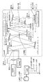
図1に従い、その構成を説明すると、露光光源は励起用パルスレーザーであり、この光源は集光レンズ、プラズマターゲット供給装置からなり、EUV光を供給する。照明光学系はミラー、オプティカルインテグレータ、EUV光を円弧状に整形する画角制限アパーチャからなり、励起用パルスレーザーから照射されたレーザーを成形してレチクルを均一に照明する。投影光学系は複数枚のミラーにより構成され、レチクルパターンを縮小してウエハに転写する。この時レチクルステージとウエハステージはそれぞれ投影光学系の縮小比に従い同期走査する。
【0054】
露光装置はステップ・アンド・スキャンを繰り返して露光を行い、ウエハ全面に露光が完了すると、次のウエハへと移る。さらに全てのウエハへの露光が終了すると、レチクルを交換し、再び同様の手順で露光を繰り返す。ステップ・アンド・スキャン時、ウエハ交換時、レチクル交換時など各行程に応じて、例えば前ショットと次ショットとの間隔などの入射条件が異なる。そのため安定した露光を行なうには、入射条件に応じて、露光光の照射毎に生じる発熱によるミラーの形状変化を安定化させることが必要となる。ミラー形状安定化はミラー温度を入射条件に応じ制御することで行なう。すなわち、ミラー形状を安定させるために、どのようにミラーの温度制御を行う温度調節機構の温度を変化させるか予め求めておくことが必要となる。
【0055】
この温度変化とミラー形状の安定化を図るために、露光装置を実際の装置と同様の露光条件のもとで動作させて、ミラーに実際の露光光と同様の強度および時間間隔で光を照射し、その際、温度変化により生じるミラー形状の変化を測定しながら、形状変化の誤差と温度の関係を求め、形状を一定にするために必要な温度調節機構の最適な制御則を求める。
【0056】
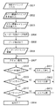
この制御の方法の一例を図2のフローチャートおよび図4から図7を用い説明する。
【0057】
ミラー形状が入射光の強度Pと入射時間t0、温度調節機構の温度制御エネルギP'とその温度制御の開始時間と入射開始の時間との時間差Δt'で表される場合について説明する。この場合はミラーの形状誤差を最小にする温度調節機構の制御パラメータを(P',Δt')とし、そのパラメータを入射条件(P, t0)のパラメータにより表すことにより、制御量を決定する。
【0058】
まず、図2のステップS200において、露光仕様の範囲で入射光の強度Pと露光タイミングt0を決定する(図4中の上段のパルス列)。続いて時間差Δt'を選択し(S210)、この時間差Δt'を固定したまま温度調節機構の温度制御エネルギP'を変化させながら干渉計でミラーの形状誤差を測定し(S220)、そのΔt'に対してミラーの形状誤差が最小となる温度制御エネルギP'を求める(S230:図5中のB-1が誤差の分布の最小となる点を示す)。ステップS230の処理により、所定のΔt'に対して、ミラー形状誤差が最小となる温度条件P'が求められることになる。Δt'を変化させて同様な測定を行い(S240)、ある入射条件で最適な温度制御エネルギP'を求めていく。続いて入射条件を変化させふたたび同様の手順を繰り返して測定を行う(S250)。そして、Δt'に対して、十分なデータが揃い、仕様上の入射条件(S200)に対して十分なデータが揃った段階でデータ取得は完了する(S260)。
【0059】
以上の処理工程により得られたデータは、参照テーブルデータとして、図1の制御データ管理データベースに格納管理することができる。
【0060】
また、得られたデータからミラー形状を最適にする(P',Δt')を入射条件(P, t0)の多項式で近似して表してもよいし、温度制御の開始時間と入射開始の時間との時間差Δt'を図6のようにΔt'=0.1sec,0.3sec,0.5secと変化させた場合の入射光の強度Pと温度調節機構の温度制御エネルギP'の関係を参照テーブルデータとして管理し、その変化の状態を図6のようにグラフ化してもよい。
【0061】
図2のフローチャートは、時間差Δt'を固定して、温度調節機構の温度P'を変化させながらミラー形状を最適にする条件を求める処理の流れを示すものであるが、条件の決定プロセスは、この手順に限るものではなく、図3のフローチャートのように、先に、温度制御エネルギの条件P'を選択して(S310)、時間差Δt'を変化させながらミラーの形状誤差を測定し(S320)、ミラーの形状誤差が最小となるΔt'を求める(S330)方法でもよい。
【0062】
そして、温度調節機構の温度P'に対して、十分なデータが揃い、仕様上の入射条件(S300)に対して十分なデータが揃った段階でデータ取得は完了する(S360)。
【0063】
以上の処理工程により得られたデータは、参照テーブルデータとして、図1の制御データ管理データベースに格納管理することができる。
【0064】
また、得られたデータからミラー形状を最適にする(P',Δt')を入射条件(P, t0)の多項式で近似して表してもよいし、温度調節機構の温度制御エネルギP'を図7のように温度制御エネルギの条件をP'=0.1W,0.3W,0.5Wと変化させた場合のΔt'とt0の関係を参照テーブルデータとして管理し、その変化の状態を図7のようにグラフ化してもよい。
【0065】
いずれの場合にせよ測定点が増えるほど形状制御の精度は向上する。
【0066】
以上の例では入射条件をパラメータ(P, t0)で表し、温度調節機構の制御パラメータを(P',Δt')としたが、パラメータはこの4つに限定されるものではない。パラメータ数を増やした場合も各パラメータを変化させながらミラーの形状誤差を最小にする温度調節機構の制御パラメータを求めていけばよい。パラメータ数が増えるほどミラーの形状制御の精度は向上する。この多項式および変化表を求める一連の作業は露光機一台ずつに対して行ってもよいし、同じ仕様を持つ複数の露光機から任意に一台を抜き出して行ってもよい。
【0067】
実際の露光では上記の多項式もしくは変化表に基づき、温度調節機構の動作を決める。従って、露光条件に関わらず、実際に配置された場合のミラー形状が一定となり、安定な露光が可能となる。つまり、ミラー形状が一定となるように積極的にミラー温度を変えることで安定な露光を実現することが可能となる。
【0068】
また、露光機内に干渉計を備え、ミラー形状を常時測定する場合は、ミラー形状と温度調節機構との関係を予め求めて、制御データ管理データベースに格納管理する。露光中にミラー形状を測定し、この制御データ管理データベースに基づき、温度調節機構を動かすことでミラー形状を一定に保つことができる。
【0069】
また、ミラー形状を常時測定して形状を最適化するために動かした温度調節機構のデータを露光ごとに蓄積しておけば、このデータを温度調節機構の予め決められている動作に組み込むことで次回からの露光をさらに最適化することもできる。
【0070】
以上の説明において、干渉計を用いてミラー形状を測定するとしたが、ミラーのつくる像点とミラー形状との関係式が求まっている場合は像点からミラー形状を判断してもよい。
【0071】
次に、ミラーおよびミラー保持部周辺の温度調節機構の構成を、図9を用い説明する。ミラー保持部4の内部には温度調節のための冷却水路5が設けられており、この内部を冷却水が循環してミラー3の温度を制御する構成となっている。冷却水の温度は冷却水路5の上流に備えられたヒーター7により温度調節がなされる。ヒーター電源6の電力はタイミング制御系1からの信号により、温度制御系2を介して制御される。
【0072】
ここで、ミラー形状とヒーター電力(温度の調節)の関係を事前に求めておく。ヒーター7の温度制御が可能な範囲でヒーター7を動かし、冷却水の温度を変えて、その時の温度によるミラー形状の測定を繰り返し行い、ミラー形状と冷却温度との関係のデータを収集し、得られたデータを温度制御系2に入力する。このデータは常時得られる干渉計により収集され、ミラー形状を温度変化に拠らず、一定に保つために利用される。
【0073】
尚、ミラー形状とヒーター電力(温度の調節)の関係は図2及び図3のフローチャートの説明で示した手順により定めることができる。
【0074】
以上述べた温度制御データの取得から露光までの露光装置の動作を図8のフローチャートに示す。露光装置の全体的な動作は、タイミング制御系1により実行され、このタイミング制御系1は光源、レチクルステージ、ウエハステージ、温度制御系の各動作タイミングを制御する。光源のパルスレーザーに関しては露光開始および露光終了の信号が送られる(S801)。ウエハステージにはスキャンの開始および終了のタイミングが入力され(S802)、レチクルステージにはスキャンの開始および終了のタイミングが入力される(S803)。
【0075】
ステップS801からS803において、光源、レチクルステージ、ウエハステージの各タイミング制御量が入力された時点でミラーに照射される露光光の強度と時間の関係が決まる。露光光の強度と時間の関係が決まると、ステップS804において、タイミング制御系1は温度制御系2に送るための制御データを取得する。
【0076】
先に説明したように、ミラー形状が入射光の強度Pと入射時間t0、温度調節機構の温度制御エネルギP'とその開始時間と入射開始の時間との時間差Δt'、で表されると仮定すると、この場合、入射光の強度Pと入射時間t0は光源のパルスレーザーの強度とその発振時間である。温度調節機構の温度制御エネルギP'は冷却水路に設けられたヒーター温度に基づくものであり、その冷却開始時間と入射開始の時間との時間差Δt'は、ヒーター電源の温度調節を開始する時間とレーザー発振を開始する時間との差に対応する。そして、これらの関係を図2、図3で示したフローチャートに従い、光源であるパルスレーザーのパラメータを変化させながらミラー形状を最適とする条件(P',Δt')を求め、ヒーター7を制御するためのデータを求める。
【0077】
このデータは、露光装置が動作するタイミング、すなわち露光光の照射に起因してミラーの発熱により生じる形状の変化を安定化させるための温度制御系の制御データであり、種々の条件に応じて、形状誤差を最小にするデータが求められる(S805)。
【0078】
ステップS805で求められたデータは、タイミング制御系1に入力され、温度制御系2を介してヒータータイミング制御が実行される(S806)。
【0079】
ヒータータイミング制御により、ヒーター電源6が駆動して、ヒーター7が制御されることにより、冷却水に所定の熱量が与えられる。ミラー保持部4に保持されたミラー3の温度は、冷却水による熱量の授受により安定化され、温度変化による形状変化の発生は抑制される。
【0080】
ステップS807でスキャン露光が開始され、ウエハ全面が終了したか否か判断し(S808)、終了していなければ次の走査露光開始位置への移動し(S811)、ウエハについて露光が終了した場合は、ウエハ交換の信号が送られる(S809-No、S812)。露光開始および終了のタイミングはそれぞれのステージのスキャン開始(S807)および終了(S814)と一致し、ウエハの交換はウエハ全面に転写が完了した時点で、レチクル(マスク)の交換(S810−No、S813)は所定の枚数のウエハが完了した時点で行われる。
【0081】
ステップS806におけるヒータータイミング制御と、露光動作の詳細を以下に説明する。
【0082】
タイミング制御系1は、ステップS804、S805で取得したヒーター制御データに基づき、温度制御系2を介してヒーター電源6を制御する。この制御において、ヒーター7を動作させて、規定の時間が経過した時点で、すなわちミラーが規定の形状に安定化した時点でパルスレーザーに発振開始の信号が送られ露光が開始される。同時にレチクルステージ、ウエハステージにスキャン開始の信号が送られレチクルパターンの転写が始まる。
【0083】
一回のスキャン露光が終了するとパルスレーザーには発振終了の信号が送られ露光が終了する。温度制御系2は露光中およびウエハステージが次の走査露光開始位置に移動する間も、予めタイミング制御系に入力されたデータに従い、ミラー形状が一定になるようにヒーター電源6を調節してミラー温度を変化させる。露光装置はステップ・アンド・スキャンを繰り返し、ウエハ全面の転写が完了した時点でウエハ交換となる。このタイミングもウエハステージに送られる予め入力されたタイミング制御系からの信号に基づいて行われる。ウエハ交換に必要な時間はステップ・アンド・スキャンの時間間隔と異なるが、その間もヒーター電源は予め測定されたデータをもとに制御されるのでミラー形状は一定に保たれる。所定の枚数のウエハへの転写が完了した時点でレチクルの交換が行われるが、ここでもミラー形状が一定となるようにミラー温度が制御される。
【0084】
ミラー3の形状は常時干渉計により測定され、タイミング制御系1に入力されたデータに従いヒーター電力を調節し、形状が一定とならない場合は、干渉計からのミラー形状情報に基づき、予め求めたミラー形状とヒーター電力の関係に従い温度制御系2が電力を調節する。温度制御系2の動作のタイミングと形状変化量の情報はタイミング制御系1に入力されタイミング制御系の情報は更新される。次回露光時にはこの更新された情報に従い露光することができる。
【0085】
データの更新が進むに従い、ミラー形状の精度は向上する。十分な回数のデータ更新の後では、タイミング制御系の情報は理想的な値に漸近しており、タイミング制御系1に入力されたデータに従いヒーター電力を調節することで形状が一定となる。このため、タイミング制御系の情報が理想的な値に漸近した以降の露光では干渉計によるミラー形状の測定は必要なくなる。また、同一の仕様を持つ露光機であれば、この十分な回数の更新が行なわれたデータを用いることで、干渉計による形状計測を行なわなくても安定な露光を行なうことができる。
【0086】
このように冷却水温度を露光条件およびミラー形状に応じて変化させることでミラー形状を一定に保つことができ、結果として安定な露光が可能となる。
【0087】
なお本実施形態ではヒーター出力のパラメータを励起用レーザーのパラメータとして多項式および変化表を求めたが、ウエハ上で観測されるEUV光の強度をパラメータとしてもよい。この場合、多項式および変化表を作成するためのデータを取得する際にウエハ上に光強度センサを設け、そこで検知されるEUV光の強度とタイミングをパラメータとして用いる。
【0088】
前述の入射光の強度Pと入射時間t0に対応するのはそれぞれウエハ上のセンサが検知するEUV光の強度とその時間である。さらに、上記例ではヒーター出力のパラメータを励起用レーザーのパラメータとして多項式および変化表を求めたが、ヒーターより下流に位置する冷却水温度とその時間変化をパラメータとしてもよい。この場合、ヒーターより下流に温度計を設置し、そこで検知される冷却水の温度とタイミングをパラメータとして用いる。温度計はヒーター電源と電気的につながっており、冷却水温度を計測しながらヒーターの電力を制御する。前述の温度調節機構の温度制御エネルギP'と時間差Δt'に対応するのは温度計により検出される冷却水温度とそのタイミングに対応する。
【0089】
本実施形態によれば、光学素子の温度変動に起因する反射面形状の変化による解像度の低下やコントラストの低下などが起こらず、安定して微細なパターンの転写ができる露光装置を提供することができる。
【0090】
<第2実施形態>
第2実施形態が第1実施形態と異なるのは、冷却水の温度調節機構として、図10に示すように異なる水温をもつ二系統(10a,10b)の冷却水とその二系統の冷却水の個々の流量を調節するためのバルブ8を備えた機構を用いることである。
【0091】
タイミング制御系1は温度制御系2と接続し、それぞれの系統の冷却水を温度制御する。温度制御系2は、第1系統の冷却水10aと第2系統の冷却水10bとをそれぞれ温度制御するためのヒーター電源6a,6bとヒーター7a,7bとを制御する。更に、温度制御系2は、バルブ8の開閉角度を制御する。バルブ8の開閉角度を制御することで、第1系統に流れる冷却水と第2系統に流れる冷却水とを所定の流量の割合に制御できるので、流量割合に基づき、温度の切り替えを迅速にすることができる。
【0092】
バルブ8の制御により所定の流量割合に制御された冷却水は冷却水路5に流入し、ミラー3を保持するミラー保持部4を介してミラー3の裏面を冷却する。
【0093】
温度制御系2のバルブ制御のタイミングは第1実施形態と同様、タイミング制御系により予め測定されたデータをもとにミラー形状が一定になるように制御される。
【0094】
本実施形態によれば、冷却温度の切り替えを迅速に行なうことが可能となり、光学素子の温度変動に起因する反射面形状の変化を迅速に抑制することが可能となる。
【0095】
<第3実施形態>
第3実施形態が第1実施形態と異なるのは、ミラーの温度調節機構として、図11に示すようにミラー3とミラー保持部4との間にペルチエ素子9を備えることである。ペルチエ素子9はペルチエ素子電源10を介してタイミング制御系1に電気的に接続されており、ぺルチエ素子9に流れる電流に応じてミラー3を加熱または吸熱により冷却する。ペルチエ素子9の裏側(ミラー冷却部4)に冷却水を流すのはペルチエ素子9がミラー3から吸収する熱を放熱するためである。タイミング制御系1によりペルチエ素子に電流が流され、そのタイミングは上記第1実施形態と同様、タイミング制御系1により予め測定されたデータをもとにミラー形状が一定になるように制御される。
【0096】
ぺルチエ素子9を介在することにより、タイミング制御系1からの指示に対して、温度の急峻な変化に対応した、応答性(追従性)の高い冷却性能を実現することが可能となる。
【0097】
更に、上記の実施形態において冷却水の循環により生じる振動がミラー位置や形状へ影響を及ぼす場合は、その振動の伝達を緩衝して、ミラー3と保持部の間に熱を運ぶ機構、例えばヒートパイプ12などを備えることで解決できる。図12にその構成を示す。ヒートパイプ12はミラー3の熱を冷却部4まで運ぶ機能を持ち、ミラー3に直接、もしくはミラー裏面に取り付けられた熱伝導のよい金属板11などを介して取り付けられる。ヒートパイプにはベローズなど振動を吸収する制振機構が備えられる場合もある。またヒートパイプ12は複数備えられていてもよいし、一本だけでもよい。
【0098】
本発明はパルスレーザーの発振により露光を開始する装置に関し説明してきたが、これに限定されず、露光の開始、終了を照明系の一部に備えられたシャッターの開閉を用いて露光するタイプの露光装置にも適用できる。
【0099】
また温度調節機構として冷却水、ペルチエ素子を用いる実施例を挙げたが温度調節機構はこれらに限定されるものではない。
【0100】
本実施形態によれば、冷却水の循環による冷却に加え、ぺルチエ素子を介在させることにより、温度の急峻な変化に対応した、応答性(追従性)の高い冷却性能を実現することが可能となる。また、冷却水の循環による振動の影響を排除することが可能となる。
【0101】
<半導体生産システムの実施形態>
次に、上記露光装置を用いた半導体デバイス(ICやLSI等の半導体チップ、液晶パネル、CCD、薄膜磁気ヘッド、マイクロマシン等)の生産システムの例を説明する。これは半導体製造工場に設置された製造装置のトラブル対応や定期メンテナンス、あるいはソフトウェア提供などの保守サービスを、製造工場外のコンピュータネットワークを利用して行うものである。
【0102】
図14は全体システムをある側面から切り出して表現したものである。図中、1010は半導体デバイスの製造装置を提供するベンダー(装置供給メーカー)の事業所である。製造装置の実例として、半導体製造工場で使用する各種プロセス用の半導体製造装置、例えば、前工程用機器(露光装置、レジスト処理装置、エッチング装置等のリソグラフィー装置、熱処理装置、成膜装置、平坦化装置等)や後工程用機器(組立て装置、検査装置等)を想定している。事業所1010内には、製造装置の保守データベースを提供するホスト管理システム1080、複数の操作端末コンピュータ1100、これらを結ぶんでイントラネットを構築するローカルエリアネットワーク(LAN)1090を備える。ホスト管理システム1080は、LAN1090を事業所の外部ネットワークであるインターネット1050に接続するためのゲートウェイと、外部からのアクセスを制限するセキュリティ機能を備える。
【0103】
一方、1020〜1040は、製造装置のユーザーとしての半導体製造メーカーの製造工場である。製造工場1020〜1040は、互いに異なるメーカーに属する工場であっても良いし、同一のメーカーに属する工場(例えば、前工程用の工場、後工程用の工場等)であっても良い。各工場1020〜1040内には、夫々、複数の製造装置1060と、それらを結んでイントラネットを構築するローカルエリアネットワーク(LAN)1110と、各製造装置1060の稼動状況を監視する監視装置としてホスト管理システム1070とが設けられている。
【0104】
各工場1020〜1040に設けられたホスト管理システム1070は、各工場内のLAN1110を工場の外部ネットワークであるインターネット1050に接続するためのゲートウェイを備える。これにより各工場のLAN1110からインターネット1050を介してベンダー1010側のホスト管理システム1080にアクセスが可能となる。ここで、典型的には、ホスト管理システム1080のセキュリティ機能によって、限られたユーザーだけがホスト管理システム1080に対するアクセスが許可される。
【0105】
このシステムでは、インターネット1050を介して、各製造装置1060の稼動状況を示すステータス情報(例えば、トラブルが発生した製造装置の症状)を工場側からベンダー側に通知し、その通知に対応する応答情報(例えば、トラブルに対する対処方法を指示する情報、対処用のソフトウェアやデータ)や、最新のソフトウェア、ヘルプ情報などの保守情報をベンダー側から工場側に送信することができる。各工場1020〜1040とベンダー1010との間のデータ通信および各工場内のLAN1110でのデータ通信には、典型的には、インターネットで一般的に使用されている通信プロトコル(TCP/IP)が使用される。
【0106】
なお、工場外の外部ネットワークとしてインターネットを利用する代わりに、第三者がアクセスすることができない、セキュリティの高い専用線ネットワーク(ISDNなど)を利用することもできる。また、ホスト管理システムはベンダーが提供するものに限らずユーザーがデータベースを構築して外部ネットワーク上に置き、ユーザーの複数の工場から該データベースへのアクセスを許可するようにしてもよい。
【0107】
さて、図15は本実施形態の全体システムを図14とは別の側面から切り出して表現した概念図である。先の例ではそれぞれが製造装置を備えた複数のユーザー工場と、該製造装置のベンダーの管理システムとを外部ネットワークで接続して、該外部ネットワークを介して各工場の生産管理や少なくとも1台の製造装置の情報をデータ通信するものであった。これに対し本例は、複数のベンダーの複数の製造装置を備えた工場と、該複数の製造装置のそれぞれのベンダーの管理システムとを工場外の外部ネットワークで接続して、各製造装置の保守情報をデータ通信するものである。図中、2010は製造装置ユーザー(半導体デバイス製造メーカー)の製造工場であり、工場の製造ラインには各種プロセスを行う製造装置、ここでは例として露光装置2020、レジスト処理装置2030、成膜処理装置2040が導入されている。
【0108】
なお、図14では製造工場2010は1つだけ描いているが、実際は複数の工場が同様にネットワーク化されている。工場内の各装置はLAN2060で接続されてイントラネットを構成し、ホスト管理システム2050で製造ラインの稼動管理がされている。一方、露光装置メーカー2100、レジスト処理装置メーカー2200、成膜装置メーカー2300などベンダー(装置供給メーカー)の各事業所には、それぞれ供給した機器の遠隔保守を行なうためのホスト管理システム2110,2210,2310を備え、これらは上述したように保守データベースと外部ネットワークのゲートウェイを備える。ユーザーの製造工場内の各装置を管理するホスト管理システム2050と、各装置のベンダーの管理システム2110, 2210, 2310とは、外部ネットワーク2000であるインターネットもしくは専用線ネットワークによって接続されている。このシステムにおいて、製造ラインの一連の製造機器の中のどれかにトラブルが起きると、製造ラインの稼動が休止してしまうが、トラブルが起きた機器のベンダーからインターネット2000を介した遠隔保守を受けることで迅速な対応が可能で、製造ラインの休止を最小限に抑えることができる。
【0109】
半導体製造工場に設置された各製造装置はそれぞれ、ディスプレイと、ネットワークインターフェースと、記憶装置にストアされたネットワークアクセス用ソフトウェアならびに装置動作用のソフトウェアを実行するコンピュータを備える。記憶装置としては内蔵メモリやハードディスク、あるいはネットワークファイルサーバーなどである。上記ネットワークアクセス用ソフトウェアは、専用又は汎用のウェブブラウザを含み、例えば図16に一例を示す様な画面のユーザーインターフェースをディスプレイ上に提供する。各工場で製造装置を管理するオペレータは、画面を参照しながら、製造装置の機種(4010)、シリアルナンバー(4020)、トラブルの件名(4030)、発生日(4040)、緊急度(4050)、症状(4060)、対処法(4070)、経過(4080)等の情報を画面上の入力項目に入力する。入力された情報はインターネットを介して保守データベースに送信され、その結果の適切な保守情報が保守データベースから返信されディスプレイ上に提示される。またウェブブラウザが提供するユーザーインターフェースはさらに図示のごとくハイパーリンク機能(4100〜4120)を実現し、オペレータは各項目の更に詳細な情報にアクセスしたり、ベンダーが提供するソフトウェアライブラリから製造装置に使用する最新バージョンのソフトウェアを引出したり、工場のオペレータの参考に供する操作ガイド(ヘルプ情報)を引出したりすることができる。
【0110】
次に上記説明した生産システムを利用した半導体デバイスの製造プロセスを説明する。図17は半導体デバイスの全体的な製造プロセスのフローを示す。ステップ1(回路設計)では半導体デバイスの回路設計を行なう。ステップ2(露光制御データ作製)では設計した回路パターンに基づいて露光装置の露光制御データを作製する。一方、ステップ3(ウエハ製造)ではシリコン等の材料を用いてウエハを製造する。ステップ4(ウエハプロセス)は前工程と呼ばれ、上記用意したマスクとウエハを用いて、リソグラフィー技術によってウエハ上に実際の回路を形成する。次のステップ5(組み立て)は後工程と呼ばれ、ステップ4によって作製されたウエハを用いて半導体チップ化する工程であり、アッセンブリ工程(ダイシング、ボンディング)、パッケージング工程(チップ封入)等の組立て工程を含む。ステップ6(検査)ではステップ5で作製された半導体デバイスの動作確認テスト、耐久性テスト等の検査を行なう。こうした工程を経て半導体デバイスが完成し、これを出荷(ステップ7)する。例えば、前工程と後工程はそれぞれ専用の別の工場で行われてもよく、この場合、これらの工場毎に上記説明した遠隔保守システムによって保守がなされる。また前工程工場と後工程工場との間でも、インターネットまたは専用線ネットワークを介して生産管理や装置保守のための情報がデータ通信されてもよい。
【0111】
図17は上記ウエハプロセスの詳細なフローを示す。ステップ11(酸化)ではウエハの表面を酸化させる。ステップ12(CVD)ではウエハ表面に絶縁膜を成膜する。ステップ13(電極形成)ではウエハ上に電極を蒸着によって形成する。ステップ14(イオン打込み)ではウエハにイオンを打ち込む。ステップ15(レジスト処理)ではウエハに感光剤を塗布する。ステップ16(露光)では上記説明した露光装置によって回路パターンをウエハに描画(露光)する。ステップ17(現像)では露光したウエハを現像する。ステップ18(エッチング)では現像したレジスト像以外の部分を削り取る。ステップ19(レジスト剥離)ではエッチングが済んで不要となったレジストを取り除く。これらのステップを繰り返し行なうことによって、ウエハ上に多重に回路パターンを形成する。各工程で使用する製造機器は上記説明した遠隔保守システムによって保守がなされているので、トラブルを未然に防ぐと共に、もしトラブルが発生しても迅速な復旧が可能で、従来に比べて半導体デバイスの生産性を向上させることができる。
【0112】
【発明の効果】
以上述べたように本発明によれば、露光条件によってミラー(反射面)形状変化を簡易に制御することができ、安定した精度において露光が可能となる。
【0113】
本発明によれば、光学素子の温度変動等に起因する反射面形状の変化による解像度の低下やコントラストの低下などを適切に防止し、安定して微細なパターンの転写ができる露光装置およびその露光装置を用いた半導体デバイスの製造方法を提供することができる。
【図面の簡単な説明】
【図1】本発明にかかる露光装置の構成を説明する図である。
【図2】ミラー形状を最適化するために必要な温度調節機構の制御を求めるためのフローチャートである。
【図3】ミラー形状を最適化するために必要な温度調節機構の制御を求めるためのフローチャートである。
【図4】ミラーに照射される入射光の強度の時間変化と温度調節機構の制御の時間変化の関係を説明する図である。
【図5】温度調節機構の出力に対し、ミラーの形状誤差を測定を例示的に説明する図である。
【図6】図5で示されるミラー形状誤差が最小となる点を各露光条件のもとでプロットしたものを説明する図である。
【図7】図3のフローチャートに従って、ミラー形状が最小となる点を各露光条件のもとでプロットしたものを説明する図である。
【図8】温度制御データの取得から露光までの処理の流れを説明するフローチャートである。
【図9】本発明にかかる第1実施形態で、ミラー及びミラー冷却部の構成を説明する図ある。
【図10】本発明にかかる第2実施形態で、ミラー及びミラー冷却部の構成を説明する図ある。
【図11】本発明にかかる第3実施形態で、ミラー及びミラー冷却部の構成を説明する図ある。
【図12】ミラー冷却部がミラーに及ぼす振動の効果を軽減するためにヒートパイプを備えた構成を説明する図である。
【図13】従来のEUV光を用いた露光装置の構成を説明する図である。
【図14】本発明の一実施形態に係る露光装置を含む半導体デバイスの生産システムをある角度から見た概念図である。
【図15】本発明の一実施形態に係る露光装置を含む半導体デバイスの生産システムを別の角度から見た概念図である。
【図16】本発明の一実施形態に係る露光装置を含む半導体デバイスの生産システムにおけるユーザインタフェースの具体例を示す図である。
【図17】本発明の一実施形態に係る露光装置によるデバイスの製造プロセスのフローを説明する図である。
【図18】本発明の一実施形態に係る露光装置によるウエハプロセスを説明する図である。[0001]
BACKGROUND OF THE INVENTION
The present invention relates to a mirror device for transferring a fine circuit pattern, a mirror adjustment method, an exposure apparatus, an exposure method, a semiconductor device manufacturing method using the exposure apparatus, and the like.
[0002]
[Prior art]
Conventionally, reduction projection exposure using ultraviolet rays has been performed as a printing (lithography) method for manufacturing fine semiconductor elements such as semiconductor memories and logic circuits. The minimum dimension that can be transferred by this reduced projection exposure is proportional to the wavelength of light used for transfer and inversely proportional to the numerical aperture of the projection optical system. For this reason, the wavelength of light used for transferring fine circuit patterns has been shortened, and ultraviolet light used for mercury lamp i-line (wavelength 365 nm), KrF excimer laser (wavelength 248 nm), and ArF excimer laser (wavelength 193 nm). The wavelength of light has become shorter.
[0003]
However, semiconductor elements have been miniaturized rapidly, and lithography using ultraviolet light has been limited in microfabrication for manufacturing semiconductor elements. Therefore, in order to efficiently burn a very fine circuit pattern whose semiconductor device line width is less than 0.1 μm, extreme ultraviolet light (hereinafter referred to as “EUV light”) having a wavelength of about 10 to 15 nm, which is shorter than ultraviolet light. )) Has been developed.
[0004]
In the EUV light region, the absorption of light by substances becomes very large, so it is not practical to use a lens optical system that utilizes the refraction of light such as that used in visible light and ultraviolet light, and EUV light was used. In the exposure apparatus, a reflection optical system is used. In this case, a reticle that is an original plate is also a reflective reticle in which a pattern to be transferred is formed on a mirror by a light absorber.
[0005]
As a reflection type optical element adopted in an exposure apparatus using EUV light, there are a multilayer mirror and a grazing incidence total reflection mirror. Since the real part of the refractive index is slightly smaller than 1 in the EUV region, total reflection occurs when used in an oblique incidence state where EUV light is incident on the surface. Usually, a high reflectance of several tens% or more is obtained at an oblique incidence within several degrees as measured from the surface to be irradiated. However, the degree of freedom in optical design is small, and it is difficult to use a total reflection mirror for a projection optical system.
[0006]
As a mirror for EUV light used at an incident angle close to normal incidence, a multilayer mirror in which two kinds of substances having different optical constants are alternately stacked is used. Molybdenum and silicon are alternately laminated on the surface of a glass substrate polished to a precise surface shape. For example, the thickness of the layer is about 0.2 nm for the molybdenum layer, about 0.5 nm for the silicon layer, and about 20 layers. A value obtained by adding the thicknesses of the two kinds of substances is called a film cycle. In the above example, the film period is the thickness of the molybdenum layer (0.2 nm) + the thickness of the silicon layer (0.5 nm) = the film period (0.7 nm).
[0007]
When EUV light is incident on such a multilayer mirror, EUV light having a specific wavelength is reflected. Here, Bragg's equation (1) can be approximated by assuming that the incident angle of light incident on the multilayer mirror is θ, the wavelength of the EUV light is λ, and the film period is d.
2 × d × sin θ = λ (1)
Only EUV light with a narrow bandwidth centered around λ that satisfies this relationship is efficiently reflected. The bandwidth at this time is about 0.6 to 1 nm.
[0008]
The reflectivity of the reflected EUV light is about 0.7 at the maximum, and the EUV light that is not reflected is absorbed in the multilayer film or the substrate, and most of the energy becomes heat. Multilayer mirrors have a greater light loss than visible light mirrors, so it is necessary to minimize the number of mirrors. In order to realize a wide exposure area with a small number of mirrors, only a thin arc-shaped area (ring field) separated by a certain distance from the optical axis is used to simultaneously scan the reticle and wafer to transfer a large area. A method (scan exposure) is performed.
[0009]
In scan exposure, reduction projection exposure equipment using EUV light mainly consists of an EUV light source, illumination optical system, reflective reticle, projection optical system, reticle stage, wafer stage, alignment optical system, vacuum system, etc. Is done.
[0010]
For example, a laser plasma light source is used as the EUV light source. In this method, a target material placed in a vacuum vessel is irradiated with high-intensity pulsed laser light to generate high-temperature plasma, and EUV light with a wavelength of, for example, about 13 nm is used. As the target material, a metal thin film, an inert gas, a droplet, or the like is used, and is supplied into the vacuum container by means such as a gas jet. In order to increase the average intensity of the emitted EUV light, the repetition frequency of the pulse laser should be high, and it is usually operated at a repetition frequency of several kHz.
[0011]
The illumination optical system includes a plurality of multilayer films or oblique incidence mirrors, an optical integrator, and the like. The first stage collector mirror collects EUV light that is emitted almost isotropically from the laser plasma. The optical integrator has a role of uniformly illuminating the mask with a predetermined numerical aperture. In addition, an aperture for limiting an area illuminated by the reticle surface to an arc shape is provided at a position conjugate with the reticle of the illumination optical system.
[0012]
The projection optical system is composed of a plurality of mirrors. When the number of mirrors constituting the projection optical system is small, the use efficiency of EUV light is high, but aberration correction becomes difficult. The number of mirrors necessary for aberration correction is about 4 to 6. The shape of the reflecting surface of the mirror is a convex or concave spherical or aspherical surface. In this case, the numerical aperture NA is about 0.1 to 0.2. The mirror is made of a material such as low-expansion glass or silicon carbide that has high rigidity, high hardness, and low thermal expansion, and then grinds and polishes it to form a predetermined reflective surface shape. A multilayer film such as is formed. If the incident angle is not constant depending on the location in the mirror plane, as is clear from the Bragg equation described above, the multilayer film with a constant film period has a higher reflectivity depending on the location, and therefore the wavelength of the EUV light shifts. . Therefore, it is necessary to have a film period distribution so that EUV light having the same wavelength is efficiently reflected in the mirror plane.
[0013]
The reticle stage and wafer stage have a mechanism that scans synchronously at a speed ratio proportional to the reduction magnification. Here, the scanning direction within the reticle or wafer surface is taken as the X axis, the direction perpendicular to the scanning direction is taken as the Y axis, and the direction perpendicular to the reticle or wafer surface is taken as the Z axis.
[0014]
The reticle is held by a reticle chuck on the reticle stage. The reticle stage has a drive mechanism for moving at high speed in the X-axis direction. In addition, a fine movement mechanism is provided in the X-axis direction, the Y-axis direction, the Z-axis direction, and the rotation direction around each axis so that the reticle can be positioned. The position and orientation of the reticle stage are measured by a laser interferometer, and the position and orientation are controlled based on the result.
[0015]
The wafer is held on the wafer stage by a wafer chuck. Similar to the reticle stage, the wafer stage has a mechanism that moves at high speed in the X-axis direction. In addition, a fine movement mechanism is provided in the X-axis direction, the Y-axis direction, the Z-axis direction, and the rotation direction around each axis so that wafer positioning can be performed. The position and orientation of the wafer stage are measured by a laser interferometer, and the position and orientation are controlled based on the result.
[0016]
The alignment detection mechanism measures the positional relationship between the reticle position and the optical axis of the projection optical system, and the positional relationship between the wafer position and the optical axis of the projection optical system, and the projected image of the reticle matches the predetermined position on the wafer. Thus, the position and angle of the reticle stage and wafer stage are set.
[0017]
Also, the focus position in the Z-axis direction is measured on the wafer surface by the focus position detection mechanism, and by controlling the position and angle of the wafer stage, the imaging position of the wafer surface is always relative to the projection optical system during exposure. Kept.
[0018]
When one scan exposure is completed on the wafer, the wafer stage is stepped in the X and Y directions and moved to the next scan exposure start position, and the reticle stage and wafer stage are again proportional to the reduction magnification of the projection optical system. The synchronous scanning is performed in the X direction at the speed ratio. In this manner, the operation of synchronously scanning the reduced projection image of the reticle while it is formed on the wafer is repeated (step-and-scan). Thus, the reticle transfer pattern is transferred onto the entire wafer surface.
[0019]
[Means for Solving the Problems]
However, the conventional EUV exposure apparatus has the following problems.
[0020]
As described above, the reflectance of EUV light reflected by the multilayer mirror is about 0.7 at maximum, and the unreflected light is absorbed in the multilayer film or the substrate, and most of the energy becomes heat. . For this reason, when EUV light is irradiated onto a mirror, reticle, etc., the light that has not been reflected is absorbed by the optical element and generates heat.
[0021]
EUV light as exposure light is strongly absorbed by the gas. For example, if EUV light with a wavelength of 13 nm propagates 1 m in a space filled with 10 Pa of air, about 50% of it is absorbed. In order to avoid absorption by gas, the space where EUV light propagates is at least 10-1Pa or less, preferably 10-3It is necessary to keep the pressure below Pa.
[0022]
Also, when molecules containing carbon such as hydrocarbons remain in the space where the optical element irradiated with EUV light is placed, carbon gradually adheres to the optical element surface due to light irradiation, and this absorbs EUV light. Therefore, there is a problem that the reflectance is lowered, and in order to prevent this carbon adhesion, the space where the optical element irradiated with EUV light is placed is at least 10-FourPa or less, preferably 10-6It is necessary to keep the pressure below Pa.
[0023]
For this reason, the EUV optical element cannot be cooled by heat conduction to the surrounding gas, and must be cooled through a mirror holder or a reticle chuck that holds the optical element. Therefore, the mirror and reticle are fixed to a mirror holder and reticle chuck provided with cooling means such as circulating cooling water at a constant temperature, and the heat generated by absorption of EUV light is carried away from the optical element to the outside. The temperature rise is controlled.
[0024]
The optical element is irradiated with EUV light only during exposure, and during other times, for example, while the wafer stage moves to the next scanning exposure start position, during reticle replacement, or during wafer replacement, There is no energy absorption because there is no irradiation. That is, the energy applied to the optical element is not constant in time, and varies greatly with time. For this reason, a cooling method that does not take into account temporal changes in the amount of heat absorbed by the optical element, such as circulating cooling water at a constant temperature through a mirror holder or reticle chuck that holds the optical element, can maintain the optical element at a constant temperature. It is difficult, and it is difficult to avoid a change in the shape of the reflecting surface due to a temperature change of the optical element before and during the exposure.
[0025]
Furthermore, even if the temperature of the optical element surface is constant, the shape is not always constant from the temperature distribution inside the optical element and the temperature difference between the front surface and the back surface. Further, taking into account deformation factors other than temperature such as deflection due to its own weight, even if the temperature of the optical element surface is kept constant, the shape of the optical element, that is, the optical characteristics are not maintained.
[0026]
On the other hand, the surface shape of the reflecting surface of the projection optical system is required to be very high accuracy. For example, if the number of mirrors constituting the projection optical system is n and the wavelength of the EUV light is λ, the allowable shape error σ (rms value) is Marshall's equation (2).
σ = λ / (28 × √n) (2)
Given in. For example, in the case of a system with four mirrors and a wavelength of 13 nm, the allowable shape error σ = 0.23 nm.
[0027]
If the temperature of the optical elements that make up the projection system rises, surface irregularities that exceed the above tolerances will occur, and the projection system's imaging performance will not be fully demonstrated, resulting in decreased resolution and contrast. As a result, there is a problem that fine patterns cannot be transferred.
[0028]
[Means for solving problems]
The present invention has been made in order to solve the above-described problems, and does not cause a decrease in resolution or a decrease in contrast due to a change in the shape of a reflecting surface caused by a temperature variation of an optical element, and can be stably fine. It is an object to provide an exposure apparatus capable of transferring various patterns, a mirror apparatus suitable for the exposure apparatus, a semiconductor device manufacturing method using the exposure apparatus, and the like.
[0029]
That is, a mirror device for an exposure apparatus that transfers a reticle pattern to a waferIs,
A temperature control mechanism for controlling the temperature of the mirror;
Regarding the change of the reflecting surface shape of the mirrorIncident light incident conditions, A temperature control energy of the temperature control mechanism, and a database in which a relationship between a temperature control start time by the temperature control mechanism and a difference between the incident start time of incident light is storedOn the basis of theDetermining a temperature adjustment start time by the temperature adjustment mechanism that matches the incident condition,Control reflective surface shapeWith controlHaveIt is characterized by.
[0031]
Also,An exposure apparatus that transfers a reticle pattern onto a wafer.Is,
A light source that emits exposure light whose irradiation energy is controlled;
An illumination mirror that receives exposure light emitted from the light source, reflects the exposure light, and guides the exposure light to a reticle;
A projection mirror that receives the exposure light guided to the reticle by the illumination mirror, reflects the exposure light, and guides the exposure light to the wafer;
A temperature adjustment mechanism for controlling the temperature of at least one of the illumination mirror and the projection mirror;
The exposure light irradiation condition relating to the change in the reflecting surface shape of the at least one mirror, the temperature control energy of the temperature adjustment mechanism, and the difference between the temperature adjustment start time by the temperature adjustment mechanism and the exposure light incident start time. Based on the database in which the relationship is stored, the temperature adjustment start time by the temperature adjustment mechanism that matches the irradiation condition is determined, and theAt least one mirrorReflective surfaceA control unit for controlling the shape;
It is characterized by providing.
[0041]
Further, a method for adjusting a mirror for an exposure apparatus for transferring a reticle pattern according to the present invention to a wafer,
Concerning the change of the reflection surface shape of the mirrorIncident light incident conditions, A temperature control energy of a temperature control mechanism that controls the temperature of the mirror, and a database in which a relationship between a temperature control start time by the temperature control mechanism and a difference between the incident start time of incident light is storedOn the basis of the, Determining the temperature adjustment start time by the temperature adjustment mechanism suitable for the incident condition,Control reflective surface shapeIt is characterized by.
[0043]
An exposure method for transferring a reticle pattern to a waferIs,
Exposure light emitted from the light sourceIrradiation conditionsAn irradiation control process for controlling
The exposure light controlled to be irradiated from the light source is received, the exposure light is reflected and guided to the reticle, and the exposure light guided to the reticle is received by the illumination mirror. And at least one of a projection mirror that reflects the exposure light and guides it to the waferThe irradiation condition of the exposure light related to the change in the shape of the reflecting surface of the mirror, the temperature control energy of the temperature control mechanism that controls the temperature of the at least one mirror, the temperature adjustment start time by the temperature control mechanism, and the incidence of the exposure light Based on the database in which the relationship of the difference with the start time is stored, the temperature adjustment start time by the temperature adjustment mechanism that matches the irradiation condition is determined, and the at least onemirrorReflective surfaceA temperature control step for controlling the shape;
It is characterized by providing.
[0051]
DETAILED DESCRIPTION OF THE INVENTION
FIG. 13 is a view showing a configuration of a conventional exposure apparatus using EUV light. In the exposure apparatus according to this embodiment, the mirror shape is always optimal for exposure in the exposure apparatus using EUV light. The mirror shape is controlled according to the incident condition, that is, the exposure condition. The mirror shape is controlled based on a database acquired in advance. In particular, this embodiment includes a temperature adjustment mechanism for performing temperature control for cooling the mirror as a method for controlling the mirror shape. The database stores the relationship between the incident light intensity and incident time, the cooling amount of the mirror shape, and its timing.
[0052]
Hereinafter, the exposure apparatus according to the present embodiment will be described with reference to FIGS. Reduced projection exposure equipment using EUV light includes exposure light source, illumination optical system, reflective reticle, projection optical system, reticle stage and wafer stage, alignment optical system, vacuum system, timing control system for controlling exposure timing, mirror shape Is composed of a temperature adjusting mechanism for controlling the temperature of the mirror so that the lens is always optimal for exposure.
[0053]
The configuration will be described with reference to FIG. 1. The exposure light source is an excitation pulse laser, and this light source includes a condenser lens and a plasma target supply device, and supplies EUV light. The illumination optical system consists of a mirror, an optical integrator, and an angle-of-view limiting aperture that shapes EUV light into an arc shape, and forms a laser emitted from an excitation pulse laser to uniformly illuminate the reticle. The projection optical system is composed of a plurality of mirrors, and reduces the reticle pattern and transfers it to the wafer. At this time, the reticle stage and the wafer stage are synchronously scanned according to the reduction ratio of the projection optical system.
[0054]
The exposure apparatus performs exposure by repeating step-and-scan, and when exposure is completed on the entire surface of the wafer, it moves to the next wafer. When the exposure on all the wafers is completed, the reticle is replaced and the exposure is repeated again in the same procedure. The incident conditions such as the interval between the previous shot and the next shot are different depending on each process such as step and scan, wafer exchange, reticle exchange, and the like. Therefore, in order to perform stable exposure, it is necessary to stabilize the change in the shape of the mirror due to heat generated every time the exposure light is irradiated according to the incident conditions. The mirror shape is stabilized by controlling the mirror temperature according to the incident conditions. That is, in order to stabilize the mirror shape, it is necessary to obtain in advance how to change the temperature of the temperature adjustment mechanism that controls the temperature of the mirror.
[0055]
In order to stabilize this temperature change and mirror shape, the exposure device is operated under the same exposure conditions as the actual device, and the mirror is irradiated with light at the same intensity and time interval as the actual exposure light. At that time, the relationship between the error of the shape change and the temperature is obtained while measuring the change in the mirror shape caused by the temperature change, and the optimum control law of the temperature adjusting mechanism necessary for making the shape constant is obtained.
[0056]
An example of this control method will be described with reference to the flowchart of FIG. 2 and FIGS. 4 to 7.
[0057]
The case where the mirror shape is expressed by the incident light intensity P and the incident time t0, the temperature control energy P ′ of the temperature adjusting mechanism, and the time difference Δt ′ between the temperature control start time and the incident start time will be described. In this case, the control parameter of the temperature adjusting mechanism that minimizes the shape error of the mirror is (P ′, Δt ′), and the control amount is determined by expressing the parameter by the parameter of the incident condition (P, t0).
[0058]
First, in step S200 of FIG. 2, the intensity P of the incident light and the exposure timing t0 are determined within the range of the exposure specification (upper pulse train in FIG. 4). Subsequently, a time difference Δt ′ is selected (S210), and the shape error of the mirror is measured with an interferometer while changing the temperature control energy P ′ of the temperature adjusting mechanism with the time difference Δt ′ fixed (S220). Temperature control energy P ′ that minimizes the mirror shape error is obtained (S230: B-1 in FIG. 5 indicates the point at which the error distribution is minimized). By the processing in step S230, a temperature condition P ′ that minimizes the mirror shape error is obtained for a predetermined Δt ′. The same measurement is performed by changing Δt ′ (S240), and the optimum temperature control energy P ′ is obtained under a certain incident condition. Subsequently, the incident condition is changed and the same procedure is repeated again to perform measurement (S250). Data acquisition is completed (S260) when sufficient data is available for Δt ′ and sufficient data is available for the incident conditions (S200) in the specification.
[0059]
Data obtained by the above processing steps can be stored and managed in the control data management database of FIG. 1 as reference table data.
[0060]
Further, (P ′, Δt ′) for optimizing the mirror shape from the obtained data may be approximated by a polynomial of the incident condition (P, t0), and the temperature control start time and the incident start time The relationship between the incident light intensity P and the temperature control energy P ′ of the temperature adjustment mechanism when the time difference Δt ′ is changed to Δt ′ = 0.1 sec, 0.3 sec, 0.5 sec as shown in FIG. Management may be performed and the state of the change may be graphed as shown in FIG.
[0061]
The flowchart of FIG. 2 shows a flow of processing for obtaining a condition for optimizing the mirror shape while changing the temperature P ′ of the temperature adjusting mechanism while fixing the time difference Δt ′. As shown in the flowchart of FIG. 3, the temperature control energy condition P ′ is first selected (S310), and the mirror shape error is measured while changing the time difference Δt ′ (S320). ), Δt ′ that minimizes the mirror shape error may be obtained (S330).
[0062]
Data acquisition is completed (S360) when sufficient data is available for the temperature P ′ of the temperature adjustment mechanism and sufficient data is available for the incident conditions (S300) in the specification.
[0063]
Data obtained by the above processing steps can be stored and managed in the control data management database of FIG. 1 as reference table data.
[0064]
Further, (P ′, Δt ′) that optimizes the mirror shape from the obtained data may be approximated by a polynomial of the incident condition (P, t0), and the temperature control energy P ′ of the temperature control mechanism may be expressed as As shown in FIG. 7, the relationship between Δt ′ and t0 when the temperature control energy condition is changed to P ′ = 0.1 W, 0.3 W, 0.5 W is managed as reference table data, and the state of the change is shown in FIG. It may be graphed as follows.
[0065]
In any case, the accuracy of shape control improves as the number of measurement points increases.
[0066]
In the above example, the incident conditions are represented by parameters (P, t0) and the control parameters of the temperature adjustment mechanism are (P ′, Δt ′), but the parameters are not limited to these four. Even when the number of parameters is increased, it is only necessary to obtain control parameters for the temperature adjustment mechanism that minimizes the mirror shape error while changing each parameter. As the number of parameters increases, the accuracy of mirror shape control improves. A series of operations for obtaining the polynomial and the change table may be performed for each exposure apparatus, or may be performed by arbitrarily extracting one from a plurality of exposure apparatuses having the same specifications.
[0067]
In actual exposure, the operation of the temperature adjustment mechanism is determined based on the above polynomial or change table. Therefore, regardless of the exposure conditions, the mirror shape when actually arranged is constant, and stable exposure is possible. That is, stable exposure can be realized by positively changing the mirror temperature so that the mirror shape is constant.
[0068]
Further, when an interferometer is provided in the exposure apparatus and the mirror shape is constantly measured, the relationship between the mirror shape and the temperature adjustment mechanism is obtained in advance and stored and managed in the control data management database. The mirror shape can be kept constant by measuring the mirror shape during exposure and moving the temperature adjustment mechanism based on this control data management database.
[0069]
In addition, if data of the temperature control mechanism moved to optimize the shape by constantly measuring the mirror shape is accumulated for each exposure, this data can be incorporated into the predetermined operation of the temperature control mechanism. The next exposure can be further optimized.
[0070]
In the above description, the mirror shape is measured using an interferometer. However, when the relational expression between the image point formed by the mirror and the mirror shape is obtained, the mirror shape may be determined from the image point.
[0071]
Next, the configuration of the temperature adjustment mechanism around the mirror and the mirror holding portion will be described with reference to FIG. A cooling
[0072]
Here, the relationship between the mirror shape and the heater power (temperature adjustment) is obtained in advance. Move the
[0073]
The relationship between the mirror shape and the heater power (temperature adjustment) can be determined by the procedure shown in the description of the flowcharts of FIGS.
[0074]
The operation of the exposure apparatus from acquisition of the temperature control data described above to exposure is shown in the flowchart of FIG. The overall operation of the exposure apparatus is executed by a
[0075]
In steps S801 to S803, the relationship between the intensity of exposure light applied to the mirror and the time when the timing control amounts for the light source, reticle stage, and wafer stage are input is determined. When the relationship between exposure light intensity and time is determined, the
[0076]
As described above, it is assumed that the mirror shape is represented by the incident light intensity P and the incident time t0, and the temperature control energy P ′ of the temperature adjusting mechanism and the time difference Δt ′ between the start time and the start time of the incident. In this case, the incident light intensity P and the incident time t0 are the intensity of the pulse laser of the light source and its oscillation time. The temperature control energy P ′ of the temperature adjustment mechanism is based on the temperature of the heater provided in the cooling water channel, and the time difference Δt ′ between the cooling start time and the incident start time is equal to the time for starting the temperature adjustment of the heater power supply. Corresponds to the difference from the time to start laser oscillation. Then, according to the flowcharts shown in FIGS. 2 and 3 for these relationships, the conditions (P ′, Δt ′) for optimizing the mirror shape are obtained while changing the parameters of the pulse laser as the light source, and the
[0077]
This data is the control data of the temperature control system for stabilizing the timing at which the exposure apparatus operates, i.e., the change in shape caused by the heat generation of the mirror due to exposure light exposure, and according to various conditions, Data that minimizes the shape error is obtained (S805).
[0078]
The data obtained in step S805 is input to the
[0079]
By the heater timing control, the
[0080]
In step S807, scanning exposure is started and it is determined whether or not the entire surface of the wafer has been completed (S808). If it has not been completed, the process moves to the next scanning exposure start position (S811). Then, a wafer exchange signal is sent (S809-No, S812). The exposure start and end timings coincide with the scanning start (S807) and end (S814) of each stage, and the wafer is replaced when the transfer on the entire surface of the wafer is completed. S813) is performed when a predetermined number of wafers are completed.
[0081]
Details of the heater timing control in step S806 and the exposure operation will be described below.
[0082]
The
[0083]
When one scanning exposure is completed, an oscillation end signal is sent to the pulse laser to complete the exposure. The
[0084]
The shape of the
[0085]
As the data update progresses, the accuracy of the mirror shape improves. After a sufficient number of data updates, the timing control system information is asymptotic to an ideal value, and the shape becomes constant by adjusting the heater power according to the data input to the
[0086]
Thus, by changing the cooling water temperature according to the exposure conditions and the mirror shape, the mirror shape can be kept constant, and as a result, stable exposure becomes possible.
[0087]
In this embodiment, the polynomial and the change table are obtained using the heater output parameter as the excitation laser parameter, but the EUV light intensity observed on the wafer may be used as the parameter. In this case, when acquiring data for creating a polynomial and a change table, a light intensity sensor is provided on the wafer, and the intensity and timing of EUV light detected there are used as parameters.
[0088]
The above-described incident light intensity P and incident time t0 correspond to the intensity and time of EUV light detected by the sensor on the wafer, respectively. Furthermore, in the above example, the polynomial and the change table are obtained using the heater output parameter as the excitation laser parameter, but the cooling water temperature located downstream from the heater and its change over time may be used as the parameters. In this case, a thermometer is installed downstream from the heater, and the temperature and timing of the cooling water detected there are used as parameters. The thermometer is electrically connected to the heater power supply and controls the heater power while measuring the coolant temperature. Corresponding to the temperature control energy P ′ and the time difference Δt ′ of the temperature adjusting mechanism described above corresponds to the coolant temperature detected by the thermometer and its timing.
[0089]
According to the present embodiment, it is possible to provide an exposure apparatus capable of stably transferring a fine pattern without causing a decrease in resolution or a decrease in contrast due to a change in the shape of a reflecting surface caused by a temperature variation of an optical element. it can.
[0090]
Second Embodiment
The second embodiment differs from the first embodiment in that the cooling water temperature adjusting mechanism includes two systems (10a, 10b) of cooling water having different water temperatures and two cooling water systems as shown in FIG. The use of a mechanism with a valve 8 for adjusting the individual flow rate.
[0091]
The
[0092]
The cooling water controlled to a predetermined flow rate ratio by the control of the valve 8 flows into the cooling
[0093]
The valve control timing of the
[0094]
According to this embodiment, it is possible to quickly switch the cooling temperature, and it is possible to quickly suppress changes in the shape of the reflecting surface caused by temperature fluctuations of the optical element.
[0095]
<Third Embodiment>
The third embodiment is different from the first embodiment in that a
[0096]
By interposing the
[0097]
Furthermore, in the above embodiment, when the vibration caused by the circulation of the cooling water affects the mirror position and shape, a mechanism for buffering the vibration and transferring heat between the
[0098]
Although the present invention has been described with reference to an apparatus for starting exposure by oscillation of a pulse laser, the present invention is not limited to this, and the exposure is started and ended by opening and closing a shutter provided in a part of an illumination system. It can also be applied to an exposure apparatus.
[0099]
Moreover, although the Example using a cooling water and a Peltier element was given as a temperature control mechanism, the temperature control mechanism is not limited to these.
[0100]
According to this embodiment, in addition to cooling by circulating cooling water, it is possible to realize a cooling performance with high responsiveness (follow-up performance) corresponding to a sudden change in temperature by interposing a Peltier element. It becomes. In addition, it is possible to eliminate the influence of vibration due to the circulation of the cooling water.
[0101]
<Embodiment of Semiconductor Production System>
Next, an example of a production system of a semiconductor device (a semiconductor chip such as an IC or LSI, a liquid crystal panel, a CCD, a thin film magnetic head, a micromachine, etc.) using the exposure apparatus will be described. In this method, maintenance services such as troubleshooting, periodic maintenance, and software provision for manufacturing apparatuses installed in a semiconductor manufacturing factory are performed using a computer network outside the manufacturing factory.
[0102]
FIG. 14 illustrates the entire system cut out from a certain side. In the figure,
[0103]
On the other hand, 1020 to 14040 are manufacturing factories of semiconductor manufacturers as users of manufacturing apparatuses. The
[0104]
The
[0105]
In this system, status information (for example, a symptom of a manufacturing apparatus in which a trouble has occurred) indicating the operating status of each
[0106]
Instead of using the Internet as an external network outside the factory, it is also possible to use a high-security dedicated line network (such as ISDN) that cannot be accessed by a third party. The host management system is not limited to the one provided by the vendor, and the user may construct a database and place it on an external network, and allow access to the database from a plurality of factories of the user.
[0107]
FIG. 15 is a conceptual diagram showing the overall system of the present embodiment cut out from a side different from FIG. In the previous example, a plurality of user factories each equipped with a manufacturing device and a management system of a vendor of the manufacturing device are connected by an external network, and production control of each factory or at least one unit is performed via the external network. Data communication of manufacturing equipment was performed. On the other hand, in this example, a factory having a plurality of manufacturing apparatuses of a plurality of vendors and a management system of each vendor of the plurality of manufacturing apparatuses are connected by an external network outside the factory, and maintenance of each manufacturing apparatus is performed. Data communication is performed for information. In the figure, 2010 is a manufacturing plant of a manufacturing device user (semiconductor device manufacturer), and the manufacturing line of the plant is a manufacturing device that performs various processes, for example, an
[0108]
In FIG. 14, only one
[0109]
Each manufacturing apparatus installed in the semiconductor manufacturing factory includes a display, a network interface, a computer for executing network access software stored in a storage device and software for operating the apparatus. The storage device is a built-in memory, a hard disk, or a network file server. The network access software includes a dedicated or general-purpose web browser, and provides, for example, a user interface having a screen as shown in FIG. 16 on the display. Operators managing production equipment in each factory refer to the screens, making the production equipment model (4010), serial number (4020), trouble subject (4030), date of occurrence (4040), urgency (4050), Information such as symptom (4060), coping method (4070), progress (4080), etc. is input to the input items on the screen. The input information is transmitted to the maintenance database via the Internet, and appropriate maintenance information as a result is returned from the maintenance database and presented on the display. The user interface provided by the web browser further realizes a hyperlink function (4100 to 4120) as shown in the figure. Operators can access more detailed information on each item or use the software library provided by the vendor for manufacturing equipment. The latest version of software can be pulled out, and operation guides (help information) can be pulled out for reference by factory operators.
[0110]
Next, a semiconductor device manufacturing process using the production system described above will be described. FIG. 17 shows the flow of the entire manufacturing process of the semiconductor device. In step 1 (circuit design), the semiconductor device circuit is designed. In step 2 (exposure control data creation), exposure control data for the exposure apparatus is created based on the designed circuit pattern. On the other hand, in step 3 (wafer manufacture), a wafer is manufactured using a material such as silicon. Step 4 (wafer process) is called a pre-process, and an actual circuit is formed on the wafer by lithography using the prepared mask and wafer. The next step 5 (assembly) is called a post-process, and is a process for forming a semiconductor chip using the wafer produced in step 4, and is an assembly process (dicing, bonding), packaging process (chip encapsulation), etc. Process. In step 6 (inspection), the semiconductor device manufactured in
[0111]
FIG. 17 shows a detailed flow of the wafer process. In step 11 (oxidation), the wafer surface is oxidized. In step 12 (CVD), an insulating film is formed on the wafer surface. In step 13 (electrode formation), an electrode is formed on the wafer by vapor deposition. In step 14 (ion implantation), ions are implanted into the wafer. In step 15 (resist process), a photosensitive agent is applied to the wafer. In step 16 (exposure), the circuit pattern is drawn (exposed) on the wafer by the exposure apparatus described above. In step 17 (development), the exposed wafer is developed. In step 18 (etching), portions other than the developed resist image are removed. In step 19 (resist stripping), the unnecessary resist after etching is removed. By repeating these steps, multiple circuit patterns are formed on the wafer. Since the manufacturing equipment used in each process is maintained by the remote maintenance system described above, it is possible to prevent problems before they occur, and to recover quickly even if problems occur. Productivity can be improved.
[0112]
【The invention's effect】
As described above, according to the present invention, the mirror (reflecting surface) shape change can be easily controlled according to the exposure conditions, and exposure can be performed with stable accuracy.
[0113]
ADVANTAGE OF THE INVENTION According to this invention, the exposure apparatus which can prevent the fall of the resolution by the change of the reflective surface shape resulting from the temperature fluctuation | variation of an optical element, the fall of contrast, etc. appropriately, and can transfer a fine pattern stably, and its exposure A method of manufacturing a semiconductor device using the apparatus can be provided.
[Brief description of the drawings]
FIG. 1 is a view for explaining the arrangement of an exposure apparatus according to the present invention.
FIG. 2 is a flowchart for obtaining control of a temperature adjustment mechanism necessary for optimizing a mirror shape.
FIG. 3 is a flowchart for obtaining control of a temperature adjustment mechanism necessary for optimizing a mirror shape.
FIG. 4 is a diagram for explaining a relationship between a temporal change in intensity of incident light applied to a mirror and a temporal change in control of a temperature adjustment mechanism.
FIG. 5 is a diagram illustratively illustrating measurement of a mirror shape error with respect to an output of a temperature adjustment mechanism.
6 is a diagram for explaining a plot of points at which the mirror shape error shown in FIG. 5 is minimized under each exposure condition. FIG.
7 is a diagram for explaining a plot of points at which the mirror shape is minimum under each exposure condition in accordance with the flowchart of FIG. 3; FIG.
FIG. 8 is a flowchart illustrating a processing flow from acquisition of temperature control data to exposure.
FIG. 9 is a diagram illustrating the configuration of a mirror and a mirror cooling unit in the first embodiment according to the invention.
FIG. 10 is a diagram illustrating the configuration of a mirror and a mirror cooling unit in the second embodiment according to the invention.
FIG. 11 is a diagram illustrating the configuration of a mirror and a mirror cooling unit according to a third embodiment of the invention.
FIG. 12 is a diagram illustrating a configuration provided with a heat pipe in order to reduce the vibration effect of the mirror cooling unit on the mirror.
FIG. 13 is a view for explaining the configuration of a conventional exposure apparatus using EUV light.
FIG. 14 is a conceptual view of a semiconductor device production system including an exposure apparatus according to an embodiment of the present invention as seen from a certain angle.
FIG. 15 is a conceptual view of a semiconductor device production system including an exposure apparatus according to an embodiment of the present invention as seen from another angle.
FIG. 16 is a diagram showing a specific example of a user interface in a semiconductor device production system including an exposure apparatus according to an embodiment of the present invention.
FIG. 17 is a view for explaining the flow of a device manufacturing process by the exposure apparatus according to an embodiment of the present invention.
FIG. 18 is a view for explaining a wafer process by an exposure apparatus according to an embodiment of the present invention.
Claims (7)
ミラーの温度制御を行う温度調節機構と、
前記ミラーの反射面形状の変化に関する入射光の入射条件、前記温度調節機構の温度制御エネルギ、そして前記温度調節機構による温調開始時間と入射光の入射開始時間との差の関係が納められたデータベースに基づいて、前記入射条件に適合する前記温度調節機構による温調開始時間を決定して、前記反射面形状を制御する制御部とを有することを特徴とするミラー装置。 A mirror device for an exposure apparatus that transfers a reticle pattern onto a wafer,
A temperature control mechanism for controlling the temperature of the mirror;
The incident light incident conditions related to the change in the shape of the reflecting surface of the mirror, the temperature control energy of the temperature adjustment mechanism, and the relationship between the temperature adjustment start time by the temperature adjustment mechanism and the incident start time of the incident light are stored. based on the database, to determine the incidence the temperature control start time by the temperature adjustment mechanism adapted to condition, mirror apparatus characterized by a control unit for controlling the reflection surface shape.
照射エネルギが制御された露光光を照射する光源と、
前記光源より照射された露光光を受光し、該露光光を反射して、レチクルに導光する照明用のミラーと、
前記照明用のミラーにより、前記レチクルに導光された露光光を受光し、該露光光を反射して、ウエハに導光する投影用のミラーと、
前記照明用のミラー及び投影用のミラーのうちの少なくともひとつのミラーの温度制御を行う温度調節機構と、
前記少なくともひとつのミラーの反射面形状の変化に関する前記露光光の照射条件、前記温度調節機構の温度制御エネルギ、そして前記温度調節機構による温調開始時間と前記露光光の入射開始時間との差の関係が納められたデータベースに基づいて、前記照射条件に適合する前記温度調節機構による温調開始時間を決定して前記少なくともひとつのミラーの反射面形状を制御する制御部と、
を備えることを特徴とする露光装置。In an exposure apparatus that transfers a reticle pattern to a wafer,
A light source that emits exposure light whose irradiation energy is controlled;
An illumination mirror that receives exposure light emitted from the light source, reflects the exposure light, and guides the exposure light to a reticle;
A projection mirror that receives the exposure light guided to the reticle by the illumination mirror, reflects the exposure light, and guides the exposure light to the wafer;
A temperature adjustment mechanism for controlling the temperature of at least one of the illumination mirror and the projection mirror;
The exposure light irradiation condition relating to the change in the reflecting surface shape of the at least one mirror, the temperature control energy of the temperature adjustment mechanism, and the difference between the temperature adjustment start time by the temperature adjustment mechanism and the exposure light incident start time. Based on the database in which the relationship is stored, a control unit that determines a temperature adjustment start time by the temperature adjustment mechanism that matches the irradiation condition and controls the shape of the reflection surface of the at least one mirror;
An exposure apparatus comprising:
ミラーの反射面形状の変化に関する入射光の入射条件、前記ミラーの温度制御を行う温度調節機構の温度制御エネルギ、そして前記温度調節機構による温調開始時間と入射光の入射開始時間との差の関係が納められたデータベースに基づいて、前記入射条件に適合する前記温度調節機構による温調開始時間を決定して前記反射面形状を制御することを特徴とするミラーの調整方法。 A method of adjusting the mirrors for the exposure apparatus for transferring a reticle pattern onto a wafer,
The incident light incident conditions relating to the change in the shape of the reflecting surface of the mirror, the temperature control energy of the temperature adjusting mechanism that controls the temperature of the mirror, and the difference between the temperature adjustment start time by the temperature adjusting mechanism and the incident start time of the incident light A mirror adjustment method, comprising: controlling a shape of the reflecting surface by determining a temperature adjustment start time by the temperature adjustment mechanism that matches the incident condition based on a database in which relations are stored .
光源から照射する露光光の照射条件を制御する照射制御工程と、
前記光源より照射制御された露光光を受光し、該露光光を反射して、レチクルに導光する照明用のミラーと、該照明用のミラーにより、前記レチクルに導光された露光光を受光し、該露光光を反射して、ウエハに導光する投影用のミラーと、のうちの少なくともひとつのミラーの反射面形状の変化に関する前記露光光の照射条件、前記少なくともひとつのミラーの温度制御を行う温度調節機構の温度制御エネルギ、そして前記温度調節機構による温調開始時間と前記露光光の入射開始時間との差の関係が納められたデータベースに基づいて、前記照射条件に適合する前記温度調節機構による温調開始時間を決定して前記少なくともひとつのミラーの反射面形状を制御する温度制御工程と、
を備えることを特徴とする露光方法。In an exposure method for transferring a reticle pattern to a wafer,
An irradiation control process for controlling the irradiation condition of the exposure light irradiated from the light source;
The exposure light controlled to be irradiated from the light source is received, the exposure light is reflected and guided to the reticle, and the exposure light guided to the reticle is received by the illumination mirror. And a projection mirror that reflects the exposure light and guides it to the wafer, an irradiation condition of the exposure light related to a change in a reflecting surface shape of at least one of the mirrors, and a temperature control of the at least one mirror The temperature that meets the irradiation conditions based on the temperature control energy of the temperature adjustment mechanism that performs and the relationship between the temperature adjustment start time by the temperature adjustment mechanism and the difference between the exposure start time of the exposure light A temperature control step of controlling a reflection surface shape of the at least one mirror by determining a temperature adjustment start time by an adjustment mechanism ;
An exposure method comprising:
Priority Applications (3)
| Application Number | Priority Date | Filing Date | Title |
|---|---|---|---|
| JP2002078917A JP4006251B2 (en) | 2002-03-20 | 2002-03-20 | Mirror device, mirror adjustment method, exposure apparatus, exposure method, and semiconductor device manufacturing method |
| US10/389,925 US6831744B2 (en) | 2002-03-20 | 2003-03-18 | Mirror device, mirror adjustment method, exposure apparatus, exposure method, and semiconductor device manufacturing method |
| EP03251695A EP1353232A3 (en) | 2002-03-20 | 2003-03-19 | Mirror device, mirror adjustment method, exposure apparatus, exposure method, and semiconductor device manufacturing method |
Applications Claiming Priority (1)
| Application Number | Priority Date | Filing Date | Title |
|---|---|---|---|
| JP2002078917A JP4006251B2 (en) | 2002-03-20 | 2002-03-20 | Mirror device, mirror adjustment method, exposure apparatus, exposure method, and semiconductor device manufacturing method |
Publications (3)
| Publication Number | Publication Date |
|---|---|
| JP2003282398A JP2003282398A (en) | 2003-10-03 |
| JP2003282398A5 JP2003282398A5 (en) | 2005-09-08 |
| JP4006251B2 true JP4006251B2 (en) | 2007-11-14 |
Family
ID=28035617
Family Applications (1)
| Application Number | Title | Priority Date | Filing Date |
|---|---|---|---|
| JP2002078917A Expired - Fee Related JP4006251B2 (en) | 2002-03-20 | 2002-03-20 | Mirror device, mirror adjustment method, exposure apparatus, exposure method, and semiconductor device manufacturing method |
Country Status (3)
| Country | Link |
|---|---|
| US (1) | US6831744B2 (en) |
| EP (1) | EP1353232A3 (en) |
| JP (1) | JP4006251B2 (en) |
Families Citing this family (26)
| Publication number | Priority date | Publication date | Assignee | Title |
|---|---|---|---|---|
| JP4458333B2 (en) * | 2003-02-13 | 2010-04-28 | キヤノン株式会社 | Exposure apparatus and device manufacturing method |
| JP4311711B2 (en) * | 2003-02-24 | 2009-08-12 | キヤノン株式会社 | Exposure apparatus and device manufacturing method |
| DE10317662A1 (en) * | 2003-04-17 | 2004-11-18 | Carl Zeiss Smt Ag | Projection objective, microlithographic projection exposure system and method for producing a semiconductor circuit |
| US7025498B2 (en) * | 2003-05-30 | 2006-04-11 | Asml Holding N.V. | System and method of measuring thermal expansion |
| JP2005175187A (en) * | 2003-12-11 | 2005-06-30 | Canon Inc | Optical member, method and apparatus of cooling, exposure device, and method of manufacturing device0 |
| EP1743222B1 (en) * | 2004-05-06 | 2011-09-28 | Carl Zeiss Laser Optics GmbH | Optical component having an improved thermal behavior |
| US7423765B2 (en) * | 2004-07-31 | 2008-09-09 | Carl Zeiss Smt Ag | Optical system of a microlithographic projection exposure apparatus |
| US7423721B2 (en) * | 2004-12-15 | 2008-09-09 | Asml Netherlands B.V. | Lithographic apparatus |
| US7462841B2 (en) | 2005-10-19 | 2008-12-09 | Asml Netherlands B.V. | Lithographic apparatus, device manufacturing method, and use of a radiation collector |
| TWI454859B (en) * | 2006-03-30 | 2014-10-01 | 尼康股份有限公司 | Mobile device, exposure device and exposure method, and component manufacturing method |
| US20090288003A1 (en) * | 2006-05-31 | 2009-11-19 | Marinkovic Sinisa V | Cost effective system and method for monitoring machinery units |
| US8052289B2 (en) * | 2006-06-07 | 2011-11-08 | Asml Netherlands B.V. | Mirror array for lithography |
| US8687166B2 (en) * | 2007-05-24 | 2014-04-01 | Asml Netherlands B.V. | Lithographic apparatus having an encoder position sensor system |
| US8760615B2 (en) | 2007-05-24 | 2014-06-24 | Asml Netherlands B.V. | Lithographic apparatus having encoder type position sensor system |
| DE102009054869B4 (en) * | 2009-04-09 | 2022-02-17 | Carl Zeiss Smt Gmbh | Mirrors for guiding a beam of radiation, devices with such a mirror and methods for producing microstructured or nanostructured components |
| CN102422195B (en) * | 2009-04-23 | 2016-01-13 | 剑桥技术股份有限公司 | The System and method for of the scanning mirror of the improvement performance of the motor being coupled to limited rotation is provided |
| US8746975B2 (en) * | 2011-02-17 | 2014-06-10 | Media Lario S.R.L. | Thermal management systems, assemblies and methods for grazing incidence collectors for EUV lithography |
| DE102011004446A1 (en) * | 2011-02-21 | 2012-08-23 | Carl Zeiss Smt Gmbh | Optical element for optical device e.g. projection exposure apparatus, has optically active element that is formed from silicon, and cooling element that is formed of silicon carbide or siliconized silicon carbide |
| US8731139B2 (en) * | 2011-05-04 | 2014-05-20 | Media Lario S.R.L. | Evaporative thermal management of grazing incidence collectors for EUV lithography |
| DE102014203144A1 (en) * | 2014-02-21 | 2015-08-27 | Carl Zeiss Smt Gmbh | Assembly of an optical system, in particular in a microlithographic projection exposure apparatus |
| CN107407892B (en) * | 2015-03-24 | 2019-09-06 | Asml荷兰有限公司 | Lithographic equipment and the method for manufacturing device |
| DE102015212859A1 (en) * | 2015-07-09 | 2016-07-07 | Carl Zeiss Smt Gmbh | Lithography plant and method |
| WO2017130346A1 (en) * | 2016-01-28 | 2017-08-03 | ギガフォトン株式会社 | Extreme ultraviolet light generation device |
| DE102019201810A1 (en) * | 2019-02-12 | 2020-08-13 | Carl Zeiss Smt Gmbh | CONTROL SYSTEM, OPTICAL SYSTEM AND PROCEDURE |
| US11506986B2 (en) * | 2020-04-09 | 2022-11-22 | Taiwan Semiconductor Manufacturing Co., Ltd. | Thermal controlling method in lithography system |
| JP2022108626A (en) * | 2021-01-13 | 2022-07-26 | 株式会社荏原製作所 | Data management method in semiconductor manufacturing device, and control device with ring buffer |
Family Cites Families (26)
| Publication number | Priority date | Publication date | Assignee | Title |
|---|---|---|---|---|
| US5222112A (en) | 1990-12-27 | 1993-06-22 | Hitachi, Ltd. | X-ray pattern masking by a reflective reduction projection optical system |
| DE69220868T2 (en) | 1991-09-07 | 1997-11-06 | Canon K.K., Tokio/Tokyo | System for stabilizing the shapes of optical elements, exposure device using this system and method for manufacturing semiconductor devices |
| CA2079562C (en) * | 1991-09-30 | 1997-01-07 | Kazuyuki Kasumi | X-ray exposure apparatus |
| US5394451A (en) | 1991-10-08 | 1995-02-28 | Canon Kabushiki Kaisha | Optical arrangement for exposure apparatus |
| EP0588579B1 (en) | 1992-09-14 | 1998-12-02 | Canon Kabushiki Kaisha | Synchrotron X-ray exposure method |
| JP3049680B2 (en) | 1993-06-14 | 2000-06-05 | キヤノン株式会社 | Beam position detecting device and system using the same |
| US6038279A (en) | 1995-10-16 | 2000-03-14 | Canon Kabushiki Kaisha | X-ray generating device, and exposure apparatus and semiconductor device production method using the X-ray generating device |
| US5822141A (en) * | 1996-03-27 | 1998-10-13 | International Business Machines Corporation | High speed FET write driver for an inductive head |
| JP3284045B2 (en) | 1996-04-30 | 2002-05-20 | キヤノン株式会社 | X-ray optical apparatus and device manufacturing method |
| JP3706691B2 (en) | 1996-08-26 | 2005-10-12 | キヤノン株式会社 | X-ray reduction projection exposure apparatus and semiconductor device manufacturing method using the same |
| US5880626A (en) * | 1996-12-02 | 1999-03-09 | Vtc, Inc. | Active damping for a disk drive write circuit |
| JP3689516B2 (en) | 1997-01-29 | 2005-08-31 | キヤノン株式会社 | Electron beam exposure system |
| JPH10284390A (en) | 1997-04-02 | 1998-10-23 | Nikon Corp | Form control equipment of reflecting mirror, form control method and aligner |
| US6040954A (en) * | 1997-04-17 | 2000-03-21 | International Business Machines Corporation | High speed write driver for magnetic inductive write head using a half-switched H-driver |
| US5939940A (en) * | 1997-06-11 | 1999-08-17 | Stmicroelectronics, Inc. | Low noise preamplifier for a magnetoresistive data transducer |
| US6107873A (en) * | 1998-03-30 | 2000-08-22 | National Semiconductor Corporation | Low noise common-emitter preamplifier for magneto-resistive heads |
| JP2000036449A (en) * | 1998-07-17 | 2000-02-02 | Nikon Corp | Aligner |
| JP2000100685A (en) | 1998-09-17 | 2000-04-07 | Nikon Corp | Aligner and exposure method using the same |
| US6185057B1 (en) * | 1998-10-21 | 2001-02-06 | International Business Machines Corporation | Method and apparatus for increasing the speed of write driver circuitry |
| US6175463B1 (en) * | 1999-03-31 | 2001-01-16 | Sony Corporation | Architecture for hard disk drive write preamplifiers |
| JP2000286189A (en) * | 1999-03-31 | 2000-10-13 | Nikon Corp | Projection aligner, exposure method, and device- manufacturing method |
| JP3870002B2 (en) * | 2000-04-07 | 2007-01-17 | キヤノン株式会社 | Exposure equipment |
| JP2002100551A (en) | 2000-09-21 | 2002-04-05 | Nikon Corp | Reflector with thermally deformed self-compensation function |
| JP2003022950A (en) | 2001-07-05 | 2003-01-24 | Canon Inc | Debris remover for x-ray light source and aligner comprising it |
| US6846086B2 (en) * | 2002-03-11 | 2005-01-25 | Intel Corporation | Mirror assembly with thermal contour control |
| US20030235682A1 (en) * | 2002-06-21 | 2003-12-25 | Sogard Michael R. | Method and device for controlling thermal distortion in elements of a lithography system |
-
2002
- 2002-03-20 JP JP2002078917A patent/JP4006251B2/en not_active Expired - Fee Related
-
2003
- 2003-03-18 US US10/389,925 patent/US6831744B2/en not_active Expired - Fee Related
- 2003-03-19 EP EP03251695A patent/EP1353232A3/en active Pending
Also Published As
| Publication number | Publication date |
|---|---|
| JP2003282398A (en) | 2003-10-03 |
| EP1353232A3 (en) | 2004-01-02 |
| US20030179377A1 (en) | 2003-09-25 |
| US6831744B2 (en) | 2004-12-14 |
| EP1353232A2 (en) | 2003-10-15 |
Similar Documents
| Publication | Publication Date | Title |
|---|---|---|
| JP4006251B2 (en) | Mirror device, mirror adjustment method, exposure apparatus, exposure method, and semiconductor device manufacturing method | |
| US7247868B2 (en) | Position detection method and apparatus | |
| US7212274B2 (en) | Cooling system, exposure apparatus having the same, and device manufacturing method | |
| TWI597579B (en) | Radiation source | |
| JP2000286189A (en) | Projection aligner, exposure method, and device- manufacturing method | |
| US7154922B2 (en) | Laser beam source control method and unit, exposure method and apparatus, and device manufacturing method | |
| US8149378B2 (en) | Cleaning apparatus for exposure apparatus and exposure apparatus | |
| JP3782736B2 (en) | Exposure apparatus and control method thereof | |
| US20080315126A1 (en) | Laser light source apparatus, exposure method, and exposure apparatus | |
| JP2001013297A (en) | Catoptric element and exposure device | |
| US7145925B2 (en) | Laser oscillation apparatus, exposure apparatus, semiconductor device manufacturing method, semiconductor manufacturing factory, and exposure apparatus maintenance method | |
| JP4532835B2 (en) | Cooling device, optical member having the same, and exposure apparatus | |
| US20050237375A1 (en) | Exposure apparatus, device manufacturing method, pattern generator and maintenance method | |
| JP2003068626A (en) | Method and apparatus for radiation cooling of in-aligner unit | |
| JP4018564B2 (en) | Optical system, exposure apparatus using the same, and device manufacturing method | |
| CN114585973A (en) | Optical component and holder for use in a lithographic apparatus | |
| US20220276572A1 (en) | Droplet generator and method of servicing a photolithographic tool | |
| JP2003068611A (en) | Aligner and manufacturing method for semiconductor device | |
| WO2005086209A1 (en) | Optical element, projection optical system, and exposure device | |
| JP2005223007A (en) | Lighting optical device | |
| JP4393227B2 (en) | Exposure apparatus, device manufacturing method, and exposure apparatus manufacturing method | |
| JP4537087B2 (en) | Exposure apparatus and device manufacturing method | |
| JP4393226B2 (en) | Optical system, exposure apparatus using the same, and device manufacturing method | |
| JP2002083761A (en) | Aligner and exposure method | |
| JP2008124174A (en) | Aligner and process for fabricating semiconductor element or liquid crystal element employing it |
Legal Events
| Date | Code | Title | Description |
|---|---|---|---|
| A521 | Written amendment |
Free format text: JAPANESE INTERMEDIATE CODE: A523 Effective date: 20050322 |
|
| A621 | Written request for application examination |
Free format text: JAPANESE INTERMEDIATE CODE: A621 Effective date: 20050322 |
|
| A977 | Report on retrieval |
Free format text: JAPANESE INTERMEDIATE CODE: A971007 Effective date: 20061219 |
|
| A131 | Notification of reasons for refusal |
Free format text: JAPANESE INTERMEDIATE CODE: A131 Effective date: 20070109 |
|
| A521 | Written amendment |
Free format text: JAPANESE INTERMEDIATE CODE: A523 Effective date: 20070312 |
|
| TRDD | Decision of grant or rejection written | ||
| A01 | Written decision to grant a patent or to grant a registration (utility model) |
Free format text: JAPANESE INTERMEDIATE CODE: A01 Effective date: 20070803 |
|
| A61 | First payment of annual fees (during grant procedure) |
Free format text: JAPANESE INTERMEDIATE CODE: A61 Effective date: 20070827 |
|
| R150 | Certificate of patent or registration of utility model |
Free format text: JAPANESE INTERMEDIATE CODE: R150 |
|
| FPAY | Renewal fee payment (event date is renewal date of database) |
Free format text: PAYMENT UNTIL: 20100831 Year of fee payment: 3 |
|
| FPAY | Renewal fee payment (event date is renewal date of database) |
Free format text: PAYMENT UNTIL: 20110831 Year of fee payment: 4 |
|
| FPAY | Renewal fee payment (event date is renewal date of database) |
Free format text: PAYMENT UNTIL: 20120831 Year of fee payment: 5 |
|
| LAPS | Cancellation because of no payment of annual fees |