JP4018564B2 - Optical system, exposure apparatus using the same, and device manufacturing method - Google Patents
Optical system, exposure apparatus using the same, and device manufacturing method Download PDFInfo
- Publication number
- JP4018564B2 JP4018564B2 JP2003070036A JP2003070036A JP4018564B2 JP 4018564 B2 JP4018564 B2 JP 4018564B2 JP 2003070036 A JP2003070036 A JP 2003070036A JP 2003070036 A JP2003070036 A JP 2003070036A JP 4018564 B2 JP4018564 B2 JP 4018564B2
- Authority
- JP
- Japan
- Prior art keywords
- optical system
- mirror
- reflecting member
- temperature control
- temperature
- Prior art date
- Legal status (The legal status is an assumption and is not a legal conclusion. Google has not performed a legal analysis and makes no representation as to the accuracy of the status listed.)
- Expired - Fee Related
Links
Images
Classifications
-
- G—PHYSICS
- G03—PHOTOGRAPHY; CINEMATOGRAPHY; ANALOGOUS TECHNIQUES USING WAVES OTHER THAN OPTICAL WAVES; ELECTROGRAPHY; HOLOGRAPHY
- G03F—PHOTOMECHANICAL PRODUCTION OF TEXTURED OR PATTERNED SURFACES, e.g. FOR PRINTING, FOR PROCESSING OF SEMICONDUCTOR DEVICES; MATERIALS THEREFOR; ORIGINALS THEREFOR; APPARATUS SPECIALLY ADAPTED THEREFOR
- G03F7/00—Photomechanical, e.g. photolithographic, production of textured or patterned surfaces, e.g. printing surfaces; Materials therefor, e.g. comprising photoresists; Apparatus specially adapted therefor
- G03F7/70—Microphotolithographic exposure; Apparatus therefor
- G03F7/70483—Information management; Active and passive control; Testing; Wafer monitoring, e.g. pattern monitoring
- G03F7/70591—Testing optical components
-
- G—PHYSICS
- G03—PHOTOGRAPHY; CINEMATOGRAPHY; ANALOGOUS TECHNIQUES USING WAVES OTHER THAN OPTICAL WAVES; ELECTROGRAPHY; HOLOGRAPHY
- G03F—PHOTOMECHANICAL PRODUCTION OF TEXTURED OR PATTERNED SURFACES, e.g. FOR PRINTING, FOR PROCESSING OF SEMICONDUCTOR DEVICES; MATERIALS THEREFOR; ORIGINALS THEREFOR; APPARATUS SPECIALLY ADAPTED THEREFOR
- G03F7/00—Photomechanical, e.g. photolithographic, production of textured or patterned surfaces, e.g. printing surfaces; Materials therefor, e.g. comprising photoresists; Apparatus specially adapted therefor
- G03F7/70—Microphotolithographic exposure; Apparatus therefor
- G03F7/708—Construction of apparatus, e.g. environment aspects, hygiene aspects or materials
- G03F7/70858—Environment aspects, e.g. pressure of beam-path gas, temperature
- G03F7/70883—Environment aspects, e.g. pressure of beam-path gas, temperature of optical system
- G03F7/70891—Temperature
Landscapes
- Health & Medical Sciences (AREA)
- General Physics & Mathematics (AREA)
- Physics & Mathematics (AREA)
- Toxicology (AREA)
- Engineering & Computer Science (AREA)
- Environmental & Geological Engineering (AREA)
- Epidemiology (AREA)
- Public Health (AREA)
- Atmospheric Sciences (AREA)
- Life Sciences & Earth Sciences (AREA)
- Exposure And Positioning Against Photoresist Photosensitive Materials (AREA)
- Exposure Of Semiconductors, Excluding Electron Or Ion Beam Exposure (AREA)
- Lenses (AREA)
Description
【0001】
【発明の属する技術分野】
本発明は、一般には、ミラー保持装置に係り、特に、半導体ウェハ用の単結晶基板、液晶ディスプレイ(LCD)用のガラス基板などの被処理体を露光する露光装置に関わる。本発明は、特に、露光光源として紫外線や極端紫外線(EUV:extreme ultraviolet)光を利用する露光装置に好適である。
【0002】
【従来の技術】
フォトリソグラフィー(焼き付け)技術を用いて半導体メモリや論理回路などの微細な半導体素子を製造する際に、レチクル又はマスク(本出願ではこれらの用語を交換可能に使用する。)に描画された回路パターンを投影光学系によってウェハ等に投影して回路パターンを転写する縮小投影露光装置が従来から使用されている。
【0003】
縮小投影露光装置で転写できる最小の寸法(解像度)は、露光に用いる光の波長に比例し、投影光学系の開口数(NA)に反比例する。従って、波長を短くすればするほど、解像度はよくなる。このため、近年の半導体素子の微細化への要求に伴い露光光の短波長化が進められ、超高圧水銀ランプ(i線(波長約365nm))、KrFエキシマレーザー(波長約248nm)、ArFエキシマレーザー(波長約193nm)と用いられる紫外線光の波長は短くなってきた。
【0004】
しかし、半導体素子は急速に微細化しており、紫外線光を用いたリソグラフィーでは限界がある。そこで、0.1μm以下の非常に微細な回路パターンを効率よく転写するために、紫外線光よりも更に波長が短い、波長10nm乃至15nm程度の極端紫外線(EUV)光を用いた縮小投影露光装置(以下、「EUV露光装置」と称する。)が開発されている。
【0005】
露光光の短波長化が進むと物質による光の吸収が非常に大きくなるので、可視光や紫外光で用いられるような光の屈折を利用した屈折素子、即ち、レンズを用いることは難しく、更に、EUV光の波長領域では使用できる硝材が存在しなくなり、光の反射を利用した反射素子、即ち、ミラー(例えば、多層膜ミラー)のみで光学系を構成する反射型光学系が用いられる。
【0006】
ミラーは、露光光を全て反射するわけではなく、30%以上の露光光を吸収する。吸収した露光光は、熱となりミラーの表面形状を変形させて光学性能(特に、結像性能)の劣化を引き起こしてしまう。そこで、ミラーは、温度変化によるミラー形状の変化を小さくするために線膨張係数の小さな、例えば、線膨張係数が10ppbといった低熱膨張ガラスで構成される。
【0007】
EUV露光装置は、0.1μm以下の回路パターンの露光に使用されるため、線幅精度が非常に厳しく、ミラーの表面形状は0.1nm程度以下の変形しか許されない。従って、ミラーの線膨張係数を20ppbとしても、露光光吸収により温度が除々に上昇し、ミラー表面の形状が変化してしまう。例えば、ミラーの厚さが50mmであるとすると、0.1℃の温度上昇により、ミラー表面の形状が0.1nm変化することになる。
【0008】
そこで、例えば特開平05−29117号公報には、ミラーに加えられる熱量を一定に保つことによってミラーの形状を一定に保つようにした投影露光装置が開示されている。
【0009】
また、変形したミラーの表面形状を補正する手段として、特開2000−286191号公報にあるように、ミラー裏面を複数のピンによって補正する提案がなされている。
【0010】
【特許文献1】
特開平05―029117号公報
【特許文献2】
特開2000−286191号公報
【0011】
【発明が解決しようとする課題】
しかしながら、特開平05−29117号公報の露光装置では、ミラーに加えられる熱量は、露光時には必ずしも一定では無く、パターンによって異なるため、ミラーに加えられる熱量を常に一定にするのは困難である。さらに、ミラーに加えられる熱量を一定に保ったとしても、熱量が加えられる場所、分布が異なると、ミラーの変形の仕方は変わってしまうため、熱量を一定にしたからと言って、ミラーの形状が必ずしも一定になるとは限らないという問題がある。
【0012】
また、特開2000−286191号公報の露光装置では、補正駆動のピンの位置安定性が、0.1nm以上悪いと逆にミラーの表面を収差が悪化するように変形してしまうという問題が生じる。
【0013】
そこで、本発明は、結像性能の劣化となるミラーの熱膨張による変形を低減し、所望の光学性能をもたらす露光装置を提供することを例示的目的とする。
【0014】
【課題を解決するための手段】
上記の課題を解決するために、本願発明の光学系は、内部空間に少なくとも1つの反射部材を有し、光源からの光を導光する光学系であって、前記少なくとも1つの反射部材の反射面の形状を測定する測定系と、前記少なくとも1つの反射部材の反射面側に配置され、前記少なくとも1つの反射部材を冷却する第1温度制御部と、前記少なくとも1つの反射部材の裏面側に配置され、前記少なくとも1つの反射部材を加熱する第2温度制御部とを有し、前記測定系の測定結果に基づいて、前記第1及び第2の温度制御部は前記少なくとも1つの反射部材の温度制御を行うことを特徴としている。
【0015】
本発明の更なる目的又はその他の特徴は、以下添付図面を参照して説明される好ましい実施例によって明らかにされるであろう。
【0016】
【発明の実施の形態】
以下、添付図面を参照して本発明の例示的一態様である露光装置について説明する。なお、各図において、同一の部材については、同一の参照番号を付し、重複する説明は省略する。
【0017】
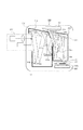
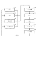
ここで、図3は、本発明の例示的な露光装置500の概略構成図である。
【0018】
本発明の露光装置500は、露光用の照明光としてEUV光(例えば、波長13.4nm)を用いて、例えば、ステップ・アンド・スキャン方式やステップ・アンド・リピート方式でマスク520に形成された回路パターンを被処理体540に露光する投影露光装置である。かかる露光装置は、サブミクロンやクオーターミクロン以下のリソグラフィー工程に好適であり、以下、本実施形態ではステップ・アンド・スキャン方式の露光装置(「スキャナー」とも呼ばれる。)を例に説明する。ここで、「ステップ・アンド・スキャン方式」とは、マスクに対してウェハを連続的にスキャン(走査)してマスクパターンをウェハに露光すると共に、1ショットの露光終了後ウェハをステップ移動して、次の露光領域に移動する露光方法である。「ステップ・アンド・リピート方式」は、上記の1ショットの露光を一括で行なうものである。
【0019】
図3を参照するに、露光装置500は、照明装置510と、マスク520と、マスク520を載置するマスクステージ525と、投影光学系530と、被処理体540と、被処理体540を載置するウェハステージ545と、アライメント検出機構550と、フォーカス位置検出機構560とを有する。
【0020】
また、図3に示すように、EUV光は、大気に対する透過率が低く、残留ガス(高分子有機ガスなど)成分との反応によりコンタミを生成してしまうため、少なくとも、EUV光が通る光路中(即ち、光学系全体)は真空雰囲気VC(もしくは減圧雰囲気でも構わない)となっている。
【0021】
照明装置510は、投影光学系530の円弧状の視野に対する円弧状のEUV光(例えば、波長13.4nm)によりマスク520を照明する照明装置であって、EUV光源512と、照明光学系514とを有する。
【0022】
EUV光源512は、例えば、レーザープラズマ光源が用いられる。これは、真空容器中のターゲット材に高強度のパルスレーザー光を照射し、高温のプラズマを発生させ、これから放射される、例えば、波長13nm程度のEUV光を利用するものである。ターゲット材としては、金属膜、ガスジェット、液滴などが用いられる。放射されるEUV光の平均強度を高くするためにはパルスレーザーの繰り返し周波数は高い方がよく、通常数kHzの繰り返し周波数で運転される。
【0023】
照明光学系514は、集光ミラー514a、オプティカルインテグレーター514bから構成される。集光ミラー514aは、レーザープラズマからほぼ等方的に放射されるEUV光集める役割を果たす。オプティカルインテグレーター514bは、マスク520を均一に所定の開口数で照明する役割を持っている。また、照明光学系514は、マスク520と共役な位置に、マスク520の照明領域を円弧状に限定するためのアパーチャ514cが設けられている。
【0024】
マスク520は、反射型マスクで、その上には転写されるべき回路パターン(又は像)が形成され、マスクステージに支持及び駆動されている。マスク520から発せられた回折光は、投影光学系530で反射されて被処理体540上に投影される。マスク520と被処理体540とは、光学的に共役の関係に配置される。露光装置500は、ステップ・アンド・スキャン方式の露光装置であるため、マスク520と被処理体540を走査することによりマスク520のパターンを被処理体540上に縮小投影する。
【0025】
マスクステージ525は、マスク520を支持して図示しない移動機構に接続されている。マスクステージ525は、当業界周知のいかなる構造をも適用することができる。図示しない移動機構は、リニアモーターなどで構成され、マスクステージ525を駆動することでマスク520を移動することができる。露光装置500は、マスク520と被処理体540を同期した状態で走査する。
【0026】
投影光学系530は、複数の反射ミラー(即ち、多層膜ミラー)530aを用いて、マスク520面上のパターンを像面である被処理体540上に縮小投影する。複数のミラー530aの枚数は、4枚乃至6枚程度である。少ない枚数のミラーで広い露光領域を実現するには、光軸から一定の距離だけ離れた細い円弧状の領域(リングフィールド)だけを用いて、マスク520と被処理体540を同時に走査して広い面積を転写する。投影光学系530の開口数(NA)は、0.2乃至0.3程度である。
【0027】
投影光学系、照明光学系の各ミラーはそれぞれミラーを一部囲む前述の鏡筒700によって支持されている。
【0028】
被処理体540は、本実施形態ではウェハであるが、液晶基板その他の被処理体を広く含む。被処理体540には、フォトレジストが塗布されている。
【0029】
ウェハステージ545は、ウェハチャック545aによって被処理体540を支持する。ウェハステージ545は、例えば、リニアモーターを利用して被処理体540を移動する。マスク520と被処理体540は、同期して走査される。また、マスクステージ525の位置とウェハステージ545との位置は、例えば、レーザー干渉計などにより監視され、両者は一定の速度比率で駆動される。
【0030】
アライメント検出機構550は、マスク520の位置と投影光学系530の光軸との位置関係、及び、被処理体540の位置と投影光学系530の光軸との位置関係を計測し、マスク520の投影像が被処理体540の所定の位置に一致するようにマスクステージ525及びウェハステージ545の位置と角度を設定する。
【0031】
フォーカス位置検出機構560は、被処理体540面でフォーカス位置を計測し、ウェハステージ545の位置及び角度を制御することによって、露光中、常時被処理体540面を投影光学系530による結像位置に保つ。
【0032】
露光において、照明装置510から射出されたEUV光はマスク520を照明し、マスク520面上のパターンを被処理体540面上に結像する。本実施形態において、像面は円弧状(リング状)の像面となり、マスク520と被処理体540を縮小倍率比の速度比で走査することにより、マスク520の全面を露光する。
【0033】
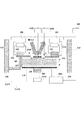
ここで、照明光学系514を構成するミラーである集光ミラー514aまたは、オプティカルインテグレーター514b、投影光学系530を構成するミラーであるミラー530aの近傍の概略図を図1に示す。
【0034】
真空チャンバVC内は、残留ガス成分と露光光Lとの反応によりミラーMの表面にコンタミが付着し、反射率が低下することを抑制するために、図示しない真空ポンプによって1×10⁻⁶[Pa]程度の真空に維持されている。
【0035】
真空チャンバVC内において、鏡筒700に支持されたミラーMは、支持部材MBを介して所定の場所にクランプ部材MCのよって位置決めされ、反射を利用して光を結像させる。ミラー近傍は、図1によく示されるように、ミラーを部分的に囲む鏡筒700、ミラーを鏡筒に支持する部材MB、ミラーをクランプする機構MC、ミラーを所定の温度範囲に制御冷却する冷却構成として、ミラー表面位置検出部400A,Bと、輻射機構200と、輻射機構制御部300、ミラー表面形状制御部600とを有する。本図では、特徴的に1つのミラーのみ部分的に囲むように図示した。勿論、鏡筒の内部に1つのミラーしか配置されている場合に限らず、鏡筒の内部に複数のミラーが配置されていても構わない。また、その複数のミラーそれぞれに輻射機構200等を配置しても良いし、複数のミラーのうち選択的に1つ以上のミラーに対して輻射機構200等を設けるようにしても構わない。
【0036】
ミラークランプ機構MCは、いわゆるエアシンリンダなどの圧空アクチュエータでミラーを3点でクランプするものである。
【0037】
ミラーを鏡筒に支持する部材MBは、特開平7−153663号公報のマスク保持方法に開示されているいわゆるキネマティックマウントと同様の構成を用いて、クランプ機構MCによって3点支持されたミラーの位置を6自由度すべてに対して過拘束なく拘束し、所定の位置へ支持している。
【0038】
輻射機構200は、ミラーに非接触で、露光光Lを遮らないように配置され、ミラーMに対して輻射によりミラーMから熱を吸収する。
【0039】
輻射機構200は、輻射板B、Rと、ペルチェ素子240と、放熱ブロック250と、循環部220Aとを有する。
【0040】
輻射板Bは、後述するペルチェ素子240が接合され、ペルチェ素子240のペルチェ効果により冷却されて、ミラーMに対して低温となり温度差を形成し、輻射によってミラーMの熱を吸収する。輻射板Rは、後述するペルチェ素子240が接合され、ペルチェ素子240のペルチェ効果により加熱されて、ミラーMに対して高温となり温度差を形成し、輻射によってミラーMに熱を与える。
【0041】
輻射板Bに接合されたペルチェ素子240は、ペルチェ素子に流す電流を変化させることによって、ペルチェ素子の吸熱面(ここでは、輻射板Bに接している面)と放熱面(ここでは放熱ブロック250と接している面)との温度差を変えることが可能である。さらに、放熱面を後述の放熱ブロックでほぼ一定の温度とすることで、吸熱面の温度を一定に保っている(温度上昇を防いでいる)。従って、ペルチェ素子240の吸熱面と接合された輻射板Bから、ミラーMの熱を吸収して冷却することができる。
【0042】
また、輻射板Rに接合されたペルチェ素子240も、ペルチェ素子に流す電流を変化させることによって、ペルチェ素子の吸熱面(ここでは、輻射板Rに接している面)と放熱面(ここでは放熱ブロック250と接している面)との温度差を変えることが可能である。さらに、吸熱面を後述の放熱ブロックでほぼ一定の温度とすることで、放熱面の温度を一定に保っている(温度低下を防いでいる)。
【0043】
従って、ペルチェ素子240の放熱面を輻射板Rと接合することで、輻射板Rから熱を放出して加熱することができる。ペルチェ素子240は、応答性が高いために高精度に輻射板B、Rの温度を制御して、ミラーMの温度を所定の値にすることができる。
【0044】
放熱ブロック250は、ペルチェ素子240の放熱面に接合されて、後述する循環部220Aが供給する熱媒体が流れるための流路を有する。流路は、パイプを介して循環部220Aと接続される。流路は、放熱ブロック250中に形成され、放熱ブロック250全面に一様に熱媒体が流れるように構成される。放熱ブロック250は、熱媒体により一定温度としている。
【0045】
循環部220Aは、パイプと接続されており、このパイプを介して熱媒体を放熱ブロック250の流路に供給及び循環させる。循環部220Aが流路に供給及び循環させる熱媒体は、放熱ブロック250の熱を回収し、放熱ブロックを略一定温度に保つためである。
【0046】
次に、ミラーの変形を抑制する機構について説明する。
【0047】
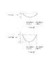
露光光が入射する前、つまりミラーMに熱歪を生じる前の段階で、計測系400Aによって照射領域のほぼ中心のZ方向位置Aを計測し、計測系400Bによって照射領域内の外周部分のZ方向位置Bを計測し、位置の差A−Bを求める。図2A参照。ここで、Z方向はミラーの面外方向、R方向とはミラーの面内方向を示す。
【0048】
露光光が入射すると前述のようにミラーMの温度分布が変化する。露光していない状態から、露光を開始する場合、ウエハを交換して、次のウエハを露光する場合などに大きく温度分布が変化する。
【0049】
温度分布は、照射領域の温度が他の部分に比べて上昇するように発生し、このために変形し、照射領域のほぼ中心のZ方向位置はA‘となり、照射領域内の外周部分のZ方向位置はB’となる(図2B参照)。この変形は主に単純な曲げの変形のため、ミラーの表裏面に温度差を積極的に与える事で、変形を低減する事ができる。
【0050】
この動作の詳細を以下に述べる。ミラー表面形状制御部600は、露光光が入射する前の熱変形の無い状態(図2Aの状態)での、照射領域のほぼ中心位置Aと、照射領域内の外周部分の位置Bの位置との差A−Bを求める。露光光が入射した後の照射領域のほぼ中心位置A‘と、照射領域内の外周部分の位置B’の位置との差A‘−B’が先に求めたA−Bとほぼ同じになるように、輻射機構制御部300を制御する。
【0051】
輻射機構制御部300は、輻射機構200を制御する。制御部300Aは、ペルチェ素子240に印加する印加電圧を変化させることで輻射板B、輻射板Rの温度を制御する。
【0052】
輻射によって、絶対温度T2[K]、面積A2[m2]の物質Yが絶対温度T1[K]、面積A1[m2]の物質Xから吸収する熱量は、物質Xの輻射率をE1、物質Yの輻射率をE2、輻射形態係数(即ち、物質Xから出たエネルギーが物質Yへ到達する割合)をF12とした場合に、熱流速密度Q[W/m2]を用いて以下の数式で表される。但し、T1>T2とする。
【0053】
(数1)
Q=5.67×10⁻⁸×(T1 4−T2 4)/((1−E1)/(E1×A1)+(1/(A2×F12))+(1−E2)/(E2×A2))
5.67×10⁻⁸:ステファン・ボルツマン定数
つまり、輻射形態係数が大きいほど、面積が大きいほど、輻射率が大きいほど輻射によって、より熱を与えたり、奪ったりする事ができる。
【0054】
輻射機構制御によって輻射板Bは低温に、輻射板Rは高温に制御されこれによって、前述の輻射によって、ミラーMの表面は冷やされ、裏面が温められることになり、露光熱によって変形するのと逆の曲げ変形を発生させ、露光熱による曲げ変形を低減する。
【0055】
この曲げ変形がほぼゼロつまり、A‘−B’=A−Bとなるように、輻射板Bと輻射板Rの温度を決める。
【0056】
以上のように動作させる事で、露光熱を吸収することで生じるミラー変形を低減する事ができるので、収差の悪化を低減でき、従来よりも微細な線幅を精度よく転写できる露光装置を提供できる。
【0057】
非接触にミラーの表面形状を変化させる事ができるため、発塵が無い。発生するパーティクル(微粒子)はたとえ50nm程度の大きさのものが1個であっても、ミラー表面、マスク、ウエハに付着すれば、回路欠陥となり、歩留まりが低下する。このような、問題を発生させる事が無い。
【0058】
また、本構成は、輻射板によってミラーの熱を吸収する効果も同時に持ち合わせているため、ミラーの温度はそれほど上昇する事が無いため、露光熱によるミラー表面形状の変化をもともと小さくできている。このように変形の小さいミラーの表面形状の変化を補正すればよいので、前述のような単純な構成で、ミラー変形をほぼゼロに低減する事ができる。
【0059】
輻射板の温度変動は、ペルチェ素子を用いれば一般的に0.01℃以下である。本発明の構成では、A‘−B’=−1nm、A−B=0nmの場合で、輻射板Bの温度をミラーの温度に対して−10℃、輻射板Rの温度をミラーの温度に対して+40℃にすれば、A‘−B’=A−B=0nmとする事ができる。つまり輻射板Rと輻射板Bの温度差50℃でミラーの表面形状を1nm補正する事ができる、先ほど述べたように0.01℃で輻射板の温度を制御すれば、理論的には、1nm/(50/0.01)といった、きわめて高精度に、表面形状を補正する事が可能となる。実際は、位置計測精度がそれほどないため、実際にはそこまで、高精度に補正する事はできないが、輻射板の温度安定性は、本発明では充分であることが分かる。
【0060】
以上はミラー表面の照射領域のほぼ中心位置のミラーのZ方向位置と、照射領域内の外周部分の位置のミラーのZ方向位置の2箇所をミラー表面形状の代表として計測した。露光の収差に影響するのは照射領域の変形であるため、照射領域のZ方向位置が所望の値になるようにするのが望ましいが、照射領域外の2箇所の位置のZ方向位置から照射領域のZ方向位置が推測できる場合には、照射領域外の2箇所の位置でのZ方向位置が所望の値となるように輻射板B、Rの温度を制御しても良い。
【0061】
また、本実施形態は上記の形態に限られたものではない。露光装置によるミラーへの露光光の照射領域は、必ずしも回転対称ではなく、走査型露光装置等では略長方形であったり、またその他非回転対称な形状をしていることがある。
【0062】
このように照射領域が非回転対称な形状をしていると、ミラーMの平面内の互いに異なる方向に関しては、露光光がミラーMに与える熱量の分布が異なる。露光光がミラーMに与える熱量の分布が異なると、当然ミラーMの変形の仕方、変形量も異なってしまう。
【0063】
そこで、ミラー位置検出部400Aを、照射領域の略中心に配置し、さらに照射領域内の外周部に複数のミラー位置検出部(400Bも含む)を配置し、ミラー平面内の各方向に関するミラーの変形を計測し、その計測結果に基づいてミラーの温度制御を行うようにする。例えば、輻射板Bを、照射領域内の外周部に配置したミラー位置検出部に対応する領域ごとに分割し、それぞれの位置検出結果に基づいて、分割した輻射板Bそれぞれの温度を制御するようにすれば良い。勿論、照射領域内の外周部に配置したミラー位置検出部の数と、輻射板Bの分割数を必ずしも一致させる必要は無いし、輻射板Bを分割するのと同様に輻射板Rも分割してそれぞれを温度制御するようにしても良い。
【0064】
走査型露光装置においては、ミラーに対する光の照射領域が略長方形形のスリット状となることが多い。その場合、このスリットの長手方向と短手方向との間で、ミラーが受ける熱量の分布の差が顕著に現れる。そこで、照射領域内の中心と、照射領域の中心からスリットの長手方向にシフトした位置(好ましくは照射領域内の外周部)と、照射領域の中心からスリットの短手方向にシフトした位置(好ましくは照射領域内の外周部)との少なくとも3箇所(それぞれのシフトした方向の両端であれば5箇所)に、ミラーの位置検出部を設けるのが好ましい。そして、その際、輻射板B(輻射板Rも含めても良い)を、スリットの長手方向の両端と、スリットの短手方向の両端との少なくとも4つ以上に分割し、それぞれ独立に温度制御が可能な構成にすると、スリットの長手方向と短手方向とで熱量分布、温度分布、変形量等が異なった場合でも、対応可能となる。
【0065】
ここで、前述したいように、ミラー位置検出部は、必ずしもミラーに光が照射される領域内のミラー位置を検出する必要は無く、照射領域外のミラー位置を検出しても構わないが、少なくともミラーの2箇所以上の位置を検出するように構成するのが望ましい。
【0066】
また、上述のように、ミラーの温度を制御するのに加えて、ミラーの材料を工夫しても構わない。例えば、Zerodur(商品名)やULE(商品名)のようなガラスセラミクス材料は、線膨張係数が低い。そこで、本実施例では、線膨張係数が0ppb以上15ppb以下、より好ましくは5ppb以上10ppb以下であるような材料を用いてミラーを構成するのが好ましい。勿論、Zerodur(商品名)やULEで構成するのはミラーの基板部分であり、その基板の上にMo膜とSi膜とで多層膜を形成し、反射面を形成する。
【0067】
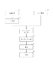
次に、図4及び図5を参照して、上述の露光装置500を利用したデバイス製造方法の実施例を説明する。図4は、デバイス(ICやLSIなどの半導体チップ、LCD、CCD等)の製造を説明するためのフローチャートである。本実施形態においては、半導体チップの製造を例に説明する。ステップ1(回路設計)では、デバイスの回路設計を行う。ステップ2(マスク製作)では、設計した回路パターンを形成したマスクを製作する。ステップ3(ウェハ製造)では、シリコンなどの材料を用いてウェハを製造する。ステップ4(ウェハプロセス)は、前工程と呼ばれ、マスクとウェハを用いてリソグラフィー技術によってウェハ上に実際の回路を形成する。ステップ5(組み立て)は、後工程と呼ばれ、ステップ4によって作成されたウェハを用いて半導体チップ化する工程であり、アッセンブリ工程(ダイシング、ボンディング)、パッケージング工程(チップ封入)等の工程を含む。ステップ6(検査)では、ステップ5で作成された半導体デバイスの動作確認テスト、耐久性テストなどの検査を行う。こうした工程を経て半導体デバイスが完成し、それが出荷(ステップ7)される。
【0068】
図5は、ステップ4のウェハプロセスの詳細なフローチャートである。ステップ11(酸化)では、ウェハの表面を酸化させる。ステップ12(CVD)では、ウェハの表面に絶縁膜を形成する。ステップ14(イオン打ち込み)では、ウェハにイオンを打ち込む。ステップ15(レジスト処理)では、ウェハに感光剤を塗布する。ステップ16(露光)では、露光装置500によってマスクの回路パターンをウェハに露光する。ステップ17(現像)では、露光したウェハを現像する。ステップ18(エッチング)では、現像したレジスト像以外の部分を削り取る。ステップ19(レジスト剥離)では、エッチングが済んで不要となったレジストを取り除く。これらのステップを繰り返し行うことによってウェハ上に多重に回路パターンが形成される。本実施形態のデバイス製造方法によれば、従来よりも高品位のデバイスを製造することができる。このように、露光装置500を使用するデバイス製造方法、並びに結果物としてのデバイスも本発明の一側面を構成する。
【0069】
また、本発明はこれらの実施例に限定されないことはいうまでもなく、その要旨の範囲内で種々の変形及び変更が可能である。
【0070】
また、本発明の実施態様を以下のように記載することもできる。
【0071】
(実施態様1)
内部空間に少なくとも1つの光学素子を有し、光源からの光を所定面に導く光学系であって、
前記少なくとも1つの光学素子の表面形状を測定する測定系と、
前記測定系の測定結果に基づいて、前記少なくとも1つの光学素子の温度制御を行う温度制御部とを有することを特徴とする光学系。
【0072】
(実施態様2)
前記温度制御部は、前記少なくとも1つの光学素子の表面側に配置された第1温度制御部と、前記少なくとも1つの光学素子の裏面側に配置された第2温度制御部とを有していることを特徴とする実施態様1記載の光学系。
【0073】
(実施態様3)
前記温度制御部は、前記少なくとも1つの光学素子に曲げ応力を発生させることを特徴とする実施態様1又は2記載の光学系。
【0074】
(実施態様4)
前記測定系は、前記光学素子面内の互いに略垂直な2方向に関する、前記光学素子の変形を計測することが可能であることを特徴とする実施態様1乃至3いずれかに記載の光学系。
【0075】
(実施態様5)
前記略垂直な2方向が、前記少なくとも1つの光学素子に光が照射される領域の長手方向と短手方向と略一致している(誤差は略10度以内)ことを特徴とする実施態様4記載の光学系。
【0076】
(実施態様6)
前記測定系により計測した、前記略垂直な2方向に関する前記光学素子の変形を抑制するように、前記温度制御部が温度制御を行うことを特徴とする実施態様4又は5記載の光学系。
【0077】
(実施態様7)
前記温度制御部は、前記光学素子の異なる領域に対して異なる温度制御を行うことが可能であることを特徴とする実施態様1乃至6いずれかに記載の光学系。
【0078】
(実施態様8)
前記測定系は、前記少なくとも1つの光学素子の表面の2箇所以上の測定位置を測定することを特徴とする実施態様1乃至6いずれかに記載の光学系。
【0079】
(実施態様9)
前記2箇所以上の測定位置のうちの少なくとも1箇所の測定位置は、前記少なくとも1つの光学素子の前記光が照射される領域内であることを特徴とする実施態様8記載の光学系。
【0080】
(実施態様10)
前記2箇所以上の測定位置のうちの少なくとも1箇所の測定位置は、前記少なくとも1つの光学素子の前記光が照射される領域外であることを特徴とする実施態様8記載の光学系。
【0081】
(実施態様11)
前記2箇所以上の測定位置は、前記少なくとも1つの光学素子の前記光が照射される領域内であることを特徴とする実施態様8記載の光学系。
【0082】
(実施態様12)
前記2箇所以上の測定位置は、前記少なくとも1つの光学素子の前記光が照射される領域外であることを特徴とする実施態様8記載の光学系。
【0083】
(実施態様13)
前記2箇所以上の測定位置のうちの1箇所の測定位置が、前記少なくとも1つの光学素子の前記光が照射される領域の略中心であることを特徴とする実施態様8記載の光学系。
【0084】
(実施態様14)
前記2箇所以上の測定位置のうちの1箇所の測定位置が、前記少なくとも1つの光学素子の前記光が照射される領域の略外周部分であることを特徴とする実施態様8記載の光学系。
【0085】
(実施態様15)
前記測定系は、前記少なくとも1つの光学素子の表面の3箇所以上の測定位置を測定することを特徴とする実施態様1乃至14いずれかに記載の光学系。
【0086】
(実施態様16)
前記少なくとも1つの光学素子は反射部材であることを特徴とする実施態様1乃至15いずれかに記載の光学系。
【0087】
(実施態様17)
前記測定系は、前記反射部材の反射面の形状を測定することを特徴とする実施態様16記載の光学系。
【0088】
(実施態様18)
前記温度制御部は、前記反射部材の反射面側と前記反射部材の裏面側とにそれぞれ配置されていることを特徴とする実施態様16又は17記載の光学系。
【0089】
(実施態様19)
前記反射面側に配置された温度制御部は、独立に温度制御が可能な複数の領域を有しており、前記測定系の測定結果に従って、複数の領域のそれぞれを独立に温度制御することを特徴とする実施態様18記載の光学系。
【0090】
(実施態様20)
前記温度制御部は、前記反射部材の反射面を冷却し、前記反射部材の反射面の裏側の面を加熱することを特徴とする実施態様16乃至19いずれに記載の光学系。
【0091】
(実施態様21)
前記少なくとも1つの光学素子の線膨張係数が、0ppb以上15ppb以下であることを特徴とする実施態様1乃至20いずれかに記載の実施態様1乃至20いずれかに記載の光学系。
【0092】
(実施態様22)
前記少なくとも1つの光学素子の線膨張係数が、5ppb以上10ppb以下であることを特徴とする実施態様1乃至21いずれかに記載の実施態様1乃至22いずれかに記載の光学系。
【0093】
(実施態様23)
前記内部空間は、高真空であることを特徴とする実施態様1乃至22いずれかに記載の光学系。
【0094】
(実施態様24)
前記光源からの光がEUV光(波長13〜14nm)であることを特徴とする実施態様1乃至23いずれかに記載の光学系。
【0095】
(実施態様25)
前記温度制御部は、前記少なくとも1つの光学素子を、輻射により温度制御することを特徴とする実施態様1乃至24いずれかに記載の光学系。
【0096】
(実施態様26)
前記温度制御部は、前記少なくとも1つの光学素子を温度制御するための輻射板を有し、該輻射板をペルチェ素子により温度制御していることを特徴とする実施態様1乃至25いずれかに記載の光学系。
【0097】
(実施態様27)
前記輻射板と前記ペルチェ素子とが接触して配置されており、前記ペルチェ素子の前記輻射板と反対側の面には、略一定温度に保たれた放熱部が配置されていることを特徴とする実施態様26記載の光学系。
【0098】
(実施態様28)
実施態様1乃至27いずれかに記載の光学系を有する露光装置。
【0099】
(実施態様29)
前記光源からの光で前記所定面に配置された被露光体を露光する露光装置であって、前記光源から前記被露光体までの光路に配置された光学素子がすべて反射部材であることを特徴とする実施態様28記載の露光装置。
【0100】
(実施態様30)
EUVを露光光とする露光装置であって、
複数のミラーからなり、光源から放射されたEUV光を反射型マスクへ導く照明光学系と、
複数のミラーからなり、前記マスクからの反射光を被露光体上に結像させる投影光学系と、
前記複数のミラーのうち少なくとも1つのミラーの表面の温度を非接触に変化させる機構と、
前記複数のミラーのうち少なくとも1つのミラーの裏面の温度を非接触に変化させる機構と、
前記ミラーの表面形状を測定する測定系と、
前記測定系による測定結果に基づき前記ミラー表面または裏面の温度を非接触に変化させる機構を制御する制御器を有することを特徴とする露光装置。
【0101】
(実施態様31)
実施態様28乃至30いずれかに記載の露光装置を用いて被露光体を露光するステップと、露光された前記被露光体を現像するステップとを有することを特徴とするデバイス製造方法。
【0102】
このような構成にすることにより、露光光を光学素子が吸収することで変形する事を低減し、光学特性の収差を改善できる光学系、露光装置を提供できる。さらに、光学特性に影響を与えるミラーの露光光照射領域の形状を直接計測して、この変形を低減するので、より高精度に光学特性の収差を改善できる露光装置を提供できる。さらに、露光光を光学素子が吸収することで変形する事を低減し、光学特性の収差を改善できる露光方法を提供できる。
【0103】
さらに、上述の露光装置の作用と同様の作用を奏するデバイス製造方法は、中間及び最終結果物であるデバイス自体にもその効力が及ぶ。また、かかるデバイスは、LSIやVLSIなどの半導体チップ、CCD、LCD、磁気センサー、薄膜磁気ヘッドなどを含む。
【0104】
【発明の効果】
本願に記載した発明によれば、
従来よりも微細な線幅を精度よく転写できる露光装置、露光方法を提供できる。
【0105】
さらに、本願の請求項21に記載した発明によれば、従来よりも高品位のデバイスを製造することができる。
【図面の簡単な説明】
【図1】本発明の一側面としての露光装置を示す概略構成図である。
【図2】露光光が照射されたことによって発生するミラー表面の形状変化を説明する概略図。
【図3】本発明の例示的な露光装置の概略構成図である。
【図4】デバイス(ICやLSIなどの半導体チップ、LCD、CCD等)の製造を説明するためのフローチャートである。
【図5】図4に示すステップ4のウェハプロセスの詳細なフローチャートである。
【符号の説明】
200B 輻射機構(冷却)
200R 輻射機構(加熱)
B 輻射板(冷却)
R 輻射板(加熱)
220A 循環部
300A 制御部
240 ペルチェ素子
250 放熱ブロック
500 露光装置
512 照明光学系
512a 集光ミラー
512a オプティカルインテグレーター
530 投影光学系
530a 反射ミラー
400A ミラー表面位置検出部400(照射領域内の中心)
400B ミラー表面位置検出部400(照射領域内の外周)
600 ミラー表面形状制御部
700 鏡筒[0001]
BACKGROUND OF THE INVENTION
The present invention generally relates to a mirror holding device, and more particularly, to an exposure device that exposes an object to be processed such as a single crystal substrate for a semiconductor wafer and a glass substrate for a liquid crystal display (LCD). The present invention is particularly suitable for an exposure apparatus that uses ultraviolet or extreme ultraviolet (EUV) light as an exposure light source.
[0002]
[Prior art]
When a fine semiconductor element such as a semiconductor memory or a logic circuit is manufactured using a photolithography technique, a circuit pattern drawn on a reticle or a mask (these terms are used interchangeably in this application). Conventionally, a reduction projection exposure apparatus that projects a circuit pattern by projecting the image onto a wafer or the like by a projection optical system has been used.
[0003]
The minimum dimension (resolution) that can be transferred by the reduction projection exposure apparatus is proportional to the wavelength of light used for exposure and inversely proportional to the numerical aperture (NA) of the projection optical system. Therefore, the shorter the wavelength, the better the resolution. For this reason, with the recent demand for miniaturization of semiconductor elements, the exposure light has been shortened, and an ultra-high pressure mercury lamp (i-line (wavelength: about 365 nm)), KrF excimer laser (wavelength: about 248 nm), ArF excimer. The wavelength of ultraviolet light used with lasers (wavelength about 193 nm) has become shorter.
[0004]
However, semiconductor elements are rapidly miniaturized, and there is a limit in lithography using ultraviolet light. Therefore, in order to efficiently transfer a very fine circuit pattern of 0.1 μm or less, a reduction projection exposure apparatus using extreme ultraviolet (EUV) light having a wavelength shorter than that of ultraviolet light and having a wavelength of about 10 nm to 15 nm ( Hereinafter, it is referred to as “EUV exposure apparatus”).
[0005]
As exposure light becomes shorter in wavelength, the absorption of light by the substance becomes very large. Therefore, it is difficult to use a refraction element utilizing light refraction such as that used in visible light or ultraviolet light, that is, a lens. In the wavelength region of EUV light, there is no glass material that can be used, and a reflective element that uses light reflection, that is, a reflective optical system that constitutes an optical system only with a mirror (for example, a multilayer mirror) is used.
[0006]
The mirror does not reflect all the exposure light, but absorbs 30% or more of the exposure light. The absorbed exposure light becomes heat and deforms the surface shape of the mirror, causing deterioration of optical performance (particularly imaging performance). Therefore, the mirror is made of a low thermal expansion glass having a small linear expansion coefficient, for example, a linear expansion coefficient of 10 ppb, in order to reduce a change in the mirror shape due to a temperature change.
[0007]
Since the EUV exposure apparatus is used for exposure of a circuit pattern of 0.1 μm or less, the line width accuracy is very strict, and the mirror surface shape can only be deformed to about 0.1 nm or less. Therefore, even if the linear expansion coefficient of the mirror is set to 20 ppb, the temperature gradually increases due to absorption of exposure light, and the shape of the mirror surface changes. For example, if the thickness of the mirror is 50 mm, the shape of the mirror surface changes by 0.1 nm due to a temperature rise of 0.1 ° C.
[0008]
Therefore, for example, Japanese Patent Application Laid-Open No. 05-29117 discloses a projection exposure apparatus in which the shape of the mirror is kept constant by keeping the amount of heat applied to the mirror constant.
[0009]
Further, as a means for correcting the surface shape of the deformed mirror, as disclosed in Japanese Patent Application Laid-Open No. 2000-286191, a proposal for correcting the mirror back surface with a plurality of pins has been made.
[0010]
[Patent Document 1]
Japanese Patent Laid-Open No. 05-029117
[Patent Document 2]
JP 2000-286191 A
[0011]
[Problems to be solved by the invention]
However, in the exposure apparatus disclosed in Japanese Patent Application Laid-Open No. 05-29117, the amount of heat applied to the mirror is not always constant during exposure, and varies depending on the pattern, so it is difficult to always keep the amount of heat applied to the mirror constant. Furthermore, even if the amount of heat applied to the mirror is kept constant, if the location and distribution of the amount of heat is different, the mirror's deformation method will change, so the amount of heat is kept constant. There is a problem that is not necessarily constant.
[0012]
In addition, in the exposure apparatus disclosed in Japanese Patent Laid-Open No. 2000-286191, if the position stability of the correction driving pin is poor by 0.1 nm or more, the mirror surface is deformed so that the aberration is worsened. .
[0013]
Accordingly, an object of the present invention is to provide an exposure apparatus that reduces deformation due to thermal expansion of a mirror that causes deterioration in imaging performance and provides desired optical performance.
[0014]
[Means for Solving the Problems]
In order to solve the above problems, the optical system of the present invention has at least one internal space.Reflective memberAn optical system for guiding light from a light source, wherein the at least oneReflective memberofReflective surfaceA measuring system for measuring the shape;A first temperature control unit disposed on a reflective surface side of the at least one reflective member and cooling the at least one reflective member; and disposed on a back surface side of the at least one reflective member, wherein the at least one reflective member is A second temperature control unit for heating, and the first and second temperature control units perform temperature control of the at least one reflecting member based on a measurement result of the measurement system.It is characterized by that.
[0015]
Further objects and other features of the present invention will become apparent from the preferred embodiments described below with reference to the accompanying drawings.
[0016]
DETAILED DESCRIPTION OF THE INVENTION
Hereinafter, an exposure apparatus which is an exemplary embodiment of the present invention will be described with reference to the accompanying drawings. In addition, in each figure, about the same member, the same reference number is attached | subjected and the overlapping description is abbreviate | omitted.
[0017]
Here, FIG. 3 is a schematic block diagram of an
[0018]
The
[0019]
Referring to FIG. 3, an
[0020]
Further, as shown in FIG. 3, EUV light has a low transmittance to the atmosphere and generates contamination due to a reaction with a residual gas (polymer organic gas or the like) component, so at least in the optical path through which the EUV light passes. That is, the entire optical system is in a vacuum atmosphere VC (or a reduced pressure atmosphere).
[0021]
The
[0022]
As the EUV
[0023]
The illumination
[0024]
The mask 520 is a reflective mask, on which a circuit pattern (or image) to be transferred is formed, and is supported and driven by a mask stage. The diffracted light emitted from the mask 520 is reflected by the projection
[0025]
The mask stage 525 supports the mask 520 and is connected to a moving mechanism (not shown). The mask stage 525 may employ any structure known in the art. A moving mechanism (not shown) is configured by a linear motor or the like, and can move the mask 520 by driving the mask stage 525. The
[0026]
The projection
[0027]
Each mirror of the projection optical system and the illumination optical system is supported by the
[0028]
The object to be processed 540 is a wafer in the present embodiment, but widely includes liquid crystal substrates and other objects to be processed. A photoresist is applied to the object to be processed 540.
[0029]
[0030]
The
[0031]
The focus
[0032]
In the exposure, the EUV light emitted from the
[0033]
Here, FIG. 1 shows a schematic diagram of the vicinity of a
[0034]
In the vacuum chamber VC, in order to prevent the contamination from adhering to the surface of the mirror M due to the reaction between the residual gas component and the exposure light L and reducing the reflectance, a vacuum pump (not shown) is used.-6A vacuum of about [Pa] is maintained.
[0035]
In the vacuum chamber VC, the mirror M supported by the
[0036]
The mirror clamp mechanism MC clamps the mirror at three points with a pneumatic actuator such as a so-called air cylinder.
[0037]
The member MB for supporting the mirror on the lens barrel is the same as that of the so-called kinematic mount disclosed in the mask holding method disclosed in JP-A-7-153663, and the mirror MB supported at three points by the clamp mechanism MC. The position is constrained without over-constraint for all six degrees of freedom and is supported at a predetermined position.
[0038]
The
[0039]
The
[0040]
The radiation plate B is joined with a
[0041]
The
[0042]
Further, the
[0043]
Therefore, by joining the heat dissipation surface of the
[0044]
The
[0045]
The
[0046]
Next, a mechanism for suppressing the deformation of the mirror will be described.
[0047]
Before the exposure light is incident, that is, before the thermal distortion occurs in the mirror M, the
[0048]
When exposure light is incident, the temperature distribution of the mirror M changes as described above. When exposure is started from an unexposed state, the temperature distribution greatly changes when the wafer is replaced and the next wafer is exposed.
[0049]
The temperature distribution is generated such that the temperature of the irradiation region rises as compared with other portions, and is deformed for this reason, and the position in the Z direction at the substantially center of the irradiation region becomes A ′, and the Z of the outer peripheral portion in the irradiation region The direction position is B ′ (see FIG. 2B). Since this deformation is mainly a simple bending deformation, the deformation can be reduced by positively applying a temperature difference between the front and back surfaces of the mirror.
[0050]
Details of this operation will be described below. The mirror surface
[0051]
The radiation
[0052]
Absolute temperature T due to radiation2[K], area A2[M2The substance Y of the absolute temperature T1[K], area A1[M2The amount of heat absorbed from the substance X in Eq.1, The emissivity of substance Y is E2, The radiation form factor (that is, the rate at which the energy from the substance X reaches the substance Y) F12The heat flow density Q [W / m2] Is expressed by the following mathematical formula. However, T1> T2And
[0053]
(Equation 1)
Q = 5.67 × 10⁻⁸× (T1 4-T2 4) / ((1-E1) / (E1× A1) + (1 / (A2× F12)) + (1-E2) / (E2× A2))
5.67 × 10⁻⁸: Stefan-Boltzmann constant
That is, the larger the radiation form factor, the larger the area, and the greater the radiation rate, the more heat can be applied or removed by radiation.
[0054]
By controlling the radiation mechanism, the radiation plate B is controlled to a low temperature and the radiation plate R is controlled to a high temperature. As a result, the surface of the mirror M is cooled and the back surface is heated by the radiation described above, and is deformed by the exposure heat. Reverse bending deformation is generated, and bending deformation due to exposure heat is reduced.
[0055]
The temperatures of the radiation plate B and the radiation plate R are determined so that the bending deformation is almost zero, that is, A′−B ′ = A−B.
[0056]
By operating as described above, mirror deformation caused by absorbing exposure heat can be reduced, so that an exposure apparatus that can reduce aberration deterioration and transfer a finer line width more accurately than before can be provided. it can.
[0057]
Since the surface shape of the mirror can be changed in a non-contact manner, there is no dust generation. Even if the generated particles (fine particles) are only one having a size of about 50 nm, if they adhere to the mirror surface, mask, or wafer, they will cause circuit defects and yield will be reduced. There is no such a problem.
[0058]
In addition, since this configuration also has the effect of absorbing the heat of the mirror by the radiation plate, the temperature of the mirror does not rise so much, so that the change in the mirror surface shape due to the heat of exposure can be reduced originally. Since it is sufficient to correct the change in the surface shape of the mirror with a small deformation in this way, the mirror deformation can be reduced to almost zero with the simple configuration as described above.
[0059]
The temperature fluctuation of the radiation plate is generally 0.01 ° C. or less when a Peltier element is used. In the configuration of the present invention, in the case of A′−B ′ = − 1 nm and AB = 0 nm, the temperature of the radiation plate B is −10 ° C. with respect to the mirror temperature, and the temperature of the radiation plate R is the mirror temperature. On the other hand, if the temperature is + 40 ° C., A′−B ′ = A−B = 0 nm. That is, the surface shape of the mirror can be corrected by 1 nm when the temperature difference between the radiation plate R and the radiation plate B is 50 ° C. If the temperature of the radiation plate is controlled at 0.01 ° C. as described above, theoretically, The surface shape can be corrected with extremely high accuracy of 1 nm / (50 / 0.01). Actually, since the position measurement accuracy is not so much, it cannot be corrected so accurately in practice, but it is understood that the temperature stability of the radiation plate is sufficient in the present invention.
[0060]
As described above, two mirror positions are measured as representatives of the mirror surface shape: the Z-direction position of the mirror substantially at the center of the irradiation area on the mirror surface, and the Z-direction position of the mirror at the position of the outer peripheral portion in the irradiation area. Since it is the deformation of the irradiation region that affects the aberration of exposure, it is desirable to set the Z direction position of the irradiation region to a desired value. However, irradiation is performed from two Z position positions outside the irradiation region. When the Z direction position of the region can be estimated, the temperatures of the radiation plates B and R may be controlled so that the Z direction positions at two positions outside the irradiation region have desired values.
[0061]
Further, the present embodiment is not limited to the above form. The irradiation area of the exposure light onto the mirror by the exposure apparatus is not necessarily rotationally symmetric, and may be substantially rectangular or other non-rotationally symmetric in a scanning exposure apparatus or the like.
[0062]
When the irradiation region has a non-rotationally symmetric shape in this way, the distribution of the amount of heat given to the mirror M by the exposure light differs in different directions in the plane of the mirror M. If the distribution of the amount of heat given to the mirror M by the exposure light is different, the manner of deformation and the amount of deformation of the mirror M will naturally be different.
[0063]
Therefore, the mirror
[0064]
In a scanning exposure apparatus, a light irradiation area on a mirror often has a substantially rectangular slit shape. In that case, a difference in the distribution of the amount of heat received by the mirror appears significantly between the longitudinal direction and the short direction of the slit. Therefore, the center in the irradiation area, the position shifted from the center of the irradiation area in the longitudinal direction of the slit (preferably the outer peripheral part in the irradiation area), and the position shifted from the center of the irradiation area in the short direction of the slit (preferably Are preferably provided with mirror position detection portions at at least three locations (the outer peripheral portion in the irradiation region) (5 locations if both ends in each shifted direction). At that time, the radiating plate B (which may include the radiating plate R) is divided into at least four of both ends in the longitudinal direction of the slit and both ends in the short direction of the slit, and the temperature is controlled independently. If the configuration is capable of handling, even when the heat amount distribution, the temperature distribution, the deformation amount, and the like are different between the longitudinal direction and the short direction of the slit, it is possible to cope.
[0065]
Here, as described above, the mirror position detection unit does not necessarily detect the mirror position in the region where the mirror is irradiated with light, and may detect the mirror position outside the irradiation region, but at least It is desirable to configure to detect two or more positions of the mirror.
[0066]
Further, as described above, in addition to controlling the mirror temperature, the mirror material may be devised. For example, glass ceramic materials such as Zerodur (trade name) and ULE (trade name) have a low coefficient of linear expansion. Therefore, in this embodiment, it is preferable to configure the mirror using a material whose linear expansion coefficient is 0 ppb or more and 15 ppb or less, more preferably 5 ppb or more and 10 ppb or less. Of course, it is the substrate portion of the mirror that is composed of Zerodur (trade name) or ULE, and a multilayer film is formed on the substrate by a Mo film and an Si film to form a reflective surface.
[0067]
Next, an embodiment of a device manufacturing method using the above-described
[0068]
FIG. 5 is a detailed flowchart of the wafer process in Step 4. In step 11 (oxidation), the surface of the wafer is oxidized. In step 12 (CVD), an insulating film is formed on the surface of the wafer. Step 14 (ion implantation) implants ions into the wafer. In step 15 (resist process), a photosensitive agent is applied to the wafer. Step 16 (exposure) uses the
[0069]
Needless to say, the present invention is not limited to these examples, and various modifications and changes can be made within the scope of the invention.
[0070]
The embodiment of the present invention can also be described as follows.
[0071]
(Embodiment 1)
An optical system having at least one optical element in an internal space and guiding light from a light source to a predetermined surface,
A measurement system for measuring a surface shape of the at least one optical element;
An optical system comprising: a temperature control unit that performs temperature control of the at least one optical element based on a measurement result of the measurement system.
[0072]
(Embodiment 2)
The temperature control unit includes a first temperature control unit disposed on the front surface side of the at least one optical element, and a second temperature control unit disposed on the back surface side of the at least one optical element. The optical system according to Embodiment 1, wherein
[0073]
(Embodiment 3)
The optical system according to
[0074]
(Embodiment 4)
The optical system according to any one of embodiments 1 to 3, wherein the measurement system is capable of measuring deformation of the optical element in two directions that are substantially perpendicular to each other in the plane of the optical element.
[0075]
(Embodiment 5)
Embodiment 4 wherein the two substantially perpendicular directions substantially coincide with a longitudinal direction and a lateral direction of an area where light is irradiated to the at least one optical element (an error is within approximately 10 degrees). The optical system described.
[0076]
(Embodiment 6)
6. The optical system according to embodiment 4 or 5, wherein the temperature control unit performs temperature control so as to suppress deformation of the optical element in the substantially perpendicular two directions measured by the measurement system.
[0077]
(Embodiment 7)
The optical system according to any one of embodiments 1 to 6, wherein the temperature control unit is capable of performing different temperature control on different regions of the optical element.
[0078]
(Embodiment 8)
The optical system according to any one of embodiments 1 to 6, wherein the measurement system measures two or more measurement positions on the surface of the at least one optical element.
[0079]
(Embodiment 9)
9. The optical system according to claim 8, wherein at least one measurement position among the two or more measurement positions is within a region irradiated with the light of the at least one optical element.
[0080]
(Embodiment 10)
9. The optical system according to claim 8, wherein at least one of the two or more measurement positions is outside a region irradiated with the light of the at least one optical element.
[0081]
(Embodiment 11)
9. The optical system according to claim 8, wherein the two or more measurement positions are in a region irradiated with the light of the at least one optical element.
[0082]
(Embodiment 12)
9. The optical system according to claim 8, wherein the two or more measurement positions are outside a region irradiated with the light of the at least one optical element.
[0083]
(Embodiment 13)
9. The optical system according to claim 8, wherein one of the two or more measurement positions is substantially the center of a region irradiated with the light of the at least one optical element.
[0084]
(Embodiment 14)
9. The optical system according to embodiment 8, wherein one of the two or more measurement positions is a substantially outer peripheral portion of the region irradiated with the light of the at least one optical element.
[0085]
(Embodiment 15)
15. The optical system according to any one of embodiments 1 to 14, wherein the measurement system measures three or more measurement positions on the surface of the at least one optical element.
[0086]
(Embodiment 16)
16. The optical system according to any one of embodiments 1 to 15, wherein the at least one optical element is a reflecting member.
[0087]
(Embodiment 17)
17. The optical system according to claim 16, wherein the measurement system measures the shape of the reflection surface of the reflection member.
[0088]
(Embodiment 18)
18. The optical system according to embodiment 16 or 17, wherein the temperature control unit is arranged on each of a reflection surface side of the reflection member and a back surface side of the reflection member.
[0089]
(Embodiment 19)
The temperature control unit disposed on the reflective surface side has a plurality of regions that can be controlled independently, and controls each of the plurality of regions independently according to the measurement result of the measurement system. An optical system according to
[0090]
(Embodiment 20)
20. The optical system according to any one of embodiments 16 to 19, wherein the temperature control unit cools the reflecting surface of the reflecting member and heats the surface on the back side of the reflecting surface of the reflecting member.
[0091]
(Embodiment 21)
21. The optical system according to any one of Embodiments 1 to 20, wherein a linear expansion coefficient of the at least one optical element is 0 ppb or more and 15 ppb or less.
[0092]
(Embodiment 22)
23. The optical system according to any one of Embodiments 1 to 22, wherein the linear expansion coefficient of the at least one optical element is 5 ppb or more and 10 ppb or less.
[0093]
(Embodiment 23)
23. The optical system according to any one of embodiments 1 to 22, wherein the internal space is a high vacuum.
[0094]
(Embodiment 24)
24. The optical system according to any one of embodiments 1 to 23, wherein the light from the light source is EUV light (
[0095]
(Embodiment 25)
25. The optical system according to any one of embodiments 1 to 24, wherein the temperature control unit controls the temperature of the at least one optical element by radiation.
[0096]
(Embodiment 26)
The temperature control unit has a radiation plate for controlling the temperature of the at least one optical element, and the temperature of the radiation plate is controlled by a Peltier element. Optical system.
[0097]
(Embodiment 27)
The radiation plate and the Peltier element are arranged in contact with each other, and a heat radiating portion kept at a substantially constant temperature is arranged on the surface of the Peltier element opposite to the radiation plate. An optical system according to Embodiment 26.
[0098]
(Embodiment 28)
An exposure apparatus comprising the optical system according to any one of embodiments 1 to 27.
[0099]
(Embodiment 29)
An exposure apparatus that exposes an object to be exposed disposed on the predetermined surface with light from the light source, wherein all of the optical elements disposed in an optical path from the light source to the object to be exposed are reflecting members. The exposure apparatus according to embodiment 28.
[0100]
(Embodiment 30)
An exposure apparatus using EUV as exposure light,
An illumination optical system that includes a plurality of mirrors and guides EUV light emitted from a light source to a reflective mask;
A projection optical system comprising a plurality of mirrors, and forming an image of reflected light from the mask on an object to be exposed;
A mechanism for changing the temperature of the surface of at least one of the plurality of mirrors in a non-contact manner;
A mechanism for changing the temperature of the back surface of at least one of the plurality of mirrors to a non-contact state;
A measurement system for measuring the surface shape of the mirror;
An exposure apparatus comprising: a controller that controls a mechanism for changing the temperature of the mirror front or back surface in a non-contact manner based on a measurement result by the measurement system.
[0101]
(Embodiment 31)
31. A device manufacturing method comprising: exposing an object to be exposed using the exposure apparatus according to any one of Embodiments 28 to 30; and developing the exposed object to be exposed.
[0102]
By adopting such a configuration, it is possible to provide an optical system and an exposure apparatus that can reduce deformation due to absorption of exposure light by an optical element and improve aberration of optical characteristics. Furthermore, since the deformation of the exposure light irradiation area of the mirror that affects the optical characteristics is directly measured and this deformation is reduced, an exposure apparatus that can improve aberrations of the optical characteristics with higher accuracy can be provided. Furthermore, it is possible to provide an exposure method that can reduce deformation due to absorption of exposure light by an optical element and improve aberrations of optical characteristics.
[0103]
Further, the device manufacturing method that exhibits the same operation as that of the above-described exposure apparatus extends to the intermediate and final device itself. Such devices include semiconductor chips such as LSI and VLSI, CCDs, LCDs, magnetic sensors, thin film magnetic heads, and the like.
[0104]
【The invention's effect】
According to the invention described in this application,
It is possible to provide an exposure apparatus and an exposure method that can transfer a finer line width with higher accuracy than conventional ones.
[0105]
Furthermore, according to the invention described in claim 21 of the present application, it is possible to manufacture a device of higher quality than before.
[Brief description of the drawings]
FIG. 1 is a schematic block diagram that shows an exposure apparatus according to one aspect of the present invention.
FIG. 2 is a schematic diagram for explaining a change in the shape of a mirror surface caused by irradiation with exposure light.
FIG. 3 is a schematic block diagram of an exemplary exposure apparatus of the present invention.
FIG. 4 is a flowchart for explaining how to fabricate devices (ie, semiconductor chips such as IC and LSI, LCDs, CCDs, and the like).
FIG. 5 is a detailed flowchart of the wafer process in Step 4 shown in FIG. 4;
[Explanation of symbols]
200B Radiation mechanism (cooling)
200R radiation mechanism (heating)
B Radiation plate (cooling)
R Radiation plate (heating)
220A Circulation section
300A control unit
240 Peltier element
250 Heat dissipation block
500 exposure equipment
512 Illumination optical system
512a Condensing mirror
512a Optical integrator
530 Projection optical system
530a Reflective mirror
400A Mirror surface position detection unit 400 (center in the irradiation area)
400B Mirror surface position detection unit 400 (outer periphery in irradiation area)
600 Mirror surface shape controller
700 barrel
Claims (11)
前記少なくとも1つの反射部材の反射面の形状を測定する測定系と、
前記少なくとも1つの反射部材の反射面側に配置され、前記少なくとも1つの反射部材を冷却する第1温度制御部と、
前記少なくとも1つの反射部材の裏面側に配置され、前記少なくとも1つの反射部材を加熱する第2温度制御部とを有し、
前記測定系の測定結果に基づいて、前記第1及び第2の温度制御部は前記少なくとも1つの反射部材の温度制御を行うことを特徴とする光学系。An optical system having at least one reflecting member in an internal space and guiding EUV light from a light source,
A measuring system for measuring the shape of the reflecting surface of the at least one reflecting member ;
A first temperature controller that is disposed on a reflective surface side of the at least one reflecting member and cools the at least one reflecting member;
A second temperature control unit disposed on the back side of the at least one reflecting member and heating the at least one reflecting member;
The optical system, wherein the first and second temperature control units perform temperature control of the at least one reflecting member based on a measurement result of the measurement system.
Priority Applications (2)
| Application Number | Priority Date | Filing Date | Title |
|---|---|---|---|
| JP2003070036A JP4018564B2 (en) | 2003-03-14 | 2003-03-14 | Optical system, exposure apparatus using the same, and device manufacturing method |
| US10/799,196 US7102727B2 (en) | 2003-03-14 | 2004-03-12 | Optical system for use in exposure apparatus and device manufacturing method using the same |
Applications Claiming Priority (1)
| Application Number | Priority Date | Filing Date | Title |
|---|---|---|---|
| JP2003070036A JP4018564B2 (en) | 2003-03-14 | 2003-03-14 | Optical system, exposure apparatus using the same, and device manufacturing method |
Publications (3)
| Publication Number | Publication Date |
|---|---|
| JP2004281653A JP2004281653A (en) | 2004-10-07 |
| JP2004281653A5 JP2004281653A5 (en) | 2006-11-09 |
| JP4018564B2 true JP4018564B2 (en) | 2007-12-05 |
Family
ID=33286890
Family Applications (1)
| Application Number | Title | Priority Date | Filing Date |
|---|---|---|---|
| JP2003070036A Expired - Fee Related JP4018564B2 (en) | 2003-03-14 | 2003-03-14 | Optical system, exposure apparatus using the same, and device manufacturing method |
Country Status (2)
| Country | Link |
|---|---|
| US (1) | US7102727B2 (en) |
| JP (1) | JP4018564B2 (en) |
Families Citing this family (11)
| Publication number | Priority date | Publication date | Assignee | Title |
|---|---|---|---|---|
| JP2005109158A (en) * | 2003-09-30 | 2005-04-21 | Canon Inc | Cooling apparatus and method, exposure apparatus having the same, and device manufacturing method |
| JP4666908B2 (en) | 2003-12-12 | 2011-04-06 | キヤノン株式会社 | Exposure apparatus, measurement method, and device manufacturing method |
| US7423765B2 (en) * | 2004-07-31 | 2008-09-09 | Carl Zeiss Smt Ag | Optical system of a microlithographic projection exposure apparatus |
| DE102006039895A1 (en) * | 2006-08-25 | 2008-03-13 | Carl Zeiss Smt Ag | Method for correcting image changes produced by intensity distributions in optical systems and corresponding optical system |
| WO2009046955A2 (en) * | 2007-10-09 | 2009-04-16 | Carl Zeiss Smt Ag | Device for controlling temperature of an optical element |
| US20090103063A1 (en) * | 2007-10-18 | 2009-04-23 | Jin Nishikawa | Cooling apparatus for optical member, barrel, exposure apparatus, and device manufacturing method |
| DE102009033818A1 (en) | 2008-09-19 | 2010-03-25 | Carl Zeiss Smt Ag | Temperature control device for an optical assembly |
| DE102009014701A1 (en) * | 2009-03-27 | 2010-09-30 | Carl Zeiss Smt Ag | Optical assembly |
| DE102011081259A1 (en) | 2010-09-28 | 2012-03-29 | Carl Zeiss Smt Gmbh | Arrangement for mirror temperature measurement and / or for thermal actuation of a mirror in a microlithographic projection exposure apparatus |
| WO2013041134A1 (en) | 2011-09-21 | 2013-03-28 | Carl Zeiss Smt Gmbh | Arrangement for thermal actuation of a mirror in a microlithographic projection exposure apparatus |
| WO2013123973A1 (en) * | 2012-02-21 | 2013-08-29 | Carl Zeiss Sms Ltd. | Method and apparatus for compensating at least one defect of an optical system |
Family Cites Families (6)
| Publication number | Priority date | Publication date | Assignee | Title |
|---|---|---|---|---|
| DE69220868T2 (en) * | 1991-09-07 | 1997-11-06 | Canon K.K., Tokio/Tokyo | System for stabilizing the shapes of optical elements, exposure device using this system and method for manufacturing semiconductor devices |
| JPH05291117A (en) | 1992-04-14 | 1993-11-05 | Hitachi Ltd | Projection exposure method and apparatus therefor |
| JP3244894B2 (en) | 1993-11-30 | 2002-01-07 | キヤノン株式会社 | Mask holding method, mask and mask chuck, and exposure apparatus and device manufacturing method using the same |
| JP3368091B2 (en) * | 1994-04-22 | 2003-01-20 | キヤノン株式会社 | Projection exposure apparatus and device manufacturing method |
| JP2000286191A (en) | 1999-03-31 | 2000-10-13 | Nikon Corp | Exposure apparatus, exposure method, and device manufacturing method |
| US20030235682A1 (en) * | 2002-06-21 | 2003-12-25 | Sogard Michael R. | Method and device for controlling thermal distortion in elements of a lithography system |
-
2003
- 2003-03-14 JP JP2003070036A patent/JP4018564B2/en not_active Expired - Fee Related
-
2004
- 2004-03-12 US US10/799,196 patent/US7102727B2/en not_active Expired - Fee Related
Also Published As
| Publication number | Publication date |
|---|---|
| US20040227914A1 (en) | 2004-11-18 |
| US7102727B2 (en) | 2006-09-05 |
| JP2004281653A (en) | 2004-10-07 |
Similar Documents
| Publication | Publication Date | Title |
|---|---|---|
| JP4673185B2 (en) | Equipment and lithography equipment | |
| US20090103063A1 (en) | Cooling apparatus for optical member, barrel, exposure apparatus, and device manufacturing method | |
| US20050110967A1 (en) | Cooling system, exposure apparatus having the same, and device manufacturing method | |
| JP2004064076A (en) | Deformable mirror structure, control method of deformable mirror, and exposure apparatus | |
| JP4307130B2 (en) | Exposure equipment | |
| US7095480B2 (en) | Cooling apparatus | |
| JP4458323B2 (en) | Holding apparatus, exposure apparatus having the holding apparatus, and device manufacturing method | |
| JP4311711B2 (en) | Exposure apparatus and device manufacturing method | |
| JP4018564B2 (en) | Optical system, exposure apparatus using the same, and device manufacturing method | |
| US20080267815A1 (en) | Cleaning apparatus for exposure apparatus and exposure apparatus | |
| US7081949B2 (en) | Illumination apparatus, projection exposure apparatus, and device fabrication method | |
| JP2000286191A (en) | Exposure apparatus, exposure method, and device manufacturing method | |
| EP1569036B1 (en) | Exposure apparatus and device manufacturing method | |
| JP4393227B2 (en) | Exposure apparatus, device manufacturing method, and exposure apparatus manufacturing method | |
| JP2006073895A (en) | Cooling apparatus, exposure apparatus, and device manufacturing method | |
| JP4537087B2 (en) | Exposure apparatus and device manufacturing method | |
| JP4393226B2 (en) | Optical system, exposure apparatus using the same, and device manufacturing method | |
| JP2004273926A (en) | Exposure equipment | |
| JP2004336026A (en) | Temperature control apparatus, exposure apparatus having the same, and device manufacturing method | |
| JP2006203135A (en) | Optical apparatus, adjustment method, exposure apparatus, and device manufacturing method | |
| JP2004079791A (en) | Scanning exposure apparatus and scanning exposure method | |
| JP2003303749A (en) | Projection optical system, exposure apparatus having the projection optical system, and device manufacturing method |
Legal Events
| Date | Code | Title | Description |
|---|---|---|---|
| A621 | Written request for application examination |
Free format text: JAPANESE INTERMEDIATE CODE: A621 Effective date: 20060314 |
|
| A521 | Request for written amendment filed |
Free format text: JAPANESE INTERMEDIATE CODE: A523 Effective date: 20060927 |
|
| A977 | Report on retrieval |
Free format text: JAPANESE INTERMEDIATE CODE: A971007 Effective date: 20070615 |
|
| A131 | Notification of reasons for refusal |
Free format text: JAPANESE INTERMEDIATE CODE: A131 Effective date: 20070619 |
|
| A521 | Request for written amendment filed |
Free format text: JAPANESE INTERMEDIATE CODE: A523 Effective date: 20070820 |
|
| TRDD | Decision of grant or rejection written | ||
| A01 | Written decision to grant a patent or to grant a registration (utility model) |
Free format text: JAPANESE INTERMEDIATE CODE: A01 Effective date: 20070911 |
|
| A61 | First payment of annual fees (during grant procedure) |
Free format text: JAPANESE INTERMEDIATE CODE: A61 Effective date: 20070920 |
|
| R150 | Certificate of patent or registration of utility model |
Free format text: JAPANESE INTERMEDIATE CODE: R150 |
|
| FPAY | Renewal fee payment (event date is renewal date of database) |
Free format text: PAYMENT UNTIL: 20100928 Year of fee payment: 3 |
|
| FPAY | Renewal fee payment (event date is renewal date of database) |
Free format text: PAYMENT UNTIL: 20100928 Year of fee payment: 3 |
|
| FPAY | Renewal fee payment (event date is renewal date of database) |
Free format text: PAYMENT UNTIL: 20110928 Year of fee payment: 4 |
|
| FPAY | Renewal fee payment (event date is renewal date of database) |
Free format text: PAYMENT UNTIL: 20110928 Year of fee payment: 4 |
|
| FPAY | Renewal fee payment (event date is renewal date of database) |
Free format text: PAYMENT UNTIL: 20120928 Year of fee payment: 5 |
|
| FPAY | Renewal fee payment (event date is renewal date of database) |
Free format text: PAYMENT UNTIL: 20120928 Year of fee payment: 5 |
|
| FPAY | Renewal fee payment (event date is renewal date of database) |
Free format text: PAYMENT UNTIL: 20130928 Year of fee payment: 6 |
|
| LAPS | Cancellation because of no payment of annual fees |