JP4477450B2 - Timing generator, test apparatus, and skew adjustment method - Google Patents
Timing generator, test apparatus, and skew adjustment method Download PDFInfo
- Publication number
- JP4477450B2 JP4477450B2 JP2004235635A JP2004235635A JP4477450B2 JP 4477450 B2 JP4477450 B2 JP 4477450B2 JP 2004235635 A JP2004235635 A JP 2004235635A JP 2004235635 A JP2004235635 A JP 2004235635A JP 4477450 B2 JP4477450 B2 JP 4477450B2
- Authority
- JP
- Japan
- Prior art keywords
- signal
- variable delay
- delay circuit
- skew
- circuit
- Prior art date
- Legal status (The legal status is an assumption and is not a legal conclusion. Google has not performed a legal analysis and makes no representation as to the accuracy of the status listed.)
- Expired - Fee Related
Links
Images


Classifications
-
- G—PHYSICS
- G01—MEASURING; TESTING
- G01R—MEASURING ELECTRIC VARIABLES; MEASURING MAGNETIC VARIABLES
- G01R31/00—Arrangements for testing electric properties; Arrangements for locating electric faults; Arrangements for electrical testing characterised by what is being tested not provided for elsewhere
- G01R31/28—Testing of electronic circuits, e.g. by signal tracer
- G01R31/317—Testing of digital circuits
- G01R31/3181—Functional testing
- G01R31/319—Tester hardware, i.e. output processing circuits
- G01R31/3193—Tester hardware, i.e. output processing circuits with comparison between actual response and known fault free response
- G01R31/31937—Timing aspects, e.g. measuring propagation delay
-
- G—PHYSICS
- G01—MEASURING; TESTING
- G01R—MEASURING ELECTRIC VARIABLES; MEASURING MAGNETIC VARIABLES
- G01R31/00—Arrangements for testing electric properties; Arrangements for locating electric faults; Arrangements for electrical testing characterised by what is being tested not provided for elsewhere
- G01R31/28—Testing of electronic circuits, e.g. by signal tracer
- G01R31/317—Testing of digital circuits
- G01R31/3181—Functional testing
- G01R31/319—Tester hardware, i.e. output processing circuits
- G01R31/31903—Tester hardware, i.e. output processing circuits tester configuration
- G01R31/31908—Tester set-up, e.g. configuring the tester to the device under test [DUT], down loading test patterns
- G01R31/3191—Calibration
Description
本発明は、所定の周期のタイミング信号を生成するタイミング発生器、電子デバイスを試験する試験装置、及びインターリーブ方式のタイミング発生器においてインターリーブされた信号間のスキューを調整するスキュー調整方法に関する。 The present invention relates to a timing generator that generates a timing signal having a predetermined period, a test apparatus that tests an electronic device, and a skew adjustment method that adjusts a skew between signals interleaved in an interleaved timing generator.
従来、所望の位相のセット信号及びリセット信号を生成し、セットリセットラッチに入力することにより、所望のパターンを生成する回路が知られている。このような回路は、例えば半導体試験装置等のタイミング信号を生成するタイミング発生器に用いられ、所望のパターンのタイミング信号を生成する。 2. Description of the Related Art Conventionally, a circuit that generates a desired pattern by generating a set signal and a reset signal having a desired phase and inputting them into a set / reset latch is known. Such a circuit is used, for example, in a timing generator that generates a timing signal of a semiconductor test apparatus or the like, and generates a timing signal having a desired pattern.
このようなタイミング発生器は、複数の被試験デバイスや被試験デバイスの複数のピンを同時に試験するために、複数のセットリセットラッチを備え、複数のタイミング信号を同時に生成する。また、複数のセットリセットラッチに対応して、所望の位相のセット信号を複数に分岐し、所望の位相のリセット信号を複数に分岐する必要がある。 Such a timing generator includes a plurality of set / reset latches for simultaneously testing a plurality of devices under test and a plurality of pins of the device under test, and simultaneously generates a plurality of timing signals. Further, it is necessary to branch a set signal having a desired phase into a plurality of branches and to branch a reset signal having a desired phase into a plurality of branches corresponding to a plurality of set reset latches.
図8は、従来のタイミング発生器400を示す図である。タイミング発生器400は、上述したように、複数のセットリセットラッチ410、セット回路420、及びリセット回路430を備えている。セット回路420とリセット回路430は、同一の構成を有するため、セット回路420の構成について説明する。
FIG. 8 is a diagram illustrating a
セット回路420には、セット信号の位相を所望の位相に制御するための位相制御用可変遅延回路440と、複数のセットリセットラッチ410に供給するために分岐したセット信号間のスキューを調整するための複数のスキュー調整用可変遅延回路450とが設けられる。例えば4つのタイミング信号を生成する場合、セットリセットラッチ410は4つ必要となり、スキュー調整用可変遅延回路450も4つ必要となり、セット信号も4つに分岐される。
The
また、セット回路420は、半導体試験装置の基準クロックに基づいてセット信号を生成するが、基準クロックの周波数は不変であるため、より高周波のタイミング信号を生成するときには、基準クロックをインターリーブしてセット信号を生成する。図8に示すように、2wayのインターリーブを行う場合、セット回路420は、2つの位相制御用可変遅延回路440を有し、略半周期位相が異なり、それぞれ所望の位相に制御された第1セット信号と第2セット信号とを生成する。
The
またこのような場合、第1セット信号及び第2セット信号を、それぞれ4つに分岐するため、スキュー調整用可変遅延回路450は8つ必要となる。そして、論理和回路460によって、それぞれの第1セット信号と第2セット信号の論理和を、セット信号としてそれぞれのセットリセットラッチ410に供給する。このような場合、スキュー調整用可変遅延回路450は、タイミング信号間のスキューに加え、第1セット信号と第2セット信号との間のスキューも調整する。
In such a case, since the first set signal and the second set signal are branched into four, eight skew adjusting
関連する特許文献等は、現在認識していないため、その記載を省略する。 Since related patent documents and the like are not currently recognized, description thereof is omitted.
しかし、従来のタイミング発生器400において、上述したようにインターリーブ方式でセット信号やリセット信号を生成すると、スキュー調整用可変遅延回路450が多数必要となる。このため、タイミング発生器400の消費電力が増大してしまう問題が生じている。特に、スキューを調整するための可変遅延回路は、高精度の遅延を生成する必要があるため、動作率の変動による遅延量変動を低減するための回路や制御を行う必要があり、消費電力が大きいものである。
However, when the
このため本発明は、上述した課題を解決することのできる を提供することを目的とする。この目的は、請求の範囲における独立項に記載の特徴の組み合わせにより達成される。また従属項は本発明の更なる有利な具体例を規定する。 For this reason, an object of this invention is to provide that can solve the above-described problems. This object is achieved by a combination of features described in the independent claims. The dependent claims define further advantageous specific examples of the present invention.
上記課題を解決するために、本発明の第1の形態においては、所定の周期のタイミング信号を生成するタイミング発生器であって、与えられるセット信号に応じてタイミング信号の立ち上がりエッジを生成し、与えられるリセット信号に応じてタイミング信号の立ち下がりエッジを生成するセットリセットラッチと、セットリセットラッチに、セット信号を供給するセット部と、セットリセットラッチに、リセット信号を供給するリセット部と
を備え、セット部は、与えられる基準クロックを遅延させた第1セット信号を出力する第1可変遅延回路と、与えられる基準クロックを遅延させ、第1セット信号と位相が異なる第2セット信号を出力する第2可変遅延回路と、第1セット信号と第2セット信号との論理和を算出し、セット信号を生成する論理和回路と、論理和回路が出力するセット信号を遅延させ、セット信号とリセット信号との間のスキューを調整する第3可変遅延回路とを有するタイミング発生器を提供する。
In order to solve the above-described problem, in the first embodiment of the present invention, a timing generator that generates a timing signal of a predetermined period, and generates a rising edge of a timing signal according to a given set signal, A set reset latch that generates a falling edge of a timing signal according to a given reset signal, a set unit that supplies a set signal to the set reset latch, and a reset unit that supplies a reset signal to the set reset latch The set unit delays the supplied reference clock and outputs a second set signal having a phase different from that of the first set signal, and outputs a first set signal obtained by delaying the supplied reference clock. Calculates the logical sum of the second variable delay circuit, the first set signal and the second set signal, and generates the set signal. A logical sum circuit for delays the set signal logical sum circuit outputs, to provide a timing generator and a third variable delay circuit for adjusting the skew between the set and reset signals.
タイミング発生器は、第1セット信号と第2セット信号との間のスキューを測定し、測定したスキューに基づいて、第1可変遅延回路又は第2可変遅延回路における遅延量を制御するスキュー調整部を更に備えてよい。 The timing generator measures a skew between the first set signal and the second set signal, and controls a delay amount in the first variable delay circuit or the second variable delay circuit based on the measured skew. May further be provided.
タイミング発生器は、基準クロックを受け取り、第1可変遅延回路が第1セット信号を出力するタイミングを測定する場合に第2可変遅延回路への基準クロックの入力を停止し、第2可変遅延回路が第2セット信号を出力するタイミングを測定する場合に第1可変遅延回路への基準クロックの入力を停止する信号入力部と、論理和回路が出力するセット信号を、信号入力部に基準クロックとして帰還入力するループ経路とを更に備え、スキュー調整部は、第1可変遅延回路が第1セット信号を出力するタイミングを測定する場合にセット信号がループ経路を通過するループ周期と、第2可変遅延回路が第2セット信号を出力するタイミングを測定する場合にセット信号がループ経路を通過するループ周期との差分に基づいて、第1セット信号と第2セット信号との間のスキューを測定してよい。 The timing generator receives the reference clock and stops the input of the reference clock to the second variable delay circuit when the timing at which the first variable delay circuit outputs the first set signal is measured, and the second variable delay circuit When measuring the timing of outputting the second set signal, the signal input unit for stopping the input of the reference clock to the first variable delay circuit and the set signal output by the OR circuit are fed back to the signal input unit as a reference clock. An input loop path, and the skew adjustment unit includes a loop period in which the set signal passes through the loop path when the timing at which the first variable delay circuit outputs the first set signal is measured, and a second variable delay circuit. When measuring the timing of outputting the second set signal, the first set signal is based on the difference from the loop period in which the set signal passes through the loop path. The skew between the second set of signals may be measured.
タイミング発生器は、与えられる遅延設定値に応じて第1可変遅延回路を制御するための制御データを、それぞれの遅延設定値に対応づけて格納する第1リニアライズメモリと、与えられる遅延設定値に応じて第2可変遅延回路を制御するための制御データを、それぞれの遅延設定値に対応づけて格納する第2リニアライズメモリとを更に備え、スキュー調整部は、第1リニアライズメモリ及び第2リニアライズメモリが格納する制御データを、測定したスキューに基づいて調整してよい。 The timing generator includes a first linearized memory that stores control data for controlling the first variable delay circuit in accordance with a given delay setting value in association with each delay setting value, and a given delay setting value. And a second linearization memory that stores control data for controlling the second variable delay circuit in association with each delay setting value, and the skew adjustment unit includes the first linearization memory and the first linearization memory. The control data stored in the 2-linearized memory may be adjusted based on the measured skew.
スキュー調整部は、第1可変遅延回路及び第2可変遅延回路における遅延設定値を最小の遅延設定値にしたときの、第1セット信号と第2セット信号とのスキューを測定し、第1リニアライズメモリ及び第2リニアライズメモリが格納する制御データを、測定したスキューに基づいて調整してよい。 The skew adjustment unit measures a skew between the first set signal and the second set signal when the delay setting value in the first variable delay circuit and the second variable delay circuit is set to a minimum delay setting value, The control data stored in the rise memory and the second linearize memory may be adjusted based on the measured skew.
スキュー調整部は、第1可変遅延回路及び第2可変遅延回路が出力する信号のいずれの位相が早いかを検出し、位相が早い信号を出力する第1可変遅延回路又は第2可変遅延回路に対応する、第1リニアライズメモリ又は第2リニアライズメモリに、それぞれの遅延設定値に、測定したスキューに応じた値を加えた設定値に対応づけて格納されるべき制御データを、それぞれの当該遅延設定値に対応づけて格納してよい。 The skew adjustment unit detects which phase of the signal output from the first variable delay circuit and the second variable delay circuit is earlier, and outputs the signal having the earlier phase to the first variable delay circuit or the second variable delay circuit. Control data to be stored in the corresponding first linearized memory or the second linearized memory in association with a set value obtained by adding a value corresponding to the measured skew to each delay set value, It may be stored in association with the delay set value.
タイミング発生器は、スキュー調整部が測定したスキューを、第1可変遅延回路及び第2可変遅延回路の遅延設定値の分解能で除算したときの商を格納するスキューレジスタと、スキューレジスタが格納した値を、位相が早い信号を出力する第1可変遅延回路又は第2可変遅延回路に与えられるべき遅延設定値に加算する加算部とを更に備え、スキュー調整部は、それぞれの遅延設定値に、測定したスキューを第1可変遅延回路及び第2可変遅延回路の遅延設定値の分解能で除算したときの余りを加えた設定値に対応づけて格納されるべき制御データを、それぞれの当該遅延設定値に対応づけて、位相が早い信号を出力する第1可変遅延回路又は第2可変遅延回路に対応する第1リニアライズメモリ又は第2リニアライズメモリに格納してよい。 The timing generator includes a skew register that stores a quotient obtained by dividing the skew measured by the skew adjustment unit by the resolution of the delay setting values of the first variable delay circuit and the second variable delay circuit, and a value stored in the skew register. Is added to the delay setting value to be given to the first variable delay circuit or the second variable delay circuit that outputs a signal having an early phase, and the skew adjustment unit measures each delay setting value. Control data to be stored in association with the set value obtained by adding the remainder when the skew is divided by the resolution of the delay set value of the first variable delay circuit and the second variable delay circuit is set to each delay set value. Correspondingly, it is stored in the first linearized memory or the second linearized memory corresponding to the first variable delay circuit or the second variable delay circuit that outputs a signal having an early phase. .
タイミング発生器は、ループ経路に設けられ、第1セット信号及び第2セット信号の前縁又は後縁のいずれに基づいてスキューを測定するかを示すエッジ制御信号に応じて、第1セット信号及び第2セット信号を非反転で出力するか、又は反転して出力するかを切り替える排他論理和回路を更に備えてよい。 A timing generator is provided in the loop path, and in response to an edge control signal indicating whether to measure skew based on a leading edge or a trailing edge of the first set signal and the second set signal, An exclusive OR circuit that switches whether the second set signal is output non-inverted or inverted and output may be further provided.
本発明の第2の形態においては、電子デバイスを試験する試験装置であって、電子デバイスを試験するための試験パターンを生成するパターン生成器と、所望の周期のタイミング信号を生成するタイミング発生器と、試験パターン及びタイミング信号に基づいて、電子デバイスに入力する試験信号を生成する波形成形器と、電子デバイスが出力する出力信号に基づいて、電子デバイスの良否を判定する判定器とを備え、タイミング発生器は、与えられるセット信号に応じてタイミング信号の立ち上がりエッジを生成し、与えられるリセット信号に応じてタイミング信号の立ち下がりエッジを生成するセットリセットラッチと、セットリセットラッチに、セット信号を供給するセット部と、セットリセットラッチに、リセット信号を供給するリセット部とを有し、セット部は、与えられる基準クロックを遅延させた第1セット信号を出力する第1可変遅延回路と、与えられる基準クロックを遅延させ、第1セット信号と位相が異なる第2セット信号を出力する第2可変遅延回路と、第1セット信号と第2セット信号との論理和を算出し、セット信号を生成する論理和回路と、論理和回路が出力するセット信号を遅延させ、セット信号とリセット信号との間のスキューを調整する第3可変遅延回路とを含む試験装置を提供する。 In a second aspect of the present invention, a test apparatus for testing an electronic device, which generates a test pattern for testing the electronic device, and a timing generator that generates a timing signal having a desired period And a waveform shaper that generates a test signal to be input to the electronic device based on the test pattern and the timing signal, and a determiner that determines the quality of the electronic device based on the output signal output from the electronic device, The timing generator generates a rising edge of the timing signal in response to a given set signal, generates a falling edge of the timing signal in response to a given reset signal, and a set signal to the set reset latch. A reset unit that supplies a reset signal to the set unit to be supplied and the set reset latch. The set unit has a first variable delay circuit for outputting a first set signal obtained by delaying a given reference clock, and delays the given reference clock, and has a phase different from that of the first set signal. A second variable delay circuit for outputting a second set signal; a logical sum of the first set signal and the second set signal; a logical sum circuit for generating a set signal; and a set signal output by the logical sum circuit A test apparatus including a third variable delay circuit that delays and adjusts a skew between a set signal and a reset signal is provided.
本発明の第3の形態においては、第1信号を出力する第1可変遅延回路と、第2信号を出力する第2可変遅延回路と、与えられる遅延設定値に応じて第1可変遅延回路を制御するための制御データを、それぞれの遅延設定値に対応づけて格納する第1リニアライズメモリと、与えられる遅延設定値に応じて第2可変遅延回路を制御するための制御データを、それぞれの遅延設定値に対応づけて格納する第2リニアライズメモリと第1信号と第2信号との論理和を出力する論理和回路とを備えるタイミング発生器において、第1信号と第2信号との間のスキューを調整するスキュー調整方法であって、第1信号を論理和回路を介して第1可変遅延回路に帰還入力し、論理和回路が第1信号を出力する周期を算出する第1周期算出段階と、第2信号を論理和回路を介して第2可変遅延回路に帰還入力し、論理和回路が第2信号を出力する周期を算出する第2周期算出段階と、第1周期算出段階において算出した周期と、第2周期算出段階において算出した周期との差分に基づいて、第1信号と第2信号との間のスキューを算出するスキュー測定段階と、それぞれの遅延設定値にスキュー測定段階において測定したスキューに応じた値を加えた設定値に対応づけて格納されるべき制御データを、当該遅延設定値に対応づけて、第1リニアライズメモリ又は第2リニアライズメモリのいずれかに格納するスキュー調整段階とを備えるスキュー調整方法を提供する。 In the third aspect of the present invention, the first variable delay circuit that outputs the first signal, the second variable delay circuit that outputs the second signal, and the first variable delay circuit according to a given delay setting value are provided. Control data for controlling the first linearized memory that stores the control data in association with each delay setting value, and control data for controlling the second variable delay circuit according to the given delay setting value, In a timing generator including a second linearized memory that stores a delay set value in association with a logical sum circuit that outputs a logical sum of a first signal and a second signal, the timing generator includes a first signal and a second signal. A first period calculation for calculating a period in which the OR circuit outputs the first signal by feeding back the first signal to the first variable delay circuit via the OR circuit. Stage and second communication Is fed back to the second variable delay circuit via the OR circuit, the second period calculating stage for calculating the period in which the OR circuit outputs the second signal, the period calculated in the first period calculating stage, A skew measurement stage that calculates a skew between the first signal and the second signal based on a difference from the period calculated in the two period calculation stage, and each delay setting value according to the skew measured in the skew measurement stage A skew adjustment step of storing control data to be stored in association with the set value obtained by adding the calculated value in either the first linearized memory or the second linearized memory in association with the delay set value. A skew adjustment method is provided.
なお、上記の発明の概要は、本発明の必要な特徴の全てを列挙したものではなく、これらの特徴群のサブコンビネーションもまた、発明となりうる。 The above summary of the invention does not enumerate all the necessary features of the present invention, and sub-combinations of these feature groups can also be the invention.
以下、発明の実施の形態を通じて本発明を説明するが、以下の実施形態は特許請求の範囲にかかる発明を限定するものではなく、また実施形態の中で説明されている特徴の組み合わせの全てが発明の解決手段に必須であるとは限らない。 Hereinafter, the present invention will be described through embodiments of the invention. However, the following embodiments do not limit the invention according to the scope of claims, and all combinations of features described in the embodiments are included. It is not necessarily essential for the solution of the invention.
図1は、本発明の実施形態に係る試験装置100の構成の一例を示す図である。試験装置100は、例えば半導体回路等を有する電子デバイス200を試験する装置であって、パターン発生器10、波形成形器12、タイミング発生器20、及び判定器14を備える。
FIG. 1 is a diagram illustrating an example of a configuration of a
パターン発生器10は、電子デバイス200を試験するための試験パターンを生成する。試験パターンは、例えば電子デバイス200を試験するために予め与えられる試験プログラムによって定められる、1又は0の値の組み合わせである。タイミング発生器20は、所望の周期のタイミング信号を生成する。パターン発生器10は、試験プログラムに基づいてタイミング発生器20が生成するタイミング信号の周期を制御する。
The
波形成形器12は、試験パターン及びタイミング信号に基づいて、電子デバイス200に入力する試験信号を生成する。例えば波形成形器12は、試験パターンの値に応じた電圧を、タイミング信号によるタイミングで出力し、試験信号の波形を成形する。
The
判定器14は、電子デバイス200が、与えられる試験信号に応じて出力する出力信号に基づいて、電子デバイス200の良否を判定する。例えば、判定器14には、パターン発生器10が生成した試験パターンに応じた期待値信号が与えられ、当該期待値信号と出力信号とを比較することにより、電子デバイス200の良否を判定する。
The
また、複数の電子デバイス200や、電子デバイス200の複数のピンを同時に試験する場合、パターン発生器10は、複数の試験パターンを生成し、タイミング発生器20は、複数のタイミング信号を生成し、波形成形器12は、対応する試験パターンとタイミング信号とに基づいて、それぞれの電子デバイス200やピンに入力するべき試験信号を生成する。
Further, when simultaneously testing a plurality of
図2は、タイミング発生器20の構成の一例を示す図である。タイミング発生器20は、複数のセットリセットラッチ22、セット部24、リセット部26、及びループ経路60を備える。タイミング発生器20は、所望の周期のタイミング信号を生成する通常動作モードと、スキューを調整する調整動作モードとを有する。まず、タイミング発生器20が通常動作モードで動作する場合について説明する。
FIG. 2 is a diagram illustrating an example of the configuration of the
それぞれのセットリセットラッチ22は、試験するべき複数の電子デバイス200、又は電子デバイス200の複数のピンに対応して設けられ、与えられるセット信号に応じてタイミング信号の立ち上がりエッジを生成し、与えられるリセット信号に応じてタイミング信号の立ち下がりエッジを生成する。
Each set /
セット部24は、それぞれのセットリセットラッチ22に、セット信号を供給する。またリセット部26は、それぞれのセットリセットラッチ22に、リセット信号を供給する。本例においては、セット部24の構成について説明するが、リセット部26も同様の構成を有する。
The
セット部24は、第1インターリーブ回路25−1、第2インターリーブ回路25−2、論理和回路40、論理積回路42、及び複数の第3可変遅延回路(44−1〜44−4、以下44と総称する。)を有する。
The
第1インターリーブ回路25−1及び第2インターリーブ回路25−2には、ループ経路60を介して試験装置100の基準クロックが与えられ、基準クロックに基づいて第1セット信号及び第2セット信号を出力する。
The first interleave circuit 25-1 and the second interleave circuit 25-2 are supplied with the reference clock of the
第1インターリーブ回路25−1は、第1スキューレジスタ28−1、第1加算器30−1、第1リニアライズメモリ32−1、第1論理積回路34−1、第1可変遅延回路36−1、及び第1パルサー38−1を有し、第2インターリーブ回路25−2は、第2スキューレジスタ28−2、第2加算器30−2、第2リニアライズメモリ32−2、第2論理積回路34−2、第2可変遅延回路36−2、及び第2パルサー38−2を有する。 The first interleave circuit 25-1 includes a first skew register 28-1, a first adder 30-1, a first linearize memory 32-1, a first AND circuit 34-1 and a first variable delay circuit 36-. 1 and the first pulser 38-1, and the second interleave circuit 25-2 includes a second skew register 28-2, a second adder 30-2, a second linearize memory 32-2, and a second logic. It has a product circuit 34-2, a second variable delay circuit 36-2, and a second pulsar 38-2.
第1論理積回路34−1及び第2論理積回路34−2は、パターン発生器10が試験プログラムに応じて生成するイネーブル信号と、基準クロックとの論理和を出力する。パターン発生器10は、タイミング発生器20が通常動作モード又は調整動作モードで動作する場合、H論理のイネーブル信号をタイミング発生器20に供給し、それぞれの論理積回路に基準クロックを出力させる。つまり、第1論理積回路34−1及び第2論理積回路34−2は、第1可変遅延回路36−1及び第2可変遅延回路36−2に基準クロックを入力するか否かを制御する信号入力部として機能する。
The first AND circuit 34-1 and the second AND circuit 34-2 output the logical sum of the enable signal generated by the
第1可変遅延回路36−1は、与えられる基準クロックを遅延させた第1セット信号を出力する。第1可変遅延回路36−1における遅延量は、パターン発生器10が試験プログラムに応じて生成する設定信号によって制御される。第2可変遅延回路36−2は、与えられる基準クロックを遅延させ、第1セット信号と位相が異なる第2セット信号を出力する。第2可変遅延回路36−2における遅延量も、上述した設定信号によって制御される。また、第1セット信号の位相と第2セット信号の位相は、例えば基準クロックの略半周期ずれた位相において、それぞれ所望の位相に制御される。第1可変遅延回路36−1と第2可変遅延回路36−2とは、略同一の特性を有する回路であり、設定信号は、それぞれの可変遅延回路が生じるべき遅延量を示す遅延設定値である。
The first variable delay circuit 36-1 outputs a first set signal obtained by delaying a given reference clock. The delay amount in the first variable delay circuit 36-1 is controlled by a setting signal generated by the
また、第1パルサー38−1及び第2パルサー38−2は、第1セット信号及び第2セット信号のパルス幅を所定のパルス幅に調整して出力する。論理和回路40は、第1セット信号と第2セット信号との論理和を算出し、セット信号を生成する。このような構成により、基準クロックの略2倍の周波数のセット信号を生成することができる。また、本例においては2系統のインターリーブによってセット信号を生成したが、より多い系統のインターリーブによってセット信号を生成してもよい。
The first pulsar 38-1 and the second pulsar 38-2 adjust the pulse widths of the first set signal and the second set signal to a predetermined pulse width and output them. The
論理和回路40が生成したセット信号は、それぞれのセットリセットラッチ22のセット端子に分岐して入力される。第3可変遅延回路44は、論理和回路40の出力端と、それぞれのセットリセットラッチ22のセット端子との間に設けられる。第3可変遅延回路44は、論理和回路40が出力するセット信号を遅延させ、セット信号とリセット信号との間のスキューや、複数のセットリセットラッチ22に入力される複数のセット信号間のスキューを調整する。これらのスキューは予め測定され、それぞれの第3可変遅延回路44の遅延量は、これらのスキューに基づいて予め設定される。
The set signal generated by the
本例におけるタイミング発生器20によれば、論理和回路40の後段においてスキューを調整するため、従来のタイミング発生器400に対してスキューを調整するための第3可変遅延回路44の個数を低減することができる。このため、消費電力を低減し、また回路規模を低減することができる。
According to the
しかし、上記の動作では、第1セット信号と第2セット信号との間のスキューを調整することができない。第1可変遅延回路36−1及び第2可変遅延回路36−2における遅延量を制御することにより、第1可変遅延回路36−1及び第2可変遅延回路36−2の遅延設定分解能以上のスキューは調整することができるが、当該遅延設定分解能より小さいスキューは残留してしまう。高速の半導体回路等を試験する場合、このようなスキューは許容されないため、より精度よくスキューを調整する必要がある。次に、調整動作モードにおいて、第1セット信号と第2セット信号との間のスキューを調整する方法について説明する。 However, in the above operation, the skew between the first set signal and the second set signal cannot be adjusted. By controlling the delay amount in the first variable delay circuit 36-1 and the second variable delay circuit 36-2, the skew more than the delay setting resolution of the first variable delay circuit 36-1 and the second variable delay circuit 36-2. Can be adjusted, but a skew smaller than the delay setting resolution remains. When testing a high-speed semiconductor circuit or the like, such a skew is not allowed, so it is necessary to adjust the skew with higher accuracy. Next, a method for adjusting the skew between the first set signal and the second set signal in the adjustment operation mode will be described.
第1セット信号と第2セット信号との間のスキューを測定する場合、まず第1論理積回路34−1にH論理のイネーブル信号を供給し、第2論理積回路34−2にL論理のイネーブル信号を供給する。これにより、第1可変遅延回路36−1が第1セット信号を出力するタイミングを測定する。つまり、第2可変遅延回路36−2への基準クロックの入力を停止し、論理和回路40に、第1セット信号を出力させる。
When measuring the skew between the first set signal and the second set signal, first, an H logic enable signal is supplied to the first AND circuit 34-1 and an L logic signal is supplied to the second AND circuit 34-2. Supply an enable signal. Thus, the timing at which the first variable delay circuit 36-1 outputs the first set signal is measured. That is, the input of the reference clock to the second variable delay circuit 36-2 is stopped and the
論理積回路42は、論理和回路40が出力するセット信号と、パターン発生器10から与えられるループ制御信号との論理積を出力する。タイミング発生器20を調整動作モードで動作させる場合、パターン発生器10は、H論理のループ制御信号を論理積回路42に供給し、セット信号をループ経路60に入力させる。
The AND
ループ経路60は、受け取ったセット信号を、それぞれの第1論理積回路34−1及び第2論理積回路34−2に、新たな基準クロックとして帰還入力する。上述したように第2論理積回路34−2にはL論理のイネーブル信号が入力されているため、第1セット信号のみが、論理和回路40、論理積回路42、及びループ経路60を介してループする。スキュー調整部46は、第1セット信号がループ経路60を通過するループ周期を測定する。
The
次に第1論理積回路34−1にL論理のイネーブル信号を供給し、第2論理積回路34−2にH論理のイネーブル信号を供給する。これにより、第2可変遅延回路36−2が第2セット信号を出力するタイミングを測定する。つまり、第1可変遅延回路36−1への基準クロックの入力を停止し、論理和回路40に、第2セット信号を出力させる。このようにイネーブル信号を設定した後、第1セット信号と同様に、第2セット信号がループ経路60を通過するループ周期を測定する。そして、スキュー調整部46は、第1セット信号のループ周期と、第2セット信号のループ周期との差分により、第1セット信号と第2セット信号との間のスキューを算出する。
Next, an L logic enable signal is supplied to the first AND circuit 34-1 and an H logic enable signal is supplied to the second AND circuit 34-2. Thereby, the timing at which the second variable delay circuit 36-2 outputs the second set signal is measured. That is, the input of the reference clock to the first variable delay circuit 36-1 is stopped, and the
スキュー調整部46は、測定したスキューに基づいて、第1可変遅延回路36−1又は第2可変遅延回路36−2における遅延量を制御して、当該スキューを調整する。第1可変遅延回路36−1及び第2可変遅延回路36−2の遅延量は、与えられる遅延設定値に応じてそれぞれの可変遅延回路を制御するための制御データを、それぞれの遅延設定値に対応づけて格納した第1リニアライズメモリ32−1及び第2リニアライズメモリ32−2によって制御される。 Based on the measured skew, the skew adjustment unit 46 controls the delay amount in the first variable delay circuit 36-1 or the second variable delay circuit 36-2 to adjust the skew. The delay amounts of the first variable delay circuit 36-1 and the second variable delay circuit 36-2 are obtained by setting control data for controlling each variable delay circuit according to a given delay setting value to each delay setting value. The first linearized memory 32-1 and the second linearized memory 32-2 stored in association with each other are controlled.
リニアライズメモリ32に与える遅延設定値を、測定したスキューに応じて制御することにより、当該遅延設定値の分解能を限度として当該スキューを低減することができる。しかし、本例におけるスキュー調整部46は、第1リニアライズメモリ32−1及び第2リニアライズメモリ32−2が格納する制御データを、測定したスキューに基づいて調整することにより、当該遅延設定値の分解能以下の大きさまで、当該スキューを低減する。 By controlling the delay setting value given to the linearized memory 32 according to the measured skew, the skew can be reduced with the resolution of the delay setting value as a limit. However, the skew adjusting unit 46 in this example adjusts the control data stored in the first linearized memory 32-1 and the second linearized memory 32-2 based on the measured skew, thereby the delay setting value. The skew is reduced to a size less than or equal to the resolution.
図3は、可変遅延回路34に与えられる制御データと、可変遅延回路34における実際の遅延量との関係の一例を示す図である。可変遅延回路34は、例えば複数の遅延素子を有しており、与えられる制御データに応じて、入力信号をいずれの一又は複数の遅延素子に通過させるかを制御することにより、遅延量を変動させる回路である。いずれの制御データを与えたときに、可変遅延回路34がそれぞれの遅延設定値に応じた遅延を生じるかを測定し、リニアライズメモリ32は、それぞれの遅延設定値と当該制御データとを対応付けて格納する。これにより、可変遅延回路34に、遅延設定値に応じた遅延を生じさせることができる。複数の制御データから、それぞれの遅延設定値に最も適した制御データを選択するために、与えられる遅延設定値の分解能は、可変遅延回路34が実際に生じることのできる遅延の分解能より大きくなる。 FIG. 3 is a diagram showing an example of the relationship between the control data given to the variable delay circuit 34 and the actual delay amount in the variable delay circuit 34. The variable delay circuit 34 has, for example, a plurality of delay elements, and varies the delay amount by controlling which one or a plurality of delay elements the input signal is passed in accordance with given control data. It is a circuit to make. When the control data is given, the variable delay circuit 34 measures whether a delay corresponding to each delay setting value occurs, and the linearize memory 32 associates each delay setting value with the control data. Store. As a result, a delay corresponding to the delay setting value can be generated in the variable delay circuit 34. In order to select control data most suitable for each delay setting value from a plurality of control data, the resolution of the given delay setting value is larger than the resolution of the delay that the variable delay circuit 34 can actually generate.
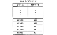
リニアライズメモリ32に制御データを格納する場合、可変遅延回路34に全ての制御データを順次供給し、それぞれの制御データに対して可変遅延回路34が生じる遅延量を測定する。そして、例えば10ps毎に与えられる遅延設定値に最も適した遅延を生じさせることのできる制御データを抽出する。本例においては、遅延設定値0ps、10ps、20ps、30ps、40ps、・・・に対して、制御データ#0、#4、#9、#15、#19、・・・がそれぞれ抽出される。リニアライズメモリ32は、これらの遅延設定値と制御データとを対応付けて格納する。
When control data is stored in the linearized memory 32, all control data is sequentially supplied to the variable delay circuit 34, and the amount of delay generated by the variable delay circuit 34 is measured for each control data. Then, for example, control data capable of causing a delay most suitable for a delay setting value given every 10 ps is extracted. In this example,
図4は、リニアライズメモリ32が格納するデータの一例を示す図である。前述したように、リニアライズメモリ32は、遅延設定値と制御データとを対応付けて格納する。本例においては、リニアライズメモリ32のそれぞれのアドレスがそれぞれの遅延設定値に対応する。スキュー調整部46は、リニアライズメモリ32が格納する上記制御データを調整することにより、測定したスキューを調整する。 FIG. 4 is a diagram illustrating an example of data stored in the linearized memory 32. As described above, the linearization memory 32 stores the delay setting value and the control data in association with each other. In this example, each address of the linearized memory 32 corresponds to each delay setting value. The skew adjustment unit 46 adjusts the measured skew by adjusting the control data stored in the linearize memory 32.
例えば、スキュー調整部46は、第1可変遅延回路36−1及び第2可変遅延回路36−2が出力する信号のいずれの位相が早いかを検出し、位相が早い信号を出力する第1可変遅延回路36−1又は第2可変遅延回路36−2に対応する、第1リニアライズメモリ32−1又は第2リニアライズメモリ32−2に、それぞれの遅延設定値に、測定したスキューに応じた値を加えた設定値に対応づけて格納されるべき制御データを、それぞれの当該遅延設定値に対応づけて格納する。 For example, the skew adjustment unit 46 detects which phase of the signal output from the first variable delay circuit 36-1 and the second variable delay circuit 36-2 is earlier, and outputs a signal having an earlier phase. The first linearized memory 32-1 or the second linearized memory 32-2 corresponding to the delay circuit 36-1 or the second variable delay circuit 36-2 has a delay setting value corresponding to the measured skew. Control data to be stored in association with the set value to which the value is added is stored in association with each delay setting value.
本例においては、第2可変遅延回路36−2が出力する信号の位相が早い場合における、第2リニアライズメモリ32−2が格納する制御データの調整について説明する。 In this example, adjustment of control data stored in the second linearized memory 32-2 when the phase of the signal output from the second variable delay circuit 36-2 is early will be described.
図5は、第2可変遅延回路36−2に与えられる制御データと、第2可変遅延回路36−2における実際の遅延量との関係の一例を示す図である。まず、スキュー調整部46は、第1可変遅延回路36−1及び第2可変遅延回路36−2における遅延設定値をそれぞれ最小の遅延設定値にしたときの、第1セット信号と第2セット信号とのスキューを測定する。 FIG. 5 is a diagram illustrating an example of the relationship between the control data given to the second variable delay circuit 36-2 and the actual delay amount in the second variable delay circuit 36-2. First, the skew adjustment unit 46 sets the first set signal and the second set signal when the delay setting values in the first variable delay circuit 36-1 and the second variable delay circuit 36-2 are set to the minimum delay setting values, respectively. And measure the skew.
そして、スキュー調整部46は、出力する信号の位相が遅い第1可変遅延回路36−1に対しては、対応する第1リニアライズメモリ32−1に、図3及び図4において説明した方法で制御データを格納する。 Then, the skew adjustment unit 46 applies the first variable delay circuit 36-1 whose output signal is slow in phase to the corresponding first linearization memory 32-1 by the method described with reference to FIGS. 3 and 4. Stores control data.
次に、スキュー調整部46は、第2可変遅延回路36−2に対しても、全ての制御データを順次供給し、それぞれの制御データに対する実際の遅延量を測定する。そして、与えられるそれぞれの遅延設定値に、測定したスキューに応じたオフセット値Xを加えた設定値に対応づけて格納されるべき制御データを抽出する。本例においては、それぞれの遅延設定値0ps、10ps、20ps、30ps、40ps、・・・に対して、制御データ#30、#35、#41、#44、#49、・・・が抽出される。
Next, the skew adjustment unit 46 sequentially supplies all the control data also to the second variable delay circuit 36-2, and measures the actual delay amount for each control data. Then, control data to be stored in association with a set value obtained by adding an offset value X corresponding to the measured skew to each given delay set value is extracted. In this example,
そしてスキュー調整部46は、オフセット値Xを加えない遅延設定値に対応付けて、抽出した制御データをそれぞれ第2リニアライズメモリ32−2に格納する。 Then, the skew adjustment unit 46 stores the extracted control data in the second linearized memory 32-2 in association with the delay setting value to which the offset value X is not added.
図6は、第2リニアライズメモリ32−2が格納するデータの一例を示す図である。前述したように、第2リニアライズメモリ32−2は、遅延設定値と、スキューに応じた制御データとを対応付けて格納する。このような動作により、第1セット信号と第2セット信号との間のスキューを調整することができる。また、前述したように、遅延設定値の分解能は可変遅延回路34が実際に生成する遅延量の分解能より大きいが、本例におけるタイミング発生器20は、可変遅延回路34が実際に生成する遅延量から、スキューを調整するための遅延量を選択するため、可変遅延回路34の実際の遅延分解能まで、当該スキューを低減することができる。
FIG. 6 is a diagram illustrating an example of data stored in the second linearized memory 32-2. As described above, the second linearized memory 32-2 stores the delay setting value and the control data corresponding to the skew in association with each other. By such an operation, the skew between the first set signal and the second set signal can be adjusted. Further, as described above, the resolution of the delay set value is larger than the resolution of the delay amount actually generated by the variable delay circuit 34. However, the
また、タイミング発生器20は、スキュー調整部46が測定したスキューを、第1可変遅延回路36−1及び第2可変遅延回路36−2の遅延設定値の分解能で除算したときの商を格納するスキューレジスタ(28−1、28−2、図2参照)と、スキューレジスタ(28−1、28−2)が格納した値を、第1可変遅延回路36−1又は第2可変遅延回路36−2のうち位相が早い信号を出力するほうに与えられるべき遅延設定値に加算する加算部(30−1、30−2、図2参照)とを備える。
Further, the
この場合、スキュー調整部46は、それぞれの遅延設定値に、測定したスキューを第1可変遅延回路36−1及び第2可変遅延回路36−2の遅延設定値の分解能で除算したときの余りを加えた設定値に対応づけて格納されるべき制御データを、それぞれの当該遅延設定値に対応づけて、位相が早い信号を出力する第1可変遅延回路36−1又は第2可変遅延回路36−2に対応する第1リニアライズメモリ32−1又は第2リニアライズメモリ32−2に格納する。このような構成によれば、遅延設定値の分解能以上のスキューを、可変遅延回路34に与える遅延設定値を制御することにより容易に除去し、遅延設定値の分解能より小さいスキューを、上述した方法で低減することができる。 In this case, the skew adjustment unit 46 divides the remainder when each measured skew is divided by the resolution of the delay setting values of the first variable delay circuit 36-1 and the second variable delay circuit 36-2. The first variable delay circuit 36-1 or the second variable delay circuit 36-that outputs a signal having an early phase by associating the control data to be stored in association with the added set value with each delay set value. 2 is stored in the first linearized memory 32-1 or the second linearized memory 32-2. According to such a configuration, the skew equal to or higher than the resolution of the delay setting value can be easily removed by controlling the delay setting value given to the variable delay circuit 34, and the skew smaller than the resolution of the delay setting value can be reduced by the method described above. Can be reduced.
また、スキュー調整部46は、所定の期間内で、ループ経路60を通過する第1セット信号又は第2セット信号の前縁又は後縁を計数することにより、それぞれのループ周期を測定する。図2に示したように、ループ経路60には、パルス幅を調整するための複数のパルサー(48、52、54、56、58)が設けられている。このような場合、それぞれのセット信号の前縁を基準とするか、後縁を基準とするかで、第1セット信号及び第2セット信号との間のスキューが変化してみえる。
Further, the skew adjustment unit 46 measures each loop period by counting the leading edge or the trailing edge of the first set signal or the second set signal passing through the
第1セット信号と第2セット信号との間のスキューをいずれのエッジを基準として測定するべきかは、タイミング発生器20が生成するタイミング信号の用途によって定まる。図2に示すように、セットリセットラッチ22にセット信号を入力する場合、セットリセットラッチ22は通常、信号の前縁に応じて動作するため、セット信号の前縁を基準としてスキューを測定する必要がある。また、判定器14において、出力信号の値を検出するストローブ信号として用いる場合、コンパレータは通常信号の後縁に応じて動作するため、セット信号の後縁を基準としてスキューを測定する必要がある。
Which edge is used as a reference for measuring the skew between the first set signal and the second set signal depends on the use of the timing signal generated by the
ループ経路60は、ループ経路60を通過する信号と、第1セット信号及び第2セット信号の前縁又は後縁のいずれを基準としてスキューを測定するかを示すエッジ制御信号との排他論理和を出力する排他論理和回路50を有しており、エッジ制御信号に応じて、第1セット信号及び前記第2セット信号を非反転で出力するか、又は反転して出力するかを切り替える。このような構成により、タイミング信号の用途に応じて、セット信号の前縁又は後縁のいずれを基準としてスキューを調整するかを制御できる。エッジ制御信号は、例えばパターン発生器10が供給してよい。
The
図7は、図2に関連して説明したタイミング発生器20において、第1セット信号と第2セット信号との間のスキューを調整するスキュー調整方法の概要を示すフローチャートである。当該スキュー調整方法は、図2から図6において説明した方法で、当該スキューを調整する。
FIG. 7 is a flowchart showing an outline of a skew adjustment method for adjusting the skew between the first set signal and the second set signal in the
まず、第1セット信号のループ周期を測定する(第1周期算出段階S300)。次に、第2セット信号のループ周期を測定する(第2周期算出段階S302)。そして、第1周期算出段階S300において算出したループ周期と、第2周期算出段階S302において算出したループ周期との差分に基づいて、第1セット信号と第2セット信号との間のスキューを算出する(スキュー測定段階S304)。 First, the loop period of the first set signal is measured (first period calculation step S300). Next, the loop period of the second set signal is measured (second period calculation step S302). Then, the skew between the first set signal and the second set signal is calculated based on the difference between the loop period calculated in the first period calculating step S300 and the loop period calculated in the second period calculating step S302. (Skew measurement step S304).
そして、位相が進んでいるセット信号に対応するリニアライズメモリ32に、それぞれの遅延設定値に当該スキューに応じた値を加算し、加算した設定値と対応する制御データを、当該遅延設定値に対応付けて格納する(スキュー調整段階S306)。このような方法により、スキューを精度よく調整することができる。 Then, a value corresponding to the skew is added to each delay setting value to the linearized memory 32 corresponding to the set signal whose phase is advanced, and the control data corresponding to the added setting value is set as the delay setting value. The data is stored in association with each other (skew adjustment step S306). By such a method, the skew can be adjusted with high accuracy.
以上、本発明を実施の形態を用いて説明したが、本発明の技術的範囲は上記実施の形態に記載の範囲には限定されない。上記実施の形態に、多様な変更または改良を加えることが可能であることが当業者に明らかである。その様な変更または改良を加えた形態も本発明の技術的範囲に含まれ得ることが、特許請求の範囲の記載から明らかである。 As mentioned above, although this invention was demonstrated using embodiment, the technical scope of this invention is not limited to the range as described in the said embodiment. It will be apparent to those skilled in the art that various modifications or improvements can be added to the above-described embodiment. It is apparent from the scope of the claims that the embodiments added with such changes or improvements can be included in the technical scope of the present invention.
以上から明らかなように、本発明によれば、消費電力が小さいタイミング発生器を提供することができる。また、インターリーブ方式のタイミング発生器において、インターリーブする信号間のスキューを精度よく調整することができる。 As is apparent from the above, according to the present invention, a timing generator with low power consumption can be provided. Further, in an interleaved timing generator, the skew between interleaved signals can be adjusted with high accuracy.
10・・・パターン発生器、12・・・波形成形器、14・・・判定器、20・・・タイミング発生器、22・・・セットリセットラッチ、24・・・セット部、26・・・リセット部、28・・・スキューレジスタ、30・・・加算器、32・・・リニアライズメモリ、34・・・論理積回路、36−1・・・第1可変遅延回路、36−2・・・第2可変遅延回路、38・・・パルサー、40・・・論理和回路、42・・・論理積回路、44・・・第3可変遅延回路、46・・・スキュー調整部、48・・・パルサー、50・・・排他論理和回路、52、54、56、58・・・パルサー、60・・・ループ経路、100・・・試験装置、200・・・電子デバイス、400・・・従来のタイミング発生器、410・・・セットリセットラッチ、420・・・セット回路、430・・・リセット回路、440・・・位相制御用可変遅延回路、450・・・スキュー調整用可変遅延回路、460・・・論理和回路
DESCRIPTION OF
Claims (9)
与えられるセット信号に応じて前記タイミング信号の立ち上がりエッジを生成し、与えられるリセット信号に応じて前記タイミング信号の立ち下がりエッジを生成するセットリセットラッチと、
前記セットリセットラッチに、前記セット信号を供給するセット部と、
前記セットリセットラッチに、前記リセット信号を供給するリセット部と、
前記セット信号のスキューを調整するスキュー調整部と、
を備え、
前記セット部は、
与えられる基準クロックを遅延させた第1セット信号を出力する第1可変遅延回路と、
与えられる基準クロックを遅延させ、前記第1セット信号と位相が異なる第2セット信号を出力する第2可変遅延回路と、
前記第1セット信号と前記第2セット信号との論理和を算出し、前記セット信号を生成する論理和回路と、
前記論理和回路が出力する前記セット信号を遅延させ、前記セット信号と前記リセット信号との間のスキューを調整する第3可変遅延回路と
を有し、
前記スキュー調整部は、前記第1可変遅延回路を介してループさせた前記第1セット信号のループ周期、および前記第2可変遅延回路を介してループさせた前記第2セット信号のループ周期をそれぞれ測定して、前記第1セット信号と前記第2セット信号との間のスキューを算出し、算出した前記スキューに基づいて、前記第1可変遅延回路又は前記第2可変遅延回路における遅延量を制御するタイミング発生器。 A timing generator for generating a timing signal having a predetermined period;
A set reset latch that generates a rising edge of the timing signal in response to a given set signal and generates a falling edge of the timing signal in response to a given reset signal;
A set unit for supplying the set signal to the set reset latch;
A reset unit for supplying the reset signal to the set reset latch;
A skew adjustment unit for adjusting the skew of the set signal;
With
The set part is
A first variable delay circuit for outputting a first set signal obtained by delaying a given reference clock;
A second variable delay circuit for delaying a given reference clock and outputting a second set signal having a phase different from that of the first set signal;
A logical sum circuit for calculating a logical sum of the first set signal and the second set signal and generating the set signal;
A third variable delay circuit that delays the set signal output by the OR circuit and adjusts a skew between the set signal and the reset signal ;
The skew adjustment unit respectively sets a loop period of the first set signal looped through the first variable delay circuit and a loop period of the second set signal looped through the second variable delay circuit. Measure and calculate a skew between the first set signal and the second set signal, and control a delay amount in the first variable delay circuit or the second variable delay circuit based on the calculated skew the timing generator that.
前記論理和回路が出力する前記セット信号を、前記信号入力部に前記基準クロックとして帰還入力するループ経路と
を更に備え、
前記スキュー調整部は、前記第1可変遅延回路が前記第1セット信号を出力するタイミングを測定する場合に前記セット信号が前記ループ経路を通過するループ周期と、前記第2可変遅延回路が前記第2セット信号を出力するタイミングを測定する場合に前記セット信号が前記ループ経路を通過するループ周期との差分に基づいて、前記第1セット信号と前記第2セット信号との間のスキューを算出する
請求項1に記載のタイミング発生器。 Receiving the reference clock and stopping the input of the reference clock to the second variable delay circuit when measuring the timing at which the first variable delay circuit outputs the first set signal; A signal input unit for stopping the input of the reference clock to the first variable delay circuit when measuring the timing of outputting the second set signal;
A loop path for feeding back the set signal output from the OR circuit as a reference clock to the signal input unit;
The skew adjustment unit includes a loop period in which the set signal passes through the loop path when the timing at which the first variable delay circuit outputs the first set signal is measured, and the second variable delay circuit includes the first variable delay circuit. When measuring the timing of outputting two set signals, the skew between the first set signal and the second set signal is calculated based on the difference from the loop period in which the set signal passes through the loop path. The timing generator according to claim 1 .
与えられる遅延設定値に応じて前記第2可変遅延回路を制御するための制御データを、それぞれの前記遅延設定値に対応づけて格納する第2リニアライズメモリと
を更に備え、
前記スキュー調整部は、
前記第1リニアライズメモリ及び前記第2リニアライズメモリが格納する前記制御データを、算出した前記スキューに基づいて調整する
請求項1または2に記載のタイミング発生器。 A first linearized memory for storing control data for controlling the first variable delay circuit in accordance with a given delay setting value in association with each of the delay setting values;
A second linearized memory that stores control data for controlling the second variable delay circuit in accordance with the given delay setting value in association with each of the delay setting values;
The skew adjustment unit
The timing generator according to claim 1 or 2, wherein the first linearization memory and the second linearization memory is the control data to be stored is adjusted on the basis of the calculated skew.
前記第1リニアライズメモリ及び前記第2リニアライズメモリが格納する前記制御データを、測定した前記スキューに基づいて調整する
請求項3に記載のタイミング発生器。 The skew adjustment unit calculates a skew between the first set signal and the second set signal when a delay setting value in the first variable delay circuit and the second variable delay circuit is set to a minimum delay setting value. And
The timing generator according to claim 3 , wherein the control data stored in the first linearized memory and the second linearized memory is adjusted based on the measured skew.
請求項4に記載のタイミング発生器。 The skew adjustment unit detects which phase of the signal output from the first variable delay circuit and the second variable delay circuit is earlier, and outputs the signal having the earlier phase or the first variable delay circuit or the second variable delay circuit. 2 stored in the first linearized memory or the second linearized memory corresponding to the variable delay circuit in association with a set value obtained by adding a value corresponding to the calculated skew to the delay set value. The timing generator according to claim 4 , wherein the control data to be stored is stored in association with each delay setting value.
前記スキューレジスタが格納した値を、位相が早い信号を出力する前記第1可変遅延回路又は前記第2可変遅延回路に与えられるべき前記遅延設定値に加算する加算部と
を更に備え、
前記スキュー調整部は、それぞれの前記遅延設定値に、算出した前記スキューを前記第1可変遅延回路及び前記第2可変遅延回路の前記遅延設定値の分解能で除算したときの余りを加えた設定値に対応づけて格納されるべき前記制御データを、それぞれの当該遅延設定値に対応づけて、位相が早い信号を出力する前記第1可変遅延回路又は前記第2可変遅延回路に対応する前記第1リニアライズメモリ又は前記第2リニアライズメモリに格納する
請求項5に記載のタイミング発生器。 A skew register that stores a quotient obtained by dividing the skew measured by the skew adjustment unit by the resolution of the delay setting value of the first variable delay circuit and the second variable delay circuit;
An addition unit for adding the value stored in the skew register to the delay setting value to be given to the first variable delay circuit or the second variable delay circuit that outputs a signal having an early phase;
The skew adjustment unit is a setting value obtained by adding a remainder when the calculated skew is divided by the resolution of the delay setting value of the first variable delay circuit and the second variable delay circuit to each delay setting value. The control data to be stored in association with the first variable delay circuit or the second variable delay circuit that outputs a signal having an early phase in association with each delay setting value. The timing generator according to claim 5 , wherein the timing generator is stored in a linearized memory or the second linearized memory.
請求項2に記載のタイミング発生器。 In response to an edge control signal provided in the loop path and indicating whether the skew is calculated based on a leading edge or a trailing edge of the first set signal and the second set signal, the first set signal and The timing generator according to claim 2, further comprising an exclusive OR circuit that switches whether the second set signal is output non-inverted or inverted and output.
前記電子デバイスを試験するための試験パターンを生成するパターン生成器と、
所望の周期のタイミング信号を生成するタイミング発生器と、
前記試験パターン及び前記タイミング信号に基づいて、前記電子デバイスに入力する試験信号を生成する波形成形器と、
前記電子デバイスが出力する出力信号に基づいて、前記電子デバイスの良否を判定する判定器と
を備え、
前記タイミング発生器は、
与えられるセット信号に応じて前記タイミング信号の立ち上がりエッジを生成し、与えられるリセット信号に応じて前記タイミング信号の立ち下がりエッジを生成するセットリセットラッチと、
前記セットリセットラッチに、前記セット信号を供給するセット部と、
前記セットリセットラッチに、前記リセット信号を供給するリセット部と
を有し、
前記セット部は、
与えられる基準クロックを遅延させた第1セット信号を出力する第1可変遅延回路と、
与えられる基準クロックを遅延させ、前記第1セット信号と位相が異なる第2セット信号を出力する第2可変遅延回路と、
前記第1セット信号と前記第2セット信号との論理和を算出し、前記セット信号を生成する論理和回路と、
前記論理和回路が出力する前記セット信号を遅延させ、前記セット信号と前記リセット信号との間のスキューを調整する第3可変遅延回路と
を含む試験装置。 A test apparatus for testing an electronic device,
A pattern generator for generating a test pattern for testing the electronic device;
A timing generator for generating a timing signal having a desired period;
A waveform shaper that generates a test signal to be input to the electronic device based on the test pattern and the timing signal;
A determination unit for determining whether the electronic device is good or not based on an output signal output from the electronic device;
The timing generator is
A set reset latch that generates a rising edge of the timing signal in response to a given set signal and generates a falling edge of the timing signal in response to a given reset signal;
A set unit for supplying the set signal to the set reset latch;
A reset unit for supplying the reset signal to the set reset latch;
The set part is
A first variable delay circuit for outputting a first set signal obtained by delaying a given reference clock;
A second variable delay circuit for delaying a given reference clock and outputting a second set signal having a phase different from that of the first set signal;
A logical sum circuit for calculating a logical sum of the first set signal and the second set signal and generating the set signal;
And a third variable delay circuit that delays the set signal output from the OR circuit and adjusts a skew between the set signal and the reset signal.
第2信号を出力する第2可変遅延回路と、
与えられる遅延設定値に応じて前記第1可変遅延回路を制御するための制御データを、それぞれの前記遅延設定値に対応づけて格納する第1リニアライズメモリと、
与えられる遅延設定値に応じて前記第2可変遅延回路を制御するための制御データを、それぞれの前記遅延設定値に対応づけて格納する第2リニアライズメモリと
前記第1信号と前記第2信号との論理和を出力する論理和回路と
を備えるタイミング発生器において、前記第1信号と前記第2信号との間のスキューを調整するスキュー調整方法であって、
前記第1信号を前記論理和回路を介して前記第1可変遅延回路に帰還入力し、前記論理和回路が前記第1信号を出力する周期を算出する第1周期算出段階と、
前記第2信号を前記論理和回路を介して前記第2可変遅延回路に帰還入力し、前記論理和回路が前記第2信号を出力する周期を算出する第2周期算出段階と、
前記第1周期算出段階において算出した周期と、前記第2周期算出段階において算出した周期との差分に基づいて、前記第1信号と前記第2信号との間のスキューを算出するスキュー測定段階と、
それぞれの前記遅延設定値に前記スキュー測定段階において測定した前記スキューに応じた値を加えた設定値に対応づけて格納されるべき前記制御データを、当該遅延設定値に対応づけて、前記第1リニアライズメモリ又は前記第2リニアライズメモリのいずれかに格納するスキュー調整段階と
を備えるスキュー調整方法。 A first variable delay circuit for outputting a first signal;
A second variable delay circuit for outputting a second signal;
A first linearized memory for storing control data for controlling the first variable delay circuit in accordance with a given delay setting value in association with each of the delay setting values;
A second linearized memory for storing control data for controlling the second variable delay circuit in accordance with a given delay setting value in association with each delay setting value; the first signal; and the second signal In a timing generator comprising a logical sum circuit that outputs a logical sum of the first and second signals, a skew adjustment method for adjusting a skew between the first signal and the second signal,
A first period calculating step of feeding back the first signal to the first variable delay circuit via the OR circuit and calculating a period in which the OR circuit outputs the first signal;
A second period calculating step of feeding back the second signal to the second variable delay circuit through the OR circuit and calculating a period in which the OR circuit outputs the second signal;
A skew measuring step of calculating a skew between the first signal and the second signal based on a difference between the cycle calculated in the first cycle calculating step and the cycle calculated in the second cycle calculating step; ,
The control data to be stored in association with a set value obtained by adding a value corresponding to the skew measured in the skew measurement step to each delay set value is associated with the delay set value, and the first A skew adjustment method comprising: a skew adjustment step of storing in either the linearized memory or the second linearized memory.
Priority Applications (2)
| Application Number | Priority Date | Filing Date | Title |
|---|---|---|---|
| JP2004235635A JP4477450B2 (en) | 2004-08-12 | 2004-08-12 | Timing generator, test apparatus, and skew adjustment method |
| US11/197,118 US7203611B2 (en) | 2004-08-12 | 2005-08-04 | Timing generator, test apparatus and skew adjusting method |
Applications Claiming Priority (1)
| Application Number | Priority Date | Filing Date | Title |
|---|---|---|---|
| JP2004235635A JP4477450B2 (en) | 2004-08-12 | 2004-08-12 | Timing generator, test apparatus, and skew adjustment method |
Publications (2)
| Publication Number | Publication Date |
|---|---|
| JP2006054731A JP2006054731A (en) | 2006-02-23 |
| JP4477450B2 true JP4477450B2 (en) | 2010-06-09 |
Family
ID=35910908
Family Applications (1)
| Application Number | Title | Priority Date | Filing Date |
|---|---|---|---|
| JP2004235635A Expired - Fee Related JP4477450B2 (en) | 2004-08-12 | 2004-08-12 | Timing generator, test apparatus, and skew adjustment method |
Country Status (2)
| Country | Link |
|---|---|
| US (1) | US7203611B2 (en) |
| JP (1) | JP4477450B2 (en) |
Families Citing this family (10)
| Publication number | Priority date | Publication date | Assignee | Title |
|---|---|---|---|---|
| US7024324B2 (en) * | 2004-05-27 | 2006-04-04 | Intel Corporation | Delay element calibration |
| JP4895551B2 (en) * | 2005-08-10 | 2012-03-14 | 株式会社アドバンテスト | Test apparatus and test method |
| WO2007138814A1 (en) * | 2006-05-26 | 2007-12-06 | Advantest Corporation | Testing apparatus and test module |
| US7747972B2 (en) * | 2006-12-07 | 2010-06-29 | Infineon Technologies Ag | Methods and apparatuses for timing analysis of electronic circuits |
| CN101978485B (en) | 2008-03-26 | 2012-07-04 | 爱德万测试株式会社 | Probe wafer, probe device, and testing system |
| KR101239121B1 (en) | 2008-06-02 | 2013-03-11 | 가부시키가이샤 어드밴티스트 | Testing device, transmission circuit, testing device control method and transmission circuit control method |
| KR101285287B1 (en) | 2009-06-22 | 2013-07-11 | 가부시키가이샤 어드밴티스트 | Timing generator and tester |
| JP5549474B2 (en) * | 2010-08-20 | 2014-07-16 | 富士通セミコンダクター株式会社 | Integrated circuit |
| US8856578B2 (en) | 2010-08-20 | 2014-10-07 | Fujitsu Semiconductor Limited | Integrated circuit device including skew adjustment circuit and skew adjustment method |
| US10115480B1 (en) * | 2017-07-03 | 2018-10-30 | Qualcomm Incorporated | Double data rate synchronous dynamic random access memory (“DDR SDRAM”) data strobe signal calibration |
Family Cites Families (3)
| Publication number | Priority date | Publication date | Assignee | Title |
|---|---|---|---|---|
| JPH04268811A (en) * | 1991-02-22 | 1992-09-24 | Yokogawa Hewlett Packard Ltd | Timing generator |
| JP3545163B2 (en) * | 1997-04-10 | 2004-07-21 | パイオニア株式会社 | Signal conversion device and digital information recording device |
| DE10080254B4 (en) * | 1999-01-08 | 2004-12-09 | Advantest Corp. | Waveform generating device and semiconductor test device |
-
2004
- 2004-08-12 JP JP2004235635A patent/JP4477450B2/en not_active Expired - Fee Related
-
2005
- 2005-08-04 US US11/197,118 patent/US7203611B2/en not_active Expired - Fee Related
Also Published As
| Publication number | Publication date |
|---|---|
| US7203611B2 (en) | 2007-04-10 |
| US20060041772A1 (en) | 2006-02-23 |
| JP2006054731A (en) | 2006-02-23 |
Similar Documents
| Publication | Publication Date | Title |
|---|---|---|
| US7203611B2 (en) | Timing generator, test apparatus and skew adjusting method | |
| US7406646B2 (en) | Multi-strobe apparatus, testing apparatus, and adjusting method | |
| US6996032B2 (en) | BIST circuit for measuring path delay in an IC | |
| US7782064B2 (en) | Test apparatus and test module | |
| US7216271B2 (en) | Testing apparatus and a testing method | |
| TWI404954B (en) | Test apparatus and test method for synchronizing test signal | |
| CN1938788A (en) | Test apparatus, phase adjusting method and memory controller | |
| JP5577776B2 (en) | Memory control apparatus and mask timing control method | |
| US6574579B1 (en) | Waveform generating device | |
| JP4469753B2 (en) | Test equipment | |
| JP4394788B2 (en) | Delay time judgment device | |
| US8436604B2 (en) | Measuring apparatus, parallel measuring apparatus, testing apparatus and electronic device | |
| JP4109951B2 (en) | Multi-strobe device, test device, and adjustment method | |
| EP1653239B1 (en) | Test apparatus with waveform formatter | |
| JP3588235B2 (en) | Semiconductor test equipment | |
| JPWO2007091413A1 (en) | Change point detection circuit, jitter measurement apparatus, and test apparatus | |
| JP2002139556A (en) | Semiconductor testing apparatus | |
| JP4162810B2 (en) | Timing phase calibration method and apparatus for semiconductor device test equipment | |
| JP2965049B2 (en) | Timing generator | |
| JP4669258B2 (en) | Timing generator and test apparatus | |
| JP2008039764A (en) | Signal output circuit for outputting signal, and testing device equipped with the signal output circuit | |
| JP4412775B2 (en) | Delay signal generating apparatus and method for adjusting delay amount thereof | |
| US7092827B2 (en) | Edge placement accuracy of signals generated by test equipment | |
| JP3216608B2 (en) | Semiconductor test apparatus and storage medium storing program | |
| JPH06265597A (en) | Test equipment for semiconductor integrated circuit |
Legal Events
| Date | Code | Title | Description |
|---|---|---|---|
| A621 | Written request for application examination |
Free format text: JAPANESE INTERMEDIATE CODE: A621 Effective date: 20070223 |
|
| A977 | Report on retrieval |
Free format text: JAPANESE INTERMEDIATE CODE: A971007 Effective date: 20090616 |
|
| A131 | Notification of reasons for refusal |
Free format text: JAPANESE INTERMEDIATE CODE: A131 Effective date: 20090818 |
|
| A521 | Request for written amendment filed |
Free format text: JAPANESE INTERMEDIATE CODE: A523 Effective date: 20091015 |
|
| TRDD | Decision of grant or rejection written | ||
| A01 | Written decision to grant a patent or to grant a registration (utility model) |
Free format text: JAPANESE INTERMEDIATE CODE: A01 Effective date: 20100309 |
|
| A01 | Written decision to grant a patent or to grant a registration (utility model) |
Free format text: JAPANESE INTERMEDIATE CODE: A01 |
|
| A61 | First payment of annual fees (during grant procedure) |
Free format text: JAPANESE INTERMEDIATE CODE: A61 Effective date: 20100311 |
|
| R150 | Certificate of patent or registration of utility model |
Free format text: JAPANESE INTERMEDIATE CODE: R150 |
|
| FPAY | Renewal fee payment (event date is renewal date of database) |
Free format text: PAYMENT UNTIL: 20130319 Year of fee payment: 3 |
|
| FPAY | Renewal fee payment (event date is renewal date of database) |
Free format text: PAYMENT UNTIL: 20130319 Year of fee payment: 3 |
|
| FPAY | Renewal fee payment (event date is renewal date of database) |
Free format text: PAYMENT UNTIL: 20130319 Year of fee payment: 3 |
|
| FPAY | Renewal fee payment (event date is renewal date of database) |
Free format text: PAYMENT UNTIL: 20140319 Year of fee payment: 4 |
|
| LAPS | Cancellation because of no payment of annual fees |