JP4475813B2 - Holographic illumination device - Google Patents
Holographic illumination device Download PDFInfo
- Publication number
- JP4475813B2 JP4475813B2 JP2000570617A JP2000570617A JP4475813B2 JP 4475813 B2 JP4475813 B2 JP 4475813B2 JP 2000570617 A JP2000570617 A JP 2000570617A JP 2000570617 A JP2000570617 A JP 2000570617A JP 4475813 B2 JP4475813 B2 JP 4475813B2
- Authority
- JP
- Japan
- Prior art keywords
- light
- hoe
- light source
- image display
- color
- Prior art date
- Legal status (The legal status is an assumption and is not a legal conclusion. Google has not performed a legal analysis and makes no representation as to the accuracy of the status listed.)
- Expired - Lifetime
Links
- 238000005286 illumination Methods 0.000 title claims description 48
- 230000003287 optical effect Effects 0.000 claims description 62
- 238000000034 method Methods 0.000 claims description 24
- 230000008569 process Effects 0.000 claims description 11
- 230000008859 change Effects 0.000 claims description 10
- 239000004973 liquid crystal related substance Substances 0.000 description 103
- 239000004983 Polymer Dispersed Liquid Crystal Substances 0.000 description 96
- 239000000463 material Substances 0.000 description 91
- 230000005684 electric field Effects 0.000 description 47
- 229920000642 polymer Polymers 0.000 description 40
- 239000000178 monomer Substances 0.000 description 34
- 239000004094 surface-active agent Substances 0.000 description 23
- 230000000737 periodic effect Effects 0.000 description 22
- 239000000523 sample Substances 0.000 description 22
- 239000000975 dye Substances 0.000 description 18
- 239000000203 mixture Substances 0.000 description 18
- 230000005540 biological transmission Effects 0.000 description 17
- 230000010287 polarization Effects 0.000 description 15
- WWZKQHOCKIZLMA-UHFFFAOYSA-N octanoic acid Chemical compound CCCCCCCC(O)=O WWZKQHOCKIZLMA-UHFFFAOYSA-N 0.000 description 12
- 239000011521 glass Substances 0.000 description 11
- -1 argon ion Chemical class 0.000 description 10
- 239000003086 colorant Substances 0.000 description 10
- 239000004970 Chain extender Substances 0.000 description 9
- ZMANZCXQSJIPKH-UHFFFAOYSA-N Triethylamine Chemical compound CCN(CC)CC ZMANZCXQSJIPKH-UHFFFAOYSA-N 0.000 description 9
- 230000006870 function Effects 0.000 description 9
- 239000011248 coating agent Substances 0.000 description 8
- 238000000576 coating method Methods 0.000 description 8
- 239000000126 substance Substances 0.000 description 8
- NPKSPKHJBVJUKB-UHFFFAOYSA-N N-phenylglycine Chemical compound OC(=O)CNC1=CC=CC=C1 NPKSPKHJBVJUKB-UHFFFAOYSA-N 0.000 description 7
- OKKJLVBELUTLKV-UHFFFAOYSA-N Methanol Chemical compound OC OKKJLVBELUTLKV-UHFFFAOYSA-N 0.000 description 6
- GSEJCLTVZPLZKY-UHFFFAOYSA-N Triethanolamine Chemical compound OCCN(CCO)CCO GSEJCLTVZPLZKY-UHFFFAOYSA-N 0.000 description 6
- OBETXYAYXDNJHR-UHFFFAOYSA-N alpha-ethylcaproic acid Natural products CCCCC(CC)C(O)=O OBETXYAYXDNJHR-UHFFFAOYSA-N 0.000 description 6
- 238000010276 construction Methods 0.000 description 6
- PJXISJQVUVHSOJ-UHFFFAOYSA-N indium(iii) oxide Chemical compound [O-2].[O-2].[O-2].[In+3].[In+3] PJXISJQVUVHSOJ-UHFFFAOYSA-N 0.000 description 6
- 230000035945 sensitivity Effects 0.000 description 6
- NIXOWILDQLNWCW-UHFFFAOYSA-M acrylate group Chemical group C(C=C)(=O)[O-] NIXOWILDQLNWCW-UHFFFAOYSA-M 0.000 description 5
- XKRFYHLGVUSROY-UHFFFAOYSA-N argon Substances [Ar] XKRFYHLGVUSROY-UHFFFAOYSA-N 0.000 description 5
- 229910052786 argon Inorganic materials 0.000 description 5
- 230000007423 decrease Effects 0.000 description 5
- 238000005516 engineering process Methods 0.000 description 5
- 229910003437 indium oxide Inorganic materials 0.000 description 5
- 230000004048 modification Effects 0.000 description 5
- 238000012986 modification Methods 0.000 description 5
- 238000005191 phase separation Methods 0.000 description 5
- 238000006116 polymerization reaction Methods 0.000 description 5
- 238000002834 transmittance Methods 0.000 description 5
- INQDDHNZXOAFFD-UHFFFAOYSA-N 2-[2-(2-prop-2-enoyloxyethoxy)ethoxy]ethyl prop-2-enoate Chemical compound C=CC(=O)OCCOCCOCCOC(=O)C=C INQDDHNZXOAFFD-UHFFFAOYSA-N 0.000 description 4
- WHNWPMSKXPGLAX-UHFFFAOYSA-N N-Vinyl-2-pyrrolidone Chemical compound C=CN1CCCC1=O WHNWPMSKXPGLAX-UHFFFAOYSA-N 0.000 description 4
- 230000008901 benefit Effects 0.000 description 4
- 230000015572 biosynthetic process Effects 0.000 description 4
- 238000004132 cross linking Methods 0.000 description 4
- 238000013461 design Methods 0.000 description 4
- 239000006185 dispersion Substances 0.000 description 4
- 230000000644 propagated effect Effects 0.000 description 4
- 125000006850 spacer group Chemical group 0.000 description 4
- 239000000758 substrate Substances 0.000 description 4
- RBTBFTRPCNLSDE-UHFFFAOYSA-N 3,7-bis(dimethylamino)phenothiazin-5-ium Chemical compound C1=CC(N(C)C)=CC2=[S+]C3=CC(N(C)C)=CC=C3N=C21 RBTBFTRPCNLSDE-UHFFFAOYSA-N 0.000 description 3
- 239000004971 Cross linker Substances 0.000 description 3
- XQAVYBWWWZMURF-UHFFFAOYSA-N OC(=O)C=C.OC(=O)C=C.OC(=O)C=C.OC(=O)C=C.OC(=O)C=C.OCC(CO)(CO)CO Chemical compound OC(=O)C=C.OC(=O)C=C.OC(=O)C=C.OC(=O)C=C.OC(=O)C=C.OCC(CO)(CO)CO XQAVYBWWWZMURF-UHFFFAOYSA-N 0.000 description 3
- 238000004873 anchoring Methods 0.000 description 3
- 239000002131 composite material Substances 0.000 description 3
- 238000010168 coupling process Methods 0.000 description 3
- UWBXIFCTIZXXLS-UHFFFAOYSA-L disodium;2,3,4,5-tetrachloro-6-(2,4,5,7-tetraiodo-3-oxido-6-oxoxanthen-9-yl)benzoate Chemical compound [Na+].[Na+].[O-]C(=O)C1=C(Cl)C(Cl)=C(Cl)C(Cl)=C1C1=C2C=C(I)C(=O)C(I)=C2OC2=C(I)C([O-])=C(I)C=C21 UWBXIFCTIZXXLS-UHFFFAOYSA-L 0.000 description 3
- YQGOJNYOYNNSMM-UHFFFAOYSA-N eosin Chemical compound [Na+].OC(=O)C1=CC=CC=C1C1=C2C=C(Br)C(=O)C(Br)=C2OC2=C(Br)C(O)=C(Br)C=C21 YQGOJNYOYNNSMM-UHFFFAOYSA-N 0.000 description 3
- 239000011159 matrix material Substances 0.000 description 3
- 229960000907 methylthioninium chloride Drugs 0.000 description 3
- VLKZOEOYAKHREP-UHFFFAOYSA-N n-Hexane Chemical compound CCCCCC VLKZOEOYAKHREP-UHFFFAOYSA-N 0.000 description 3
- 238000002360 preparation method Methods 0.000 description 3
- 230000004044 response Effects 0.000 description 3
- 239000007858 starting material Substances 0.000 description 3
- VNQXSTWCDUXYEZ-UHFFFAOYSA-N 1,7,7-trimethylbicyclo[2.2.1]heptane-2,3-dione Chemical compound C1CC2(C)C(=O)C(=O)C1C2(C)C VNQXSTWCDUXYEZ-UHFFFAOYSA-N 0.000 description 2
- TXBCBTDQIULDIA-UHFFFAOYSA-N 2-[[3-hydroxy-2,2-bis(hydroxymethyl)propoxy]methyl]-2-(hydroxymethyl)propane-1,3-diol Chemical compound OCC(CO)(CO)COCC(CO)(CO)CO TXBCBTDQIULDIA-UHFFFAOYSA-N 0.000 description 2
- IICCLYANAQEHCI-UHFFFAOYSA-N 4,5,6,7-tetrachloro-3',6'-dihydroxy-2',4',5',7'-tetraiodospiro[2-benzofuran-3,9'-xanthene]-1-one Chemical compound O1C(=O)C(C(=C(Cl)C(Cl)=C2Cl)Cl)=C2C21C1=CC(I)=C(O)C(I)=C1OC1=C(I)C(O)=C(I)C=C21 IICCLYANAQEHCI-UHFFFAOYSA-N 0.000 description 2
- HHPCNRKYVYWYAU-UHFFFAOYSA-N 4-cyano-4'-pentylbiphenyl Chemical group C1=CC(CCCCC)=CC=C1C1=CC=C(C#N)C=C1 HHPCNRKYVYWYAU-UHFFFAOYSA-N 0.000 description 2
- 241000282461 Canis lupus Species 0.000 description 2
- IMNFDUFMRHMDMM-UHFFFAOYSA-N N-Heptane Chemical compound CCCCCCC IMNFDUFMRHMDMM-UHFFFAOYSA-N 0.000 description 2
- 206010034972 Photosensitivity reaction Diseases 0.000 description 2
- XUIMIQQOPSSXEZ-UHFFFAOYSA-N Silicon Chemical compound [Si] XUIMIQQOPSSXEZ-UHFFFAOYSA-N 0.000 description 2
- DAKWPKUUDNSNPN-UHFFFAOYSA-N Trimethylolpropane triacrylate Chemical compound C=CC(=O)OCC(CC)(COC(=O)C=C)COC(=O)C=C DAKWPKUUDNSNPN-UHFFFAOYSA-N 0.000 description 2
- HVVWZTWDBSEWIH-UHFFFAOYSA-N [2-(hydroxymethyl)-3-prop-2-enoyloxy-2-(prop-2-enoyloxymethyl)propyl] prop-2-enoate Chemical compound C=CC(=O)OCC(CO)(COC(=O)C=C)COC(=O)C=C HVVWZTWDBSEWIH-UHFFFAOYSA-N 0.000 description 2
- 150000001252 acrylic acid derivatives Chemical class 0.000 description 2
- 230000004075 alteration Effects 0.000 description 2
- 238000013459 approach Methods 0.000 description 2
- WPYMKLBDIGXBTP-UHFFFAOYSA-N benzoic acid Chemical compound OC(=O)C1=CC=CC=C1 WPYMKLBDIGXBTP-UHFFFAOYSA-N 0.000 description 2
- 230000001588 bifunctional effect Effects 0.000 description 2
- 229930006711 bornane-2,3-dione Natural products 0.000 description 2
- DBZJJPROPLPMSN-UHFFFAOYSA-N bromoeosin Chemical compound O1C(=O)C2=CC=CC=C2C21C1=CC(Br)=C(O)C(Br)=C1OC1=C(Br)C(O)=C(Br)C=C21 DBZJJPROPLPMSN-UHFFFAOYSA-N 0.000 description 2
- 230000001427 coherent effect Effects 0.000 description 2
- 230000008878 coupling Effects 0.000 description 2
- 238000005859 coupling reaction Methods 0.000 description 2
- 238000009792 diffusion process Methods 0.000 description 2
- 238000009826 distribution Methods 0.000 description 2
- POULHZVOKOAJMA-UHFFFAOYSA-N dodecanoic acid Chemical compound CCCCCCCCCCCC(O)=O POULHZVOKOAJMA-UHFFFAOYSA-N 0.000 description 2
- 150000002148 esters Chemical class 0.000 description 2
- 230000002349 favourable effect Effects 0.000 description 2
- 239000010408 film Substances 0.000 description 2
- GNBHRKFJIUUOQI-UHFFFAOYSA-N fluorescein Chemical compound O1C(=O)C2=CC=CC=C2C21C1=CC=C(O)C=C1OC1=CC(O)=CC=C21 GNBHRKFJIUUOQI-UHFFFAOYSA-N 0.000 description 2
- MNWFXJYAOYHMED-UHFFFAOYSA-N heptanoic acid Chemical compound CCCCCCC(O)=O MNWFXJYAOYHMED-UHFFFAOYSA-N 0.000 description 2
- 230000006698 induction Effects 0.000 description 2
- 239000003999 initiator Substances 0.000 description 2
- 230000010354 integration Effects 0.000 description 2
- 238000002156 mixing Methods 0.000 description 2
- 230000036211 photosensitivity Effects 0.000 description 2
- 229930187593 rose bengal Natural products 0.000 description 2
- 229940081623 rose bengal Drugs 0.000 description 2
- STRXNPAVPKGJQR-UHFFFAOYSA-N rose bengal A Natural products O1C(=O)C(C(=CC=C2Cl)Cl)=C2C21C1=CC(I)=C(O)C(I)=C1OC1=C(I)C(O)=C(I)C=C21 STRXNPAVPKGJQR-UHFFFAOYSA-N 0.000 description 2
- 229910052710 silicon Inorganic materials 0.000 description 2
- 239000010703 silicon Substances 0.000 description 2
- 239000002904 solvent Substances 0.000 description 2
- 239000010409 thin film Substances 0.000 description 2
- 229940096522 trimethylolpropane triacrylate Drugs 0.000 description 2
- LWIHDJKSTIGBAC-UHFFFAOYSA-K tripotassium phosphate Chemical compound [K+].[K+].[K+].[O-]P([O-])([O-])=O LWIHDJKSTIGBAC-UHFFFAOYSA-K 0.000 description 2
- 125000000391 vinyl group Chemical group [H]C([*])=C([H])[H] 0.000 description 2
- 229920002554 vinyl polymer Polymers 0.000 description 2
- QGKMIGUHVLGJBR-UHFFFAOYSA-M (4z)-1-(3-methylbutyl)-4-[[1-(3-methylbutyl)quinolin-1-ium-4-yl]methylidene]quinoline;iodide Chemical compound [I-].C12=CC=CC=C2N(CCC(C)C)C=CC1=CC1=CC=[N+](CCC(C)C)C2=CC=CC=C12 QGKMIGUHVLGJBR-UHFFFAOYSA-M 0.000 description 1
- MYWOJODOMFBVCB-UHFFFAOYSA-N 1,2,6-trimethylphenanthrene Chemical compound CC1=CC=C2C3=CC(C)=CC=C3C=CC2=C1C MYWOJODOMFBVCB-UHFFFAOYSA-N 0.000 description 1
- OZFIGURLAJSLIR-UHFFFAOYSA-N 1-ethenyl-2h-pyridine Chemical compound C=CN1CC=CC=C1 OZFIGURLAJSLIR-UHFFFAOYSA-N 0.000 description 1
- HYKNZBZFSXYENS-UHFFFAOYSA-N 2-anilinoacetic acid Chemical compound OC(=O)CNC1=CC=CC=C1.OC(=O)CNC1=CC=CC=C1 HYKNZBZFSXYENS-UHFFFAOYSA-N 0.000 description 1
- ZGOWXOZNUNZPAV-UHFFFAOYSA-N 4-(4-heptylphenyl)benzonitrile Chemical group C1=CC(CCCCCCC)=CC=C1C1=CC=C(C#N)C=C1 ZGOWXOZNUNZPAV-UHFFFAOYSA-N 0.000 description 1
- AMRDCKRNXLLBCG-UHFFFAOYSA-N 4-(4-pentyl-2-phenylphenyl)benzonitrile Chemical group C=1C=CC=CC=1C1=CC(CCCCC)=CC=C1C1=CC=C(C#N)C=C1 AMRDCKRNXLLBCG-UHFFFAOYSA-N 0.000 description 1
- NLHHRLWOUZZQLW-UHFFFAOYSA-N Acrylonitrile Chemical compound C=CC#N NLHHRLWOUZZQLW-UHFFFAOYSA-N 0.000 description 1
- DNRVNALSKLFGCX-UHFFFAOYSA-N C(CCCCCC)C1=CC=C(C=C1)C1=CC=C(C=C1)C#N.C(CCCCCC)C1=CC=C(C=C1)C1=CC=C(C=C1)C#N Chemical group C(CCCCCC)C1=CC=C(C=C1)C1=CC=C(C=C1)C#N.C(CCCCCC)C1=CC=C(C=C1)C1=CC=C(C=C1)C#N DNRVNALSKLFGCX-UHFFFAOYSA-N 0.000 description 1
- 229910021532 Calcite Inorganic materials 0.000 description 1
- 239000004988 Nematic liquid crystal Substances 0.000 description 1
- ZTHYODDOHIVTJV-UHFFFAOYSA-N Propyl gallate Chemical compound CCCOC(=O)C1=CC(O)=C(O)C(O)=C1 ZTHYODDOHIVTJV-UHFFFAOYSA-N 0.000 description 1
- 241000220317 Rosa Species 0.000 description 1
- BQCADISMDOOEFD-UHFFFAOYSA-N Silver Chemical compound [Ag] BQCADISMDOOEFD-UHFFFAOYSA-N 0.000 description 1
- 238000000862 absorption spectrum Methods 0.000 description 1
- 230000009471 action Effects 0.000 description 1
- 230000002776 aggregation Effects 0.000 description 1
- 238000004220 aggregation Methods 0.000 description 1
- 150000001298 alcohols Chemical class 0.000 description 1
- 150000001412 amines Chemical class 0.000 description 1
- 238000004458 analytical method Methods 0.000 description 1
- 230000009286 beneficial effect Effects 0.000 description 1
- 235000010290 biphenyl Nutrition 0.000 description 1
- 239000007844 bleaching agent Substances 0.000 description 1
- 125000003178 carboxy group Chemical group [H]OC(*)=O 0.000 description 1
- 125000002091 cationic group Chemical group 0.000 description 1
- 238000006243 chemical reaction Methods 0.000 description 1
- 238000004737 colorimetric analysis Methods 0.000 description 1
- 238000012937 correction Methods 0.000 description 1
- 239000013078 crystal Substances 0.000 description 1
- 230000001066 destructive effect Effects 0.000 description 1
- 238000001514 detection method Methods 0.000 description 1
- 238000010586 diagram Methods 0.000 description 1
- 239000012769 display material Substances 0.000 description 1
- 238000004980 dosimetry Methods 0.000 description 1
- 238000001035 drying Methods 0.000 description 1
- IINNWAYUJNWZRM-UHFFFAOYSA-L erythrosin B Chemical compound [Na+].[Na+].[O-]C(=O)C1=CC=CC=C1C1=C2C=C(I)C(=O)C(I)=C2OC2=C(I)C([O-])=C(I)C=C21 IINNWAYUJNWZRM-UHFFFAOYSA-L 0.000 description 1
- WBZPMFHFKXZDRZ-UHFFFAOYSA-N ethenyl 6,6-dimethylheptanoate Chemical compound CC(C)(C)CCCCC(=O)OC=C WBZPMFHFKXZDRZ-UHFFFAOYSA-N 0.000 description 1
- 238000002474 experimental method Methods 0.000 description 1
- 239000000835 fiber Substances 0.000 description 1
- 239000005357 flat glass Substances 0.000 description 1
- 239000012530 fluid Substances 0.000 description 1
- 229960002143 fluorescein Drugs 0.000 description 1
- 238000007306 functionalization reaction Methods 0.000 description 1
- 238000001879 gelation Methods 0.000 description 1
- 229910052736 halogen Inorganic materials 0.000 description 1
- 150000002367 halogens Chemical class 0.000 description 1
- 239000008240 homogeneous mixture Substances 0.000 description 1
- 229930195733 hydrocarbon Natural products 0.000 description 1
- 150000002430 hydrocarbons Chemical class 0.000 description 1
- 238000011065 in-situ storage Methods 0.000 description 1
- 229910052738 indium Inorganic materials 0.000 description 1
- APFVFJFRJDLVQX-UHFFFAOYSA-N indium atom Chemical compound [In] APFVFJFRJDLVQX-UHFFFAOYSA-N 0.000 description 1
- 238000007689 inspection Methods 0.000 description 1
- 239000007788 liquid Substances 0.000 description 1
- GQYHUHYESMUTHG-UHFFFAOYSA-N lithium niobate Chemical compound [Li+].[O-][Nb](=O)=O GQYHUHYESMUTHG-UHFFFAOYSA-N 0.000 description 1
- DZVCFNFOPIZQKX-LTHRDKTGSA-M merocyanine Chemical compound [Na+].O=C1N(CCCC)C(=O)N(CCCC)C(=O)C1=C\C=C\C=C/1N(CCCS([O-])(=O)=O)C2=CC=CC=C2O\1 DZVCFNFOPIZQKX-LTHRDKTGSA-M 0.000 description 1
- 238000004377 microelectronic Methods 0.000 description 1
- 125000000896 monocarboxylic acid group Chemical group 0.000 description 1
- 230000000877 morphologic effect Effects 0.000 description 1
- ALXIOUGHHXXLKX-UHFFFAOYSA-N n,n-dimethyl-2,6-di(propan-2-yl)aniline Chemical compound CC(C)C1=CC=CC(C(C)C)=C1N(C)C ALXIOUGHHXXLKX-UHFFFAOYSA-N 0.000 description 1
- KKFHAJHLJHVUDM-UHFFFAOYSA-N n-vinylcarbazole Chemical compound C1=CC=C2N(C=C)C3=CC=CC=C3C2=C1 KKFHAJHLJHVUDM-UHFFFAOYSA-N 0.000 description 1
- 230000003647 oxidation Effects 0.000 description 1
- 238000007254 oxidation reaction Methods 0.000 description 1
- WXZMFSXDPGVJKK-UHFFFAOYSA-N pentaerythritol Chemical compound OCC(CO)(CO)CO WXZMFSXDPGVJKK-UHFFFAOYSA-N 0.000 description 1
- 238000007747 plating Methods 0.000 description 1
- 229920000058 polyacrylate Polymers 0.000 description 1
- 229920006254 polymer film Polymers 0.000 description 1
- 229910000160 potassium phosphate Inorganic materials 0.000 description 1
- 235000011009 potassium phosphates Nutrition 0.000 description 1
- 238000007639 printing Methods 0.000 description 1
- 238000012545 processing Methods 0.000 description 1
- 230000001902 propagating effect Effects 0.000 description 1
- PBMFSQRYOILNGV-UHFFFAOYSA-N pyridazine Chemical compound C1=CC=NN=C1 PBMFSQRYOILNGV-UHFFFAOYSA-N 0.000 description 1
- 238000010526 radical polymerization reaction Methods 0.000 description 1
- 230000008707 rearrangement Effects 0.000 description 1
- 238000001454 recorded image Methods 0.000 description 1
- 230000009467 reduction Effects 0.000 description 1
- 230000002441 reversible effect Effects 0.000 description 1
- 238000001878 scanning electron micrograph Methods 0.000 description 1
- 238000000926 separation method Methods 0.000 description 1
- 229910052709 silver Inorganic materials 0.000 description 1
- 239000004332 silver Substances 0.000 description 1
- 230000003595 spectral effect Effects 0.000 description 1
- 238000004611 spectroscopical analysis Methods 0.000 description 1
- 238000001228 spectrum Methods 0.000 description 1
- 230000003068 static effect Effects 0.000 description 1
- 238000012546 transfer Methods 0.000 description 1
- MDCWDBMBZLORER-UHFFFAOYSA-N triphenyl borate Chemical compound C=1C=CC=CC=1OB(OC=1C=CC=CC=1)OC1=CC=CC=C1 MDCWDBMBZLORER-UHFFFAOYSA-N 0.000 description 1
- 238000005199 ultracentrifugation Methods 0.000 description 1
Images


Classifications
-
- G—PHYSICS
- G02—OPTICS
- G02F—OPTICAL DEVICES OR ARRANGEMENTS FOR THE CONTROL OF LIGHT BY MODIFICATION OF THE OPTICAL PROPERTIES OF THE MEDIA OF THE ELEMENTS INVOLVED THEREIN; NON-LINEAR OPTICS; FREQUENCY-CHANGING OF LIGHT; OPTICAL LOGIC ELEMENTS; OPTICAL ANALOGUE/DIGITAL CONVERTERS
- G02F1/00—Devices or arrangements for the control of the intensity, colour, phase, polarisation or direction of light arriving from an independent light source, e.g. switching, gating or modulating; Non-linear optics
- G02F1/01—Devices or arrangements for the control of the intensity, colour, phase, polarisation or direction of light arriving from an independent light source, e.g. switching, gating or modulating; Non-linear optics for the control of the intensity, phase, polarisation or colour
- G02F1/13—Devices or arrangements for the control of the intensity, colour, phase, polarisation or direction of light arriving from an independent light source, e.g. switching, gating or modulating; Non-linear optics for the control of the intensity, phase, polarisation or colour based on liquid crystals, e.g. single liquid crystal display cells
- G02F1/133—Constructional arrangements; Operation of liquid crystal cells; Circuit arrangements
- G02F1/1333—Constructional arrangements; Manufacturing methods
- G02F1/1335—Structural association of cells with optical devices, e.g. polarisers or reflectors
- G02F1/1336—Illuminating devices
- G02F1/133621—Illuminating devices providing coloured light
-
- G—PHYSICS
- G02—OPTICS
- G02B—OPTICAL ELEMENTS, SYSTEMS OR APPARATUS
- G02B5/00—Optical elements other than lenses
- G02B5/32—Holograms used as optical elements
-
- G—PHYSICS
- G02—OPTICS
- G02F—OPTICAL DEVICES OR ARRANGEMENTS FOR THE CONTROL OF LIGHT BY MODIFICATION OF THE OPTICAL PROPERTIES OF THE MEDIA OF THE ELEMENTS INVOLVED THEREIN; NON-LINEAR OPTICS; FREQUENCY-CHANGING OF LIGHT; OPTICAL LOGIC ELEMENTS; OPTICAL ANALOGUE/DIGITAL CONVERTERS
- G02F1/00—Devices or arrangements for the control of the intensity, colour, phase, polarisation or direction of light arriving from an independent light source, e.g. switching, gating or modulating; Non-linear optics
- G02F1/01—Devices or arrangements for the control of the intensity, colour, phase, polarisation or direction of light arriving from an independent light source, e.g. switching, gating or modulating; Non-linear optics for the control of the intensity, phase, polarisation or colour
- G02F1/13—Devices or arrangements for the control of the intensity, colour, phase, polarisation or direction of light arriving from an independent light source, e.g. switching, gating or modulating; Non-linear optics for the control of the intensity, phase, polarisation or colour based on liquid crystals, e.g. single liquid crystal display cells
- G02F1/133—Constructional arrangements; Operation of liquid crystal cells; Circuit arrangements
- G02F1/1333—Constructional arrangements; Manufacturing methods
- G02F1/1334—Constructional arrangements; Manufacturing methods based on polymer dispersed liquid crystals, e.g. microencapsulated liquid crystals
- G02F1/13342—Holographic polymer dispersed liquid crystals
-
- G—PHYSICS
- G02—OPTICS
- G02F—OPTICAL DEVICES OR ARRANGEMENTS FOR THE CONTROL OF LIGHT BY MODIFICATION OF THE OPTICAL PROPERTIES OF THE MEDIA OF THE ELEMENTS INVOLVED THEREIN; NON-LINEAR OPTICS; FREQUENCY-CHANGING OF LIGHT; OPTICAL LOGIC ELEMENTS; OPTICAL ANALOGUE/DIGITAL CONVERTERS
- G02F1/00—Devices or arrangements for the control of the intensity, colour, phase, polarisation or direction of light arriving from an independent light source, e.g. switching, gating or modulating; Non-linear optics
- G02F1/29—Devices or arrangements for the control of the intensity, colour, phase, polarisation or direction of light arriving from an independent light source, e.g. switching, gating or modulating; Non-linear optics for the control of the position or the direction of light beams, i.e. deflection
- G02F1/292—Devices or arrangements for the control of the intensity, colour, phase, polarisation or direction of light arriving from an independent light source, e.g. switching, gating or modulating; Non-linear optics for the control of the position or the direction of light beams, i.e. deflection by controlled diffraction or phased-array beam steering
-
- G—PHYSICS
- G03—PHOTOGRAPHY; CINEMATOGRAPHY; ANALOGOUS TECHNIQUES USING WAVES OTHER THAN OPTICAL WAVES; ELECTROGRAPHY; HOLOGRAPHY
- G03H—HOLOGRAPHIC PROCESSES OR APPARATUS
- G03H1/00—Holographic processes or apparatus using light, infrared or ultraviolet waves for obtaining holograms or for obtaining an image from them; Details peculiar thereto
- G03H1/26—Processes or apparatus specially adapted to produce multiple sub- holograms or to obtain images from them, e.g. multicolour technique
-
- G—PHYSICS
- G02—OPTICS
- G02F—OPTICAL DEVICES OR ARRANGEMENTS FOR THE CONTROL OF LIGHT BY MODIFICATION OF THE OPTICAL PROPERTIES OF THE MEDIA OF THE ELEMENTS INVOLVED THEREIN; NON-LINEAR OPTICS; FREQUENCY-CHANGING OF LIGHT; OPTICAL LOGIC ELEMENTS; OPTICAL ANALOGUE/DIGITAL CONVERTERS
- G02F1/00—Devices or arrangements for the control of the intensity, colour, phase, polarisation or direction of light arriving from an independent light source, e.g. switching, gating or modulating; Non-linear optics
- G02F1/01—Devices or arrangements for the control of the intensity, colour, phase, polarisation or direction of light arriving from an independent light source, e.g. switching, gating or modulating; Non-linear optics for the control of the intensity, phase, polarisation or colour
- G02F1/13—Devices or arrangements for the control of the intensity, colour, phase, polarisation or direction of light arriving from an independent light source, e.g. switching, gating or modulating; Non-linear optics for the control of the intensity, phase, polarisation or colour based on liquid crystals, e.g. single liquid crystal display cells
- G02F1/133—Constructional arrangements; Operation of liquid crystal cells; Circuit arrangements
- G02F1/1333—Constructional arrangements; Manufacturing methods
- G02F1/1335—Structural association of cells with optical devices, e.g. polarisers or reflectors
- G02F1/1336—Illuminating devices
- G02F1/133621—Illuminating devices providing coloured light
- G02F1/133622—Colour sequential illumination
-
- G—PHYSICS
- G02—OPTICS
- G02F—OPTICAL DEVICES OR ARRANGEMENTS FOR THE CONTROL OF LIGHT BY MODIFICATION OF THE OPTICAL PROPERTIES OF THE MEDIA OF THE ELEMENTS INVOLVED THEREIN; NON-LINEAR OPTICS; FREQUENCY-CHANGING OF LIGHT; OPTICAL LOGIC ELEMENTS; OPTICAL ANALOGUE/DIGITAL CONVERTERS
- G02F1/00—Devices or arrangements for the control of the intensity, colour, phase, polarisation or direction of light arriving from an independent light source, e.g. switching, gating or modulating; Non-linear optics
- G02F1/01—Devices or arrangements for the control of the intensity, colour, phase, polarisation or direction of light arriving from an independent light source, e.g. switching, gating or modulating; Non-linear optics for the control of the intensity, phase, polarisation or colour
- G02F1/13—Devices or arrangements for the control of the intensity, colour, phase, polarisation or direction of light arriving from an independent light source, e.g. switching, gating or modulating; Non-linear optics for the control of the intensity, phase, polarisation or colour based on liquid crystals, e.g. single liquid crystal display cells
- G02F1/133—Constructional arrangements; Operation of liquid crystal cells; Circuit arrangements
- G02F1/1333—Constructional arrangements; Manufacturing methods
- G02F1/1347—Arrangement of liquid crystal layers or cells in which the final condition of one light beam is achieved by the addition of the effects of two or more layers or cells
- G02F1/13471—Arrangement of liquid crystal layers or cells in which the final condition of one light beam is achieved by the addition of the effects of two or more layers or cells in which all the liquid crystal cells or layers remain transparent, e.g. FLC, ECB, DAP, HAN, TN, STN, SBE-LC cells
- G02F1/13473—Arrangement of liquid crystal layers or cells in which the final condition of one light beam is achieved by the addition of the effects of two or more layers or cells in which all the liquid crystal cells or layers remain transparent, e.g. FLC, ECB, DAP, HAN, TN, STN, SBE-LC cells for wavelength filtering or for colour display without the use of colour mosaic filters
-
- G—PHYSICS
- G02—OPTICS
- G02F—OPTICAL DEVICES OR ARRANGEMENTS FOR THE CONTROL OF LIGHT BY MODIFICATION OF THE OPTICAL PROPERTIES OF THE MEDIA OF THE ELEMENTS INVOLVED THEREIN; NON-LINEAR OPTICS; FREQUENCY-CHANGING OF LIGHT; OPTICAL LOGIC ELEMENTS; OPTICAL ANALOGUE/DIGITAL CONVERTERS
- G02F1/00—Devices or arrangements for the control of the intensity, colour, phase, polarisation or direction of light arriving from an independent light source, e.g. switching, gating or modulating; Non-linear optics
- G02F1/29—Devices or arrangements for the control of the intensity, colour, phase, polarisation or direction of light arriving from an independent light source, e.g. switching, gating or modulating; Non-linear optics for the control of the position or the direction of light beams, i.e. deflection
- G02F1/291—Two-dimensional analogue deflection
-
- G—PHYSICS
- G02—OPTICS
- G02F—OPTICAL DEVICES OR ARRANGEMENTS FOR THE CONTROL OF LIGHT BY MODIFICATION OF THE OPTICAL PROPERTIES OF THE MEDIA OF THE ELEMENTS INVOLVED THEREIN; NON-LINEAR OPTICS; FREQUENCY-CHANGING OF LIGHT; OPTICAL LOGIC ELEMENTS; OPTICAL ANALOGUE/DIGITAL CONVERTERS
- G02F2201/00—Constructional arrangements not provided for in groups G02F1/00 - G02F7/00
- G02F2201/34—Constructional arrangements not provided for in groups G02F1/00 - G02F7/00 reflector
- G02F2201/346—Constructional arrangements not provided for in groups G02F1/00 - G02F7/00 reflector distributed (Bragg) reflector
Landscapes
- Physics & Mathematics (AREA)
- Nonlinear Science (AREA)
- General Physics & Mathematics (AREA)
- Optics & Photonics (AREA)
- Chemical & Material Sciences (AREA)
- Mathematical Physics (AREA)
- Crystallography & Structural Chemistry (AREA)
- Dispersion Chemistry (AREA)
- Liquid Crystal (AREA)
- Diffracting Gratings Or Hologram Optical Elements (AREA)
- Holo Graphy (AREA)
Description
【0001】
(技術分野)
本発明は、照明システムに関し、詳細にはイメージディスプレイの照明に用いる1又はそれ以上のスイッチング可能なホログラフィー光学要素を使用する照明システムに関する。
【0002】
(背景技術)
イメージデイスプレイは、投影デイスプレイシステムにおいて利用される。投影ディスプレイシステムは、テレビやディジタルモニタの市場において発達している技術である。投影ディスプレイは、ディフューザに集中させたイメージを利用してユーザにイメージを提供する。投影は、映写機の場合のようにユーザと同じ側のディフューザから、或いはその反対側から行われ得る。一般にイメージは、1又はそれ以上の「ディスプレイ」(スイッチング可能なピクセルによって形成されたパターンに光を反射若しくは透過させる小型のLCDデバイス)上に生成される。LCDディスプレイは、通常はマイクロエレクトロニクス処理技術によって製造される。ディスプレイ中の各ピクセルは、その反射若しくは透過特性が電気的信号によって制御可能な領域である。LCDディスプレイにおいて、特定のピクセルに入射した光は、ピクセルに与えられた信号に応じて、ピクセルによって反射、部分反射又は遮断される。或る場合では、LCDディスプレイは透過型デバイスであり、任意のピクセルを通しての透過は、光が概ね遮断される状態から入射光が概ね透過する状態までの範囲をステップ(グレイレベル)的に変化し得る。最近では、ディスプレイは、小さな可動ミラーを組込んだ超小型電気機械式デバイス(MEM)で構成されるようになっている。各ピクセルにおける1又はそれ以上のそのミラーは、光が出力方向に反射されるか否かを調節する。
【0003】
一様な光ビームがディスプレイから反射されるか、或いはディスプレイを通して透過される場合は、光ビームはピクセルの透過状態に左右される特定の強度プロフィールを得る。要求されたイメージに対応させるために、イメージはピクセルの透過(又はグレイレベル)の調節によってLCDで生成される。このイメージは、直接的な視界のために拡散スクリーンに投射され、或いは幾つかの媒介イメージ表面に投射され、それらはそこで接眼レンズによって拡大されて例えばウェアラブル・ディスプレイの場合のような仮想のイメージを与え得る。
【0004】
ディスプレイは一般にモノクロのデバイスであり、各ピクセルは、「オン」状態若しくは「オフ」状態であるか、或いは中間強度レベルに設定される。ディスプレイは、通常はイメージの1以上のカラー成分の強度を個別に制御することはできない。カラー制御を行うために、ディスプレイシステムは独立した3つのLCDディスプレイを用いることができる。3つのLCDディスプレイの各々は、人間の眼における3つのタイプの錐状体のうちの1つを刺激するスペクトル成分を有する個別の光源によって照らされる。その3つのディスプレイの各々は、カラーイメージの1つのカラー成分を生成する光線を反射(又は透過)する。そこで、3つの光線は、プリズム、二色性のフィルタ及び/又は他の光学要素によって結ばれて単色のイメージビームとなる。
【0005】
3つの個別のディスプレイからの光ビームを組合せるという問題を排除した、フルカラーイメージを生成する別の方法では、イメージの適切な主要カラー成分でアップデートされる単一のモノクロディスプレイを連続的に照明する。
【0006】
そのディスプレイは、赤、緑及び青のピクセルのアレイとして形成され、それは適切なカラーを有する各ピクセルを照明するのに用いられるカラーフィルタのアレイを伴う白色光によって照明される。しかし、このような方法でのカラーイメージの生成は、各主要なカラーに対して3つのピクセルのうちの1つのみが利用可能なので、イメージ解像度を低下させ得る。
【0007】
これらのシステムのための設計検討の重要な部分には、光源及びその光源の相対強度を効果的に制御するための手段の選定が含まれる。この制御には、初期のキャリブレーション時や操作の際に効果的なカラーバランシングを可能とすることが必要とされる。
【0008】
本質的にホログラムは、ホログラムメディアに記録された回折性の構造体によって事前に決定された波形を生成する。ホログラムを用いて、レンズ若しくはミラーのような特定の光学要素の作用を再現することができる。場合によっては、「ホログラフィー光学要素」(HOE)が単純な回折格子に基づくものであり、複雑な光学的操作が再現されないことがあり得る。これらのHOEは、特に光学要素が複雑である場合や厳密な許容差を満たさなければならない場合に、ガラスの相当品に比べてその構成がより簡易で低コストである。
【0009】
HOEは、コンパクトで軽量であり、またその波長特性によって光学システムの設計において適応性が向上する。HOEを用いて、個別の光学要素や、光学要素の一群や、場合によってはシステム全体の従来型の光学要素の代替が可能である。
【0010】
(発明の開示)
電気的にスイッチング可能なホログラフィー光学要素によってイメージディスプレイを照明する装置及び方法を開示する。その方法には、第1の電気的にスイッチング可能なホログラフィー光学要素(ESHOE)が照明光を受ける過程が含まれる。第1のESHOEには対向する表面及び背面が含まれる。第1のESHOEは、照明光の第1成分(例えば、p偏光の青色光)を回折し、一方で照明光の残りの成分を概ね変化させずに透過する。イメージディスプレイが準備され、回折された第1成分を受取る。回折された第1成分の受取りに応じて、イメージディスプレイはイメージ光を放出する。第1のESHOEは、そのイメージ光を受取り概ね変化させずに透過する。一実施例において、回折された第1成分が第1のESHOEの背面から出現し、またイメージ光が、回折された第1成分が第1のESHOEの背面から出現するのと概ね並行な方向で第1のESHOEによって受取られるように、第1のESHOEがその背面においてイメージ光を受取る。
(発明を実施するための形態)
本発明は種々の変更及び別の形態が可能であるが、例示として特定の実施例を図面において示し、それらの詳細な説明を後述する。しかしながら、図面及びそれらの詳細な説明は、本発明を限定することを意図するものではなく、特許請求の範囲によって規定される発明の範囲及びその精神から逸脱することなく本発明が全ての変更、等価物及び代替物を包含することを理解されたい。
【0011】
ホログラフィー光学要素(HOE)によって、幾つかのタイプの照明システムを構成することができる。これらのシステムを異なるカラーの光源を結合させるのに用いて、多色性又は「白色」光照明を提供し得る。スイッチング可能な(又は「再構成可能な」)HOEによって、白色光の個々のカラー成分の強度調節が可能となる。また、スイッチング可能なHOEを、モノクロのイメージディスプレイ(又は「ビデオディスプレイ」)のカラーシーケンス照明によってカラーイメージを生じさせるシステムにおいて用いることができる。
【0012】
図1−図17:スイッチング可能なホログラム材料及びデバイス
本発明は、或る実施形態では、モノマーと、分散される液晶と、橋かけモノマーと、共開始剤と、光開始剤染料とを含むポリマー分散液晶(PDLC)材料から形成されたホログラフィー光学要素を利用する。これらのPDLC材料は液晶と硬化ポリマーの明確で秩序正しい分離を示し、それによってPDLC材料が高品質の光学要素となるという利点が得られる。ホログラフィー光学要素において用いられるPDLC材料は、一回のステップで形成することができる。ホログラフィー光学要素は、得られる回折格子の特性、例えばドメインのサイズ、形状、密度、位置の秩序(ordering)等についての現場での制御を可能にする独特な光重合可能なプレポリマー材料を用いることもできる。更に、ここに開示する方法及び材料を用いて、スイッチング可能な透過型又は反射型ホログラフィー回折格子を含む光学要素のためのPDLC材料を作製することができる。
【0013】
本発明において用いられるポリマー分散液晶材料、方法、及びデバイスは、R. L. Sutherlandら Bragg Gratings in an Acrylate Polymer Consisting of Periodic Polymer dispersed Liquid-Crystal Planes, Chemisrry of Materials, No. 5, pp. 1533-1531 (1993); R. L. Sutherlandら "Electrically switchable volume gratings in polymer dispersed liquid crystals," Applied Physics Letters, Vol. 64, No. 9, pp. 1074-1076 (1994); 及びT.J. Bunningら "The Morphology and Performance of Holographic Transmission Gratings Recorded in Polymer dispersed Liquid Crystals," Polymer, Vol. 36, No. 14, pp. 2699-2701 (1995) 等にも記載されており、これら全ての文献は、引用により本明細書の一部とする。Sutherlandらによる"Switebable Volume Hologram Materials and Devices," 及び"Laser Wavelength Detection and Energy Dosimetry Badge,"なる名称の米国特許出願第08/273,436号及び米国特許第5,698,343号もこの引用により本明細書の一部とし、これらの特許明細書には、体積ホログラム内の透過型回折格子の形成に用いられるバックグラウンド材料が開示されている。
【0014】
本発明の実施例で用いるためのホログラムが形成されるプロセスは、均一な開始混合物を調製するために用いられる成分の選択によって大部分が制御され、また影響の程度は少ないが入射光パターンの強度によっても制御される。本発明で用いられる、或る種類のポリマー分散液晶(PDLC)材料は、一回のステップでスイッチング可能なホログラムを生成する。或る種類のPDLC材料の特徴は、不均一でコヒーレントな光パターンによる照射によって、重合可能なモノマー及び第2相の材料、特に液晶(LC)のパターン化された異方性拡散(又は逆拡散)が開始されることである。従って、ほぼ純粋なポリマーの明確に画定されたチャネルによって分離され、交互に配置された第2相を豊富に含む材料の明確に画定されたチャネルを一回のプロセスで作り出すことができる。
【0015】
得られるPDLC材料は、光化学的に硬化したポリマーマトリクス内で異方分散し、相分離したLCのドロップレット(小滴)を有し得る。1回のステッププロセスによって作り出された従来のPDLC材料は、ポリマーマトリクスにおける大きいLCバブルの領域とより小さいLCバブルの領域しか得ることができなかった。大きいバブルサイズは高度に分散して、ぼんやりした見かけ及び複数の次数の回折を生成する。これに対してLCを豊富に含む材料の明確に画定されたチャネルにおける或る種のPDLC材料の小さいLCバブルによって、明確に画定された一次回折及びゼロ次回折が可能となる。PDLC材料における、理論通りに交互に明確に画定されたLCを豊富に含むチャネル及びほぼ純粋なポリマーのチャネルは、複数ステップのプロセスによって可能であるが、そのようなプロセスでは、或る種類のPDLC材料によって可能となるLCを豊富に含むチャネル及びポリマーの幅及びサイズの分布及びLCのドロップレットサイズについて、高い精度で形態上の制御をすることができない。
【0016】
同じものを、通常10〜20μmの厚みを有するスペーサによって分離された2枚の錫ドープ酸化インジウム(ITO)をコーティングされたスライドガラスの間に、その混合物をコーティングすることによって作製することができる。サンプルを従来通りのホログラフィー記録セットアップに置く。回折格子は、通常、強度が約0.1〜100mW/cm2の488nmのアルゴンイオンレーザを用いることによって、一般的には30〜120秒間の露光時間で記録される。2本のビームの角度を変えて、強度のピークの間隔を変えることにより、得られるホログラムの回折格子の間隔を変える。光重合は、光強度のパターンによって誘導される。記録装置の例のより詳細な説明は、R.L. Sutherlandら "Switchable holograms in new phoropolymer-liquid crystal composite materials," Society of Photo-Optical Instrumentation Engineers (SPIE), Proceedings Reprint, Volume 2402, reprinted from Diffractive and Holographic Optics Technology II (1995)に記載されており、この文献は引用により本明細書の一部とする。
【0017】
PDLC材料の特徴は、均一な開始混合物の調製に用いられる成分によって大きく影響を受け、程度は少ないが入射する光パターンの強度によっても影響を受ける。或る実施形態では、前記プレポリマー材料が、光重合可能なモノマー、第2相の材料、光開始剤染料(photoinitiator dye)、共開始剤(coinitiator)、連鎖延長剤(又は架橋剤)、及び所望に応じて界面活性剤を有する。
【0018】
或る実施態様では、プレポリマー混合物の2つの主な成分が、好ましくは完全に混和された、重合可能なモノマー及び第2相の材料である。高度に官能化された(funcionalized)モノマーが好ましい。そのようなモノマーはある程度収縮して、第2相の材料から押し出される傾向を持つ密度の高い架橋のネットワークを形成するからである。この結果、第2相の材料はポリマー領域から異方脱離し、明確に画定されたポリマーの少ない領域と第2相の豊富な領域又はドメインとに分離する。高度に官能化されたモノマーも好ましいものであり得る。このようなモノマーに関連する高度な架橋によって速い動態が生じ、ホログラムを比較的早く形成することが可能となり、それによって第2相の材料が約0.1μm未満の大きさのドメインに存在するようになるからである。
【0019】
しかし高度に官能化されたモノマーは比較的粘度が高い。この結果、これらのモノマーは他の材料と混合しにくくなり、薄い皮膜に延ばすことが困難になる。従って、ポリマー材料の、官能基化と粘性の両方を最適化するために、ジ-、トリ-、及び/又はテトラ-アクリレートと組み合わせてペンタ-アクリレートの混合物を用いることが好ましい。適切なアクリレート、例えば、トリエチレングリコールジアクリレート(triethyleneglycol diacrylate)、トリメチロールプロパントリアクリレート(trimethylolpropane triacrylate)、ペンタエリトリトールトリアクリレート(pentaerythritol triacrylate)、ペンタエリトリトールテトラアクリレート(pentaerythritol tetra-acrylate)、ペンタエリトリトールペンタアクリレート(pentaerythritol penta-acrylate)等を用いることができる。或る実施態様では、トリアクリレートとペンタアクリレートの約1:4の混合物によって均一な混合が促進されると共に、光学的プレートの上に10〜20μmの皮膜を形成するに適した混合物が得られることが分かった。
【0020】
選択された第2相の材料は液晶(LC)である。このことによって、得られるホログラムに対する電気光学的応答も可能になる。使用されるLCの濃度は、硬化したサンプルにおいて生ずる十分な相分離が可能となるに十分なだけ高い濃度であるべきであるが、サンプルが非透過性又は非常にぼんやりとしたものとなる程高濃度であるべきではない。約20重量%未満では殆ど相分離が生ずることがなく、回折効率は低くなる。約35重量%を越えるとサンプルの分散度が大きくなり、回折効率及び透過率の両方が低くなる。一般的に約25重量%の濃度で作成されたサンプルでは、良好な回折効率及び光学的明瞭さが得られる。界面活性剤を用いるプレポリマー混合物では、界面活性剤の量を調節することによって、光学的性能を損なわずにLCの濃度を35重量%まで高めることができる。本発明の実施において使用するために適切な液晶としては、Merckより製品名E7として市販されているシアノビフェニル(cyanobiphenyls)混合物、4'-n-ペンチル-4-シアノビフェニル(4'-n-pentyl-4-cyanobiphenyl)、4'-n-ヘプチル-4-シアノビフェニル(4'-n-heptyl-4-cyanobiphenyl)、4'-オクタオキシ-4-シアノビフェニル(4'-octaoxy-4-cyanobiphenyl)、4'-ペンチル-4-シアノテルフェニル(4'-pentyl-4-cyanoterphenyl)、α-メトキシベンジリデン-4'-ブチルアニリン(α-methoxybenzylidene-4'-butylaniline)等を挙げることができる。他の第2相成分も用いることができる。
【0021】
本発明の実施において用いられるポリマー分散液晶材料は、(例えば、Polysciences, Inc. Warrington, Pennsylvaniaより入手可能な)ジペンタエリトリトールヒドロキシペンタクリレート(dipentaerythritol hydroxypentacrylate)、(Merckより製品名E7として市販されているシアノビフェニル(cyanobiphenyls)混合物であり、BDH Chemicals, Ltd, London, Englandからも入手可能である、)10〜40重量%の液晶E7、(Aldrich Chemical Company, Milwaukee, Wisconsinより入手可能な)連鎖延長モノマーであるN-ビニルピロリジノン(N-vinylpyrrolidinone)("NVP")、(Aldrich Chemical Company, Milwaukee, Wisconsinより入手可能な)共開始剤であるN‐フェニルグリシン(N-phenylglycine)("NPG")、(Spectragraph, Ltd Maumee, Ohioより製品名RBAXとして市販されている)及び光開始剤染料であるローズベンガルエステル(rose bengal ester)即ち2,4,5,7-テトラヨード-3',4',5',6'-テトラクロロフルオレセイン-6-アセテートエステル(2,4,5,7-tetraiodo-3',4',5',6'-tetrachlorofluorescein-6-acetate ester)を含む重合可能なモノマーの均一な混合物であるポリマー材料から形成され得る。ローズベンガル(rose bengal)は、Aldrich Chemical Companyよりローズベンガルナトリウム塩としても入手可能である(但し溶解性のためにエステル化されなければならない)。この系は非常に速い硬化速度を有し、このため小さいサイズの液晶マイクロドロップレット(小滴)が形成されることになる。
【0022】
液晶とプレポリマー材料の混合物を適切な手段(例えば超遠心分離)によってホモジナイズして粘度を有する溶液にし、通常は15〜100μmの厚み、好ましくは10〜20μmの厚みのスペーサを用いて錫ドープ酸化インジウム(ITO)でコーティングされたスライドガラスの間に延ばす。ITOは導電性で、光学的に透過性の電極としての役目を果たす。プレポリマー材料の調製、混合、及びスライドガラスへ移す作業は、混合物の感光性が非常に高いことから、暗所で行うのが好ましい。
【0023】
プレポリマー材料の光強度に対する感受性は、光開始剤染料及びその濃度によって左右される。染料の濃度が高い場合には感光性が高くなる。しかし多くの場合には、光開始剤染料の溶解度によって染料の濃度に限界が生じ、このためプレポリマー材料の感光性にも限界が生ずる。しかし多くの通常の用途では、所望の感度を達成し、記録プロセスにおいて染料を完全にブリーチして色の付いていない最終的なサンプルを得られるようにするためには、0.2〜0.4重量%の範囲の光開始剤染料濃度で十分であることが分かった。PDLC材料を生成のために用いることができる光開始剤染料としては、ローズベンガルエステル(2, 4, 5, 7-テトラヨード-3', 4', 5', 6'-テトラクロロフルオレセンス-6-アセテートエステル);ローズベンガルナトリウム塩;エオシン;エオシンナトリウム塩;4,5-ジヨードスクシニルフルオレセイン;カンフルキノン(camphorquinone);メチレンブルー等が挙げられる。これらの染料によって、名目上400〜700nmの可視光スペクトルにわたる記録波長に対する感受性が得られる。また、適切な近赤外線染料、例えば600〜900nmの光を吸光するトリアリキルボレート陰イオンを含む陽イオンシアニン染料や、スピロピランから誘導されたメロシアニン染料(merocyanine)等も本発明において利用できることが分かった。
【0024】
本発明の実施において用いられる共開始剤は、プレポリマー材料のフリーラジカル重合反応における硬化速度を制御する。最適な相分離、及び得られるPDLC材料における最適な回折効率は、硬化速度の関数である。好ましい結果は、2〜3重量%の範囲の共開始剤を用いることにより達成できることが分かった。適切な共開始剤としては、N-フェニルグリシン;トリエチルアミン;トリエタノールアミン;N, N-ジメチル-2, 6-ジイソプロピルアニリン等が挙げられる。
【0025】
特に可視光領域の場合に本発明の実施に適したその他の適切な染料と共開始剤の組み合わせとしては、エオシン(eosin)及びトリエタノールアミン(triethanolamine);ショウノウキノン(camphorquinone)及びN-フェニルグリシン(N-phenylglycine);フルオレセイン(fluorescein)及びトリエタノールアミン(triethanolamine);メチレンブルー(methylene blue)及びトリエタノールアミン(triethanolamine)若しくはN-フェニルグリシン(N-phenylglycine);エリトロシンB(erythrosin B)及びトリエタノールアミン(triethanolamine);インドリノカルボシアニン(indolinocarbocyanine)及びトリフェニルボラート(triphenyl borate);インドベンゾスピロピランindobenzospiropyran及びトリエチルアミン(triethylamine)等を挙げることができる。
【0026】
本発明の実施において用いられる連鎖延長剤(又は架橋剤)は、プレポリマー材料の成分の溶解度を高めることと共に、重合の速度を速めるのを助け得る。連鎖延長剤は、ペンタクリレートと比較して小さいビニルモノマーが好ましく、小さいビニルモノマーを用いることで、立体構造上の障害(steric hindrance)のために近傍のペンタアクリレートモノマーに容易にアクセスできない、ペンタクリレートモノマーにおけるアクリレートの位置と、容易に反応できるようになる。従って、連鎖延長剤モノマーとポリマーとが反応することにより、成長するポリマーの伝搬長が長くなる。通常の用途においては、10〜18重量%の範囲の連鎖延長剤が、回折効率の点からいって性能を最大限にすることが分かった。或る実施例では、適切な連鎖延長剤が、N-ビニルピロリジノン(N-vinylpyrrolidinone)、N-ビニルピリジン(N-vinyl pyridine)、
アクリロニトリル(acrylonitrile)、N-ビニルカルバゾール(N-vinyl carbazole)等からなる群から選択される。
【0027】
プレポリマー材料に、界面活性剤材料即ちオクタン酸を加えることにより、スイッチング電圧を低くし、かつ回折効率を高められることが分かった。詳述すると、界面活性剤を含むPDLC材料のスイッチング電圧は、界面活性剤なしで作られたPDLC材料のスイッチング電圧より著しく低くなる。特定の理論に結び付けることを意図していないが、これらの結果は、ポリマーと相分離されたLCドロップレットとの間のアンカリング力が弱くなるためであると考えられる。SEMの研究により、界面活性剤を含むPDLC材料におけるドロップレットのサイズは30〜50nmまで小さくなり、分散はより均一になることが分かった。そのような材料において、より小さなドロップレットが占める割合が増えるためにランダム散乱が低減し、回折効率が高くなる。従って、ドロップレットの形状は界面活性剤が存在する時より球形に近くなり、これによりスイッチング電圧が低くなる。
【0028】
より一般的な用途では、界面活性剤を5重量%しか含まないサンプルは、スイッチング電圧が著しく低くなることが分かった。また、低いスイッチング電圧のために最適化する場合には、界面活性剤の濃度は最大約10重量%(多くの場合LC濃度によって決まる)までの範囲で変えることができ、それによって回折効率が非常に低くなると共に、(恐らくLCの全相分離が低減するために)スイッチング電圧が上昇することが分かった。適切な界面活性剤としては、オクタン酸;ヘプタン酸;ドデカン酸等が挙げられる。
【0029】
界面活性剤としてオクタン酸を用いているサンプルでは、オクタン酸におけるフリーのカルボキシル基(COOH)が存在することが原因と推定されるが、サンプルの導電性が高くなることが観察された。この結果、サンプルは、高い周波数(〜2KHz)の電界が長時間加えられると温度が上昇する。従って、界面活性剤を加えることによって、高い回折効率及び低いスイッチング電圧を犠牲にすることなく高い導電率を低くすることが望ましい。適切な電気的にスイッチング可能な回折格子は、Aldrich Chemical Co. in Milwaukee, Wisconsinから市販されている重合可能なモノマーであるビニルネオノナノエート(vinyl neononanoate)(”VN”)C8H17CO2CH=CH2から形成され得ることが分かった。好ましい結果は、連鎖延長剤N-ビニルピロリジノン(”NVP”)及び界面活性剤のオクタン酸が6.5重量%のVNで置換された場合にも得られた。VNは、反応性のアクリレートモノマー基が存在することから、連鎖延長剤としても作用する。これらの変化において、約70%の回折効率を有する光学的品質の高いサンプルが得られ、得られる回折格子は6V/μmの電界を加えることによって電気的にスイッチングすることができた。
【0030】
本発明において用いられるPDLC材料は、モノマーとしての液晶二官能価アクリレート(”LCモノマー”)を用いて形成してもよい。LCモノマーは、低分子量のネマチックLC材料と高い混和性を有しており、高濃度の低分子量のLCの形成を促進し、高い光学的品質を有するサンプルを作り出す点で、従来型のアクリレートモノマーよりも優れている。PDLC材料において低分子量LCが高濃度で存在すると、スイッチング電圧が(例えば〜2V/μmまで)下がる。LCモノマーを用いることの別の利点としては、ホログラムを記録する間に弱いAC又はDCの電界をかけて、ホストのLCモノマー及び低分子量LCを前もって配向(prealign)することにより、LCドロップレットにおけるネマチックダイレクターの所望の方向及びコンフィグレーションを得ることができるという点が挙げられる。幾つかの適切なLCモノマーの化学式は以下の通りである。
【0031】
【化1】

半フッ素化ポリマー(semifluorinated polymer)は、より弱いアンカリング特性を示し、またスイッチング電界が著しく低いことが知られている。従って、二官能価の液晶である半フッ素化アクリレートモノマーは、本発明において用いるに適していると考えられる。
【0033】
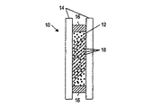
ここで図1を参照すると、本明細書の説明に基づいて作成された、露光されたポリマー分散液晶材料で形成された電気的にスイッチング可能なホログラム10の断面図が示されている。ポリマー分散液晶材料の層12は、一対の錫ドープ酸化インジウムでコーティングされたスライドガラス14とスペーサ16との間に挟まれている。ホログラム10の内部は、2本の交差するコヒーレントなレーザー光のビームで生成された干渉パターンに層12が露光された時に形成される、ブラッグ型の(Bragg)透過型回折格子18を示す。露光時間及び光の強度は、所望の回折効率及び液晶ドメインサイズによって変えることができる。液晶ドメインのサイズは、光開始剤、共開始剤、及び連鎖延長剤(又は架橋剤)の濃度を変えることによって制御することができる。ITO電極を横断する外部の電界を加えることによって回折格子が記録される際に、ネマチックダイレクタの方向が制御され得る。
【0034】
引用され本明細書の一部とされた文献Applied Physics Lettersの、図2に示す走査型電子顕微鏡写真は、36重量%の液晶を負荷したサンプルに、95mW/cm2のアルゴンイオンレーザーの488nmの光線を用いて記録された回折格子の表面の写真である。液晶ドメインのサイズは約0.2μmであり、回折格子の間隔は約0.54μmである。約20μmの厚みのこのサンプルは、光をブラッグの法則に従って回折する。
【0035】
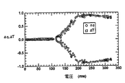
図2は、本明細書に従って作成されたホログラムの、ホログラムに加えられた電圧の二乗平均(Vrms)に対する正規化された正味の透過率及び正規化された正味の回折効率を示すグラフである。Δηは、一次ブラッグ回折効率の変化である。ΔTはゼロ次透過率の変化である。図2は、電圧を高くするにつれて、エネルギーが一次ビームからゼロ次ビームへと移っていることが示されている。約225Vrmsにおいて回折効率の真の最小値が存在する。ピーク回折効率は、プローブビームの波長及び重合に応じて、サンプルの厚みを適切に調節することにより100%に近付けることができる。最小回折効率は、硬化ポリマーの屈折率を液晶の通常屈折率と等しくさせるべくPDLC材料のパラメータを僅かに調節することによって0%に近付けることができる。
【0036】
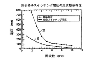
印加される電圧の周波数を高めることによって、最小回折効率に対するスイッチング電圧を著しく低下させることができる。このことは図3に示されている。図3は、二乗平均電圧の周波数に対する、最小回折効率を得るための、本明細書の説明に従って作成されたスイッチングプログラムに必要なしきい値二乗平均電圧20及び完全スイッチング二乗平均電圧22の両方を示すグラフである。しきい値及び完全スイッチング二乗平均電圧は、10kHzに於いて、それぞれ20Vrms及び60Vrmsまで下がる。より高い周波数ではより低い値となることが推定される。
【0037】
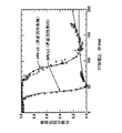
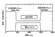
液晶ドロップレットのサイズが小さくなると、それらの方向を切り換えるためのスイッチング電圧が高くなるという問題が生ずる。前の段落で説明したように、高い周波数の交流電流スイッチング電圧を用いることが、必要なスイッチング電圧を低下させる助けとなる。図4に示すように、全混合物の約4〜6重量%の量でプレポリマー材料に界面活性剤(例えばオクタン酸)を加えると、1〜2kHzの低い周波数でスイッチング電圧が約50Vrmsのサンプルホログラムが得られる。図5に示すように、界面活性剤を用いてドロップレットのサイズを小さくすると、PDLC材料のスイッチング時間が短くなることも分かった。従って、界面活性剤を用いて作られたサンプルは、約25〜44μ秒でスイッチングすることができる。何らかの理論に結び付けることを意図しないが、界面活性剤は、液晶と硬化ポリマーとの間の界面における液晶のアンカリングを低下させることによってスイッチング電圧を低くしていると考えられる。
【0038】
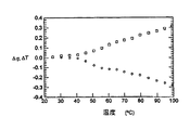
回折効率の熱的な制御が図5に示されている。図5は、本明細書の説明に従って作られたホログラムの、温度に対する正規化された正味の回折効率及び正規化された正味の透過率を示すグラフである。
【0039】
ここに開示するポリマー分散液晶材料は、そのようなポリマー分散液晶系の特定の組成の体積ホログラムを記録するために用いることができるということが立証された。
【0040】
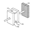
図7に示すように、PDLC反射型回折格子は、錫ドープ酸化インジウムでコーティングされたスライドガラス114a上にプレポリマー材料112の混合物の幾つかのドロップレットを置くことによって作成される。次に、第2の錫ドープ酸化インジウムでコーティングされたスライド114bを第1のスライドに押し付けて、プレポリマー材料112がスライド114aと114bとの間の領域を満たすようにする。好ましくは一様なスペーサ118を用いることによって、スライドの間隔を約20μmに維持する。プレポリマー材料の調製、スライドガラスへ移す作業は、暗所で行うのが好ましい。組立ての後、ミラー116をガラスプレート114bの裏側に設けることができる。サンプルからミラーまでの距離は、レーザーのコヒーレンス長より実質的に短いのが好ましい。PDLC材料は、好ましくは、ガラスプレートの面全体に延ばされた状態で、強度が約0.1〜100mW/cm2の488nmのアルゴンイオンレーザー光に、一般的には30〜120秒間露光される。広がったビーム内での強め合う干渉及び弱め合う干渉が、被膜の厚みを通して周期的な強度の分布を作り出す。
【0041】
或る実施態様では、反射型回折格子を作製するために用いられるプレポリマー材料が、モノマー、液晶、橋かけモノマー、共開始剤、及び光開始剤染料を含む。反射型回折格子は、ジペンタエリトリトールヒドロキシペンタクリレート(dipentaerythritol hydroxypentacrylate)(DPHA)を含むモノマーのほかに、35重量%の(E7の商品名で市販されている)シアノビフェニル(cyano biphenyls)混合物からなる液晶、10重量%のN-ビニルピロリジノン(N-vinylpyrrolidinone)("NVP")からなる架橋モノマー、25重量%の共開始剤N‐フェニルグリシン(N-phenylglycine)("NPG")、及び10−5から10−6グラムモルのローズベンガルエステル(rose bengal ester)からなる光開始剤染料を含むポリマー材料から形成され得る。更に、透過型回折格子の場合のように、界面活性剤を加えることによって、透過型回折格子に関連して上述したものと同じ有益な特性が得られると考えられる。また、プレポリマー開始材料の類似の範囲や変更についても、適切な反射型回折格子の形成に容易に適用できると考えられる。
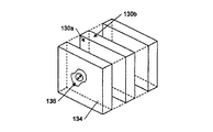
【0042】
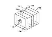
得られる材料が、表面に垂直な回折ベクトルで160nmの周期の細密な回折格子を含むことは、低電圧の高分解能走査型電子顕微鏡("LVHRSEM")によって確認された。従って、図8aに模式的に示すように、回折格子130は、前面134に平行に延在するポリマーチャネル130a及びPDLCチャネル130bの周期的な面を有する。回折格子のこれらの周期的な面に関連する間隔は、サンプルの空気−被膜界面から被膜−基板界面までの全厚みにわたって比較的一定である。
【0043】
透過型及び反射型回折格子の両方を作成するために干渉が利用されるが、反射型回折格子の形態は著しく異なっている。詳述すると、その形態は、類似の液晶濃度を有する透過型回折格子の場合と異なり、個々の液晶ドロップレットの凝集がほとんどないことが明らかであることが確認された。更に、材料に存在したドロップレットの中で直径が50〜100nmのものは非常に少なかった。更に、液晶を豊富に含む領域が、通常は回折格子の40%未満である透過型回折格子の場合と異なり、反射型回折格子の液晶を豊富に含む部分は非常に大きい。反射型回折格子の周期は非常に短い、即ち格子の間隔が非常に狭い(〜0.2μ)ことから、低い光強度の領域における硬化終了までの時間と高い強度の領域における硬化終了までの時間との差は非常に小さいと考えられる。また、ドロップレットの直径が小さくことから明らかなように、速い速度での重合によって、ゲル化の際にマトリクスにおける液晶のパーセンテージが著しく抑えられ、大きいドロップレットの成長又は小さいドロップレットのより広い領域への分散が妨げてられていると考えられる。
【0044】
吸光スペクトルに於ける反射ノッチ(反射の切れ目)の解析によって、周期的な屈折率の変化が被膜の厚み全体にわたって存在するという結論が裏付けられる。488nmのアルゴンイオンレーザーで形成されたPDLC材料において、反射ノッチは、一般的には比較的狭いバンド幅及び垂直入射光に対して約472nmの反射光波長を有する。書き込みの波長と反射の波長との間の差が僅か(約5%)であることは、被膜の収縮が、問題とならないということを示している。更に、そのような回折格子の性能は、数ヶ月間の期間にわたって安定であることが分かった。
【0045】
上述の実施例において使用された材料に加えて、適切なPDLC材料としては、トリエチレングリコールジアクリレート(triethyleneglycol diacrylate)、トリメチロール プロパントリアクリレート(trimethylolpropanetriacrylate)、ペンタエリトリトールトリアクリレート(pentaerythritol triacrylate)、ペンタエリトリトールテトラクリレート(pentaerythritol tetracrylate)、及びペンタエリトリトールペンタクリレート(pentaerythritol pentacrylate)等を挙げることができる。同様に、その他の共開始剤、例えばトリエチルアミン(triethylamine)、トリエタノールアミン(triethanolamine)、及びN, N-ジメチル-2,6-ジイソプロピルアニリン(N,N-dimethyl-2,6-diisopropylaniline)等も、N-フェニルグリシン(N-phenylglycine)の代わりに用いることができる。アルゴンイオンレーザーの458nm、476nm、488nm、514nmの波長での利用に望ましい光開始剤染料としては、ローズベンガルナトリウム塩(rose bengal sodium salt)、エオシン(eosin)、
エオシンナトリウム塩(eosin sodium salt)、フルオレセインナトリウム塩(fluorescein sodium salt)等が挙げられる。633nmの波長のレーザーの利用に際しては、メチレンブルー(methylene blue)が良く用いられる。また、その他の液晶、例えば4'-ペンチル-4-シアノビフェニル(4'-pentyl-4-cyanobiphenyl)、4'-ヘプチル-4-シアノビフェニル(4'-heptyl-4-cyanobiphenyl)等も利用可能であると考えられる。
【0046】
図8aを再度参照すると、回折格子130の前面134に平行に配置されたポリマーチャネル130a及びPDLCチャネル130bの周期的な平面を備えた本発明による反射型回折格子130の立体図が示されている。液晶ドメインの対称軸136は、回折格子130の周期的なチャネル130a及び130bに対して垂直で、且つ回折格子130の前記134に対して垂直な方向に形成される。従って、電界Eが加えられたとき、図8bに示すように、対称軸136は、既に電界Eと整合する低エネルギー状態にあり、再度配向される。従って、本発明による反射型回折格子は、通常はスイッチング可能なものとならない。
【0047】
一般に反射型回折格子は、それが反射フィルタとして用いられ得るように狭い幅の波長を反射する傾向がある。しかし、或る実施態様では、反射型回折格子がスイッチング可能となるように形成される。詳述すると、スイッチング可能な反射型回折格子が、負の誘電異方性LC(又は低いクロスオーバー周波数を有するLC)、加えられる磁界、加えられる剪断応力場、又は傾め回折格子を用いて形成され得る。
【0048】
負の誘電異方性(Δε)を有する液晶は、加えられる磁界に対して垂直な向きに旋回することが知られている。図9aに示すように、負のΔεを有する液晶で形成された液晶ドメインの対称軸136は、回折格子130の周期的なチャネル130a及び130bに対して垂直で、且つ回折格子の前面135に垂直な方向にも配向される。しかし、電界Eがそのような回折格子を横断するように加えられると、図9bに示すように、負のΔεの液晶の対称軸は歪み、回折格子の周期的な面と被膜に対して垂直な電界Eに垂直な向きに再配向される。この結果、反射型回折格子は、反射型である状態と透過型である状態との間でスイッチング可能となる。以下に示す負のΔεを有する液晶及びその他の液晶が、本発明のその方法及びデバイスにおいて用いられ得ると考えられる。
【0049】
【化2】
液晶は本来(若しくは合成された時)正又は負の何れかのΔεを有し得る。従って、低い周波数で正のΔεを有するが、高い周波数ではそれが負になるLCを用いることが可能である。Δεの符号が変わる(印加される電圧の)周波数を、クロスオーバー周波数と称する。クロスオーバー周波数は、LCの組成によって異なり、1〜10kHzの範囲の値を有するのが一般的である。従って、適切な周波数で操作することによって、反射型回折格子を切り換えることができる。正及び負の誘電異方性液晶の組合せから低いクロスオーバー周波数の材料を作成することができると考えられる。そのような組合せにおいて使用するために適した正の誘電性液晶は、以下のような四環エステルを含む。
【0051】
【化3】
そのような組合せにおいて使用するために適した強い負の誘電性液晶は、以下のようなピリダジン(pyridazine)から作られる。
【0053】
【化4】
両液晶材料は、LaRoche & Co., Switzerlandから市販されている。この組合せにおける正及び負の液晶の比率を変えることにより、室温において1.4〜2.3kHzのクロスオーバー周波数が得られる。本実施例における使用に適した他の組合せとしては、p-ペンチルフェニル-2-クロロ-4-ベンゾエート(p-ペンチルベンゾイルオキシ)ベンゾエート(p-pentylphenyl-2-chloro-4-(p-pentylbenzoyloxy)benzoate)及びベンゾエート(benzoate)が挙げられる。これらの材料は、Kodak Companyより入手可能である。
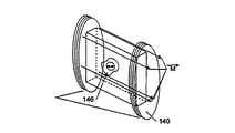
【0055】
更に詳述すると、スイッチング可能な反射型回折格子が、正のΔεの液晶を用いて形成され得る。図10aに示すように、そのような回折格子は、PDLC開始材料を硬化プロセスの間に磁界にさらすことによって形成される。この磁界は、(図10aに示すような)ヘルムホルツコイルの使用、永久磁石の使用、又は他の適切な手段の使用により生成することができる。好ましくは、磁界Mは、回折格子140を形成するために用いられる板ガラス(図示せず)の前面と平行な向きに加えられる。この結果、液晶の対称軸146は、混合物が液体である間に磁界に沿った向きに配向される。重合が終了する時に磁界が取り除かれ、液晶の対称軸と一致する向きがそのまま維持される(図10b参照)。電界が加えられると、図10cに示すように、正のΔεの液晶が電界の方向に再配向され、その方向は回折格子の前面及び回折格子の周期的なチャネルに対して垂直な向きである。
【0056】
図11aは、斜め透過型回折格子148を示し、図11bは斜め反射型回折格子150を示す。ホログラフィー透過型回折格子は、回折格子のベクトルGの方向が回折格子表面と平行でない場合に斜めになると考えられる。ホログラフィー反射型回折格子では、回折格子ベクトルGが回折格子の表面に対して垂直でない場合に斜めになると言われている。斜め回折格子は、ディスプレイ装置、ミラー、ラインフィルタ、光学スイッチ等の、斜め型でない回折格子と同一の多くの用途を有する。
【0057】
第1に、斜めホログラフィー回折格子を用いて、回折されたビームの方向を制御する。例えば、反射ホログラムにおいて、斜め回折格子を用いて、被膜の表面反射を回折ビームから分離する。PDLCホログラフィー回折格子では、斜め回折格子がより有利な点を有する。斜め型であることによって、接線方向又はホメオトロピック方向の何れかの方向に配向された液晶を用いた時に、回折格子の変調の深さを電界によって制御することが可能となる。これは、この斜め方向が、電界の成分を回折格子ベクトルに対して接線方向と垂直方向の両方向に供給するからである。詳述すると、反射型回折格子の場合、LCドメインの対称軸は、回折格子ベクトルGに沿った向きに配向され、長さ方向に加えられた電界Eによって薄膜の面に対して垂直な向きにスイッチングされ得る。これは、斜め反射型回折格子の回折効率のスイッチングのための一般的な幾何学的形態(geometry)である。
【0058】
斜め反射型回折格子に記録する時には、2つの直角のガラスプリズムの斜辺同士の間にサンプルを置くことが望ましい。次に濃度フィルタを屈折率が整合した流体を用いてプリズムの裏面に光学的に接触する形で置き、同様に記録される回折格子を生じさせる逆方向反射を生じないようにすることができる。入射レーザービームは、従来型のビームスプリッタによって2本のビームに分割され、それらのビームは次にプリズムの前面に向けられ、所望の角度でサンプルにおいて重なる。従って、これらのビームはサンプルに互いに反対側から入射することになる。このプリズムカップリング技術によって、より大きな角度で光をサンプル当てることが可能となる。得られる回折格子の傾きは、プリズムアセンブリが回される角度(即ち、1本の入射ビームの向きと、そのビームがプリズムに入射する位置におけるプリズム前面の法線との間の角度)によって決定される。
【0059】
図12に示すように、スイッチング可能な反射型回折格子は、加え得られる剪断応力場の存在の下で形成され得る。この方法では、剪断応力が、磁界Mの方向に沿って加えられる。このことは、例えば、ポリマーが柔らかい状態である間にプレポリマー混合物を間に挟んだ2枚のITOでコーティングした板ガラスに同じ大きさの反対方向の引張り力を加えることによって達成することができる。この剪断応力によって、応力の方向にLCドメインが歪み、得られるLCドメイン対称軸は主として応力の方向に沿った、PDLC平面に平行で且つスイッチングのために加えられる電界の方向に垂直な向きとなる。
【0060】
この説明に従って作成された反射型回折格子は、カラー反射型ディスプレイ、レーザー保護のためのスイッチング可能な波長フィルタ、反射型光学要素等の用途に用いることができる。
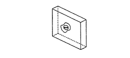
【0061】
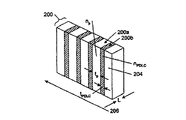
或る実施態様では、PDLC材料を複屈折として知られる特性を示すように作製することができる。複屈折によって、回折格子を透過する偏光した光が、変化した偏光を有することになる。そのような回折格子は、波長以下回折格子(subwavelength grating)として知られ、それらは方解石、リン酸カリウム、又はニオブ酸リチウム等の負の単軸結晶のような挙動を示し、光軸がPDLC面に対して垂直である。ここで図13を参照すると、回折格子200の前面204に垂直な、ポリマー面200aとPDLC面200bとが周期的に存在する面を有する、本明細書の説明に従って作製された透過型回折格子200の立体図が示されている。光軸206は、ポリマー面200a及びPDLC面200bに対して垂直な向きである。各ポリマー面200aは厚みtp及び屈折率npを有し、各PDLC面200bは厚みtPDLC及び屈折率nPDLCを有する。
【0062】
ここでPDLC平面とポリマー平面の複合的厚みは光学的波長(即ち、 (tPDLC + tP) <<λ)よりも概ね小さく、回折格子は複屈折性を示す。後述するように、偏光のシフト大きさは回折格子の長さに比例する。従って、所定の光の波長に対する波長以下回折格子の長さLを慎重に選択することによって、偏光面を回転させ或いは円偏光を生じさせることが可能である。従って、そのような波長以下回折格子を半波長若しくは4分の1波長板として機能するようにそれぞれ設計することが可能である。従って、このプロセスの利点は、その波長における与えられた任意の材料の複屈折に依存するのではなく、むしろ材料の複屈折を単純な設計パラメータによって調節して特定の波長に対して最適化し得ることである。
【0063】
半波長板を形成するためには、波長以下回折格子の遅れ(retardance)が波長の半分(即ち、遅れ=λ/2)と等しくなければならず、また4分の1波長板を形成するためには、その遅れが波長の1/4(即ち、遅れ=λ/4)に等しくなければならない。遅れは正味の複屈折|Δn|に関係し、それは次式のような波長以下回折格子の常光線屈折率noと異常光屈折率neとの差である。
遅れ = |Δn|L = |ne−no|L
従って、半波長板(即ち、遅れが波長の半分に等しい)の場合、波長以下回折格子の長さは次のように選択され得る。
L = λ/(2|Δn|)
同様に、4分の1波長板(即ち、遅れが波長の1/4に等しい)の場合、波長以下回折格子の長さは次のように選択され得る。
L = λ/(4|Δn|)
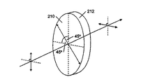
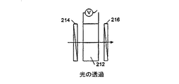
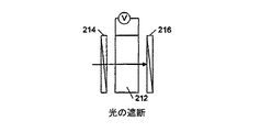
図14aに示すように、例えば入射する偏光が半波長板212の光軸210に対して45°の角度である場合、平面偏光は保存されるが板を出る波の偏光は90°シフトし得る。従って、半波長板212が組合されたポーラライザー214及び216の間に配置された図14b及び図14cに示すように、入射光が透過される。図14dに示すように適切なスイッチング電圧を印加した場合、偏光は回転せず、光は第2のポーラライザーによって遮断される。
【0064】
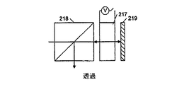
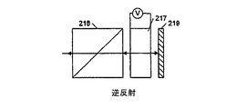
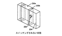
4分の1波長板の場合、偏光は円偏光に転換される。従って、4分の1波長板217がビームスプリッター218とミラー219との間に配置された図15aに示すように、反射光はビームスプリッター218によって反射される。図15bに示すように適切なスイッチング電圧が印加された場合、反射光はビームスプリッターを通過し、入射ビームに沿って逆反射される。
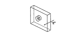
【0065】
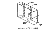
図16aには、前述の方法によって記録された、回折格子230の前面234に対して垂直に配置されたPDLCチャネル230b及びポリマーチャネル230aの周期的平面を有する波長以下回折格子230の立体図を示す。図16aに示すように、液晶ドメインの対象軸232は、回折格子の表面234に対して平行に、また回折格子230の周期的チャネル230a及び230bに対して垂直に配置される。従って、図15bに示すように回折格子に電界Eを印加すると、対称軸232は歪んで電界Eの方向に再配向され、回折格子の前面234に対して垂直に、また回折格子230の周期的チャネル230a及び230bに対して平行となる。結果として、波長以下回折格子230によって、入射する偏光を変化させる状態と変化させない状態の間で切替えが可能である。何らかの理論に結び付けられることを意図しないが、液晶ドメインの対象軸232の方向は、回折格子の記録の際のモノマー及び液晶の異方性の分散の結果生じる表面張力勾配によるもであり、またこの勾配によって液晶ドメインの対象軸が周期的平面に対して垂直に方向づけられると考えられる。
【0066】
Born and Wolf, Principles of Optics, 5th Ed., New York (1975)(ここで言及することにより本明細書の一部とする)に開示のように、波長以下回折格子の複屈折は次式によって与えられる。
【0067】
【数1】
ここで、
no=波長以下回折格子の常光線屈折率
ne=異常光屈折率
nPDLC=PDLC平面の屈折率
np=ポリマー平面の屈折率
nLC=入射光で見られる液晶の有効屈折率
fPDLC= tPDLC/(tPDLC+tp)
fp= tp/(tPDLC+tp)
従って、nPDLC = npの場合、波長以下回折格子の複屈折はゼロである。
【0069】
液晶の有効屈折率nLCは、電界の幾つかの値において電界がゼロでポリマーの値npと等しい値であるときに最大値EMAXをとる印加された電界の関数であることが知られている。従って電界の印加によって、液晶の屈折率nLCが変更され、よってPDLC平面の屈折率が変更され得る。前述の関係を用いれば、波長以下回折格子の正味の複屈折は、nPDLCがnpに等しいとき(即ち、nLC= np)最小となる。従って、電界を印加することによってPDLC平面の屈折率がポリマー平面の屈折率に一致する場合(即ち、nPDLC= np)、波長以下回折格子の複屈折が消え得る。
【0070】
Born及びWolf(前出)の式から、正味の複屈折(即ち、|Δn|=|ne−no|)に対する式は以下のようになる。
【0071】
【数2】
ここで、nAVG=(ne+no)/2
更に、次式で示すように、PDLC平面の屈折率nPDLCは、入射光で見られる液晶の有効屈折率nLC及び周囲のポリマー平面の屈折率nPと関係する。
NPDLC= nP+fLC[nLC−nP]
ここで、fLCはPDLC平面におけるポリマーに分散した液晶の体積分率であり、fLC=[VLC/(VLC+VP)]である。
【0073】
例えば、電界のない場合の液晶の有効屈折率の標準的な値は、nLC=1.7であり、またポリマー層に対してはnP=1.5である。PDLC平面とポリマー平面の厚みとが等しく(即ち、tPDLC= tP、fPDLC= 0.5 = fP)且つfLC=0.35である回折格子の場合、波長以下回折格子の正味の複屈折Δnは約0.008である。従って、入射光が0.8μmの波長を有する場合、波長以下回折格子の波長は、半波長板に対して50μmであり、4分の1波長板に対して25μmとなる。更に、約5V/μmの電界を印加することによって、液晶の屈折率がポリマーの屈折率と一致し、半波長の回折格子の複屈折が消え得る。従って、半波長板に対するスイッチング電圧Vnは約250Vであり、4分の1波長板に対するスイッチング電圧は約125ボルトである。
【0074】
そのような電圧を印加することによって、板はマイクロ秒のオーダーでオン状態とオフ状態(ゼロ遅れ)の間でスイッチングされ得る。比較の手段として、電流ポッケルスセル技術は約1000−2000Vの電圧でナノ秒でスイッチングされ、またバルクネマチック液晶は約5Vの電圧でミリ秒のオーダーでスイッチングされ得る。
【0075】
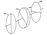
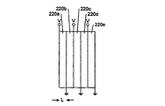
図17に示すような別の実施例において、波長以下回折格子のスイッチング電圧は、波長以下回折格子220a−220eを共に積み重ね、それらを電気的に並列に連結することによって低減することができる。例えば、各々が10μmの長さを有する5つの回折格子の積み重ねが、半波長板に必要とされる厚みを生じさせることが知られている。各回折格子は、透明な電極として機能する錫ドープ酸化インジウムコーティングを含むので、サンプルの長さは、50μmよりも幾分大きいことに注意されたい。しかしながら、そのような板の積み重ねに対するスイッチング電圧は単に50Vに過ぎない。
【0076】
前述の波長以下回折格子は、電気通信、測色法、分光分析、レーザ保護などのためのチューナブルフィルタだけでなく、ディスプレイ及びレーザ光学素子のための偏光子及び光学スイッチの分野において適切な用途が見出されることが期待される。同様に、電気的にスイッチング可能な透過型回折格子は、光線が偏向されたり、或いはホログラフィー像が切換えられるような多くの用途を有する。このような用途には、光ファイバースイッチ、光学的結合のためのリプログラマブルNxN光学的相互接続、レーザメスのためのビームステアリング、レーザレーダーのためのビームステアリング、ホログラフィーイメージの記録及び検索、デジタルズーム光学要素(スイッチング可能なホログラフィーレンズ)、グラフィック技術及びエンターテイメントなどが含まれる。
【0077】
スイッチング可能なホログラムでは、電場の印加によってホログラムの回折効率が変更され、完全なオン状態(高い回折効率)から完全なオフ状態(低い回折効率若しくは0)へと切換え可能である。静的ホログラムでは、その特性は印加された電場に依存せず固定されたままである。本発明によれば、ハイコントラストな状態のホログラムが生成可能である。変更例において、ホログラムは前述のように記録される。次に硬化したポリマーフィルムを短時間室温にて適切な溶媒に浸漬し、最終的に乾燥させる。液晶E7の場合、メタノールが十分な適応性を示す。可能性のある他の溶媒としては、メタノールのようなアルコール、ヘキサン及びヘプタンのような炭化水素などが挙げられる。材料を乾燥すると、高い回折効率を有するハイコントラストな状態のホログラムが生じる。第2の層ドメインは空の間隙(空気)(n〜1)に置き換えられるので、高い回折効率はフィルム(Δn〜0.5)における大きな屈折率変調(index modulation)の結果である。
【0078】
同様に本発明によれば、高い複屈折の静的な波長以下波長板(subwavelength wave-plate)を形成可能である。空気の屈折率は殆どの液晶の屈折率に比べて十分低いため、対応する半波長板の厚みが低減され得る。本発明により合成された波長板は、特にコストが高すぎるため若しくは嵩張るために適切な波長が適切な複屈折の材料に利用できない偏光子を用いる多くの用途において使用可能である。
【0079】
用語「ポリマー分散液晶」及び「ポリマー分散液晶材料」には、モノマーが重合若しくは硬化していない溶液、ある程度の重合が生じている溶液、並びに完全に重合した溶液が含まれる。当業者は、当業者が標準的に用いる用語であるポリマー分散液晶(文法的には完全に重合した基質に分散された液晶を指す)が、より文法的に正しいポリマー分散液晶材料若しくは文法的により正しいポリマー分散液晶材料の出発原料の一部又はその全てを含むことを意味することを理解するであろう。
【0080】
図18:スイッチング可能なホログラフィー光学要素
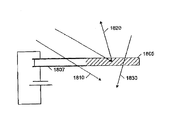
図18は、動作しているスイッチング可能なホログラフィー光学要素(HOE)の一実施形態を示す。本図において、電場はスイッチング可能なHOE1805の一部を横断し、電極板1807を通過して印加される。電場はHOEから回折格子構造を有効に消去することによってHOEを透過する。電極板1807のうち電場にさらされていないスイッチング可能なHOE1805の部分は、図中で斜線により示されている回折格子構造がそのままの状態で残っているために、なおもホログラムとして機能する。好適な入射角で入射する好適な色の光線1820は、HOE1805の前記部分により回折される。しかし、電極板1807間のスイッチング可能なHOE1805の前記部分に入射する光線1810は、スイッチング可能なHOE1805を通過して伝搬される。また、光がスイッチング可能なHOE1805の帯域外にあるか、光線がHOEと交差する領域において入射角がスイッチング可能なHOE1805の回折角と近似していないかのいずれかの場合には、光線1830のような光もスイッチング可能なHOE1805の回折部分を通過して伝搬される。1807等の多数の電極板を用いて、スイッチング可能なHOE1805の適切な箇所に好適な電場を印加することにより、スイッチング可能なHOE1805の多数の異なる部分で回折、部分回折、または透過を起こさせることが可能である。印加電場を調整すれば、回折光の強度はダイナミックレンジで制御可能である。より具体的には、印加電場が変化すると回折効率がそれに伴い変化する。電場が増大すると修正屈折率が小さくなり、ゆえにゼロ次方向(例えば、入射光線方向)から回折光線方向への透過光が減少し、結果として回折効率も低下する。電場が縮小して修正屈折率が大きくなれば、結果的にゼロ次方向から回折光線方向により多くの光が透過する。一実施形態において、HOEは薄型格子ホログラムである。他の実施形態では、スイッチング可能なHOE1805は、ブラッグ型ホログラムまたは高回折効率の体積ホログラムである。
【0081】
スイッチング可能なHOE1805を用いた本システム一実施形態は、高屈折効率及び高スイッチング速度で特徴づけられるホログラムが記録可能なフォトポリマー/液晶複合材料から構成される。スイッチング可能なHOE1805は透過電極間に挟持され、電極により印加された電場を調節することにより回折態から不動態へスイッチすることが可能である。
【0082】
スイッチング可能なHOE1805は、例えば図1に示す材料のような露出PDLC材料を含む。PDLC材料は露出プロセス(例えばホログラム記録プロセス)中に相分離を行い、液晶ドロップレット(小滴)によって稠密にされ、クリアフォトポリマー領域によって散布される領域を作る。電場は露出PDLCに印加され、液晶ドロップレットの固有配向を変化させる。前記液晶ドロップレットは逆に干渉縞の修正屈折率を小さくし、ホログラムの回折効率を極小レベルに低下させ、そこに記録されたホログラムを効率的に消去する。回折態では、電場は印加されず、露出PDLC材料は極めて高い回折効率を示す。露出PDLC材料は回折態と実質上の透過態との間を急速にスイッチする(例えば、露出材料は数十マイクロセカンドでスイッチ可能であり、これは通常の液晶ディスプレイ材料と比べて非常に速い)。
【0083】
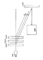
図19−図20:光源とホログラフィー光学要素との結合
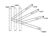
図19は、異なる色の光源を組み合わせて多色光を発生させるシステムの一実施形態を示す。本システムでは、3つの色が異なる光の発生源、赤色光源1910R、緑色光源1910G、及び青色光源1910Bからの光が、3つのHOE1920R、1920G、及び1920Bから構成されるHOEスタック(stack)に入射する。各HOEは単色の回折光に形成される。HOE1920Rは赤色光を回折し、HOE1920Gは緑色光を回折し、HOE1920Bは青色光を回折する。3つの光源各々からの光は3つのHOEのうち対応する1つのHOEによって共通の出射方向へ回折され、対応する感色性を有しないHOEを通過して実質的に伝搬される。HOE1920R、1920G、及び1920Bは、各HOEからの回折光が実質的に重なり合うように配列する。出射光は混合光1930Wのビームとして進行する。好適な実施形態では、出射光1930Wが実質的に「白」光となるように3つの光源の相対強度及び3つのHOEの回折効率を一致させる。
【0084】
本システムの一実施形態において、HOE1920R、1920G、及び1920Bは、スイッチング可能なホログラムではない。前記HOEは、回折効率及び角感度を予め決定した固定(fixed)回折構造を有する。他の実施形態では、3つのHOEのうち少なくとも1つのHOEは、スイッチング可能なHOEである。前記スイッチング可能なHOEを横断する印加電場を制御することにより、回折効率は変動する。個々の色成分が回折効率の変動性を有することで出射光1930Wの色彩のバランスがとれる。この変動性によって、3つの光源1910R、1910G、及び1910Bの明るさの変化を打ち消すことが可能である。例えば、いくつかの実施形態では、赤色光のより大きな成分を有する白色光源が好適である。HOE1920Rに電場を印加して回折効率を向上させると、結果として出射光1930Wは目的のようにさらに赤くなる。別法では、通常運転中に3つの光源1910R、1910G、及び1910Bの全てを最大強度で動作させ、1910G及び1910Bの強度を低下させて出射光1930Wを赤くすることも可能である。
【0085】
より簡易なシステムでは含まれるHOEも少ない。例えば、2つの単色光源を組み合わせるシステムは、ミラーの前に反射型HOEを配置して作製する。本システムにおいて、HOEは1色を出射方向に回折させるように配置・配列する。HOEの格子は第1の色に特に反応するので、第2の色の光は実質的に変化することなくHOEを通過する。第2の色はミラーからはね返って、HOEを通過して出射方向に反射する。
【0086】
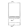
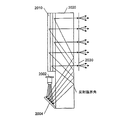
図20a及び図20bは、ホログラフィー照明システムの他の実施形態を示す。システムは一連のLED2002、ミラー2004、ライトガイド2020、反射HOEスタック2010、及びディフューザ2030を含む。ライトガイド2020は、HOEスタック2010を反射光で照明するように配置する。HOEスタック2010のHOEは、光をコリメートし、例えばビームスプリッターを用いて反射ディスプレイ面に組み合わせできる位置から光をディフューザ2030に向ける。図20a及び図20bに示した例では、HOEスタック2010はライトガイド2020の裏面に取設されている。本実施形態では、ライトガイド2020は裏面からLED2002からの3色の光を受け、前面からの光をHOEスタック2010へ反射する。この反射は全内部反射とすることが可能であり、あるいはライトガイド2020の前面の一部を銀めっき(silvering)または部分銀めっきして反射させることも可能である。既述の実施形態では、HOEスタック2010は3つの反射型HOEを含み、各HOEは3色のうち1色の光を回折するように配置する。各HOEの干渉縞の幾何学的配置(geometry)(例えば、修正屈折率)は、回折光が実質的にコリメートな光線経路でHOEの各部から現れるようにする。従って、回折光は有効にコリメートする。HOEスタック2010からの回折光は、ライトガイド2020を通過してディフューザ2030に再び伝播され、ディフューザ2030はライトガイド2020の前面に装着または隣接させる。他の実施形態では、ライトガイド2020を設計する際に適宜異なる光線経路の幾何学的配置が用いられる。
【0087】
LED2002は、好適には狭い帯域に集中する高出力の明るい光源である。HOEスタック2010は、異なるLEDから実質的に一様な白光までの光の異なる色成分と組み合わせ、前記白光をディフューザ2030へ伝搬するよう配置する。個々のLEDは、LEDの光がHOEスタック2010に好適な入射角で入射するよう配列する。
【0088】
他の実施形態では、レーザーダイオード、ハロゲンランプ、誘導ランプ、アークランプ等を単独もしくは組み合わせて用い、LED2002に替わる照明源とすることが可能である。照明源は単色光または広帯域とすることが可能である。また、HOEスタック2010は、反射HOE要素に代えて伝搬可能なHOE要素で構成することが可能である。要素を替えた実施形態の一例を図21に示す。
【0089】
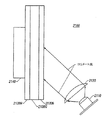
図21:透過 HOE を有する照明システム
ホログラフィック光学要素を用いる照明システム2100の別の実施例が図21aに示されている。照明システムは、光源2110と、コリメートレンズ2120と、反射型のイメージディスプレイ2140を照らすのに用いられる透過HOEスタック2130とを有する。HOEスタック2130及びディスプレイ2140の組み合わせは、例えば、限定空間での映像投射装置に用いられうる。
【0090】
ある実施例に於いて、スタック2130は少なくとも3つの透過型スイッチング可能HOEを有する。HOE2130R−2130Bの各々は、そこへ供給される電圧に応じて活動状態と非活動状態との間で個々にスイッチング可能であり得る。本実施例に於いて、各HOEは、光透過層及び電導層に挟まれたポリマー分散型液晶マテリアル層と、光透過層及び非電導層に挟まれたものの組み合わせとを含む。あるいは、HOEはグループとして活動状態と非活動状態との間でスイッチング可能である。本実施例に於いて、HOE2130R−2130Gは、光透過層及び電導層に挟まれた3つのそれぞれ別個のポリマー分散型液晶マテリアル層と、光透過層及び非電導層に挟まれたものの組み合わせとを含みうる。HOE2130R−2130Gに関するより詳細な記述に関しては、US Patent Application 09/478,150のOptical Filter Employing Holographic Optical Elements and Image Generating System Incorporating The Optical Filter(January 5,2000)、US Patent Application 09/533,120のMethod And Apparatus For Illuminating A Display(March 23,2000)、及びUS Patent Application 09/675,431のInspection Device(September 29,2000)を引用することをもって本明細書の一部とする。別の実施例に於いては、HOEスタック2130はスイッチング不可能なHOEを有しうる。
【0091】
本実施例に於いて、光源2110は、概ね、白熱ランプ、インダクションランプ、蛍光灯、若しくはアークランプ、その他のランプのような、広帯域白色光源である。別の実施例に於いては、光源2110は、赤、緑、青の異なる色の単色光の組であり得る。それらの光源はLED、レーザーダイオード、若しくはその他の単色光源でありうる。
【0092】
ディスプレイ2140は、HOE2130を挟んで光源2110と反対側面に配置されている。ディスプレイ2140は一つあるいは複数の実施例の形態をとりうる。映像ディスプレイは、スクリーンの各リフレッシュの間におけるピクセル強度状態を調整するアクティブTFTコントロール物質を有したシリコン上の反射型マイクロLCDのような、反射型マイクロディスプレイの形態をとりうる。映像ディスプレイは、光反射型マイクロ、若しくはピクセル強度を制御するミニチュア反射要素の再配置するMEMS装置の形態をとりうる。典型的なマイクロミラー装置は、Texas InstrumentsよりDigital Light Processorの名称で市販されている。映像ディスプレイは、回折装置の出現範囲の一つの形態もとりうる。典型的なそのような装置の一つは、Silicon Light Machines,Incより、Grating Light Valveの名称で市販されている。その他の実施例では、ディスプレイ2140は透過ディスプレイであり、照明システムの光学的装置は、反射型HOEの複数のスタック間に配置された偏光回転体を有するスイッチング可能な透過性HOEの二つのスタックを含むように構成されうる。
【0093】
システム2100に於いて、HOEスタック2130は、映像ディスプレイの前面に直接配置される。光源2110より発せられる照明光は、レンズ2120によりコリメートされ、適切な入射角度でHOEスタック2130に照射される。コリメートされた照明光の一つもしくは複数の要素は、HOEスタック2130の一つ若しくは複数のHOEにより、続いてディスプレイ2140に向かって回折させられる。上記の通り、HOEスタックは、透過性のHOEを有している。透過性HOEが、照明光のs−偏光成分をほとんど変更することなく透過させるに対して、活動状態では照明光のp−偏光成分を回折させるべく形成される。代わりに、照明光のp−偏光成分をほとんど変更することなく透過させるに対して、活動状態では照明光のs−偏光成分を回折させるべく形成されるような透過性のHOEを採用することは可能であり得る。本発明は、照明光のs−偏光をほとんど変更することなく透過させ、p−偏光を回折させる透過型HOEに関して詳述しうる。「変更することなく」というのは、回折することなく、強度を変更することなく、位相を変化させることなくと言う意味で定義されるが、以上に制限されるものではない。
【0094】
図21b−図21dは図21aに示された照明システム2100の動作を図示している。図21b及び21cは、反射型マイクロLCDとして既述の、ディスプレイ2140が反射型マイクロディスプレイの形態をとるときの照明システム2100を示している。図21dは、ディスプレイ2140が反射型マイクロミラーの形態をとるときの照明システム2100を示している。図21b−図21dのディスプレイ2140は、入射する照明光を反射また変調してイメージ光を生成する。この照明光はディスプレイ2140へ供給されるイメージ情報に応じて変調される。別の記載では、照明光は、記録されたイメージを伴いディスプレイ2140によって反射される。図21b及び図21cのマイクロディスプレイは照明入射光の偏光を回転させ、図21dのそれは回転させない。
【0095】
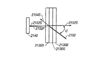
図21b−21dは、HOEスタック2130を示す。HOEスタック2130は個々にスイッチング可能な透過型HOEである2130R−2130Bを有し、それらは、活動状態において、コリメートされた照明光のs−偏光された赤、緑、及び青の幅の成分を透過し、コリメートされた照明光のp−偏光された赤、緑、及び青の幅の成分をそれぞれ回折する。非活動状態ではスタック2130におけるそれぞれのHOEは、変更を伴う事なく概ねすべてのコリメートされた光を透過する。HOE2130R−2130Bのいずれかによって第一次回折光へと回折させられるp−偏光の割合は、既述の電導層及び光透過層間の電圧の強度に依存する。それ故、HOE2130R−2130Bの電圧の強度を調整することにより、前記システムは、光源2110から得る照明光のカラーバランスを保つ手段を得る。HOE2130R−2130Bの3つのすべてのHOEは、同時、もしくは連続的または周期的に活動状態であり得る。最近の実施例ではHOE2130R−2130Bのそれぞれが連鎖的に一つずつ活性化され、ディスプレイ2140は表示させたい画像の青、緑、赤の要素を通して周期的に変化させる。HOEスタック2130は、ディスプレイ2140上の画像を伴い、人間の目が色を統合する時間(integration time)(100マイクロ秒以下)よりも短時間で周期的にスイッチングされる。この方式ではシステムはカラーのイメージを供給するためにシングルモノクロマチックディスプレイを用いる。
【0096】
図21b−21dは、アクティブ状態で操作されるHOE2130R及び、非活動状態で操作されるHOE2130Gおよび2130Bを示す。図21bでは、s−偏光赤帯域幅成分2152Sがほとんど変更されることなく透過されているのにたいして、平行照明光2150のp−偏光赤帯域幅成分2152PがHOE2130Rにより回折させられている。回折光2152Pはディスプレイ2140により、s−偏光赤帯域幅イメージ光2152Sとして反射され、すなわち偏光方向を回転させられる。イメージ光2152Sがs−偏光であるため、イメージ光2152Sは、2130R−2130BのすべてのHOEを完全もしくは概ね変更されることなく透過する。HOEスタック2130を透過するイメージ光2152Sは、観賞用のスタンダードプロジェクター光学素子(図示されない)により投影される。HOEのポリマー分散液晶層、及びまたは、HOEスタック2130によりイメージ光がレシーブされる角度U範囲内の回折格子は、イメージ及び照明光2152S及び2152Pが、ディスプレイ装置2140及びHOE2130R−2130Bの表面にノーマルであるように配置されうる。2154Sを含む回折を伴わない照明光2150の残存成分は、ディスプレイ2140によって反射される場合、イメージ光2152Sとは異なる角度で浮かび上がる。このゼロオーダー光(非回折光)が異なった出現角度を有しているため、それがイメージ光2152Sと干渉しないように捉えられ、若しくは、そのような傾向を有しうる。既述のとおり、アクティブなHOEにより回折させられるp−偏光照明光の割合は、そこでの電圧強度に依存する。それはまた、HOEが照明光を受ける角度Uにも依存する。角度Uが50度から60度の間もしくはそれ以下の場合、概ねすべてのp―偏光成分照明光が回折される。しかし、HOEにより回折されるp−偏光照明光の割合は、角度Uが50度から60度を超えて増えるにつれて、概ね減少しうる。
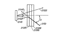
【0097】
図21cは概ね図21bに準ずる。しかし21aとは異なり、回折されたp−偏光照明光2152pが、ディスプレイ表面の通常軸に対して非ゼロ角でディスプレイ2140に入射する。反射されたs−偏光イメージ光2154sも、ディスプレイ2140よりディスプレイ表面の通常軸に関して角度を有して浮かび上がる。しかしながらイメージ光2152sはs−偏光であり、HOEスタック2130を、完全に若しくは概ね変更されることなく透過する。2154Sを含む回折を伴わない照明光2150の残存成分は、ディスプレイ2140によって反射される場合、イメージ光2152Sの出現角度よりも大きな角度で浮かび上がる。このゼロオーダー光(即ち、回折されない光)が、より大きな出現角度を有している為、それがイメージ光2152Sと干渉しないように捉えられ、若しくは、そのような傾向を有しうる。
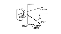
【0098】
図21dは図21cに準ずる。しかし既述の通りディスプレイ装置2140がイメージ入射光の偏光を回転させない。つまり、p−偏光イメージ光2156Pはディスプレイ2140から浮かび上がる。しかし、p−偏光イメージ光2156Pとp−偏光イメージ光2152Pとの間の角度Vが、HOE2130R−2130Bのブラッグ回折角帯域幅よりも大きい場合、イメージ光2156Pは、HOE2130R−2130Bを完全若しくは概ね変化することなく透過する。
【0099】
図22:色分け及び色の釣り合わせ
図22は、白色光をそれぞれの色成分に分ける装置を示す。この装置は、2210R、2210G及び2210Bの3つのHOE要素で構成され、それらのそれぞれが、赤色、緑色及び青色の光に回折可能である。HOEは、多色性或いは幅の広い光源2205からの光によって照明される。そぞれのHOEは、光源2205からの色成分の1つをディスプレイ2220に向かうように回折する。次に、2220から反射された光が投影装置2230に入射する。
【0100】
HOE要素210R、2210G及び2210Bは、スイッチング可能なHOEである。これらが1個ずつ順次オンとなるため、ディスプレイ2220は、順次、青、緑、赤に照明される。ディスプレイユニット2220はまた、目的の画像の3原色の内の1つを順次表示するようにスイッチングされる。HOE2210R、2210G及び2210Bは、ディスプレイ2220のスイッチングと同期してスイッチングされるが、その速度は肉眼による画像の形成より速い。従って、投影される画像は、1つの単色ディスプレイ2220によって形成される複合カラーの画像である。
【0101】
赤色、緑色、青色(人間の目における錐状体の3つのタイプの基準となる色の幅(nominal color band))に調整されたHOEを用いる代わりに、目的に応じて他の色を組合わせることも可能であることに注目されたい。一般に、好適な色の幅をもつ色成分の任意のセットを利用できる。例えば、緑がかった青色(cyan)、黄色、紫紅色(magenta)の組み合わせが、ある種の印刷に用いられる。
【0102】
上記した実施例におけるスイッチング可能なHOEは、高い回折効率を実現するためにブラッグ型の要素を用いることが可能である。しかしながら、ブラッグ型HOEと比べると回折効率は高くないが、薄い相のスイッチング可能なHOEを用いることも可能である。更に、光学装置の変更に合わせて反射型スイッチング可能HOEを透過型スイッチング可能HOEに換えることができ、またはその逆も可能である。同様に、透過型非スイッチ式HOEを反射型非スイッチ式HOEに換えることができ、またその逆も可能である。
【0103】
上記した実施例において、HOE及びその他の光学要素によって発生する光学収差を補償するために、従来の光学要素が必要となる場合がある。これらの補償要素は、この装置の基本的な機能の記載に影響を与えるものではないため、単純化するべくこれらの要素を省略した。光学収差を補償するために、こららの装置の或る実施例にHOEを使用する場合もあり得ることに注意されたい。
【図面の簡単な説明】
【図1】 露出ポリマー分散液晶(PLDC)材料により構成され電気的にスイッチング可能なホログラムの断面図。
【図2】 界面活性剤を付加することなく構成されたホログラムの正規化された正味透過率及び正規化された正味回折効率を、ホログラムに加えられたrms電圧に対して示したグラフ。
【図3】 ホログラムを切り替えるのに必要な閾値及び完全スイッチングrms電圧を示す、最小回折効率対rms電圧周波数グラフ。
【図4】 界面活性剤が存在した状態の34重量%の液晶を用いたPLDC材料及び29%の液晶並びに4重量%の界面活性剤を用いたPLDC材料についての、加えられた電界の関数としての正規化された回折効率のグラフ。
【図5】 図4の界面活性剤を含むPLDC材料について、回折ビームのスイッチング応答時間特性を示すグラフ。
【図6】 ホログラムの正規化された正味透過率及び正規化された正味回折効率を示すグラフ。
【図7】 反射型回折格子を記録するための実験のための典型的構成を示す立体図。
【図8A】 前面に対して平行なポリマーチャネル及びPLDCチャネルの周期的面を有する反射型回折格子の、電界が加えられない状態を示す立体図であって、回折格子の構成に用いられた液晶が正の誘電異方性を有する。
【図8B】 前面に対して平行なポリマーチャネル及びPLDCチャネルの周期的面を有する反射型回折格子の、電界が加えられた状態を示す立体図であって、回折格子の構成に用いられた液晶が正の誘電異方性を有する。
【図9A】 格子の前面に対して平行なポリマーチャネル及びPLDCチャネルの周期的面を有する反射型回折格子の、電界が加えられない状態を示す立体図であって、回折格子の構成に用いられた液晶が負の誘電異方性を有する。
【図9B】 格子の前面に対して平行なポリマーチャネル及びPLDCチャネルの周期的面を有する反射型回折格子の、電界が加えられた状態を示す立体図であって、回折格子の構成に用いられた液晶が負の誘電異方性を有する。
【図10A】 ヘルムホルツコイル内に配置された反射型回折格子の立体図。
【図10B】 電界が加えられない状態の図10aに示された反射型回折格子の立体図。
【図10C】 電界が加えられた状態の図10aに示された反射型回折格子の立体図。
【図11A】 ポリマーチャネル及びPLDCチャネルの周期的面の格子ベクトルGの方向を示す斜めの透過型回折格子の側面図。
【図11B】 ポリマーチャネル及びPLDCチャネルの周期的面の格子ベクトルGの方向を示す斜めの反射型回折格子の側面図。
【図12】 剪断応力場が加えられた状態の反射型回折格子の立体図。
【図13】 回折格子の前面に対して直交するように配置されたポリマーチャネル及びPLDCチャネルの周期的面を有する波長以下回折格子の立体図。
【図14A】 入射光の偏光方向が90度回転するような半波長板として機能する、本発明に基づき構成された波長以下回折格子の立体図。
【図14B】 入射光を透過させるように、互いに交差する偏光子間に配置された、図14aに示されたスイッチング可能な半波長板の立体図。
【図14C】 半波長板に電圧を加えて入射光の偏光方向が回転しないようにして、第2の偏光子により入射光をブロックするようにした、図14bに示されたスイッチング可能な半波長板及び互いに交差する偏光子を示す側面図。
【図14D】 半波長板に電圧を加えて入射光の偏光方向が回転しないようにして、第2の偏光子により入射光をブロックするようにした、図14bに示されたスイッチング可能な半波長板及び互いに交差する偏光子を示す側面図。
【図15A】 波長以下回折格子が4分の1波長板として機能し、平面偏光された光が、波長以下回折格子を透過し、ミラーにより逆反射され、ビームスプリッターにより反射されるようにした波長以下回折格子の側面図。
【図15B】 図15aに示されたスイッチング可能な4分の1波長板を示す側面図であって、4分の1波長板に電圧を加えることにより、光の偏光状態が変化しないようにし、反射された光がビームスプリッターを通過するようにしたことを示す。
【図16A】 回折格子の前面に対して直交するように配置されたポリマーチャネル及びPLDCチャネルの周期的面を有し、電界が加えられない状態の透過型回折格子の立体図であって、回折格子の構成に用いられた液晶が正の誘電異方性を有する。
【図16B】 回折格子の前面に対して直交するように配置されたポリマーチャネル及びPLDCチャネルの周期的面を有し、電界が加えられた状態の透過型回折格子の立体図であって、回折格子の構成に用いられた液晶が正の誘電異方性を有する。
【図17】 回折格子が積み重ねられ、かつ電気的に並列接続され、波長以下回折格子の切り替え電圧が低くなるようにした、波長以下回折格子の側面図。
【図18】 選択的に透過型とされ得るスイッチング可能な光学要素の図。
【図19】 異なるカラーの光を結合させるのに積重ねた光学的要素を用いるシステムの一実施例を示す図。
【図20a】 異なるカラーの光を結合させるのに積重ねた光学的要素を用いるシステムの別の実施例を示す図。
【図20b】 異なるカラーの光を結合させるのに積重ねた光学的要素を用いるシステムの別の実施例を示す図。
【図21a】 イメージディスプレイを照明するのに積重ねた透過型のホログラフィー光学的要素を用いるシステムの一実施例を示す図。
【図21b】 図21aに示すシステムの一実施例の操作的態様を示す図。
【図21c】 図21aに示すシステムの一実施例の操作的態様を示す図。
【図21d】 図21aに示すシステムの別の実施例の操作的態様を示す図。
【図22】 カラーシーケンスイメージディスプレイに対して照明源におけるカラー強度をバランスさせるために透過型のスイッチング可能なホログラフィー光学素子の積重ねが用いられるシステムの一実施例を示す図。[0001]
(Technical field)
The present invention relates to illumination systems, and in particular to illumination systems that use one or more switchable holographic optical elements for illumination of image displays.
[0002]
(Background art)
Image displays are used in projection display systems. Projection display systems are a growing technology in the television and digital monitor markets. The projection display provides an image to the user using an image concentrated on the diffuser. Projection can be done from the diffuser on the same side as the user, as in the projector, or from the opposite side. In general, an image is generated on one or more “displays” (small LCD devices that reflect or transmit light in a pattern formed by switchable pixels). LCD displays are usually manufactured by microelectronic processing technology. Each pixel in the display is an area whose reflection or transmission characteristics can be controlled by an electrical signal. In an LCD display, light incident on a specific pixel is reflected, partially reflected, or blocked by the pixel according to a signal given to the pixel. In some cases, the LCD display is a transmissive device, and the transmission through any pixel changes step by step (gray level) from the state where light is largely blocked to the state where incident light is generally transmitted. obtain. Recently, displays have been made up of micro electromechanical devices (MEMs) that incorporate a small movable mirror. One or more of its mirrors in each pixel adjusts whether light is reflected in the output direction.
[0003]
When a uniform light beam is reflected from the display or transmitted through the display, the light beam obtains a specific intensity profile that depends on the transmission state of the pixel. In order to correspond to the requested image, the image is generated on the LCD by adjusting the transmission (or gray level) of the pixels. This image is projected onto a diffusing screen for direct view, or onto several intermediary image surfaces, where they are magnified by an eyepiece to produce a virtual image, such as in a wearable display. Can give.
[0004]
The display is typically a monochrome device and each pixel is in an “on” or “off” state, or set to an intermediate intensity level. A display usually cannot individually control the intensity of one or more color components of an image. To perform color control, the display system can use three independent LCD displays. Each of the three LCD displays is illuminated by a separate light source having a spectral component that stimulates one of the three types of cones in the human eye. Each of the three displays reflects (or transmits) light rays that produce one color component of the color image. The three rays are then combined by a prism, dichroic filter and / or other optical element into a monochromatic image beam.
[0005]
Another method of generating a full color image that eliminates the problem of combining light beams from three separate displays illuminates a single monochrome display that is updated with the appropriate primary color components of the image. .
[0006]
The display is formed as an array of red, green and blue pixels, which is illuminated by white light with an array of color filters used to illuminate each pixel having the appropriate color. However, color image generation in this way can reduce image resolution since only one of the three pixels is available for each primary color.
[0007]
An important part of the design considerations for these systems includes the selection of a light source and means for effectively controlling the relative intensity of the light source. This control requires that effective color balancing is possible during initial calibration and operation.
[0008]
In essence, the hologram produces a waveform that is predetermined by the diffractive structure recorded on the holographic media. Holograms can be used to reproduce the action of certain optical elements such as lenses or mirrors. In some cases, “holographic optical elements” (HOE) are based on simple diffraction gratings, and complex optical operations may not be reproduced. These HOEs are simpler and less expensive to construct than glass equivalents, especially when the optical elements are complex or when strict tolerances must be met.
[0009]
HOE is compact and lightweight, and its wavelength characteristics improve its adaptability in the design of optical systems. HOE can be used to replace individual optical elements, groups of optical elements, and in some cases, conventional optical elements throughout the system.
[0010]
(Disclosure of the invention)
An apparatus and method for illuminating an image display with an electrically switchable holographic optical element is disclosed. The method includes the step of a first electrically switchable holographic optical element (ESHOE) receiving illumination light. The first ESHOE includes opposing front and back surfaces. The first ESHOE diffracts the first component of illumination light (eg, p-polarized blue light) while transmitting the remaining component of the illumination light substantially unchanged. An image display is prepared and receives the diffracted first component. In response to receiving the diffracted first component, the image display emits image light. The first ESHOE receives the image light and transmits it almost unchanged. In one embodiment, the diffracted first component emerges from the back of the first ESHOE and the image light is in a direction generally parallel to the diffracted first component emerging from the back of the first ESHOE. As received by the first ESHOE, the first ESHOE receives image light on its back side.
(BEST MODE FOR CARRYING OUT THE INVENTION)
While the invention is susceptible to various modifications and alternative forms, specific embodiments have been shown by way of example in the drawings and will be described in detail below. However, the drawings and detailed description thereof are not intended to limit the present invention, and all modifications, changes and modifications may be made without departing from the scope and spirit of the invention as defined by the appended claims. It should be understood to include equivalents and alternatives.
[0011]
Several types of illumination systems can be constructed with holographic optical elements (HOE). These systems can be used to combine light sources of different colors to provide polychromatic or “white” light illumination. A switchable (or “reconfigurable”) HOE allows the intensity adjustment of the individual color components of white light. A switchable HOE can also be used in a system that produces a color image by color sequence illumination of a monochrome image display (or “video display”).
[0012]
1-17: Switchable hologram materials and devices
The present invention provides, in one embodiment, a holographic optical element formed from a polymer dispersed liquid crystal (PDLC) material comprising a monomer, a dispersed liquid crystal, a crosslinking monomer, a coinitiator, and a photoinitiator dye. Is used. These PDLC materials exhibit a clear and orderly separation of the liquid crystal and the cured polymer, thereby providing the advantage that the PDLC material becomes a high quality optical element. PDLC materials used in holographic optical elements can be formed in a single step. The holographic optical element uses a unique photopolymerizable prepolymer material that allows in-situ control over the properties of the resulting diffraction grating, such as domain size, shape, density, position ordering, etc. You can also. Further, the methods and materials disclosed herein can be used to make PDLC materials for optical elements that include switchable transmissive or reflective holographic diffraction gratings.
[0013]
Polymer dispersed liquid crystal materials, methods and devices used in the present invention are described in RL Sutherland et al. Bragg Gratings in an Acrylate Polymer Consisting of Periodic Polymer dispersed Liquid-Crystal Planes, Chemisrry of Materials, No. 5, pp. 1533-1531 (1993). RL; Sutherland et al. "Electrically switchable volume gratings in polymer dispersed liquid crystals," Applied Physics Letters, Vol. 64, No. 9, pp. 1074-1076 (1994); and TJ Bunning et al. "The Morphology and Performance of Holographic Transmission Gratings Recorded in Polymer dispersed Liquid Crystals, "Polymer, Vol. 36, No. 14, pp. 2699-2701 (1995), etc., all of which are incorporated herein by reference. To do. U.S. Patent Application Nos. 08 / 273,436 and 5,698,343 entitled "Switebable Volume Hologram Materials and Devices," and "Laser Wavelength Detection and Energy Dosimetry Badge," by Sutherland et al. Are also incorporated herein by reference. In these patent specifications, background materials used for forming a transmissive diffraction grating in a volume hologram are disclosed.
[0014]
The process by which holograms for use in embodiments of the present invention are formed is largely controlled by the choice of components used to prepare a uniform starting mixture and, to a lesser extent, the intensity of the incident light pattern. It is also controlled by. Certain types of polymer dispersed liquid crystal (PDLC) materials used in the present invention produce a switchable hologram in a single step. One type of PDLC material is characterized by patterned anisotropic diffusion (or reverse diffusion) of polymerizable monomers and second phase materials, especially liquid crystals (LC), upon irradiation with a non-uniform and coherent light pattern. ) Is started. Thus, well-defined channels of material enriched in alternating phases can be created in a single process separated by well-defined channels of substantially pure polymer.
[0015]
The resulting PDLC material may have anisotropically dispersed, phase-separated LC droplets within a photochemically cured polymer matrix. Conventional PDLC materials created by a one-step process could only obtain large LC bubble regions and smaller LC bubble regions in the polymer matrix. Large bubble sizes are highly dispersed, producing a blurred appearance and multiple orders of diffraction. In contrast, small LC bubbles of certain PDLC materials in well-defined channels of LC-rich materials allow well-defined first and zero order diffraction. In PDLC materials, theoretically alternating, well-defined LC-rich channels and nearly pure polymer channels are possible by a multi-step process, but in such processes, certain types of PDLC There is no morphological control with high accuracy on the LC-rich channels and polymer width and size distributions and LC droplet sizes enabled by the material.
[0016]
The same can be made by coating the mixture between two tin-doped indium oxide (ITO) coated glass slides separated by a spacer, usually having a thickness of 10-20 μm. Place the sample in a conventional holographic recording setup. The diffraction grating usually has an intensity of about 0.1 to 100 mW / cm.2In general, recording is performed with an exposure time of 30 to 120 seconds by using a 488 nm argon ion laser. By changing the angle of the two beams and changing the interval between the intensity peaks, the interval between the diffraction gratings of the resulting hologram is changed. Photopolymerization is induced by a pattern of light intensity. A more detailed description of an example recording device can be found in RL Sutherland et al. "Switchable holograms in new phoropolymer-liquid crystal composite materials," Society of Photo-Optical Instrumentation Engineers (SPIE), Proceedings Reprint, Volume 2402, reprinted from Diffractive and Holographic Optics Technology II (1995), which is hereby incorporated by reference.
[0017]
The characteristics of the PDLC material are greatly influenced by the components used in the preparation of a uniform starting mixture, and to a lesser extent by the intensity of the incident light pattern. In some embodiments, the prepolymer material comprises a photopolymerizable monomer, a second phase material, a photoinitiator dye, a coinitiator, a chain extender (or crosslinker), and Has a surfactant as desired.
[0018]
In one embodiment, the two main components of the prepolymer mixture are a polymerizable monomer and a second phase material, preferably fully blended. Highly functionalized monomers are preferred. This is because such monomers shrink to some extent to form a densely crosslinked network that tends to be extruded from the second phase material. As a result, the second phase material is anisotropically detached from the polymer region and segregates into a well-defined low polymer region and a second phase rich region or domain. Highly functionalized monomers may also be preferred. The high degree of cross-linking associated with such monomers causes fast kinetics and allows the hologram to be formed relatively quickly, so that the second phase material is present in domains of size less than about 0.1 μm. Because it becomes.
[0019]
However, highly functionalized monomers are relatively viscous. As a result, these monomers are difficult to mix with other materials and difficult to extend into a thin film. Accordingly, it is preferred to use a mixture of penta-acrylates in combination with di-, tri-, and / or tetra-acrylates to optimize both functionalization and viscosity of the polymeric material. Suitable acrylates such as triethyleneglycol diacrylate, trimethylolpropane triacrylate, pentaerythritol triacrylate, pentaerythritol tetra-acrylate, pentaerythritol pentaacrylate (Pentaerythritol penta-acrylate) and the like can be used. In some embodiments, an approximately 1: 4 mixture of triacrylate and pentaacrylate promotes uniform mixing and provides a mixture suitable for forming a 10-20 μm film on an optical plate. I understood.
[0020]
The selected second phase material is liquid crystal (LC). This also allows an electro-optical response to the resulting hologram. The concentration of LC used should be high enough to allow sufficient phase separation to occur in the cured sample, but so high that the sample is impervious or very blurry. Should not be concentration. If it is less than about 20% by weight, almost no phase separation occurs and the diffraction efficiency becomes low. If it exceeds about 35% by weight, the degree of dispersion of the sample increases, and both the diffraction efficiency and the transmittance decrease. Samples made generally at a concentration of about 25% by weight provide good diffraction efficiency and optical clarity. In a prepolymer mixture using a surfactant, the concentration of LC can be increased to 35 wt% without compromising optical performance by adjusting the amount of surfactant. Suitable liquid crystals for use in the practice of the present invention include cyanobiphenyls mixture, 4′-n-pentyl-4-cyanobiphenyl (4′-n-pentyl), commercially available from Merck under the product name E7. -4-cyanobiphenyl), 4'-n-heptyl-4-cyanobiphenyl (4'-n-heptyl-4-cyanobiphenyl), 4'-octaoxy-4-cyanobiphenyl, Examples thereof include 4′-pentyl-4-cyanoterphenyl and α-methoxybenzylidene-4′-butylaniline. Other second phase components can also be used.
[0021]
The polymer dispersed liquid crystal material used in the practice of the present invention is dipentaerythritol hydroxypentacrylate (available from, for example, Polysciences, Inc. Warrington, Pennsylvania), commercially available under the product name E7 from Merck. 10-40 wt.% Liquid crystal E7 (available from BDH Chemicals, Ltd, London, England), chain extension (available from Aldrich Chemical Company, Milwaukee, Wisconsin) Monomer N-vinylpyrrolidinone ("NVP"), co-initiator N-phenylglycine ("NPG") (available from Aldrich Chemical Company, Milwaukee, Wisconsin) (Commercially available from Spectragraph, Ltd Maumee, Ohio under the product name RBAX) and rose benga ester, a photoinitiator dye l ester)
[0022]
The mixture of liquid crystal and prepolymer material is homogenized by suitable means (for example, ultracentrifugation) to form a solution having viscosity, and usually tin-doped oxidation using a spacer having a thickness of 15 to 100 μm, preferably 10 to 20 μm. Extend between glass slides coated with indium (ITO). ITO is conductive and serves as an optically transmissive electrode. The prepolymer material preparation, mixing, and transferring to a glass slide are preferably performed in a dark place because the photosensitivity of the mixture is very high.
[0023]
The sensitivity of the prepolymer material to light intensity depends on the photoinitiator dye and its concentration. Photosensitivity increases when the concentration of the dye is high. In many cases, however, the solubility of the photoinitiator dye will limit the concentration of the dye, which in turn limits the sensitivity of the prepolymer material. However, in many normal applications, in order to achieve the desired sensitivity and to fully bleach the dye in the recording process to obtain a final uncolored sample, 0.2-0. A photoinitiator dye concentration in the range of 4% by weight has been found to be sufficient. Photoinitiator dyes that can be used to produce PDLC materials include rose bengal esters (2, 4, 5, 7-tetraiodo-3 ', 4', 5 ', 6'-tetrachlorofluorescence- 6-acetate ester); rose bengal sodium salt; eosin; eosin sodium salt; 4,5-diiodosuccinylfluorescein; camphorquinone; methylene blue and the like. These dyes provide sensitivity to recording wavelengths over the visible light spectrum of nominally 400-700 nm. It has also been found that suitable near infrared dyes, for example, cationic cyanine dyes containing trialkylyl borate anions that absorb light at 600 to 900 nm, merocyanine dyes derived from spiropyran, etc. can be used in the present invention .
[0024]
The coinitiator used in the practice of the present invention controls the cure rate in the free radical polymerization reaction of the prepolymer material. The optimum phase separation and the optimum diffraction efficiency in the resulting PDLC material is a function of the cure rate. It has been found that favorable results can be achieved by using coinitiators in the range of 2-3% by weight. Suitable coinitiators include N-phenylglycine; triethylamine; triethanolamine; N, N-dimethyl-2,6-diisopropylaniline and the like.
[0025]
Other suitable dye and coinitiator combinations suitable for the practice of the invention, particularly in the visible light region, include eosin and triethanolamine; camphorquinone and N-phenylglycine (N-phenylglycine); fluorescein and triethanolamine; methylene blue and triethanolamine or N-phenylglycine; erythrosin B and triethanol Examples thereof include amines (triethanolamine); indolinocarbocyanine and triphenyl borate; indobenzospiropyran and triethylamine.
[0026]
Chain extenders (or crosslinkers) used in the practice of the present invention can help increase the rate of polymerization as well as increase the solubility of the components of the prepolymer material. The chain extender is preferably a small vinyl monomer as compared to pentaacrylate, and by using a small vinyl monomer, the pentaacrylate monomer cannot be easily accessed due to steric hindrance. It becomes easy to react with the position of the acrylate in the acrylate monomer. Accordingly, the reaction between the chain extender monomer and the polymer increases the propagation length of the growing polymer. In normal applications, it has been found that a chain extender in the range of 10-18% by weight maximizes performance in terms of diffraction efficiency. In certain embodiments, suitable chain extenders are N-vinylpyrrolidinone, N-vinyl pyridine,
Selected from the group consisting of acrylonitrile, N-vinyl carbazole and the like.
[0027]
It has been found that adding a surfactant material, i.e. octanoic acid, to the prepolymer material can lower the switching voltage and increase the diffraction efficiency. Specifically, the switching voltage of PDLC materials containing surfactants is significantly lower than the switching voltage of PDLC materials made without surfactants. Although not intended to be tied to a specific theory, these results are thought to be due to the weak anchoring force between the polymer and the phase separated LC droplets. SEM studies have shown that the size of the droplets in PDLC materials containing surfactants is reduced to 30-50 nm and the dispersion is more uniform. In such materials, the proportion of smaller droplets increases, which reduces random scattering and increases diffraction efficiency. Therefore, the shape of the droplet is closer to a sphere than when the surfactant is present, thereby lowering the switching voltage.
[0028]
In more general applications, it has been found that samples containing only 5% by weight of surfactant have significantly lower switching voltages. Also, when optimizing for low switching voltages, the surfactant concentration can vary up to about 10% by weight (often determined by the LC concentration), which greatly increases the diffraction efficiency. It has been found that the switching voltage increases with a lower (possibly due to a reduction in the total phase separation of the LC). Suitable surfactants include octanoic acid; heptanoic acid; dodecanoic acid and the like.
[0029]
In the sample using octanoic acid as the surfactant, it was estimated that the free carboxyl group (COOH) in octanoic acid was present, but it was observed that the conductivity of the sample increased. As a result, the sample rises in temperature when an electric field of high frequency (˜2 KHz) is applied for a long time. Therefore, it is desirable to add a surfactant to reduce high conductivity without sacrificing high diffraction efficiency and low switching voltage. A suitable electrically switchable diffraction grating is vinyl neononanoate ("VN") C, a polymerizable monomer commercially available from Aldrich Chemical Co. in Milwaukee, Wisconsin.8H17CO2CH = CH2It was found that can be formed from Favorable results were also obtained when the chain extender N-vinylpyrrolidinone ("NVP") and the surfactant octanoic acid were replaced with 6.5 wt% VN. VN also acts as a chain extender due to the presence of reactive acrylate monomer groups. In these changes, a sample with high optical quality having a diffraction efficiency of about 70% was obtained, and the resulting diffraction grating could be electrically switched by applying an electric field of 6 V / μm.
[0030]
The PDLC material used in the present invention may be formed using a liquid crystal bifunctional acrylate (“LC monomer”) as a monomer. LC monomers are highly miscible with low molecular weight nematic LC materials, promote the formation of high concentrations of low molecular weight LCs, and create samples with high optical quality, making conventional acrylate monomers Better than. When low molecular weight LC is present at high concentration in PDLC materials, the switching voltage is reduced (eg to ˜2 V / μm). Another advantage of using an LC monomer is that in a LC droplet, a weak AC or DC electric field is applied during hologram recording to prealign the host LC monomer and low molecular weight LC. The desired direction and configuration of the nematic director can be obtained. The chemical formulas for some suitable LC monomers are as follows:
[0031]
[Chemical 1]
Semifluorinated polymers are known to exhibit weaker anchoring properties and a significantly lower switching field. Accordingly, it is considered that a semi-fluorinated acrylate monomer that is a bifunctional liquid crystal is suitable for use in the present invention.
[0033]
Referring now to FIG. 1, there is shown a cross-sectional view of an electrically
[0034]
The scanning electron micrograph shown in FIG. 2 of the document Applied Physics Letters, cited and incorporated herein, is 95 mW / cm on a sample loaded with 36 wt% liquid crystal.22 is a photograph of the surface of a diffraction grating recorded using a 488 nm beam of an argon ion laser. The size of the liquid crystal domain is about 0.2 μm, and the distance between the diffraction gratings is about 0.54 μm. This sample, about 20 μm thick, diffracts light according to Bragg's law.
[0035]
FIG. 2 is a graph showing normalized net transmission and normalized net diffraction efficiency versus the root mean square (Vrms) of the voltage applied to the hologram for a hologram made in accordance with the present specification. Δη is a change in the first-order Bragg diffraction efficiency. ΔT is a change in the zero-order transmittance. FIG. 2 shows that as the voltage is increased, energy is transferred from the primary beam to the zero-order beam. There is a true minimum of diffraction efficiency at about 225 Vrms. The peak diffraction efficiency can approach 100% by appropriately adjusting the thickness of the sample depending on the wavelength of the probe beam and the polymerization. The minimum diffraction efficiency can approach 0% by slightly adjusting the parameters of the PDLC material to make the refractive index of the cured polymer equal to the normal refractive index of the liquid crystal.
[0036]
By increasing the frequency of the applied voltage, the switching voltage for the minimum diffraction efficiency can be significantly reduced. This is illustrated in FIG. FIG. 3 shows both the threshold mean
[0037]
When the size of the liquid crystal droplet is reduced, there arises a problem that the switching voltage for switching the direction becomes high. As explained in the previous paragraph, using a high frequency alternating current switching voltage helps reduce the required switching voltage. As shown in FIG. 4, when a surfactant (eg, octanoic acid) is added to the prepolymer material in an amount of about 4-6% by weight of the total mixture, a sample hologram with a switching voltage of about 50 Vrms at a low frequency of 1-2 kHz Is obtained. As shown in FIG. 5, it was also found that when the droplet size was reduced using a surfactant, the switching time of the PDLC material was shortened. Thus, a sample made with a surfactant can switch in about 25-44 microseconds. Without intending to be bound by any theory, it is believed that surfactants lower the switching voltage by reducing the anchoring of the liquid crystal at the interface between the liquid crystal and the cured polymer.
[0038]
The thermal control of diffraction efficiency is shown in FIG. FIG. 5 is a graph showing normalized net diffraction efficiency and normalized net transmittance versus temperature for a hologram made in accordance with the description herein.
[0039]
It has been demonstrated that the polymer-dispersed liquid crystal materials disclosed herein can be used to record volume holograms of a specific composition of such polymer-dispersed liquid crystal systems.
[0040]
As shown in FIG. 7, a PDLC reflective diffraction grating is created by placing several droplets of a mixture of
[0041]
In some embodiments, the prepolymer material used to make the reflective grating comprises a monomer, a liquid crystal, a crosslinking monomer, a coinitiator, and a photoinitiator dye. In addition to monomers containing dipentaerythritol hydroxypentacrylate (DPHA), the reflective diffraction grating is made from a 35% by weight (commercially available under the E7 trade name) mixture of cyano biphenyls. A liquid crystal, 10% by weight of a crosslinking monomer consisting of N-vinylpyrrolidinone ("NVP"), 25% by weight of a co-initiator N-phenylglycine ("NPG"), and 10-5To 10-6It can be formed from a polymeric material containing a photoinitiator dye consisting of gram moles of rose bengal ester. Furthermore, it is believed that the same beneficial properties as described above in connection with the transmissive diffraction grating can be obtained by adding a surfactant, as in the case of the transmissive diffraction grating. Also, similar ranges and modifications of the prepolymer starting material can be easily applied to the formation of an appropriate reflective diffraction grating.
[0042]
It was confirmed by a low voltage high resolution scanning electron microscope ("LVHRSEM") that the resulting material contained a fine diffraction grating with a diffraction vector perpendicular to the surface and a period of 160 nm. Thus, as schematically shown in FIG. 8a, the
[0043]
Although interference is used to create both transmissive and reflective diffraction gratings, the shape of the reflective diffraction grating is significantly different. More specifically, it was confirmed that the form is clear that there is almost no aggregation of individual liquid crystal droplets, unlike the case of a transmission type diffraction grating having a similar liquid crystal concentration. Furthermore, very few droplets having a diameter of 50 to 100 nm were present in the material. Furthermore, unlike the case of a transmissive diffraction grating in which the region rich in liquid crystal is usually less than 40% of the diffraction grating, the portion of the reflective diffraction grating rich in liquid crystal is very large. The period of the reflective diffraction grating is very short, that is, the interval between the gratings is very narrow (˜0.2 μ). The difference is considered to be very small. Also, as is evident from the small diameter of the droplets, the polymerization at a fast rate significantly reduces the percentage of liquid crystal in the matrix during gelation, which leads to large droplet growth or larger areas of small droplets. It is thought that the dispersion to
[0044]
Analysis of reflective notches in the absorption spectrum supports the conclusion that periodic refractive index changes exist throughout the coating thickness. In PDLC materials formed with a 488 nm argon ion laser, the reflective notch typically has a relatively narrow bandwidth and a reflected light wavelength of about 472 nm for normal incident light. A small difference (approximately 5%) between the writing wavelength and the reflecting wavelength indicates that the shrinkage of the coating is not a problem. Furthermore, the performance of such a diffraction grating has been found to be stable over a period of several months.
[0045]
In addition to the materials used in the above examples, suitable PDLC materials include triethyleneglycol diacrylate, trimethylolpropanetriacrylate, pentaerythritol triacrylate, pentaerythritol Examples thereof include tetraerythritol pentracrylate and pentaerythritol pentacrylate. Similarly, other coinitiators such as triethylamine, triethanolamine, and N, N-dimethyl-2,6-diisopropylaniline N-phenylglycine can be used instead of N-phenylglycine. Desirable photoinitiator dyes for use with argon ion lasers at wavelengths of 458 nm, 476 nm, 488 nm, and 514 nm include rose bengal sodium salt, eosin,
Examples include eosin sodium salt and fluorescein sodium salt. When using a laser with a wavelength of 633 nm, methylene blue is often used. Other liquid crystals such as 4'-pentyl-4-cyanobiphenyl and 4'-heptyl-4-cyanobiphenyl can also be used. It is thought that.
[0046]
Referring again to FIG. 8a, a three-dimensional view of a
[0047]
In general, a reflective diffraction grating tends to reflect a narrow wavelength so that it can be used as a reflective filter. However, in some embodiments, the reflective diffraction grating is formed to be switchable. Specifically, a switchable reflective grating is formed using a negative dielectric anisotropy LC (or LC with a low crossover frequency), an applied magnetic field, an applied shear stress field, or a tilted grating. Can be done.
[0048]
It is known that liquid crystals having negative dielectric anisotropy (Δε) rotate in a direction perpendicular to the applied magnetic field. As shown in FIG. 9a, the
[0049]
[Chemical 2]
Liquid crystals can have a Δε that is either positive or negative (or when synthesized). Thus, it is possible to use an LC that has a positive Δε at low frequencies, but negative at high frequencies. A frequency at which the sign of Δε changes (applied voltage) is referred to as a crossover frequency. The crossover frequency varies depending on the LC composition, and generally has a value in the range of 1 to 10 kHz. Therefore, the reflective diffraction grating can be switched by operating at an appropriate frequency. It is believed that low crossover frequency materials can be made from a combination of positive and negative dielectric anisotropic liquid crystals. Positive dielectric liquid crystals suitable for use in such combinations include tetracyclic esters as follows:
[0051]
[Chemical Formula 3]
Strong negative dielectric liquid crystals suitable for use in such combinations are made from pyridazine as follows.
[0053]
[Formula 4]
Both liquid crystal materials are commercially available from LaRoche & Co., Switzerland. By changing the ratio of the positive and negative liquid crystals in this combination, a crossover frequency of 1.4 to 2.3 kHz is obtained at room temperature. Other combinations suitable for use in this example include p-pentylphenyl-2-chloro-4-benzoate (p-pentylphenyl-2-chloro-4- (p-pentylbenzoyloxy)) benzoate) and benzoate. These materials are available from the Kodak Company.
[0055]
More specifically, a switchable reflective diffraction grating can be formed using a positive Δε liquid crystal. As shown in FIG. 10a, such a diffraction grating is formed by exposing the PDLC starting material to a magnetic field during the curing process. This magnetic field can be generated by the use of Helmholtz coils (as shown in FIG. 10a), the use of permanent magnets, or other suitable means. Preferably, the magnetic field M is applied in a direction parallel to the front surface of the glass sheet (not shown) used to form the
[0056]
FIG. 11 a shows an oblique transmission
[0057]
First, an oblique holographic diffraction grating is used to control the direction of the diffracted beam. For example, in a reflection hologram, an oblique diffraction grating is used to separate the surface reflection of the coating from the diffracted beam. In PDLC holographic diffraction gratings, oblique diffraction gratings have more advantages. By using the oblique type, the modulation depth of the diffraction grating can be controlled by an electric field when using a liquid crystal oriented in either the tangential direction or the homeotropic direction. This is because this oblique direction supplies the electric field component in both the tangential direction and the perpendicular direction with respect to the diffraction grating vector. More specifically, in the case of a reflective diffraction grating, the symmetry axis of the LC domain is oriented in a direction along the diffraction grating vector G, and in a direction perpendicular to the plane of the thin film by an electric field E applied in the length direction. Can be switched. This is a common geometry for switching the diffraction efficiency of an oblique reflection diffraction grating.
[0058]
When recording on an oblique reflection type diffraction grating, it is desirable to place a sample between the oblique sides of two perpendicular glass prisms. The density filter can then be placed in optical contact with the back surface of the prism using a fluid with matched refractive index to avoid back reflections that also produce a diffraction grating that is recorded. The incident laser beam is split into two beams by a conventional beam splitter, which are then directed to the front surface of the prism and overlap the sample at the desired angle. Therefore, these beams are incident on the sample from opposite sides. This prism coupling technique makes it possible to sample light at a larger angle. The resulting grating tilt is determined by the angle at which the prism assembly is turned (ie, the angle between the direction of one incident beam and the normal of the prism front at the position where the beam is incident on the prism). The
[0059]
As shown in FIG. 12, a switchable reflective diffraction grating can be formed in the presence of an applied shear stress field. In this method, shear stress is applied along the direction of the magnetic field M. This can be accomplished, for example, by applying the same amount of opposite tensile forces to two ITO coated sheet glasses with the prepolymer mixture in between while the polymer is in a soft state. This shear stress distorts the LC domain in the direction of the stress and the resulting LC domain symmetry axis is oriented along the direction of the stress, parallel to the PDLC plane and perpendicular to the direction of the electric field applied for switching. .
[0060]
Reflective diffraction gratings made in accordance with this description can be used in applications such as color reflective displays, switchable wavelength filters for laser protection, reflective optical elements, and the like.
[0061]
In some embodiments, PDLC materials can be made to exhibit a property known as birefringence. Due to birefringence, the polarized light transmitted through the diffraction grating will have a changed polarization. Such diffraction gratings are known as subwavelength gratings, which behave like negative uniaxial crystals such as calcite, potassium phosphate, or lithium niobate, with the optical axis at the PDLC surface. Is perpendicular to. Referring now to FIG. 13, a
[0062]
Where the combined thickness of the PDLC plane and the polymer plane is the optical wavelength (ie (tPDLC + tP) Generally smaller than << λ) and the diffraction grating exhibits birefringence. As will be described later, the magnitude of the polarization shift is proportional to the length of the diffraction grating. Therefore, it is possible to rotate the polarization plane or generate circularly polarized light by carefully selecting the length L of the diffraction grating below the wavelength for a given light wavelength. Therefore, it is possible to design such sub-wavelength diffraction gratings to function as half-wave or quarter-wave plates, respectively. Thus, the benefits of this process do not depend on the birefringence of any given material at that wavelength, but rather the birefringence of the material can be adjusted by simple design parameters to be optimized for a particular wavelength. That is.
[0063]
In order to form a half-wave plate, the retardation of the sub-wavelength grating must be equal to half the wavelength (ie, lag = λ / 2) and to form a quarter-wave plate The delay must be equal to 1/4 of the wavelength (ie, delay = λ / 4). The delay is related to the net birefringence | Δn |, which is the ordinary refractive index n of the subwavelength diffraction grating asoAnd extraordinary refractive index neIs the difference.
Delay = | Δn | L = | ne−no| L
Thus, for a half-wave plate (ie, the delay is equal to half the wavelength), the length of the sub-wavelength grating can be selected as follows.
L = λ / (2 | Δn |)
Similarly, for a quarter wave plate (ie, the delay is equal to 1/4 of the wavelength), the length of the subwavelength grating can be selected as follows.
L = λ / (4 | Δn |)
As shown in FIG. 14a, for example, if the incident polarization is at a 45 ° angle with respect to the
[0064]
In the case of a quarter wave plate, the polarized light is converted to circularly polarized light. Accordingly, the reflected light is reflected by the
[0065]
FIG. 16a shows a three-dimensional view of a sub-wavelength diffraction grating 230 having a periodic plane of
[0066]
As disclosed in Born and Wolf, Principles of Optics, 5th Ed., New York (1975) (which is hereby incorporated by reference), the birefringence of a subwavelength grating is given by Given.
[0067]
[Expression 1]
here,
no= Ordinary ray refractive index of diffraction grating below wavelength
ne= Extraordinary refractive index
nPDLC= PDLC plane refractive index
np= Refractive index of polymer plane
nLC= Effective refractive index of liquid crystal seen by incident light
fPDLC= tPDLC/ (TPDLC+ tp)
fp= tp/ (TPDLC+ tp)
Therefore, nPDLC = npIn this case, the birefringence of the diffraction grating below the wavelength is zero.
[0069]
Effective refractive index n of liquid crystalLCIs the value n of the polymer with zero electric field at several values of the electric field.pMaximum value E when equal toMAXIs known to be a function of the applied electric field. Therefore, by applying an electric field, the refractive index n of the liquid crystalLCCan be changed, and thus the refractive index of the PDLC plane can be changed. Using the above relationship, the net birefringence of the sub-wavelength diffraction grating is nPDLCIs np(Ie, nLC= np) Minimal. Thus, by applying an electric field, the refractive index of the PDLC plane matches the refractive index of the polymer plane (ie, nPDLC= np), The birefringence of the diffraction grating below the wavelength can disappear.
[0070]
From the equation of Born and Wolf (above), the net birefringence (ie, | Δn | = | ne−noThe formula for |) is:
[0071]
[Expression 2]
Where nAVG= (ne+ No) / 2
Furthermore, as shown by the following equation, the refractive index n of the PDLC planePDLCIs the effective refractive index n of the liquid crystal seen in the incident lightLCAnd the refractive index n of the surrounding polymer planePRelated to.
NPDLC= nP+ fLC[nLC−nP]
Where fLCIs the volume fraction of the liquid crystal dispersed in the polymer in the PDLC plane, fLC= [VLC/ (VLC+ VP)].
[0073]
For example, the standard value of the effective refractive index of a liquid crystal without an electric field is nLC= 1.7 and n for the polymer layerP= 1.5. PDLC plane and polymer plane thickness are equal (ie tPDLC= tP, FPDLC= 0.5 = fP) And fLCFor a diffraction grating where == 0.35, the net birefringence Δn of the subwavelength diffraction grating is about 0.008. Accordingly, when the incident light has a wavelength of 0.8 μm, the wavelength of the sub-wavelength diffraction grating is 50 μm for the half-wave plate and 25 μm for the quarter-wave plate. Furthermore, by applying an electric field of about 5 V / μm, the refractive index of the liquid crystal matches the refractive index of the polymer, and the birefringence of the half-wavelength diffraction grating can disappear. Therefore, the switching voltage V for the half-wave platenIs about 250V and the switching voltage for a quarter wave plate is about 125 volts.
[0074]
By applying such a voltage, the plate can be switched between an on state and an off state (zero lag) on the order of microseconds. As a means of comparison, current Pockels cell technology can be switched in nanoseconds at a voltage of about 1000-2000V, and bulk nematic liquid crystals can be switched in the order of milliseconds at a voltage of about 5V.
[0075]
In another embodiment, such as shown in FIG. 17, the switching voltage of subwavelength gratings can be reduced by stacking
[0076]
The aforementioned subwavelength diffraction gratings are suitable for use in the field of polarizers and optical switches for displays and laser optics as well as tunable filters for telecommunications, colorimetry, spectroscopic analysis, laser protection, etc. Is expected to be found. Similarly, electrically switchable transmissive diffraction gratings have many uses where light rays are deflected or holographic images are switched. Such applications include fiber optic switches, reprogrammable NxN optical interconnects for optical coupling, beam steering for laser scalpels, beam steering for laser radar, holographic image recording and retrieval, digital zoom optical elements ( Switchable holographic lens), graphic technology and entertainment.
[0077]
In a switchable hologram, the diffraction efficiency of the hologram is changed by the application of an electric field, and can be switched from a completely on state (high diffraction efficiency) to a completely off state (low diffraction efficiency or 0). In static holograms, the properties remain fixed independent of the applied electric field. According to the present invention, a hologram in a high contrast state can be generated. In the modified example, the hologram is recorded as described above. The cured polymer film is then dipped in a suitable solvent for a short time at room temperature and finally dried. In the case of liquid crystal E7, methanol shows sufficient adaptability. Other possible solvents include alcohols such as methanol, hydrocarbons such as hexane and heptane. Drying the material produces a high contrast hologram with high diffraction efficiency. Since the second layer domain is replaced by an empty gap (air) (n˜1), the high diffraction efficiency is the result of a large index modulation in the film (Δn˜0.5).
[0078]
Similarly, according to the present invention, a high birefringence subwavelength wave-plate can be formed. Since the refractive index of air is sufficiently lower than that of most liquid crystals, the thickness of the corresponding half-wave plate can be reduced. Wave plates synthesized according to the present invention can be used in many applications, particularly with polarizers where the appropriate wavelength is not available for the appropriate birefringent material because it is too costly or bulky.
[0079]
The terms “polymer-dispersed liquid crystal” and “polymer-dispersed liquid crystal material” include solutions in which the monomer is not polymerized or cured, solutions in which some polymerization has occurred, and solutions that are completely polymerized. Those skilled in the art will recognize that polymer-dispersed liquid crystal (a grammatically termed liquid crystal dispersed in a fully polymerized substrate) is a term more commonly used by those skilled in the art, It will be understood that it is meant to include some or all of the starting materials for the correct polymer dispersed liquid crystal material.
[0080]
Figure 18: Switchable holographic optical element
FIG. 18 illustrates one embodiment of a switchable holographic optical element (HOE) in operation. In this figure, the electric field traverses a portion of the
[0081]
One embodiment of the present system using a
[0082]
The
[0083]
19-20: Coupling of light source and holographic optical element
FIG. 19 illustrates one embodiment of a system that combines light sources of different colors to generate multicolor light. In this system, light from three different color light sources, a red light source 1910R, a
[0084]
In one embodiment of the system,
[0085]
A simpler system also contains less HOE. For example, a system that combines two monochromatic light sources is made by placing a reflective HOE in front of a mirror. In this system, the HOE is arranged and arranged to diffract one color in the emission direction. The HOE grating is particularly responsive to the first color, so that the second color light passes through the HOE without substantially changing. The second color bounces off the mirror and passes through the HOE and reflects in the exit direction.
[0086]
Figures 20a and 20b show another embodiment of a holographic illumination system. The system includes a series of
[0087]
The
[0088]
In other embodiments, laser diodes, halogen lamps, induction lamps, arc lamps, or the like can be used alone or in combination to provide an illumination source in place of
[0089]
Figure 21: Transmission HOE Lighting system with
Another embodiment of an
[0090]
In certain embodiments, the stack 2130 has at least three transmissive switchable HOEs. Each of the
[0091]
In this embodiment, the
[0092]
The
[0093]
In the
[0094]
FIGS. 21b-21d illustrate the operation of the
[0095]
Figures 21b-21d show the HOE stack 2130. The HOE stack 2130 has 2130R-2130B, which are individually switchable transmissive HOEs, which, in the active state, have s-polarized red, green and blue width components of the collimated illumination light. Each of the p-polarized red, green, and blue width components of the transmitted and collimated illumination light is diffracted. In the inactive state, each HOE in the stack 2130 transmits substantially all of the collimated light without modification. The proportion of p-polarized light that is diffracted into the first-order diffracted light by any of the
[0096]
21b-
[0097]
FIG. 21c generally corresponds to FIG. 21b. However, unlike 21a, the diffracted p-polarized illumination light 2152p is incident on the
[0098]
FIG. 21d corresponds to FIG. 21c. However, as described above, the
[0099]
Figure 22: Color coding and color balancing
FIG. 22 shows an apparatus for dividing white light into respective color components. This device is composed of three
[0100]
HOE
[0101]
Instead of using HOE tuned to red, green, blue (nominal color band of the three types of cones in the human eye), other colors are combined according to purpose Note that it is also possible. In general, any set of color components with suitable color widths can be utilized. For example, a combination of greenish blue, yellow, magenta is used for certain types of printing.
[0102]
The switchable HOE in the embodiment described above can use a Bragg type element to achieve high diffraction efficiency. However, although the diffraction efficiency is not high as compared with the Bragg type HOE, it is also possible to use a thin phase switchable HOE. Furthermore, the reflective switchable HOE can be replaced with a transmissive switchable HOE as the optical device changes, or vice versa. Similarly, a transmissive non-switched HOE can be replaced with a reflective non-switched HOE and vice versa.
[0103]
In the embodiments described above, conventional optical elements may be required to compensate for optical aberrations caused by HOE and other optical elements. Since these compensation elements do not affect the description of the basic function of this device, they have been omitted for the sake of simplicity. It should be noted that HOE may be used in certain embodiments of these devices to compensate for optical aberrations.
[Brief description of the drawings]
FIG. 1 is a cross-sectional view of an electrically switchable hologram made of an exposed polymer dispersed liquid crystal (PLDC) material.
FIG. 2 is a graph showing the normalized net transmittance and normalized net diffraction efficiency of a hologram constructed without the addition of a surfactant versus the rms voltage applied to the hologram.
FIG. 3 is a minimum diffraction efficiency vs. rms voltage frequency graph showing the threshold and full switching rms voltage required to switch holograms.
FIG. 4 as a function of applied electric field for a PLDC material using 34% by weight liquid crystal and 29% liquid crystal in the presence of surfactant and a PLDC material using 4% by weight surfactant. Graph of normalized diffraction efficiency of.
FIG. 5 is a graph showing switching response time characteristics of a diffracted beam for a PLDC material containing the surfactant of FIG.
FIG. 6 is a graph showing normalized net transmittance and normalized net diffraction efficiency of a hologram.
FIG. 7 is a three-dimensional view showing an exemplary configuration for an experiment for recording a reflective diffraction grating.
FIG. 8A is a three-dimensional view showing a state where an electric field is not applied to a reflection type diffraction grating having a polymer channel parallel to the front surface and a periodic surface of a PLDC channel, and is a liquid crystal used in the construction of the diffraction grating Has positive dielectric anisotropy.
FIG. 8B is a three-dimensional view showing a state where an electric field is applied to a reflection type diffraction grating having a polymer channel parallel to the front surface and a periodic surface of a PLDC channel, and is a liquid crystal used for the construction of the diffraction grating Has positive dielectric anisotropy.
FIG. 9A is a three-dimensional view showing a state where an electric field is not applied to a reflection type diffraction grating having a polymer channel parallel to the front surface of the grating and a periodic surface of a PLDC channel, and is used for the construction of the diffraction grating. The liquid crystal has negative dielectric anisotropy.
FIG. 9B is a three-dimensional view showing a state where an electric field is applied to a reflection type diffraction grating having a polymer channel parallel to the front face of the grating and a periodic surface of a PLDC channel, and is used for the construction of the diffraction grating. The liquid crystal has negative dielectric anisotropy.
FIG. 10A is a three-dimensional view of a reflective diffraction grating disposed in a Helmholtz coil.
FIG. 10B is a three-dimensional view of the reflective diffraction grating shown in FIG. 10a with no electric field applied.
FIG. 10C is a three-dimensional view of the reflective diffraction grating shown in FIG. 10a with an electric field applied.
FIG. 11A is a side view of an oblique transmissive diffraction grating showing the direction of the grating vector G of the periodic surfaces of the polymer channel and the PLDC channel.
FIG. 11B is a side view of an oblique reflective diffraction grating showing the direction of the grating vector G of the periodic surfaces of the polymer channel and the PLDC channel.
FIG. 12 is a three-dimensional view of a reflective diffraction grating in a state where a shear stress field is applied.
FIG. 13 is a three-dimensional view of a subwavelength diffraction grating having a polymer channel and a PLDC channel periodic surface arranged perpendicular to the front surface of the diffraction grating.
FIG. 14A is a three-dimensional view of a sub-wavelength diffraction grating constructed in accordance with the present invention that functions as a half-wave plate such that the polarization direction of incident light rotates 90 degrees.
14B is a three-dimensional view of the switchable half-wave plate shown in FIG. 14a placed between polarizers that cross each other to transmit incident light.
14C shows a switchable half-wavelength as shown in FIG. 14b in which a voltage is applied to the half-wave plate so that the polarization direction of the incident light is not rotated and the incident light is blocked by the second polarizer. The side view which shows the board | substrate and the polarizer which mutually cross | intersects.
FIG. 14D is a switchable half-wavelength shown in FIG. 14b in which a voltage is applied to the half-wave plate to prevent rotation of the polarization direction of the incident light and to block the incident light by the second polarizer. The side view which shows the board | substrate and the polarizer which mutually cross | intersects.
FIG. 15A is a wavelength in which a sub-wavelength diffraction grating functions as a quarter-wave plate, and plane-polarized light is transmitted through the sub-wavelength diffraction grating, reflected back by a mirror, and reflected by a beam splitter. A side view of the diffraction grating.
FIG. 15B is a side view of the switchable quarter-wave plate shown in FIG. 15a, where voltage is applied to the quarter-wave plate to prevent the polarization state of light from changing, It shows that the reflected light is allowed to pass through the beam splitter.
FIG. 16A is a three-dimensional view of a transmissive diffraction grating having a periodic surface of a polymer channel and a PLDC channel arranged so as to be orthogonal to the front surface of the diffraction grating and in which no electric field is applied, The liquid crystal used in the construction of the lattice has positive dielectric anisotropy.
FIG. 16B is a three-dimensional view of a transmissive diffraction grating with a periodic surface of a polymer channel and a PLDC channel arranged so as to be orthogonal to the front surface of the diffraction grating, and with an electric field applied; The liquid crystal used in the construction of the lattice has positive dielectric anisotropy.
FIG. 17 is a side view of a sub-wavelength diffraction grating in which the diffraction gratings are stacked and electrically connected in parallel so that a switching voltage of the sub-wavelength diffraction grating is lowered.
FIG. 18 is a diagram of a switchable optical element that can be selectively transmissive.
FIG. 19 illustrates one embodiment of a system that uses stacked optical elements to combine light of different colors.
FIG. 20a illustrates another embodiment of a system that uses stacked optical elements to combine light of different colors.
FIG. 20b shows another embodiment of a system that uses stacked optical elements to combine light of different colors.
FIG. 21a illustrates one embodiment of a system that uses stacked transmissive holographic optical elements to illuminate an image display.
FIG. 21b shows an operational aspect of one embodiment of the system shown in FIG. 21a.
FIG. 21c illustrates an operational aspect of one embodiment of the system shown in FIG. 21a.
FIG. 21d shows the operational aspects of another embodiment of the system shown in FIG. 21a.
FIG. 22 illustrates one embodiment of a system in which a stack of transmissive switchable holographic optical elements is used to balance color intensity at an illumination source relative to a color sequence image display.
Claims (6)
前記第1の照明用光源からの光でホログラフィー光学要素(HOE)を照明する過程であって、前記HOEがスイッチング可能なHOEである、該過程と、
前記第1の照明用光源からの光を前記HOEがある出力方向に回折する過程と、
前記第2の照明用光源からの光がHOEを透過して光学要素に至る過程と、
前記光学要素が、前記第2の照明用光源からの前記HOEを透過した光を前記出力方向に反射する過程とを含み、
前記HOEが活動状態と非活動状態との間で動作し、前記活動状態のときには前記HOEが光を回折し、非活動状態のときには前記HOEが実質的に変更することなく実質的に全ての光を透過し、
どの時点においても活動状態にあるHOEは1つとすることを特徴とする方法。A method of combining light from a light source for first illumination and light from a light source for second illumination,
Illuminating a holographic optical element (HOE) with light from the first illuminating light source, wherein the HOE is a switchable HOE;
Diffracting light from the first illumination light source in an output direction with the HOE;
A process in which light from the second illumination light source passes through the HOE and reaches the optical element;
Wherein the optical element is seen containing a step of reflecting the light transmitted through the HOE from the second illumination light source to the output direction,
The HOE operates between an active state and an inactive state, the HOE diffracts light when in the active state, and substantially all light without any change in the HOE when inactive. Through
A method wherein one HOE is active at any time .
第1の光源からの光をある出力方向に回折するように形成されたホログラフィー光学要素(HOE)であって、前記HOEがスイッチング可能なHOEである、該HOEと、
第2の光源からの前記HOEを透過した光が入射するように配置され、前記第2の光源からの前記HOEを透過した光が前記出力方向に反射されるように形成された光学要素とを含み、
前記HOEが活動状態と非活動状態との間で動作し、前記活動状態のときには前記HOEが光を回折し、非活動状態のときには前記HOEが実質的に変更することなく実質的に全ての光を透過し、
どの時点においても活動状態にあるHOEは1つであることを特徴とする装置。A lighting device comprising:
A holographic optical element (HOE) formed to diffract light from a first light source in a certain output direction, wherein the HOE is a switchable HOE; and
An optical element arranged such that light transmitted through the HOE from a second light source is incident thereon, and formed so that the light transmitted through the HOE from the second light source is reflected in the output direction. seen including,
The HOE operates between an active state and an inactive state, the HOE diffracts light when in the active state, and substantially all light without any change in the HOE when inactive. Through
A device characterized in that only one HOE is active at any given time .
幅広い光を発生する光源と、
画像ディスプレイと、
前記画像ディスプレイと前記光源との間に配置され、前記光源からの第1の色の光を前記画像ディスプレイに回折し、前記画像ディスプレイからの前記第1の色の光が実質的に変更されることなく透過して、ある出力方向に向かうように形成された第1のホログラフィー光学要素(HOE)であって、前記第1のHOEがスイッチング可能なHOEである、該第1のHOEと、
前記画像ディスプレイと前記光源との間に配置され、前記光源からの第2の色の光を前記画像ディスプレイに回折し、前記画像ディスプレイからの前記第2の色の光が実質的に変更されることなく透過して、前記出力方向に向かうように形成された第2のHOEとを含み、
前記第1及び第2のHOEがそれぞれ活動状態と非活動状態との間で動作し、前記活動状態のときには前記第1及び第2のHOEが光を回折し、非活動状態のときには前記第1及び第2のHOEが実質的に変更することなく実質的に全ての光を透過し、
どの時点においても活動状態にあるHOEは1つであることを特徴とする装置。A projection device,
A light source that generates a wide range of light,
An image display;
Arranged between the image display and the light source, diffracts light of a first color from the light source to the image display, and substantially changes the light of the first color from the image display. A first holographic optical element (HOE) formed so as to pass therethrough and toward an output direction, wherein the first HOE is a switchable HOE; and
Arranged between the image display and the light source, diffracts a second color light from the light source to the image display, and the second color light from the image display is substantially altered. and transmitted without, seen including a second HOE formed to face to said output direction,
The first and second HOEs operate between an active state and an inactive state, respectively, the first and second HOEs diffract light when in the active state, and the first and second HOEs when inactive. And the second HOE transmits substantially all light without substantially changing,
A device characterized in that only one HOE is active at any given time .
第1の色の光を発生させるための第1の光源と、
第2の色の光を発生させるための第2の光源と、
画像ディスプレイと、
前記画像ディスプレイと前記第1の光源との間に配置され、前記第1の光源からの前記第1の色の光を前記画像ディスプレイに回折し、前記画像ディスプレイからの前記第1の色の光が実質的に変更されることなく透過して、ある出力方向に向かうように形成された第1のホログラフィー光学要素(HOE)であって、前記第1のHOEがスイッチング可能なHOEである、該第1のHOEと、
前記画像ディスプレイと前記第2の光源との間に配置され、前記第2の光源からの前記第2の色の光を前記画像ディスプレイに回折し、前記画像ディスプレイからの前記第2の色の光が実質的に変更されることなく透過して、前記出力方向に向かうように形成された第2のHOEであって、前記第2のHOEがスイッチング可能なHOEである、該第2のHOEとを含み、
前記第1及び第2のHOEがそれぞれ活動状態と非活動状態との間で動作し、前記活動状態のときには前記第1及び第2のHOEが光を回折し、非活動状態のときには前記第1及び第2のHOEが実質的に変更することなく実質的に全ての光を透過し、
どの時点においても活動状態にあるHOEは1つであることを特徴とする装置。A projection device,
A first light source for generating light of a first color;
A second light source for generating light of a second color;
An image display;
The first color light from the image display is disposed between the image display and the first light source, diffracts the first color light from the first light source into the image display, and Is a first holographic optical element (HOE) formed to pass through substantially unaltered and toward an output direction, wherein the first HOE is a switchable HOE, The first HOE,
The second color light from the image display is disposed between the image display and the second light source, diffracts the second color light from the second light source into the image display, and Is a second HOE formed so as to be transmitted without being substantially changed and directed in the output direction , wherein the second HOE is a switchable HOE; and only including,
The first and second HOEs operate between an active state and an inactive state, respectively, the first and second HOEs diffract light when in the active state, and the first and second HOEs when inactive. And the second HOE transmits substantially all light without substantially changing,
A device characterized in that only one HOE is active at any given time .
Applications Claiming Priority (3)
| Application Number | Priority Date | Filing Date | Title |
|---|---|---|---|
| US10021898P | 1998-09-14 | 1998-09-14 | |
| US60/100,218 | 1998-09-14 | ||
| PCT/US1999/021006 WO2000016136A1 (en) | 1998-09-14 | 1999-09-14 | Holographic illumination system and holographic projection system |
Publications (2)
| Publication Number | Publication Date |
|---|---|
| JP2002525646A JP2002525646A (en) | 2002-08-13 |
| JP4475813B2 true JP4475813B2 (en) | 2010-06-09 |
Family
ID=22278673
Family Applications (1)
| Application Number | Title | Priority Date | Filing Date |
|---|---|---|---|
| JP2000570617A Expired - Lifetime JP4475813B2 (en) | 1998-09-14 | 1999-09-14 | Holographic illumination device |
Country Status (5)
| Country | Link |
|---|---|
| US (2) | US6115152A (en) |
| EP (1) | EP1114340A1 (en) |
| JP (1) | JP4475813B2 (en) |
| AU (1) | AU6143199A (en) |
| WO (1) | WO2000016136A1 (en) |
Families Citing this family (227)
| Publication number | Priority date | Publication date | Assignee | Title |
|---|---|---|---|---|
| US6867888B2 (en) * | 1996-07-12 | 2005-03-15 | Science Applications International Corporation | Switchable polymer-dispersed liquid crystal optical elements |
| US7312906B2 (en) * | 1996-07-12 | 2007-12-25 | Science Applications International Corporation | Switchable polymer-dispersed liquid crystal optical elements |
| US5942157A (en) | 1996-07-12 | 1999-08-24 | Science Applications International Corporation | Switchable volume hologram materials and devices |
| US7077984B1 (en) | 1996-07-12 | 2006-07-18 | Science Applications International Corporation | Electrically switchable polymer-dispersed liquid crystal materials |
| US6821457B1 (en) | 1998-07-29 | 2004-11-23 | Science Applications International Corporation | Electrically switchable polymer-dispersed liquid crystal materials including switchable optical couplers and reconfigurable optical interconnects |
| JPH11327492A (en) * | 1998-05-20 | 1999-11-26 | Mitsubishi Electric Corp | Screen sequential color image display apparatus and screen sequential color image display method |
| DE69937764T2 (en) * | 1998-09-22 | 2008-11-27 | Fujifilm Corp. | Process for the preparation of an anti-reflection film |
| US6665100B1 (en) | 1999-08-10 | 2003-12-16 | Zebra Imaging, Inc. | Autostereoscopic three dimensional display using holographic projection |
| WO2003007049A1 (en) * | 1999-10-05 | 2003-01-23 | Iridigm Display Corporation | Photonic mems and structures |
| AU1338101A (en) | 1999-10-29 | 2001-05-14 | Digilens Inc. | Display system utilizing ambient light and a dedicated light source |
| AU1591101A (en) * | 1999-11-12 | 2001-06-06 | Digilens Inc. | Optical filter system |
| AU5515201A (en) * | 1999-12-22 | 2001-07-16 | Science Applications International Corp. | Switchable polymer-dispersed liquid crystal optical elements |
| US7635390B1 (en) | 2000-01-14 | 2009-12-22 | Marctec, Llc | Joint replacement component having a modular articulating surface |
| US6702821B2 (en) | 2000-01-14 | 2004-03-09 | The Bonutti 2003 Trust A | Instrumentation for minimally invasive joint replacement and methods for using same |
| US7104996B2 (en) * | 2000-01-14 | 2006-09-12 | Marctec. Llc | Method of performing surgery |
| US6730442B1 (en) | 2000-05-24 | 2004-05-04 | Science Applications International Corporation | System and method for replicating volume holograms |
| US20020000951A1 (en) * | 2000-06-26 | 2002-01-03 | Richards Angus Duncan | Display device enhancements |
| US7072086B2 (en) * | 2001-10-19 | 2006-07-04 | Batchko Robert G | Digital focus lens system |
| WO2002033657A2 (en) * | 2000-10-20 | 2002-04-25 | Robert Batchko | Combinatorial optical processor |
| US6657605B1 (en) * | 2000-11-01 | 2003-12-02 | Norton K. Boldt, Jr. | Video display apparatus |
| US7170480B2 (en) * | 2000-11-01 | 2007-01-30 | Visioneered Image Systems, Inc. | Video display apparatus |
| JP2002156617A (en) * | 2000-11-20 | 2002-05-31 | Ricoh Co Ltd | Image display device |
| JP2002169153A (en) * | 2000-11-30 | 2002-06-14 | Citizen Electronics Co Ltd | Color display liquid crystal lighting system |
| US7547307B2 (en) | 2001-02-27 | 2009-06-16 | Smith & Nephew, Inc. | Computer assisted knee arthroplasty instrumentation, systems, and processes |
| US6433933B1 (en) | 2001-03-29 | 2002-08-13 | Palm, Inc. | Internal diffuser for a charge controlled mirror screen display |
| US6651886B2 (en) * | 2001-04-13 | 2003-11-25 | Symbol Technologies, Inc. | Optical code readers with holographic optical elements |
| KR100782806B1 (en) * | 2001-07-26 | 2007-12-06 | 삼성전자주식회사 | Single Plate Color Image Display |
| US7708741B1 (en) | 2001-08-28 | 2010-05-04 | Marctec, Llc | Method of preparing bones for knee replacement surgery |
| KR100444986B1 (en) * | 2001-09-29 | 2004-08-21 | 삼성전자주식회사 | Illumination system and a projector imploying it |
| US6712121B2 (en) * | 2001-10-12 | 2004-03-30 | Kimberly-Clark Worldwide, Inc. | Antimicrobially-treated fabrics |
| JP2003139958A (en) * | 2001-10-31 | 2003-05-14 | Sony Corp | Transmission type laminated hologram optical element, image display element and image display device |
| KR100440959B1 (en) * | 2001-11-08 | 2004-07-21 | 삼성전자주식회사 | Illumination system and projection system employing it |
| US20030129501A1 (en) * | 2002-01-04 | 2003-07-10 | Mischa Megens | Fabricating artificial crystalline structures |
| EP1467263A4 (en) * | 2002-01-16 | 2009-12-16 | Japan Science & Tech Agency | HOLOGRAPHIC REPRODUCTION DEVICE FOR MOBILE IMAGES AND HOLOGRAPHIC REPRODUCTION DEVICE FOR COLOR MOBILE IMAGES |
| US7237556B2 (en) | 2002-02-11 | 2007-07-03 | Smith & Nephew, Inc. | Image-guided fracture reduction |
| JP3923867B2 (en) * | 2002-07-26 | 2007-06-06 | 株式会社アドバンスト・ディスプレイ | Planar light source device and liquid crystal display device using the same |
| US7619739B1 (en) | 2002-08-29 | 2009-11-17 | Science Applications International Corporation | Detection and identification of biological agents using Bragg filters |
| US7018563B1 (en) | 2002-11-26 | 2006-03-28 | Science Applications International Corporation | Tailoring material composition for optimization of application-specific switchable holograms |
| TWI289708B (en) | 2002-12-25 | 2007-11-11 | Qualcomm Mems Technologies Inc | Optical interference type color display |
| US7789885B2 (en) | 2003-01-15 | 2010-09-07 | Biomet Manufacturing Corp. | Instrumentation for knee resection |
| US7837690B2 (en) | 2003-01-15 | 2010-11-23 | Biomet Manufacturing Corp. | Method and apparatus for less invasive knee resection |
| US8551100B2 (en) | 2003-01-15 | 2013-10-08 | Biomet Manufacturing, Llc | Instrumentation for knee resection |
| US7887542B2 (en) | 2003-01-15 | 2011-02-15 | Biomet Manufacturing Corp. | Method and apparatus for less invasive knee resection |
| GB2398926A (en) * | 2003-02-28 | 2004-09-01 | Richard Knight | Light emitting device |
| US6950173B1 (en) | 2003-04-08 | 2005-09-27 | Science Applications International Corporation | Optimizing performance parameters for switchable polymer dispersed liquid crystal optical elements |
| MXPA05011291A (en) * | 2003-04-25 | 2006-05-25 | Visioneered Image Systems Inc | Led illumination source/display with individual led brightness monitoring capability and calibration method. |
| US20050237589A1 (en) * | 2003-09-23 | 2005-10-27 | Sbg Labs, Inc. | Optical filter employing holographic optical elements and image generating system incorporating the optical filter |
| US7862570B2 (en) | 2003-10-03 | 2011-01-04 | Smith & Nephew, Inc. | Surgical positioners |
| US7764985B2 (en) | 2003-10-20 | 2010-07-27 | Smith & Nephew, Inc. | Surgical navigation system component fault interfaces and related processes |
| FR2862140B1 (en) * | 2003-11-07 | 2006-02-24 | Thales Sa | LIGHT BOX WITH ELECTROMUMINESCENT DIODES FOR VISUALIZATIONS |
| WO2005048851A1 (en) | 2003-11-14 | 2005-06-02 | Smith & Nephew, Inc. | Adjustable surgical cutting systems |
| US7488324B1 (en) | 2003-12-08 | 2009-02-10 | Biomet Manufacturing Corporation | Femoral guide for implanting a femoral knee prosthesis |
| US7342705B2 (en) | 2004-02-03 | 2008-03-11 | Idc, Llc | Spatial light modulator with integrated optical compensation structure |
| US7855824B2 (en) * | 2004-03-06 | 2010-12-21 | Qualcomm Mems Technologies, Inc. | Method and system for color optimization in a display |
| US7542639B2 (en) * | 2004-03-30 | 2009-06-02 | Ondax, Inc | Holographic pump coupler and laser grating reflector |
| CA2561493A1 (en) | 2004-03-31 | 2005-10-20 | Smith & Nephew, Inc. | Methods and apparatuses for providing a reference array input device |
| US8109942B2 (en) | 2004-04-21 | 2012-02-07 | Smith & Nephew, Inc. | Computer-aided methods, systems, and apparatuses for shoulder arthroplasty |
| EP1612596A1 (en) * | 2004-06-29 | 2006-01-04 | Fraunhofer-Gesellschaft zur Förderung der angewandten Forschung e.V. | High-efficient, tuneable and switchable optical elements based on polymer-liquid crystal composites and films, mixtures and a method for their production |
| US20060045308A1 (en) * | 2004-09-02 | 2006-03-02 | Microsoft Corporation | Camera and method for watermarking film content |
| US7710636B2 (en) * | 2004-09-27 | 2010-05-04 | Qualcomm Mems Technologies, Inc. | Systems and methods using interferometric optical modulators and diffusers |
| US8004504B2 (en) * | 2004-09-27 | 2011-08-23 | Qualcomm Mems Technologies, Inc. | Reduced capacitance display element |
| US7508571B2 (en) * | 2004-09-27 | 2009-03-24 | Idc, Llc | Optical films for controlling angular characteristics of displays |
| US7630123B2 (en) | 2004-09-27 | 2009-12-08 | Qualcomm Mems Technologies, Inc. | Method and device for compensating for color shift as a function of angle of view |
| US20060066586A1 (en) * | 2004-09-27 | 2006-03-30 | Gally Brian J | Touchscreens for displays |
| US7813026B2 (en) * | 2004-09-27 | 2010-10-12 | Qualcomm Mems Technologies, Inc. | System and method of reducing color shift in a display |
| JP4720424B2 (en) * | 2004-12-03 | 2011-07-13 | コニカミノルタホールディングス株式会社 | Optical device manufacturing method |
| WO2006091704A1 (en) | 2005-02-22 | 2006-08-31 | Smith & Nephew, Inc. | In-line milling system |
| US7695479B1 (en) | 2005-04-12 | 2010-04-13 | Biomet Manufacturing Corp. | Femoral sizer |
| WO2007058746A2 (en) * | 2005-11-11 | 2007-05-24 | Sbg Labs Inc. | Compact holographic illumination device |
| GB0522968D0 (en) * | 2005-11-11 | 2005-12-21 | Popovich Milan M | Holographic illumination device |
| US7603001B2 (en) | 2006-02-17 | 2009-10-13 | Qualcomm Mems Technologies, Inc. | Method and apparatus for providing back-lighting in an interferometric modulator display device |
| US9173661B2 (en) | 2006-02-27 | 2015-11-03 | Biomet Manufacturing, Llc | Patient specific alignment guide with cutting surface and laser indicator |
| US8070752B2 (en) | 2006-02-27 | 2011-12-06 | Biomet Manufacturing Corp. | Patient specific alignment guide and inter-operative adjustment |
| US8603180B2 (en) | 2006-02-27 | 2013-12-10 | Biomet Manufacturing, Llc | Patient-specific acetabular alignment guides |
| US20150335438A1 (en) | 2006-02-27 | 2015-11-26 | Biomet Manufacturing, Llc. | Patient-specific augments |
| US7780672B2 (en) | 2006-02-27 | 2010-08-24 | Biomet Manufacturing Corp. | Femoral adjustment device and associated method |
| US8407067B2 (en) | 2007-04-17 | 2013-03-26 | Biomet Manufacturing Corp. | Method and apparatus for manufacturing an implant |
| US9339278B2 (en) | 2006-02-27 | 2016-05-17 | Biomet Manufacturing, Llc | Patient-specific acetabular guides and associated instruments |
| US8591516B2 (en) | 2006-02-27 | 2013-11-26 | Biomet Manufacturing, Llc | Patient-specific orthopedic instruments |
| US9113971B2 (en) | 2006-02-27 | 2015-08-25 | Biomet Manufacturing, Llc | Femoral acetabular impingement guide |
| US9918740B2 (en) | 2006-02-27 | 2018-03-20 | Biomet Manufacturing, Llc | Backup surgical instrument system and method |
| US9345548B2 (en) | 2006-02-27 | 2016-05-24 | Biomet Manufacturing, Llc | Patient-specific pre-operative planning |
| US9289253B2 (en) | 2006-02-27 | 2016-03-22 | Biomet Manufacturing, Llc | Patient-specific shoulder guide |
| US10278711B2 (en) | 2006-02-27 | 2019-05-07 | Biomet Manufacturing, Llc | Patient-specific femoral guide |
| US9907659B2 (en) | 2007-04-17 | 2018-03-06 | Biomet Manufacturing, Llc | Method and apparatus for manufacturing an implant |
| GB0718706D0 (en) | 2007-09-25 | 2007-11-07 | Creative Physics Ltd | Method and apparatus for reducing laser speckle |
| US7695520B2 (en) | 2006-05-31 | 2010-04-13 | Biomet Manufacturing Corp. | Prosthesis and implementation system |
| US9795399B2 (en) | 2006-06-09 | 2017-10-24 | Biomet Manufacturing, Llc | Patient-specific knee alignment guide and associated method |
| JP5421772B2 (en) * | 2006-07-25 | 2014-02-19 | 日東電工株式会社 | Nonlinear optical device with long grating persistence |
| WO2008013775A2 (en) * | 2006-07-25 | 2008-01-31 | Nitto Denko Corporation | Non-linear optical device sensitive to green laser |
| US7742208B2 (en) * | 2006-08-21 | 2010-06-22 | Brother International Corporation | Holographic display and methods of manufacture and use |
| EP1943551A2 (en) | 2006-10-06 | 2008-07-16 | Qualcomm Mems Technologies, Inc. | Light guide |
| ATE556272T1 (en) * | 2006-10-06 | 2012-05-15 | Qualcomm Mems Technologies Inc | OPTICAL LOSS STRUCTURE IN A LIGHTING DEVICE |
| WO2008045463A2 (en) * | 2006-10-10 | 2008-04-17 | Qualcomm Mems Technologies, Inc. | Display device with diffractive optics |
| US7864395B2 (en) * | 2006-10-27 | 2011-01-04 | Qualcomm Mems Technologies, Inc. | Light guide including optical scattering elements and a method of manufacture |
| US7777954B2 (en) * | 2007-01-30 | 2010-08-17 | Qualcomm Mems Technologies, Inc. | Systems and methods of providing a light guiding layer |
| US8079718B1 (en) * | 2007-03-20 | 2011-12-20 | Jabil Circuit, Inc. | Embeddable 2-D projection nano engine for personal projector |
| EP1975680A1 (en) * | 2007-03-31 | 2008-10-01 | Sony Deutschland Gmbh | Illumination device and method for illuminating uniformly an image generating micro display |
| US8072402B2 (en) * | 2007-08-29 | 2011-12-06 | Qualcomm Mems Technologies, Inc. | Interferometric optical modulator with broadband reflection characteristics |
| US8068710B2 (en) | 2007-12-07 | 2011-11-29 | Qualcomm Mems Technologies, Inc. | Decoupled holographic film and diffuser |
| US8665188B2 (en) * | 2008-02-04 | 2014-03-04 | National Semiconductor Corporation | Laser diode / LED drive circuit |
| EP2252913A1 (en) * | 2008-02-05 | 2010-11-24 | Nitto Denko Corporation | Optical devices responsive to blue laser and method of modulating light |
| WO2009102733A2 (en) * | 2008-02-12 | 2009-08-20 | Qualcomm Mems Technologies, Inc. | Integrated front light diffuser for reflective displays |
| US8049885B1 (en) * | 2008-05-15 | 2011-11-01 | Ondax, Inc. | Method and apparatus for large spectral coverage measurement of volume holographic gratings |
| US7986407B2 (en) | 2008-08-04 | 2011-07-26 | Ondax, Inc. | Method and apparatus using volume holographic wavelength blockers |
| US20100099789A1 (en) * | 2008-10-20 | 2010-04-22 | Nitto Denko Corporation | Method for modulating light of photorefractive composition |
| US20100096603A1 (en) * | 2008-10-20 | 2010-04-22 | Nitto Denko Corporation | Optical devices responsive to near infrared laser and methods of modulating light |
| US8369017B2 (en) * | 2008-10-27 | 2013-02-05 | Ondax, Inc. | Optical pulse shaping method and apparatus |
| US11726332B2 (en) | 2009-04-27 | 2023-08-15 | Digilens Inc. | Diffractive projection apparatus |
| US9335604B2 (en) | 2013-12-11 | 2016-05-10 | Milan Momcilo Popovich | Holographic waveguide display |
| WO2010136762A1 (en) * | 2009-05-28 | 2010-12-02 | Milan Momcilo Popovich | Apparatus for providing a 3d display |
| US11320571B2 (en) | 2012-11-16 | 2022-05-03 | Rockwell Collins, Inc. | Transparent waveguide display providing upper and lower fields of view with uniform light extraction |
| US8233204B1 (en) | 2009-09-30 | 2012-07-31 | Rockwell Collins, Inc. | Optical displays |
| US10795160B1 (en) | 2014-09-25 | 2020-10-06 | Rockwell Collins, Inc. | Systems for and methods of using fold gratings for dual axis expansion |
| US11300795B1 (en) | 2009-09-30 | 2022-04-12 | Digilens Inc. | Systems for and methods of using fold gratings coordinated with output couplers for dual axis expansion |
| US11204540B2 (en) | 2009-10-09 | 2021-12-21 | Digilens Inc. | Diffractive waveguide providing a retinal image |
| US20200057353A1 (en) | 2009-10-09 | 2020-02-20 | Digilens Inc. | Compact Edge Illuminated Diffractive Display |
| US8659826B1 (en) | 2010-02-04 | 2014-02-25 | Rockwell Collins, Inc. | Worn display system and method without requiring real time tracking for boresight precision |
| US9097891B2 (en) | 2010-02-28 | 2015-08-04 | Microsoft Technology Licensing, Llc | See-through near-eye display glasses including an auto-brightness control for the display brightness based on the brightness in the environment |
| US9134534B2 (en) | 2010-02-28 | 2015-09-15 | Microsoft Technology Licensing, Llc | See-through near-eye display glasses including a modular image source |
| US8472120B2 (en) | 2010-02-28 | 2013-06-25 | Osterhout Group, Inc. | See-through near-eye display glasses with a small scale image source |
| WO2011106797A1 (en) | 2010-02-28 | 2011-09-01 | Osterhout Group, Inc. | Projection triggering through an external marker in an augmented reality eyepiece |
| US9091851B2 (en) | 2010-02-28 | 2015-07-28 | Microsoft Technology Licensing, Llc | Light control in head mounted displays |
| US20120249797A1 (en) | 2010-02-28 | 2012-10-04 | Osterhout Group, Inc. | Head-worn adaptive display |
| US9229227B2 (en) | 2010-02-28 | 2016-01-05 | Microsoft Technology Licensing, Llc | See-through near-eye display glasses with a light transmissive wedge shaped illumination system |
| US10180572B2 (en) | 2010-02-28 | 2019-01-15 | Microsoft Technology Licensing, Llc | AR glasses with event and user action control of external applications |
| US8467133B2 (en) | 2010-02-28 | 2013-06-18 | Osterhout Group, Inc. | See-through display with an optical assembly including a wedge-shaped illumination system |
| US9366862B2 (en) | 2010-02-28 | 2016-06-14 | Microsoft Technology Licensing, Llc | System and method for delivering content to a group of see-through near eye display eyepieces |
| US8477425B2 (en) | 2010-02-28 | 2013-07-02 | Osterhout Group, Inc. | See-through near-eye display glasses including a partially reflective, partially transmitting optical element |
| US9285589B2 (en) | 2010-02-28 | 2016-03-15 | Microsoft Technology Licensing, Llc | AR glasses with event and sensor triggered control of AR eyepiece applications |
| US9182596B2 (en) | 2010-02-28 | 2015-11-10 | Microsoft Technology Licensing, Llc | See-through near-eye display glasses with the optical assembly including absorptive polarizers or anti-reflective coatings to reduce stray light |
| US9341843B2 (en) | 2010-02-28 | 2016-05-17 | Microsoft Technology Licensing, Llc | See-through near-eye display glasses with a small scale image source |
| US9223134B2 (en) | 2010-02-28 | 2015-12-29 | Microsoft Technology Licensing, Llc | Optical imperfections in a light transmissive illumination system for see-through near-eye display glasses |
| US20150309316A1 (en) | 2011-04-06 | 2015-10-29 | Microsoft Technology Licensing, Llc | Ar glasses with predictive control of external device based on event input |
| US8488246B2 (en) | 2010-02-28 | 2013-07-16 | Osterhout Group, Inc. | See-through near-eye display glasses including a curved polarizing film in the image source, a partially reflective, partially transmitting optical element and an optically flat film |
| US9129295B2 (en) | 2010-02-28 | 2015-09-08 | Microsoft Technology Licensing, Llc | See-through near-eye display glasses with a fast response photochromic film system for quick transition from dark to clear |
| US9759917B2 (en) | 2010-02-28 | 2017-09-12 | Microsoft Technology Licensing, Llc | AR glasses with event and sensor triggered AR eyepiece interface to external devices |
| US9128281B2 (en) | 2010-09-14 | 2015-09-08 | Microsoft Technology Licensing, Llc | Eyepiece with uniformly illuminated reflective display |
| US9097890B2 (en) | 2010-02-28 | 2015-08-04 | Microsoft Technology Licensing, Llc | Grating in a light transmissive illumination system for see-through near-eye display glasses |
| US8482859B2 (en) | 2010-02-28 | 2013-07-09 | Osterhout Group, Inc. | See-through near-eye display glasses wherein image light is transmitted to and reflected from an optically flat film |
| WO2012014797A1 (en) * | 2010-07-30 | 2012-02-02 | ソニー株式会社 | Illumination device, and display device |
| JP5510826B2 (en) * | 2010-09-08 | 2014-06-04 | 大日本印刷株式会社 | Illumination device, projection device, and projection-type image display device |
| US8670171B2 (en) | 2010-10-18 | 2014-03-11 | Qualcomm Mems Technologies, Inc. | Display having an embedded microlens array |
| JP6062141B2 (en) * | 2010-11-26 | 2017-01-18 | 大日本印刷株式会社 | Surface illumination device and backlight device |
| US9968376B2 (en) | 2010-11-29 | 2018-05-15 | Biomet Manufacturing, Llc | Patient-specific orthopedic instruments |
| US8902484B2 (en) | 2010-12-15 | 2014-12-02 | Qualcomm Mems Technologies, Inc. | Holographic brightness enhancement film |
| US9241745B2 (en) | 2011-03-07 | 2016-01-26 | Biomet Manufacturing, Llc | Patient-specific femoral version guide |
| US9274349B2 (en) | 2011-04-07 | 2016-03-01 | Digilens Inc. | Laser despeckler based on angular diversity |
| US8690358B2 (en) * | 2011-06-27 | 2014-04-08 | Microsoft Corporation | Video projection device for mobile device having a first projection surface integral with a surface of the mobile device |
| EP2748670B1 (en) * | 2011-08-24 | 2015-11-18 | Rockwell Collins, Inc. | Wearable data display |
| US10670876B2 (en) | 2011-08-24 | 2020-06-02 | Digilens Inc. | Waveguide laser illuminator incorporating a despeckler |
| WO2016020630A2 (en) | 2014-08-08 | 2016-02-11 | Milan Momcilo Popovich | Waveguide laser illuminator incorporating a despeckler |
| US9507150B1 (en) | 2011-09-30 | 2016-11-29 | Rockwell Collins, Inc. | Head up display (HUD) using a bent waveguide assembly |
| US8634139B1 (en) | 2011-09-30 | 2014-01-21 | Rockwell Collins, Inc. | System for and method of catadioptric collimation in a compact head up display (HUD) |
| US9366864B1 (en) | 2011-09-30 | 2016-06-14 | Rockwell Collins, Inc. | System for and method of displaying information without need for a combiner alignment detector |
| US9715067B1 (en) | 2011-09-30 | 2017-07-25 | Rockwell Collins, Inc. | Ultra-compact HUD utilizing waveguide pupil expander with surface relief gratings in high refractive index materials |
| JP5834723B2 (en) | 2011-09-30 | 2015-12-24 | カシオ計算機株式会社 | Light source device and projector device |
| US20150010265A1 (en) | 2012-01-06 | 2015-01-08 | Milan, Momcilo POPOVICH | Contact image sensor using switchable bragg gratings |
| US9523852B1 (en) | 2012-03-28 | 2016-12-20 | Rockwell Collins, Inc. | Micro collimator system and method for a head up display (HUD) |
| EP2842003B1 (en) | 2012-04-25 | 2019-02-27 | Rockwell Collins, Inc. | Holographic wide angle display |
| US9456744B2 (en) | 2012-05-11 | 2016-10-04 | Digilens, Inc. | Apparatus for eye tracking |
| JP6051648B2 (en) * | 2012-07-23 | 2016-12-27 | セイコーエプソン株式会社 | Projector and control method thereof |
| US9933684B2 (en) | 2012-11-16 | 2018-04-03 | Rockwell Collins, Inc. | Transparent waveguide display providing upper and lower fields of view having a specific light output aperture configuration |
| WO2014080155A1 (en) | 2012-11-20 | 2014-05-30 | Milan Momcilo Popovich | Waveguide device for homogenizing illumination light |
| EP2979126B1 (en) * | 2013-03-28 | 2022-11-30 | Snap Inc. | Improvements in and relating to displays |
| US9674413B1 (en) | 2013-04-17 | 2017-06-06 | Rockwell Collins, Inc. | Vision system and method having improved performance and solar mitigation |
| US10209517B2 (en) * | 2013-05-20 | 2019-02-19 | Digilens, Inc. | Holographic waveguide eye tracker |
| US9727772B2 (en) | 2013-07-31 | 2017-08-08 | Digilens, Inc. | Method and apparatus for contact image sensing |
| US9244281B1 (en) | 2013-09-26 | 2016-01-26 | Rockwell Collins, Inc. | Display system and method using a detached combiner |
| US9599565B1 (en) | 2013-10-02 | 2017-03-21 | Ondax, Inc. | Identification and analysis of materials and molecular structures |
| US10732407B1 (en) | 2014-01-10 | 2020-08-04 | Rockwell Collins, Inc. | Near eye head up display system and method with fixed combiner |
| US9519089B1 (en) | 2014-01-30 | 2016-12-13 | Rockwell Collins, Inc. | High performance volume phase gratings |
| US9244280B1 (en) | 2014-03-25 | 2016-01-26 | Rockwell Collins, Inc. | Near eye display system and method for display enhancement or redundancy |
| WO2016020632A1 (en) | 2014-08-08 | 2016-02-11 | Milan Momcilo Popovich | Method for holographic mastering and replication |
| WO2016042283A1 (en) | 2014-09-19 | 2016-03-24 | Milan Momcilo Popovich | Method and apparatus for generating input images for holographic waveguide displays |
| US9715110B1 (en) | 2014-09-25 | 2017-07-25 | Rockwell Collins, Inc. | Automotive head up display (HUD) |
| US10088675B1 (en) | 2015-05-18 | 2018-10-02 | Rockwell Collins, Inc. | Turning light pipe for a pupil expansion system and method |
| EP3198192A1 (en) | 2014-09-26 | 2017-08-02 | Milan Momcilo Popovich | Holographic waveguide opticaltracker |
| EP3245551B1 (en) | 2015-01-12 | 2019-09-18 | DigiLens Inc. | Waveguide light field displays |
| US10437064B2 (en) | 2015-01-12 | 2019-10-08 | Digilens Inc. | Environmentally isolated waveguide display |
| CN107533137A (en) | 2015-01-20 | 2018-01-02 | 迪吉伦斯公司 | Holographical wave guide laser radar |
| US9632226B2 (en) | 2015-02-12 | 2017-04-25 | Digilens Inc. | Waveguide grating device |
| WO2016146963A1 (en) | 2015-03-16 | 2016-09-22 | Popovich, Milan, Momcilo | Waveguide device incorporating a light pipe |
| US10591756B2 (en) | 2015-03-31 | 2020-03-17 | Digilens Inc. | Method and apparatus for contact image sensing |
| US11366316B2 (en) | 2015-05-18 | 2022-06-21 | Rockwell Collins, Inc. | Head up display (HUD) using a light pipe |
| US10247943B1 (en) | 2015-05-18 | 2019-04-02 | Rockwell Collins, Inc. | Head up display (HUD) using a light pipe |
| US10126552B2 (en) | 2015-05-18 | 2018-11-13 | Rockwell Collins, Inc. | Micro collimator system and method for a head up display (HUD) |
| US10108010B2 (en) | 2015-06-29 | 2018-10-23 | Rockwell Collins, Inc. | System for and method of integrating head up displays and head down displays |
| US9587983B1 (en) | 2015-09-21 | 2017-03-07 | Ondax, Inc. | Thermally compensated optical probe |
| WO2017060665A1 (en) | 2015-10-05 | 2017-04-13 | Milan Momcilo Popovich | Waveguide display |
| US10598932B1 (en) | 2016-01-06 | 2020-03-24 | Rockwell Collins, Inc. | Head up display for integrating views of conformally mapped symbols and a fixed image source |
| EP3398007B1 (en) | 2016-02-04 | 2024-09-11 | DigiLens, Inc. | Waveguide optical tracker |
| JP6895451B2 (en) | 2016-03-24 | 2021-06-30 | ディジレンズ インコーポレイテッド | Methods and Devices for Providing Polarized Selective Holography Waveguide Devices |
| EP3433658B1 (en) | 2016-04-11 | 2023-08-09 | DigiLens, Inc. | Holographic waveguide apparatus for structured light projection |
| US9885870B2 (en) | 2016-04-25 | 2018-02-06 | Microsoft Technology Licensing, Llc | Diffractive optical elements with analog modulations and switching |
| US10901205B1 (en) | 2016-08-09 | 2021-01-26 | Facebook Technologies, Llc | Focus adjusting liquid crystal lenses in a head-mounted display |
| KR102822335B1 (en) | 2016-11-11 | 2025-06-18 | 삼성전자주식회사 | Backlight unit, holographic display having the same and method of manufacturing holographic optical device |
| US10248001B1 (en) | 2016-11-16 | 2019-04-02 | Facebook Technologies, Llc | Varifocal structure comprising a liquid lens structure in optical series with a liquid crystal lens in a head-mounted display |
| US10379419B1 (en) | 2016-11-23 | 2019-08-13 | Facebook Technologies, Llc | Focus adjusting pancharatnam berry phase liquid crystal lenses in a head-mounted display |
| EP3548939A4 (en) | 2016-12-02 | 2020-11-25 | DigiLens Inc. | WAVE GUIDE DEVICE WITH UNIFORM OUTPUT LIGHTING |
| KR102739947B1 (en) * | 2016-12-21 | 2024-12-06 | 삼성전자주식회사 | Backlight unit and three-dimensional image display apparatus including the same |
| US10151961B2 (en) * | 2016-12-29 | 2018-12-11 | Facebook Technologies, Llc | Switchable bragg gratings for chromatic error correction of pancharatnam berry phase (PBP) components |
| US10545346B2 (en) | 2017-01-05 | 2020-01-28 | Digilens Inc. | Wearable heads up displays |
| US10295824B2 (en) | 2017-01-26 | 2019-05-21 | Rockwell Collins, Inc. | Head up display with an angled light pipe |
| US10722310B2 (en) | 2017-03-13 | 2020-07-28 | Zimmer Biomet CMF and Thoracic, LLC | Virtual surgery planning system and method |
| US10930710B2 (en) * | 2017-05-04 | 2021-02-23 | Apple Inc. | Display with nanostructure angle-of-view adjustment structures |
| US10838360B2 (en) | 2017-10-02 | 2020-11-17 | Microsoft Technology Licensing, Llc | Variable shear with volume holograms |
| CN111386495B (en) | 2017-10-16 | 2022-12-09 | 迪吉伦斯公司 | System and method for doubling the image resolution of a pixelated display |
| JP7404243B2 (en) | 2018-01-08 | 2023-12-25 | ディジレンズ インコーポレイテッド | Systems and methods for high-throughput recording of holographic gratings in waveguide cells |
| JP7456929B2 (en) | 2018-01-08 | 2024-03-27 | ディジレンズ インコーポレイテッド | Systems and methods for manufacturing waveguide cells |
| WO2019136476A1 (en) | 2018-01-08 | 2019-07-11 | Digilens, Inc. | Waveguide architectures and related methods of manufacturing |
| CN114721242B (en) | 2018-01-08 | 2025-08-15 | 迪吉伦斯公司 | Method for manufacturing optical waveguide |
| US10690851B2 (en) | 2018-03-16 | 2020-06-23 | Digilens Inc. | Holographic waveguides incorporating birefringence control and methods for their fabrication |
| US11402801B2 (en) | 2018-07-25 | 2022-08-02 | Digilens Inc. | Systems and methods for fabricating a multilayer optical structure |
| WO2020149956A1 (en) | 2019-01-14 | 2020-07-23 | Digilens Inc. | Holographic waveguide display with light control layer |
| US20200247017A1 (en) | 2019-02-05 | 2020-08-06 | Digilens Inc. | Methods for Compensating for Optical Surface Nonuniformity |
| EP3924759B1 (en) | 2019-02-15 | 2025-07-30 | Digilens Inc. | Methods and apparatuses for providing a holographic waveguide display using integrated gratings |
| US20220283377A1 (en) | 2019-02-15 | 2022-09-08 | Digilens Inc. | Wide Angle Waveguide Display |
| JP2022525165A (en) | 2019-03-12 | 2022-05-11 | ディジレンズ インコーポレイテッド | Holographic Waveguide Backlights and Related Manufacturing Methods |
| EP3980825A4 (en) | 2019-06-07 | 2023-05-03 | Digilens Inc. | WAVEGUIDES INCORPORATING TRANSPARENT AND REFLECTIVE GRATINGS AND METHODS OF MAKING THEREOF |
| US10890778B2 (en) * | 2019-06-11 | 2021-01-12 | Facebook Technologies, Llc | Optical system having an improved signal-to-noise ratio of eye-tracking |
| JP2022543571A (en) | 2019-07-29 | 2022-10-13 | ディジレンズ インコーポレイテッド | Method and Apparatus for Multiplying Image Resolution and Field of View for Pixelated Displays |
| JP2022546413A (en) | 2019-08-29 | 2022-11-04 | ディジレンズ インコーポレイテッド | Vacuum grating and manufacturing method |
| EP4252048A4 (en) | 2020-12-21 | 2024-10-16 | Digilens Inc. | EYEGLOW SUPPRESSION IN WAVEGUIDE-BASED DISPLAYS |
| WO2022150841A1 (en) | 2021-01-07 | 2022-07-14 | Digilens Inc. | Grating structures for color waveguides |
| KR20230153459A (en) | 2021-03-05 | 2023-11-06 | 디지렌즈 인코포레이티드. | Vacuum periodic structure and manufacturing method |
| EP4432017A4 (en) | 2021-12-24 | 2025-03-19 | Samsung Electronics Co., Ltd. | Display device and projector using holographic optical element |
Family Cites Families (117)
| Publication number | Priority date | Publication date | Assignee | Title |
|---|---|---|---|---|
| US3807829A (en) * | 1973-04-30 | 1974-04-30 | Hughes Aircraft Co | Extended-field holographic lens arrays |
| US4028725A (en) | 1976-04-21 | 1977-06-07 | Grumman Aerospace Corporation | High-resolution vision system |
| US4500163A (en) * | 1981-07-29 | 1985-02-19 | The Singer Company | Holographic projection screen |
| FR2520521B1 (en) * | 1982-01-26 | 1986-01-31 | Thomson Csf | HOLOGRAPHY CINEMA DEVICE |
| US4669812A (en) * | 1983-09-12 | 1987-06-02 | Hoebing John L | Method and apparatus for 3-D image synthesis |
| US5035474A (en) * | 1984-04-16 | 1991-07-30 | Hughes Aircraft Company | Biocular holographic helmet mounted display |
| DE3419098A1 (en) * | 1984-05-23 | 1985-11-28 | Hartmut Dr. 8520 Erlangen Bartelt | Screen for spatial three-dimensional representation of images, graphics and other data |
| DE3605516A1 (en) | 1985-02-21 | 1986-09-04 | Canon K.K., Tokio/Tokyo | OPTICAL FUNCTIONAL ELEMENT AND OPTICAL FUNCTIONAL DEVICE |
| US5036385A (en) * | 1986-03-07 | 1991-07-30 | Dimension Technologies, Inc. | Autostereoscopic display with multiple sets of blinking illuminating lines and light valve |
| US4834473A (en) * | 1986-03-26 | 1989-05-30 | The Babcock & Wilcox Company | Holographic operator display for control systems |
| JPH0616136B2 (en) * | 1986-11-14 | 1994-03-02 | 矢崎総業株式会社 | Automotive holographic display system |
| US4790613A (en) * | 1987-01-06 | 1988-12-13 | Hughes Aircraft Company | Holographic display panel for a vehicle windshield |
| US4807951A (en) * | 1987-01-06 | 1989-02-28 | Hughes Aircraft Company | Holographic thin panel display system |
| US5093563A (en) * | 1987-02-05 | 1992-03-03 | Hughes Aircraft Company | Electronically phased detector arrays for optical imaging |
| JPS63194247A (en) | 1987-02-06 | 1988-08-11 | Shigeru Ikeda | Multiple image synthesizer |
| US4834476A (en) * | 1987-03-31 | 1989-05-30 | Massachusetts Institute Of Technology | Real image holographic stereograms |
| US4799739A (en) * | 1987-08-10 | 1989-01-24 | Advanced Dimensional Displays, Inc. | Real time autostereoscopic displays using holographic diffusers |
| US5278532A (en) * | 1987-09-14 | 1994-01-11 | Hughes Aircraft Company | Automotive instrument virtual image display |
| US5024494A (en) * | 1987-10-07 | 1991-06-18 | Texas Instruments Incorporated | Focussed light source pointer for three dimensional display |
| US4938568A (en) | 1988-01-05 | 1990-07-03 | Hughes Aircraft Company | Polymer dispersed liquid crystal film devices, and method of forming the same |
| US5096282A (en) | 1988-01-05 | 1992-03-17 | Hughes Aircraft Co. | Polymer dispersed liquid crystal film devices |
| US5341229A (en) * | 1988-07-14 | 1994-08-23 | Larry Rowan | Holographic display system |
| US5044709A (en) * | 1988-11-30 | 1991-09-03 | Hughes Aircraft Company | LED array polarized image source/0 degree hologram virtual image head up display |
| US5011244A (en) * | 1988-12-16 | 1991-04-30 | Hughes Aircraft Company | Holographic full color data retrieval and projection system |
| JPH02186319A (en) * | 1989-01-13 | 1990-07-20 | Fujitsu Ltd | Display system |
| US5112121A (en) * | 1989-03-21 | 1992-05-12 | Chang David B | Display system for multiviewer training simulators |
| US5014709A (en) * | 1989-06-13 | 1991-05-14 | Biologic Systems Corp. | Method and apparatus for high resolution holographic imaging of biological tissue |
| US4981332A (en) * | 1989-06-29 | 1991-01-01 | Hughes Aircraft Company | Dispersion-compensated windshield hologram virtual image display |
| GB8916206D0 (en) | 1989-07-14 | 1989-11-08 | Marconi Gec Ltd | Helmet systems |
| US5111313A (en) * | 1989-08-10 | 1992-05-05 | Shires Mark R | Real-time electronically modulated cylindrical holographic autostereoscope |
| JPH0384516A (en) | 1989-08-29 | 1991-04-10 | Fujitsu Ltd | Three-dimensional display device |
| US4993790A (en) * | 1990-03-26 | 1991-02-19 | Rockwell International Corporation | Holographic lenticular screen stereoscopic avoinics display apparatus |
| DE69128103T2 (en) | 1990-04-05 | 1998-04-02 | Seiko Epson Corp | Optical device |
| US5175637A (en) | 1990-04-05 | 1992-12-29 | Raychem Corporation | Displays having improved contrast |
| US5071209A (en) * | 1990-05-07 | 1991-12-10 | Hughes Aircraft Company | Variable acuity non-linear projection system |
| US5751243A (en) * | 1990-10-29 | 1998-05-12 | Essex Corporation | Image synthesis using time sequential holography |
| US5736958A (en) * | 1990-10-29 | 1998-04-07 | Essex Corporation | Image synthesis using time sequential holography |
| FR2669744B1 (en) | 1990-11-23 | 1994-03-25 | Thomson Csf | LIGHTING DEVICE AND APPLICATION TO A VISUALIZATION DEVICE. |
| US5331149A (en) | 1990-12-31 | 1994-07-19 | Kopin Corporation | Eye tracking system having an array of photodetectors aligned respectively with an array of pixels |
| US5151724A (en) * | 1991-01-30 | 1992-09-29 | Dan Kikinis | Dynamic holographic display with cantilever |
| US5266531A (en) * | 1991-01-30 | 1993-11-30 | Cordata Incorporated | Dynamic holographic display with cantilever |
| GB2259213A (en) | 1991-08-29 | 1993-03-03 | British Aerospace | Variable resolution view-tracking display |
| US5557283A (en) * | 1991-08-30 | 1996-09-17 | Sheen; David M. | Real-time wideband holographic surveillance system |
| US5227898A (en) * | 1991-12-02 | 1993-07-13 | Computer Sciences Corporation | Near real-time holographic display for remote operations |
| GB9203239D0 (en) * | 1992-02-14 | 1992-04-01 | Imperial College | Holographic imaging |
| US5272690A (en) * | 1992-03-05 | 1993-12-21 | International Business Machines Corporation | Hologram element system |
| US5299035A (en) * | 1992-03-25 | 1994-03-29 | University Of Michigan | Holographic imaging through scattering media |
| US5305124A (en) * | 1992-04-07 | 1994-04-19 | Hughes Aircraft Company | Virtual image display system |
| US5379133A (en) * | 1992-06-19 | 1995-01-03 | Atl Corporation | Synthetic aperture based real time holographic imaging |
| US5234449A (en) | 1992-07-16 | 1993-08-10 | Ethicon, Inc. | Suture clip with reduced hinge mass |
| JPH0635392A (en) * | 1992-07-20 | 1994-02-10 | Fujitsu Ltd | Stereoscopic display |
| JPH0635391A (en) * | 1992-07-20 | 1994-02-10 | Fujitsu Ltd | Stereoscopic display |
| JP3151766B2 (en) | 1992-07-31 | 2001-04-03 | キヤノン株式会社 | Image display device |
| US5359454A (en) * | 1992-08-18 | 1994-10-25 | Applied Physics Research, L.P. | Apparatus for providing autostereoscopic and dynamic images |
| JP3238755B2 (en) * | 1992-08-21 | 2001-12-17 | 富士通株式会社 | Hologram creation and stereoscopic display method and stereoscopic display device |
| US5455693A (en) | 1992-09-24 | 1995-10-03 | Hughes Aircraft Company | Display hologram |
| JPH06110374A (en) * | 1992-09-30 | 1994-04-22 | Fujitsu Ltd | Stereoscopic display |
| JP3059590B2 (en) * | 1992-09-30 | 2000-07-04 | 富士通株式会社 | Stereoscopic display method and apparatus |
| JP3307997B2 (en) | 1992-10-13 | 2002-07-29 | 富士通株式会社 | Display device |
| JP3311832B2 (en) * | 1992-10-14 | 2002-08-05 | テルモ株式会社 | 3D image display device |
| US6008781A (en) | 1992-10-22 | 1999-12-28 | Board Of Regents Of The University Of Washington | Virtual retinal display |
| JP3309443B2 (en) | 1992-10-28 | 2002-07-29 | ソニー株式会社 | Glasses-type viewer |
| DE69317743T2 (en) | 1992-12-17 | 1998-10-29 | Ibm | Holographic system and method |
| JPH06194600A (en) | 1992-12-25 | 1994-07-15 | Sony Corp | Display device |
| US5506701A (en) * | 1993-01-28 | 1996-04-09 | Dai Nippon Printing Co., Ltd. | Hologram color filter, liquid crystal display device using the same, and fabrication process of hologram color filter |
| US5581378A (en) * | 1993-02-01 | 1996-12-03 | University Of Alabama At Huntsville | Electro-optical holographic display |
| US5537253A (en) | 1993-02-01 | 1996-07-16 | Honeywell Inc. | Head mounted display utilizing diffractive optical elements |
| US5751452A (en) | 1993-02-22 | 1998-05-12 | Nippon Telegraph And Telephone Corporation | Optical devices with high polymer material and method of forming the same |
| US5777742A (en) * | 1993-03-11 | 1998-07-07 | Environmental Research Institute Of Michigan | System and method for holographic imaging with discernible image of an object |
| US5457574A (en) * | 1993-05-06 | 1995-10-10 | Dimension Technologies Inc. | Autostereoscopic display with high power efficiency |
| US5579026A (en) | 1993-05-14 | 1996-11-26 | Olympus Optical Co., Ltd. | Image display apparatus of head mounted type |
| US5471327A (en) * | 1993-05-14 | 1995-11-28 | Kaiser Optical Systems, Inc. | Holographic diffuser for back-lit display |
| JP3376023B2 (en) * | 1993-06-01 | 2003-02-10 | キヤノン株式会社 | Stereoscopic image display method and image display device |
| WO1995004294A2 (en) | 1993-07-21 | 1995-02-09 | Imedge Technology, Inc. | Holograms and light panels |
| JP3872100B2 (en) | 1993-08-12 | 2007-01-24 | セイコーエプソン株式会社 | Head-mounted image display device |
| JPH0824358B2 (en) | 1993-08-16 | 1996-03-06 | 工業技術院長 | Image display device |
| US5703702A (en) * | 1993-09-08 | 1997-12-30 | Crane; Patrick E. | Holographic synthesis |
| US5440428A (en) * | 1993-09-30 | 1995-08-08 | Hughes Aircraft Company | Automotive instrument 3-D virtual image display |
| US5537232A (en) * | 1993-10-05 | 1996-07-16 | In Focus Systems, Inc. | Reflection hologram multiple-color filter array formed by sequential exposure to a light source |
| US6023253A (en) | 1993-10-29 | 2000-02-08 | Canon Kabushiki Kaisha | Image displaying apparatus |
| US5521724A (en) * | 1993-11-15 | 1996-05-28 | Shires; Mark R. | Real-time automultiscopic 3D video display using holographic optical elements (HOEs) |
| KR960016721B1 (en) * | 1993-12-23 | 1996-12-20 | 현대전자산업 주식회사 | Automotive Head-up Display Device Using Hologram Optical Element |
| DE4445555C2 (en) * | 1993-12-24 | 2002-07-18 | Hyundai Autonet Co | Field of view display device for vehicles |
| GB2286058A (en) | 1994-01-21 | 1995-08-02 | Sharp Kk | Switchable holographic apparatus |
| JPH07253749A (en) * | 1994-03-15 | 1995-10-03 | Fujitsu Ltd | Stereoscopic display |
| KR100225790B1 (en) * | 1994-03-18 | 1999-10-15 | 아끼구사 나오유끼 | Optical deflector optical scanner informational readout system and projector |
| US5698343A (en) | 1994-07-05 | 1997-12-16 | The United States Of America As Represented By The Secretary Of The Air Force | Laser wavelength detection and energy dosimetry badge |
| US5808589A (en) | 1994-08-24 | 1998-09-15 | Fergason; James L. | Optical system for a head mounted display combining high and low resolution images |
| US5880883A (en) | 1994-12-07 | 1999-03-09 | Canon Kabushiki Kaisha | Apparatus for displaying image recognized by observer as stereoscopic image, and image pick-up apparatus |
| US5808800A (en) | 1994-12-22 | 1998-09-15 | Displaytech, Inc. | Optics arrangements including light source arrangements for an active matrix liquid crystal image generator |
| GB2296808A (en) | 1994-12-29 | 1996-07-10 | Sharp Kk | Illumination system for display device |
| US5644369A (en) | 1995-02-24 | 1997-07-01 | Motorola | Switchable lens/diffuser |
| US5825448A (en) * | 1995-05-19 | 1998-10-20 | Kent State University | Reflective optically active diffractive device |
| US5680231A (en) * | 1995-06-06 | 1997-10-21 | Hughes Aircraft Company | Holographic lenses with wide angular and spectral bandwidths for use in a color display device |
| US5684498A (en) | 1995-06-26 | 1997-11-04 | Cae Electronics Ltd. | Field sequential color head mounted display with suppressed color break-up |
| US5764317A (en) | 1995-06-26 | 1998-06-09 | Physical Optics Corporation | 3-D volume visualization display |
| US5886675A (en) | 1995-07-05 | 1999-03-23 | Physical Optics Corporation | Autostereoscopic display system with fan-out multiplexer |
| US5867134A (en) | 1995-08-25 | 1999-02-02 | Alvelda; Phillip | VLSI visual display |
| US5999282A (en) * | 1995-11-08 | 1999-12-07 | Victor Company Of Japan, Ltd. | Color filter and color image display apparatus employing the filter |
| JPH09152553A (en) * | 1995-11-30 | 1997-06-10 | Mitsubishi Electric Corp | Light source device and projection display device using the same |
| US5608552A (en) * | 1995-12-26 | 1997-03-04 | Hughes Electronics | Liquid crystal display having an off-axis full-color holographic filter |
| EP1798592A3 (en) | 1996-01-17 | 2007-09-19 | Nippon Telegraph And Telephone Corporation | Optical device and three-dimensional display device |
| US5640256A (en) | 1996-01-25 | 1997-06-17 | Board Of Trustees Of The Leland Stanfor Junior University | Dynamic multiple wavelength filter using a stratified volume holographic optical element |
| US5959704A (en) | 1996-02-08 | 1999-09-28 | Fujitsu Limited | Display device having diffraction grating |
| WO1997035223A1 (en) | 1996-03-15 | 1997-09-25 | Retinal Display Cayman Limited | Method of and apparatus for viewing an image |
| US5745203A (en) | 1996-03-28 | 1998-04-28 | Motorola, Inc. | Liquid crystal display device including multiple ambient light illumination modes with switchable holographic optical element |
| US5768242A (en) | 1996-04-05 | 1998-06-16 | The United States Of America As Representd By The Administrator Of The National Aeronautics And Space Administration | Apparatus and method for focusing a light beam in a three-dimensional recording medium by a dynamic holographic device |
| US5825540A (en) * | 1996-04-22 | 1998-10-20 | Raytheon Company | Autostereoscopic display and method |
| US5942157A (en) * | 1996-07-12 | 1999-08-24 | Science Applications International Corporation | Switchable volume hologram materials and devices |
| EP2254002A1 (en) | 1996-07-22 | 2010-11-24 | Dai Nippon Printing Co., Ltd. | Hologram-recorded medium and method of fabricating hologram-recorded media |
| US5894359A (en) | 1996-08-21 | 1999-04-13 | Victor Company Of Japan, Ltd. | Color filter and color display apparatus |
| US6256123B1 (en) | 1996-08-21 | 2001-07-03 | Sony Corporation | Projection liquid crystal display apparatus, process for producing holographic optical element for use in the display apparatus and holographic optical element produced by the method |
| US5764389A (en) * | 1996-11-26 | 1998-06-09 | Hughes Electronics Corporation | Holographic color filters for display applications, and operating method |
| US6133971A (en) | 1997-01-31 | 2000-10-17 | Xerox Corporation | Holographically formed reflective display, liquid crystal display and projection system and methods of forming the same |
| US5875012A (en) | 1997-01-31 | 1999-02-23 | Xerox Corporation | Broadband reflective display, and methods of forming the same |
| US5796499A (en) * | 1997-02-28 | 1998-08-18 | Polaroid Corporation | Transmission holographic diffuser made and used to effect lateral color constancy in rear screen projection display systems |
| JP3189772B2 (en) * | 1997-11-22 | 2001-07-16 | 日本ビクター株式会社 | Reflective projection type image display |
-
1999
- 1999-09-14 AU AU61431/99A patent/AU6143199A/en not_active Abandoned
- 1999-09-14 JP JP2000570617A patent/JP4475813B2/en not_active Expired - Lifetime
- 1999-09-14 EP EP99948203A patent/EP1114340A1/en not_active Withdrawn
- 1999-09-14 WO PCT/US1999/021006 patent/WO2000016136A1/en not_active Ceased
- 1999-09-14 US US09/395,889 patent/US6115152A/en not_active Expired - Fee Related
-
2000
- 2000-06-30 US US09/607,432 patent/US6211976B1/en not_active Expired - Fee Related
Also Published As
| Publication number | Publication date |
|---|---|
| EP1114340A1 (en) | 2001-07-11 |
| AU6143199A (en) | 2000-04-03 |
| US6115152A (en) | 2000-09-05 |
| US6211976B1 (en) | 2001-04-03 |
| WO2000016136A1 (en) | 2000-03-23 |
| JP2002525646A (en) | 2002-08-13 |
Similar Documents
| Publication | Publication Date | Title |
|---|---|---|
| JP4475813B2 (en) | Holographic illumination device | |
| US6646772B1 (en) | Holographic illumination system | |
| US6317228B2 (en) | Holographic illumination system | |
| US6661495B1 (en) | Pancake window display system employing one or more switchable holographic optical elements | |
| US20020126332A1 (en) | System and method for modulating light intesity | |
| US6525847B2 (en) | Three dimensional projection systems based on switchable holographic optics | |
| US7265882B2 (en) | Switchable polymer-dispersed liquid crystal optical elements | |
| US7312906B2 (en) | Switchable polymer-dispersed liquid crystal optical elements | |
| US6706451B1 (en) | Switchable volume hologram materials and devices | |
| US6339486B1 (en) | Holographic technique for illumination of image displays using ambient illumination | |
| US6894814B2 (en) | Optical filter employing holographic optical elements and image generating system incorporating the optical filter | |
| KR20010092737A (en) | Head mounted apparatus for viewing an image | |
| US6421109B1 (en) | Method and system for display resolution multiplication | |
| US6426811B1 (en) | Switchable holographic optical system | |
| US20050237589A1 (en) | Optical filter employing holographic optical elements and image generating system incorporating the optical filter | |
| WO2000062104A1 (en) | System and method for modulating light intensity |
Legal Events
| Date | Code | Title | Description |
|---|---|---|---|
| A621 | Written request for application examination |
Free format text: JAPANESE INTERMEDIATE CODE: A621 Effective date: 20060913 |
|
| A977 | Report on retrieval |
Free format text: JAPANESE INTERMEDIATE CODE: A971007 Effective date: 20090130 |
|
| A131 | Notification of reasons for refusal |
Free format text: JAPANESE INTERMEDIATE CODE: A131 Effective date: 20090210 |
|
| A521 | Request for written amendment filed |
Free format text: JAPANESE INTERMEDIATE CODE: A523 Effective date: 20090511 |
|
| A02 | Decision of refusal |
Free format text: JAPANESE INTERMEDIATE CODE: A02 Effective date: 20090728 |
|
| A711 | Notification of change in applicant |
Free format text: JAPANESE INTERMEDIATE CODE: A711 Effective date: 20091126 |
|
| A521 | Request for written amendment filed |
Free format text: JAPANESE INTERMEDIATE CODE: A523 Effective date: 20091127 |
|
| A521 | Request for written amendment filed |
Free format text: JAPANESE INTERMEDIATE CODE: A821 Effective date: 20091126 |
|
| A911 | Transfer to examiner for re-examination before appeal (zenchi) |
Free format text: JAPANESE INTERMEDIATE CODE: A911 Effective date: 20100106 |
|
| TRDD | Decision of grant or rejection written | ||
| A01 | Written decision to grant a patent or to grant a registration (utility model) |
Free format text: JAPANESE INTERMEDIATE CODE: A01 Effective date: 20100209 |
|
| A01 | Written decision to grant a patent or to grant a registration (utility model) |
Free format text: JAPANESE INTERMEDIATE CODE: A01 |
|
| A61 | First payment of annual fees (during grant procedure) |
Free format text: JAPANESE INTERMEDIATE CODE: A61 Effective date: 20100309 |
|
| R150 | Certificate of patent or registration of utility model |
Ref document number: 4475813 Country of ref document: JP Free format text: JAPANESE INTERMEDIATE CODE: R150 Free format text: JAPANESE INTERMEDIATE CODE: R150 |
|
| FPAY | Renewal fee payment (event date is renewal date of database) |
Free format text: PAYMENT UNTIL: 20130319 Year of fee payment: 3 |
|
| FPAY | Renewal fee payment (event date is renewal date of database) |
Free format text: PAYMENT UNTIL: 20140319 Year of fee payment: 4 |
|
| R250 | Receipt of annual fees |
Free format text: JAPANESE INTERMEDIATE CODE: R250 |
|
| R250 | Receipt of annual fees |
Free format text: JAPANESE INTERMEDIATE CODE: R250 |
|
| R250 | Receipt of annual fees |
Free format text: JAPANESE INTERMEDIATE CODE: R250 |
|
| R250 | Receipt of annual fees |
Free format text: JAPANESE INTERMEDIATE CODE: R250 |
|
| S533 | Written request for registration of change of name |
Free format text: JAPANESE INTERMEDIATE CODE: R313533 |
|
| R350 | Written notification of registration of transfer |
Free format text: JAPANESE INTERMEDIATE CODE: R350 |
|
| R250 | Receipt of annual fees |
Free format text: JAPANESE INTERMEDIATE CODE: R250 |
|
| R250 | Receipt of annual fees |
Free format text: JAPANESE INTERMEDIATE CODE: R250 |
|
| R250 | Receipt of annual fees |
Free format text: JAPANESE INTERMEDIATE CODE: R250 |
|
| EXPY | Cancellation because of completion of term |