JP4469572B2 - Undercut measurement method using SEM - Google Patents
Undercut measurement method using SEM Download PDFInfo
- Publication number
- JP4469572B2 JP4469572B2 JP2003270078A JP2003270078A JP4469572B2 JP 4469572 B2 JP4469572 B2 JP 4469572B2 JP 2003270078 A JP2003270078 A JP 2003270078A JP 2003270078 A JP2003270078 A JP 2003270078A JP 4469572 B2 JP4469572 B2 JP 4469572B2
- Authority
- JP
- Japan
- Prior art keywords
- angle
- electron beam
- incident angle
- structural element
- undercut
- Prior art date
- Legal status (The legal status is an assumption and is not a legal conclusion. Google has not performed a legal analysis and makes no representation as to the accuracy of the status listed.)
- Expired - Fee Related
Links
Images


Classifications
-
- G—PHYSICS
- G01—MEASURING; TESTING
- G01N—INVESTIGATING OR ANALYSING MATERIALS BY DETERMINING THEIR CHEMICAL OR PHYSICAL PROPERTIES
- G01N23/00—Investigating or analysing materials by the use of wave or particle radiation, e.g. X-rays or neutrons, not covered by groups G01N3/00 – G01N17/00, G01N21/00 or G01N22/00
- G01N23/22—Investigating or analysing materials by the use of wave or particle radiation, e.g. X-rays or neutrons, not covered by groups G01N3/00 – G01N17/00, G01N21/00 or G01N22/00 by measuring secondary emission from the material
- G01N23/225—Investigating or analysing materials by the use of wave or particle radiation, e.g. X-rays or neutrons, not covered by groups G01N3/00 – G01N17/00, G01N21/00 or G01N22/00 by measuring secondary emission from the material using electron or ion
- G01N23/2251—Investigating or analysing materials by the use of wave or particle radiation, e.g. X-rays or neutrons, not covered by groups G01N3/00 – G01N17/00, G01N21/00 or G01N22/00 by measuring secondary emission from the material using electron or ion using incident electron beams, e.g. scanning electron microscopy [SEM]
-
- H—ELECTRICITY
- H01—ELECTRIC ELEMENTS
- H01J—ELECTRIC DISCHARGE TUBES OR DISCHARGE LAMPS
- H01J37/00—Discharge tubes with provision for introducing objects or material to be exposed to the discharge, e.g. for the purpose of examination or processing thereof
- H01J37/26—Electron or ion microscopes; Electron or ion diffraction tubes
- H01J37/28—Electron or ion microscopes; Electron or ion diffraction tubes with scanning beams
-
- H—ELECTRICITY
- H01—ELECTRIC ELEMENTS
- H01J—ELECTRIC DISCHARGE TUBES OR DISCHARGE LAMPS
- H01J2237/00—Discharge tubes exposing object to beam, e.g. for analysis treatment, etching, imaging
- H01J2237/26—Electron or ion microscopes
- H01J2237/2611—Stereoscopic measurements and/or imaging
-
- H—ELECTRICITY
- H01—ELECTRIC ELEMENTS
- H01J—ELECTRIC DISCHARGE TUBES OR DISCHARGE LAMPS
- H01J2237/00—Discharge tubes exposing object to beam, e.g. for analysis treatment, etching, imaging
- H01J2237/26—Electron or ion microscopes
- H01J2237/28—Scanning microscopes
- H01J2237/2813—Scanning microscopes characterised by the application
- H01J2237/2814—Measurement of surface topography
- H01J2237/2815—Depth profile
Description
本発明は、概して試料検査に関する。より詳細には本発明は、電子ビーム(e-beam)検査システムに関する。 The present invention relates generally to sample inspection. More particularly, the present invention relates to an e-beam inspection system.
半導体製造工程は、半導体ウェーハ上に様々な材料層を付着させ、またそのような材料層をエッチングすることを含む。処理工程の間、微視的な様々な造作(トレンチ構造、島状構造等)がウェーハ上に形成される。製造者にとって、顕微鏡でしか見ることのできない微視的な造作の断面の輪郭が重要となる場合が多々ある。特に造作の側壁のアンダカットの角度が重要となることがある。 The semiconductor manufacturing process involves depositing various material layers on a semiconductor wafer and etching such material layers. During the processing steps, various microscopic features (trench structures, island structures, etc.) are formed on the wafer. In many cases, the contour of the cross-section of a microscopic feature that can only be seen with a microscope is important for the manufacturer. In particular, the undercut angle of the side wall of the feature may be important.
ウェーハを検査するのに走査電子顕微鏡(SEM)が使用される場合があり、入射ビームのふれ角を、アンダカットを観察しようとする場合に変えることができる。不幸にも、大きなふれ角で走査した場合に、SEM画像は分解能が著しく劣化する傾向がある。この画像のぼけによって、大きなふれ角でのSEM画像の観察により大きなアンダカット角を測定することが実際的なものでなくなっている。 A scanning electron microscope (SEM) may be used to inspect the wafer, and the deflection angle of the incident beam can be changed when trying to observe an undercut. Unfortunately, the resolution of SEM images tends to degrade significantly when scanned at large deflection angles. Due to the blur of the image, it is not practical to measure a large undercut angle by observing an SEM image at a large deflection angle.
アンダカット角を測定するための他の在来技術には、集束イオンビーム(FIB)切片によるものがある。FIBシステムは、イオン(例えばガリウムイオン)の集束したビームを試料に衝突させる。集束イオンビームは、高ビーム電流で試料を正確に粉砕するか、又は低ビーム電流で試料を作像する(この場合には材料はほとんどスッパターされない)ように作用する。そのため、FIBシステムは、透過型電子顕微鏡(TEM)による作像のための断面試料を調製するのに使用することができる。近年のFIBシステムは、その場所での断面調製及び高解像度作像に対して利用することができる。しかしながら、FIB技術は、試料由来の物質をスパッターしたり粉砕したりするため、有害であり、破壊的である。 Another conventional technique for measuring the undercut angle is by focused ion beam (FIB) intercept. The FIB system impinges a focused beam of ions (eg, gallium ions) on a sample. The focused ion beam acts to either accurately crush the sample with a high beam current or to image the sample with a low beam current (in this case, the material is hardly sputtered). Therefore, the FIB system can be used to prepare cross-sectional samples for imaging with a transmission electron microscope (TEM). Modern FIB systems can be used for in-situ section preparation and high resolution imaging. However, FIB technology is harmful and destructive because it sputters or grinds material from the sample.
図1Aは、造作170の断面の在来の画像であり、この造作は左右両方の側がわずかにアンダカットされている。この断面の画像は、慣用的な集束イオンビーム(FIB)技術により得たものである。上述したように、FIB技術は、試料を破壊することが避けがたいという点で不利である。これはFIB技術がイオン粉砕によって試料を薄くすることによる。
FIG. 1A is a conventional image of a cross section of
図1Bは、アンダカット角を測定するための、造作170の断面FIB画像の従来技術による分析結果を示す。この分析結果により、造作170の輪郭が得られる。造作170の輪郭を利用することにより、実際の左の側壁172-L及び右の側壁172-Rを、垂直な基準線174-L及び174-Rとそれぞれ比較することにより、アンダカット角を測定することができる(基準線で見られるわずかな非対称性、アンダカット角が左右で非対称であるのは、試料の粉砕によるものと考えられる)。このFIB画像の分析結果は、左側のアンダカット角が約5度であり、右側のアンダカット角が約2度であることを示している。
FIG. 1B shows a prior art analysis of a cross-sectional FIB image of
本発明の実施態様は、走査電子顕微鏡(SEM)を使用して試料の造作のアンダカット角を測定するための方法に関する。本発明の一方法は、ある入射角の一次電子ビームで造作を照射するステップ、一次電子の入射角を一組の角度にわたって変更するステップ、一組の角度におけるそれぞれの入射角に対して、造作から散乱された電子の強度を測定するステップ、及び強度の不連続を入射角の関数として求めるステップからなる。本発明の別の方法は、ある入射角の一次電子ビームで造作を照射するステップ、複数の検出器により一組の散乱角における造作からの散乱電子の強度をそれぞれ測定するステップ、及び強度の不連続を散乱角の関数として求めるステップを含む。 Embodiments of the present invention relate to a method for measuring the undercut angle of sample features using a scanning electron microscope (SEM). One method of the present invention includes irradiating a feature with a primary electron beam at an incident angle, changing the incident angle of the primary electrons over a set of angles, and for each incident angle in the set of angles. Measuring the intensity of the electrons scattered from the light and determining the intensity discontinuity as a function of the angle of incidence. Another method of the present invention includes irradiating a feature with a primary electron beam at an incident angle, measuring the intensity of scattered electrons from the feature at a set of scattering angles with a plurality of detectors, and non-intensity. Determining the continuity as a function of scattering angle.
本発明の別の実施態様は、試料の造作のアンダカットを測定するための走査電子顕微鏡(SEM)に関する。本発明のSEMは、ある入射角の一次電子ビームで造作を照射するための電子照射システム、一次電子ビームの入射角を一組の角度にわたって変更するための機構、一組の角度におけるそれぞれの入射角に対して、造作からの散乱電子の強度を測定するための検出器、及び強度の不連続を入射角の関数として求めるためのプロセッサーを含む。 Another embodiment of the invention relates to a scanning electron microscope (SEM) for measuring undercuts of sample features. The SEM of the present invention includes an electron irradiation system for illuminating a feature with a primary electron beam at an incident angle, a mechanism for changing the incident angle of the primary electron beam over a set of angles, and each incident at a set of angles. A detector for measuring the intensity of scattered electrons from the feature relative to the angle and a processor for determining the intensity discontinuity as a function of the angle of incidence.
本発明の別の実施態様は、試料の造作のアンダカットを測定するための装置に関する。本発明の装置は、ある入射角の一次電子ビームで造作を照射するための手段、一次電子ビームの入射角を一組の角度にわたって変更するための手段、一組の角度におけるそれぞれの入射角に対して、造作からの散乱電子の強度を測定するための手段、及び強度の不連続を入射角の関数として求めるための手段を含む。 Another embodiment of the present invention relates to an apparatus for measuring undercuts of sample features. The apparatus of the present invention comprises means for irradiating a feature with a primary electron beam at an angle of incidence, means for changing the angle of incidence of the primary electron beam over a set of angles, and each incident angle at a set of angles. In contrast, it includes means for measuring the intensity of the scattered electrons from the feature and means for determining the intensity discontinuity as a function of angle of incidence.
本発明は、有利な非破壊的な方法でアンダカット角を測定するための技術に関する。この技術は、走査電子顕微鏡を用いて実施することができ、且つ半導体ウェーハや他の形式の試料の造作のアンダカット角を測定するのに適用することができる。一実施態様によれば、著しく低い解像度の画像(大きなふれ角に起因する)の場合でさえ、本発明による技術をアンダカット角測定に適用することができる。 The present invention relates to a technique for measuring the undercut angle in an advantageous non-destructive manner. This technique can be implemented using a scanning electron microscope and can be applied to measure the undercut angle of the fabrication of semiconductor wafers and other types of samples. According to one embodiment, the technique according to the invention can be applied to undercut angle measurement even in the case of significantly lower resolution images (due to large deflection angles).
図2は、本発明の実施態様による、アンダカットされているアンダカット造作202に関してアンダカット角を測定するための技術の概要を示す概略図である。アンダカット角よりも小さな入射角(例えば0度)を有する電子ビーム204を図中左側("a"の符号が付されている)に図示し、アンダカット角よりも大きな入射角を有する電子ビーム210を図中右側("b"の符号が付されている)に図示している。それぞれに対応する電子線強度プロファイル206("a"の場合について)及び214("b"の場合について)を以下に詳述する。
FIG. 2 is a schematic diagram illustrating an overview of a technique for measuring an undercut angle for an
"a"の場合について、造作202に対する電子線強度プロファイル206は、比較的対称形であるように見える。プロファイル206の左側にはピーク208-Lがあり、また右側には左側のピークとほぼ同じ寸法のピーク208-Rがある。本発明者等は、電子線強度のこれらのピークは、造作202の側壁からの散乱電子の放出と収集に起因するものと考えている。
For the “a” case, the electron
"b"の場合について、造作202の電子線強度プロファイル214は、実質上非対称であるように見える。右側のピーク216-Rは、左側のピーク216-Lに比べて実質上高い。本発明者等は、プロファイルのこの非対称性は、右の側壁のアンダカット角を超える角度で右側から電子ビーム210が入射することによると考えている。つまり、入射ビーム210が、直接右の側壁を照射し、それによって非常に多くの散乱電子212が放出されたと考えられる。
For the “b” case, the electron
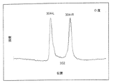
図3A及び図3Bは、図1A及び図1Bに示すアンダカットされているアンダカット造作170の実験的な電子走査を示す。図3Aにおいては、ビームの傾きは0度であり、図3Bでは6.6度であった。図3Aと図3Bのいずれも、アンダカット造作170の領域の位置、アンダカット造作に対する電子線の照射位置と電子線強度の関係を示している。図3Aと図3Bの電子走査では、試料の破壊が避けがたいものではないため、図1Aと図1Bの破壊的なFIB断面形成に先だって実施された。本発明を利用することにより、破壊的なFIBによる断面形成を利用することなくアンダカット角を測定することができる。
3A and 3B show an experimental electronic scan of the
図3Aからわかるように、造作170に関する電子線強度プロファイル302は比較的対称的であるように見える。プロファイル302の左側にはピーク304-Lがあり、また右側には左側のピークとほぼ同じ寸法のピーク304-Rがある。示す対称性により、一次電子ビームの入射角が0度であったことが予想される。
As can be seen from FIG. 3A, the
一方、図3Bにおいては、造作170に関する電子線強度プロファイル312は非対照であるように見える。右側のピーク314-Rは、左側のピーク314-Lに比べて実質上高い。本発明者等は、プロファイルのこの非対称性は、電子ビームが、右の側壁のアンダカット角(おおよそ4度)を超える角度(おおよそ6.6度)で入射しているためであると考えている。つまり、入射ビームが、右の側壁を直接照射したために、非常に多くの散乱電子が放出されたと考えられる。本発明の実施態様によれば、図3A及び図3Bから、アンダカット角はおおよそ0度と6.6度の間の角度であると特定できる。
On the other hand, in FIG. 3B, the electron
図3Bのピークの幅が図3Aのピークの幅よりも広いことに注目されたい。ピークの幅のこの広がりは、SEMにおいて入射ビームが傾いた際に生じる検出像のぶれに対応する。このぶれは、右側のピークの強度と左側のピークの強度との間に非対称性をもたらし、走査した像から視覚的に検出するのを困難にすると考えられる。そのため、本発明の好ましい実施態様では、走査したデータを定量的に分析する。 Note that the peak width of FIG. 3B is wider than the peak width of FIG. 3A. This broadening of the peak width corresponds to the blurring of the detected image that occurs when the incident beam is tilted in the SEM. This blur is believed to cause asymmetry between the intensity of the right and left peaks, making it difficult to visually detect from the scanned image. Therefore, in a preferred embodiment of the present invention, the scanned data is analyzed quantitatively.
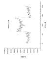
図4Aは、本発明の実施態様による、左側のアンダカット角を測定するために、異なる一連の入射角で電子走査して得られたデータの分析結果を示すグラフである。y軸は、左側のピーク強度I(左)と右側のピーク強度I(右)の比率(I(左)/I(右))を示す。x軸は、一次ビームの入射角(ふれ角)を度で示す。好ましい実施態様では、ピーク強度はピークの高さで測定される。しかしながら、他の実施態様においては、積分したピーク面積を利用してピーク強度を測定することも可能である。図4Aのグラフにおいて、入射角が約-4度でデータの勾配が不連続となっていることがわかる。これは、左の側壁のアンダカット角がおおよそ4度であることを示している。この結果は、FIB断面の測定による左の側壁のアンダカット角が約5度であることと良く一致している。 FIG. 4A is a graph showing analysis results of data obtained by electronic scanning at different series of incident angles to measure the left undercut angle according to an embodiment of the present invention. The y-axis indicates the ratio (I (left) / I (right)) between the left peak intensity I (left) and the right peak intensity I (right). The x-axis indicates the incident angle (deflection angle) of the primary beam in degrees. In a preferred embodiment, peak intensity is measured at the peak height. However, in other embodiments, the peak intensity can be measured using the integrated peak area. In the graph of FIG. 4A, it can be seen that the incident angle is about −4 degrees and the data gradient is discontinuous. This indicates that the undercut angle of the left side wall is approximately 4 degrees. This result agrees well with the undercut angle of the left side wall measured by FIB cross section of about 5 degrees.
図4Bは、本発明の実施態様による、右側のアンダカット角を測定するために、異なる一連の入射角で電子走査して得られたデータの分析結果を示すグラフである。y軸は、右側のピーク強度I(右)と左側のピーク強度I(左)の比率(I(右)/I(左))を示す。x軸は、一次ビームの入射角(ふれ角)を度で示す。図4Bのグラフにおいて、入射角が約+3度でデータの勾配が不連続となっていることがわかる。これは、右の側壁のアンダカット角がおおよそ3度であることを示している。この結果は、FIB断面で測定された、左の側壁のアンダカット角が約2度であることと良く一致している。 FIG. 4B is a graph showing analysis results of data obtained by electronic scanning at different series of incident angles to measure the right undercut angle according to an embodiment of the present invention. The y-axis indicates the ratio (I (right) / I (left)) between the right peak intensity I (right) and the left peak intensity I (left). The x-axis indicates the incident angle (deflection angle) of the primary beam in degrees. In the graph of FIG. 4B, it can be seen that the incident angle is about +3 degrees and the data gradient is discontinuous. This indicates that the undercut angle of the right side wall is approximately 3 degrees. This result agrees well with the undercut angle of the left side wall, measured on the FIB cross section, of about 2 degrees.
図5A〜図5Dは、両側にそれぞれ10度のアンダカット角を有する仮想的な造作に対して模擬的に行った電子走査の結果を示す。これら図面のそれぞれは、x軸上の位置の関数として、y軸に電子線の強度(任意単位)を表示している。図5Aは、6度又はそれ以下の小さな入射角である場合に対応し、比較的対照的なプロファイルを示している。図5Bは、入射角が11度である場合に対応し、右側のピークが左側のピークよりも高く、非対称なプロファイルを示している。図5Cは、入射角が17度である場合に対応し、右側のピークが尚いっそう高く、非対称性が増大していることを示している。最後に、図5Dは、入射角が25度である場合に対応し、右側のピークが図5Cと比較して低く、非対称性が低減していることを示している。従って図5Dは、極めて大きな角度では、非対称性が増大し続けないことを示している。 FIGS. 5A to 5D show the results of electronic scanning that was simulated for a hypothetical feature having undercut angles of 10 degrees on each side. Each of these drawings displays the electron beam intensity (in arbitrary units) on the y-axis as a function of position on the x-axis. FIG. 5A shows a relatively contrasting profile corresponding to the case of small incident angles of 6 degrees or less. FIG. 5B corresponds to the case where the incident angle is 11 degrees, and the right peak is higher than the left peak, and shows an asymmetric profile. FIG. 5C corresponds to the case where the angle of incidence is 17 degrees, showing that the peak on the right is even higher and the asymmetry is increased. Finally, FIG. 5D corresponds to the case where the incident angle is 25 degrees, and the right-side peak is low compared to FIG. 5C, indicating that the asymmetry is reduced. Therefore, FIG. 5D shows that at very large angles, asymmetry does not continue to increase.
図6は、本発明の実施態様に従った、図5A〜図5Dの模擬データの分析結果を示すグラフである。図6中のデータ点は、0度(図5Aから)、6度(図5Aから)、11度(図5Bから)、17度(図5Cから)及び25度(図5Dから)である。図6からわかるように、アンダカット角は6度と11度の間の角度である。模擬実験がアンダカット角が10度のものを使用して行われているため、これは良好な結果である。もちろん、より正確なアンダカット角の測定を行うために、それぞれがより近い角度でもって模擬実験を行うことも可能である。 FIG. 6 is a graph showing the analysis results of the simulated data of FIGS. 5A to 5D according to the embodiment of the present invention. The data points in FIG. 6 are 0 degrees (from FIG. 5A), 6 degrees (from FIG. 5A), 11 degrees (from FIG. 5B), 17 degrees (from FIG. 5C) and 25 degrees (from FIG. 5D). As can be seen from FIG. 6, the undercut angle is between 6 and 11 degrees. This is a good result because the simulation was conducted using an undercut angle of 10 degrees. Of course, in order to perform a more accurate measurement of the undercut angle, it is possible to perform a simulation experiment at angles closer to each other.
本発明を利用することができるSEMシステムの例として、走査電子顕微鏡(SEM)システムを図7と図8に示す。本発明は、他の形式のSEMシステムにおいても同様に利用することができる。 As an example of an SEM system in which the present invention can be used, a scanning electron microscope (SEM) system is shown in FIGS. The present invention can be used in other types of SEM systems as well.
図7に示すSEMシステム10は、臨界寸法を測定するのに特に適しており、このシステムは、発明の名称が"Electron Beam Does Control for Scanning Electron Microscopy and Critical Dimension Measurement Instruments"であり、カリフォルニア州のサンノゼのKLA-Tencor Corporationに譲渡された、Richardsonらの米国特許第5,869,833号に詳細に開示されている。この米国特許第5,869,833号公報(Richardson特許)の開示は、参照することにより、その内容を全て本願発明に組み入れる。
The
図7のSEM 10は、電子ビーム源12、集束カラム及びレンズアセンブリ14及び走査コントローラ16を含む。走査コントローラ16は、試料20の選択領域全体にわたって電子ビームを走査する。またSEM 10は、試料20からの二次電子及び後方散乱電子を検出するための検出器サブシステム24を含む。
The
SEMシステム10の最上部にある電子ビーム源12が、電子ビーム34を生成する。使用可能な一手段は、電源32で発生した表面電界で加速された電子を有する熱電界エミッターからなる電子源36を含む。代替的な電子源の実施態様を代わりに採用することができる。ビーム源12内で電子源36によって放出された電子は、次いで電極38と源レンズ39(いずれもまた電源32によって制御される)を直接通過し、集束カラム及びレンズアセンブリ14に入って、試料20に誘導される電子ビーム34を形成する。
An
集束カラム及びレンズアセンブリ14において、電子ビーム34は、アパーチャ41を通過し、それによりビーム電流が低減される。例えばビーム電流は、おおよそ300pA(ピコアンペア)から、5〜100pAの範囲にまで低減され、34'の符号を付された電子ビームが形成される。電子ビーム34'は、次いで磁気コイル43と磁極片44を含み強力な磁界を発生させる対物レンズ42を通過する。この磁界は、試料20に誘導する際に、ビーム34'を、例えば約5nm(ナノメートル)であるようなスポットサイズを有する電子ビーム18に集束させるのに使用される。試料20には、電子が試料20に接近する際にビーム18の電子を減速させる減速電界が作られるように、電源52によりバイアスを適用することができる。
In the focusing column and
操作において、電子ビーム18は、試料20全面にわたって走査されるラスターであってよく、また二次及び後方散乱電子信号28は検出器サブシステム24によって検出される。電子ビーム18と試料20の相互作用の結果、二次及び後方散乱電子28が放出され、対物レンズ42に向かって戻るように方向付けられる。電子28は放出されると、対物レンズ42を通って螺旋状に上昇し(磁界の結果)、次いでレンズ42内の磁界から離れると電子は検出器サブシステム24に向かって移動する。典型的には、試料20は、導電性、絶縁性又は半導体であるような様々な物質を含む。試料20内の副領域は、その副領域の造作を測定するための走査に特に重要である場合がある。画像プロセッサー及びディスプレイサブシステム26が、この副領域の画像を顕在化し得る。例えば試料20を半導体ウェーハとすることができ、そのウェーハの副領域をウェーハの回路ダイの一部分とすることができる。
In operation, the
検出器サブシステム24は、少なくとも、電子信号28を形成する二次及び後方散乱電子を検出するのに適したバンド幅を有するように選択される。例えば検出器サブシステム24は、マイクロチャネルプレート、マイクロ球形プレート、半導体ダイオード又はシンチレーター及び光電子倍増アセンブリを含む。図7に例示する検出器サブシステム24は、検出器55及びコレクタ極板56を含む。二次及び後方散乱電子信号28は、検出器55により受容され、さらにコレクタ極板56により収集される。コレクタ極板56は、画像プロセッサ及びディスプレイサブシステム26によって受信される信号を生成する。画像プロセッサ及びディスプレイサブシステム26は、信号が画像発生器59に入力される前に、増幅器58によって信号を増幅することができる。
The
試料20上の電子ビーム18の位置は、走査コントローラ16によって制御される。図7に例示する走査コントローラ16は、コイル43と磁極片44によって生じた磁界内に配置されている走査プレート45を含む。走査プレート45は、ラスター発生器48によって電力を供給され(ライン46と47の信号を介して)、試料20を横切るx方向及びy方向の両方に電子ビーム18を誘導する。
The position of the
図8に図示するSEMシステムは、発明の名称が"electron Beam Inspection System and Method"である、Meisbergerらの特許で、カリフォルニア州サンノゼのKLA-Tencor Corporationに譲渡された米国特許第5,578,821号に開示されている。米国特許第5,578,821号の開示(Meisberger特許)は、参照することにより、その内容を全て本願発明に組み入れる。 The SEM system illustrated in FIG. 8 is disclosed in US Pat. No. 5,578,821, assigned to KLA-Tencor Corporation of San Jose, Calif., By Meisberger et al., Whose title is “electron Beam Inspection System and Method”. ing. The disclosure of US Pat. No. 5,578,821 (Meisberger patent) is hereby incorporated by reference in its entirety.
図8は、電子ビーム検査のための電子光学カラム及び収集システムを介する一次電子、二次電子、後方散乱電子及び被送信電子の経路の、簡略化した概略図である。要するに、図8は、カラム内及び基体57の下方の様々な電子ビーム経路の概略を示す。電子は、電界放出陰極81から放射状に放出され、極小の点光源から発しているように見える。加速電界と集束レンズ磁界を組合せた作用のもとで、ビームは平行化され、平行ビームとなる。電子銃陽極アパーチャ87は、使用に適さない角度で放出された電子を遮蔽するが、一方遮蔽されない残留ビームは照射野制限アパーチャ99へと進む。上方の偏向板(図示せず)が、無収差化、共心化及び方向付けのために使用され、最終的なビームは断面が円形であり、要素105、106及び107から構成されている対物レンズ104の中央を通過することを確実にする。集束レンズ(図示せず)は、陰極81と照射野制限アパーチャ99により画定される軸に対して機械的に心合わせされる。偏向は、示される経路をたどり、それによって走査され、集束されたプローブ(基体との衝突点におけるビーム)が、対物レンズ42から放射される。
FIG. 8 is a simplified schematic diagram of the path of primary, secondary, backscattered and transmitted electrons through an electron optical column and collection system for electron beam inspection. In summary, FIG. 8 shows an overview of the various electron beam paths in the column and below the
高電圧モードでの操作において、ウィーンフィルター偏向板112及び113は、二次電子ビーム167を検出器117内へと偏向させる。部分的に透明なマスクが作像されると、透過ビーム108は、検出器129に衝突する前に、ビーム108を拡散させる電極システム123及び124を通過する。低電圧モードでの操作において、二次電子ビームは、より強力なウィーンフィルター偏向板によって、低圧二次電子検出器160に向かって方向付けされる。この場合の検出器は、高電圧で後方散乱の画像を作製するのに使用される検出器と同じとすることができる。このシステム及びその操作について、Meisberger特許にさらに詳細に開示されている。
In operation in the high voltage mode, the Wien
本発明の一実施態様によれば、一次電子ビームの入射角を、試料へビームを集束させる対物レンズにおける流れを適切に調整することによって変更することができる。本発明の別の実施態様によれば、一次電子ビームの入射角を、試料を保持する試料台を傾斜させることによって変更することができる。好都合なことに、この実施態様では、入射ビームが傾いた際に発生する走査画像のぶれを防ぐことができる。 According to one embodiment of the present invention, the incident angle of the primary electron beam can be changed by appropriately adjusting the flow in the objective lens that focuses the beam onto the sample. According to another embodiment of the present invention, the incident angle of the primary electron beam can be changed by inclining the sample stage holding the sample. Advantageously, this embodiment can prevent scan image blurring that occurs when the incident beam is tilted.
代替的な実施態様においては、ある範囲の角度における電子の検出を、アンダカット角を測定するのに使用することができる。そのような実施態様は、異なる散乱角における多数の電子検出器と、異なる散乱角における散乱電子を区別するための不均一な抽出用電界の適用を含む。多数の検出器は、大きな検出角度において、対象となる側壁が検出器の照準線内に直に入るように配向され、それによって直接的な照準線のない第1の検出器により検出されるビーム強度と、直接的な照準線を有する第2の検出器により検出されるビーム強度との間に不連続が生じる。この場合、測定されたアンダカット角は、不連続の発生が確認される検出角度に対応する。 In an alternative embodiment, detection of electrons at a range of angles can be used to measure the undercut angle. Such embodiments include a number of electronic detector at different scattering angles, the application of non-uniform extraction field for distinguishing the scattered electrons at different scattering angles. Many detectors are oriented so that at a large detection angle, the sidewall of interest is directly within the line of sight of the detector, so that the beam detected by the first detector without a direct line of sight There is a discontinuity between the intensity and the beam intensity detected by the second detector with a direct line of sight. In this case, the measured undercut angle corresponds to a detection angle at which occurrence of discontinuity is confirmed.
上述の説明において、数多くの特定の詳細を、本発明の実施態様の完全な理解をもたらすために提供した。しかしながら、例示した本発明の実施態様の上記説明は、本発明を網羅することも、あるいは開示された形態そのものに本発明を限定することも意図するものではない。当業者は、1つ又はより多くの具体的細部なしに、あるいはその他の方法、構成要素などと共に本発明が実施可能であることを認めるであろう。その他、本発明の不明瞭な理解を避けるため、周知の構造又は操作を詳細に示したり、あるいは説明したりしていない。本発明の具体的な実施態様及び例を、例示目的でここに説明しているが、当業者が認識するように、本発明の範囲内で様々な等価の変更が可能である。 In the above description, numerous specific details are provided to provide a thorough understanding of embodiments of the invention. However, the above description of illustrated embodiments of the invention is not intended to be exhaustive or to limit the invention to the precise form disclosed. Those skilled in the art will recognize that the invention may be practiced without one or more specific details, or with other methods, components, and the like. In other instances, well-known structures or operations are not shown or described in detail to avoid obscuring the present invention. While specific embodiments and examples of the invention have been described herein for purposes of illustration, as will be appreciated by those skilled in the art, various equivalent modifications are possible within the scope of the invention.
上述の詳細な説明を考慮することによって、本発明にそのような変更を行うことができる。本願の特許請求の範囲で使用される用語は、本明細書及び特許請求の範囲に開示の特定の実施態様に本発明を限定するものと解釈すべきではない。むしろ、本発明の範囲は、特許請求の範囲によって画定されるべきものであり、それは、特許請求の範囲を解釈するという確立されている原則に従うものと解釈される。 Such changes can be made to the invention in light of the above detailed description. The terms used in the following claims should not be construed to limit the invention to the specific embodiments disclosed in the specification and the claims. Rather, the scope of the present invention is to be defined by the following claims, which are to be construed in accordance with the established principles of interpreting the scope of the claims.
10 SEMシステム
12 電子ビーム源
14 レンズアセンブリ
16 走査コントローラ
20 試料
24 検出器サブシステム
28 後方散乱電子
34 電子ビーム
36 電子源
38 電極
39 源レンズ
41 アパーチャ
42 対物レンズ
43 磁気コイル
44 磁極片
45 走査プレート
55 検出器
56 コレクタ電極
58 増幅器
10
Claims (19)
ある入射角の一次電子ビームで前記構造要素を照射するステップ、
前記一次電子ビームの前記入射角を一組の角度にわたって変更するステップ、
前記一組の角度におけるそれぞれの入射角に対して、前記構造要素の第1の側壁と反対側の第2の側壁からの散乱電子のピーク強度を測定するステップ、
前記第1の側壁と前記第2の側壁の前記ピーク強度の比率における勾配の不連続を前記入射角の関数として求めるステップを含み、
測定されるアンダカット角が、前記不連続の発生が確認された入射角に対応する、
方法。 A method for measuring an undercut of a structural element of a sample using a scanning electron microscope (SEM),
Illuminating the structural element with a primary electron beam at an incident angle;
Changing the incident angle of the primary electron beam over a set of angles;
Measuring the peak intensity of scattered electrons from a second sidewall opposite the first sidewall of the structural element for each incident angle in the set of angles;
Look including the step of determining the discontinuities of slope in the ratio of the peak intensity of the second side wall and said first side wall as a function of the incident angle,
The measured undercut angle corresponds to the incident angle at which the occurrence of the discontinuity was confirmed,
Method.
ある入射角の一次電子ビームで前記構造要素を照射するステップ、
複数の検出器により、一組の散乱角における前記構造要素の第1の側壁と反対側の第2の側壁からの散乱電子のピーク強度を測定するステップ、
前記第1の側壁と前記第2の側壁の前記ピーク強度の比率における勾配の不連続を前記散乱角の関数として求めるステップを含み、
測定されるアンダカット角が、前記不連続の発生が確認された検出角度に対応する、
方法。 A method for measuring an undercut of a structural element on a sample using a scanning electron microscope (SEM),
Illuminating the structural element with a primary electron beam at an incident angle;
Measuring the peak intensity of scattered electrons from a second sidewall opposite the first sidewall of the structural element at a set of scattering angles with a plurality of detectors;
Look including the step of determining the discontinuities of slope in the ratio of the peak intensity of the second side wall and said first side wall as a function of the scattering angle,
The measured undercut angle corresponds to the detected angle at which the occurrence of the discontinuity was confirmed ,
Method.
ある入射角の一次電子ビームで前記構造要素を照射するための電子照射システム、
前記一次電子ビームの前記入射角を一組の角度にわたって変更するための機構、
前記一組の角度におけるそれぞれの入射角に対して、前記構造要素の第1の側壁と反対側の第2の側壁からの散乱電子のピーク強度を測定するための検出器、
前記第1の側壁と前記第2の側壁の前記ピーク強度の比率における勾配の不連続を前記入射角の関数として求めるためのプロセッサーを含み、
測定されるアンダカット角が、前記不連続の発生が確認された入射角に対応する、
走査電子顕微鏡。 A scanning electron microscope (SEM) for measuring an undercut of a structural element on a sample,
An electron irradiation system for irradiating the structural element with a primary electron beam at an incident angle;
A mechanism for changing the angle of incidence of the primary electron beam over a set of angles;
A detector for measuring the peak intensity of scattered electrons from a second side wall opposite the first side wall of the structural element for each angle of incidence in the set of angles;
A processor for determining a gradient discontinuity in the ratio of the peak intensity of the first sidewall and the second sidewall as a function of the angle of incidence;
The measured undercut angle corresponds to the incident angle at which the occurrence of the discontinuity was confirmed,
Scanning electron microscope.
ある入射角の一次電子ビームで前記構造要素を照射するための手段、
前記一次電子ビームの前記入射角を一組の角度にわたって変更するための手段、
前記一組の角度におけるそれぞれの入射角に対して、前記構造要素の第1の側壁と反対側の第2の側壁からの散乱電子のピーク強度を測定するための手段、
前記第1の側壁と前記第2の側壁の前記ピーク強度の比率における勾配の不連続を前記入射角の関数として求めるための手段を含み、
測定されるアンダカット角が、前記不連続の発生が確認された入射角に対応する、
装置。 An apparatus for measuring an undercut of a structural element on a sample,
Means for irradiating the structural element with a primary electron beam at an angle of incidence;
Means for changing the angle of incidence of the primary electron beam over a set of angles;
Means for measuring the peak intensity of scattered electrons from a second sidewall opposite the first sidewall of the structural element for each incident angle in the set of angles;
Look including means for determining a discontinuous gradient in the ratio of the peak intensity of the second side wall and said first side wall as a function of the incident angle,
The measured undercut angle corresponds to the incident angle at which the occurrence of the discontinuity was confirmed,
apparatus.
Applications Claiming Priority (1)
| Application Number | Priority Date | Filing Date | Title |
|---|---|---|---|
| US10/186,797 US6670612B1 (en) | 2002-07-01 | 2002-07-01 | Undercut measurement using SEM |
Publications (3)
| Publication Number | Publication Date |
|---|---|
| JP2004132956A JP2004132956A (en) | 2004-04-30 |
| JP2004132956A5 JP2004132956A5 (en) | 2009-12-03 |
| JP4469572B2 true JP4469572B2 (en) | 2010-05-26 |
Family
ID=29735250
Family Applications (1)
| Application Number | Title | Priority Date | Filing Date |
|---|---|---|---|
| JP2003270078A Expired - Fee Related JP4469572B2 (en) | 2002-07-01 | 2003-07-01 | Undercut measurement method using SEM |
Country Status (2)
| Country | Link |
|---|---|
| US (1) | US6670612B1 (en) |
| JP (1) | JP4469572B2 (en) |
Cited By (1)
| Publication number | Priority date | Publication date | Assignee | Title |
|---|---|---|---|---|
| CN104508460A (en) * | 2012-06-05 | 2015-04-08 | B-纳米股份有限公司 | A system and method for performing analysis of materials in a non-vacuum environment using an electron microscope |
Families Citing this family (9)
| Publication number | Priority date | Publication date | Assignee | Title |
|---|---|---|---|---|
| AU2003263776A1 (en) * | 2002-07-11 | 2004-02-02 | Applied Materials Israel, Ltd | Method and apparatus for measuring critical dimensions with a particle beam |
| ATE526038T1 (en) * | 2003-03-28 | 2011-10-15 | Innovational Holdings Llc | IMPLANTABLE MEDICAL DEVICE WITH CONTINUOUS MEDIUM CONCENTRATION DISTANCE |
| DE102004004597B4 (en) * | 2004-01-29 | 2008-08-07 | Qimonda Ag | Method for measuring a structure on a semiconductor wafer with a scanning electron microscope |
| US7355709B1 (en) | 2004-02-23 | 2008-04-08 | Kla-Tencor Technologies Corp. | Methods and systems for optical and non-optical measurements of a substrate |
| JP5367549B2 (en) | 2009-12-07 | 2013-12-11 | 株式会社東芝 | Substrate measurement method |
| US20160336143A1 (en) * | 2015-05-15 | 2016-11-17 | Kabushiki Kaisha Toshiba | Charged particle beam apparatus and method of calibrating sample position |
| TWI797449B (en) * | 2019-05-21 | 2023-04-01 | 美商應用材料股份有限公司 | Enhanced cross sectional features measurement methodology and system |
| US11264202B2 (en) * | 2020-05-18 | 2022-03-01 | Applied Materials Israel Ltd. | Generating three dimensional information regarding structural elements of a specimen |
| CN112563149B (en) * | 2020-12-11 | 2023-12-01 | 苏州工业园区纳米产业技术研究院有限公司 | Method for accurately measuring drilling size and stripping process |
Family Cites Families (16)
| Publication number | Priority date | Publication date | Assignee | Title |
|---|---|---|---|---|
| JPS56114269A (en) * | 1980-02-15 | 1981-09-08 | Internatl Precision Inc | Scanning type electronic microscope |
| JPH01311551A (en) * | 1988-06-08 | 1989-12-15 | Toshiba Corp | Pattern shape measuring device |
| JPH02249908A (en) * | 1989-03-24 | 1990-10-05 | Dainippon Printing Co Ltd | Method for inspecting resist pattern |
| JPH07111336B2 (en) * | 1990-02-07 | 1995-11-29 | 株式会社東芝 | Pattern dimension measuring method and device |
| US6411377B1 (en) * | 1991-04-02 | 2002-06-25 | Hitachi, Ltd. | Optical apparatus for defect and particle size inspection |
| JP3730263B2 (en) * | 1992-05-27 | 2005-12-21 | ケーエルエー・インストルメンツ・コーポレーション | Apparatus and method for automatic substrate inspection using charged particle beam |
| JP3265724B2 (en) * | 1993-07-14 | 2002-03-18 | 株式会社日立製作所 | Charged particle beam equipment |
| US5739909A (en) * | 1995-10-10 | 1998-04-14 | Lucent Technologies Inc. | Measurement and control of linewidths in periodic structures using spectroscopic ellipsometry |
| US5869833A (en) * | 1997-01-16 | 1999-02-09 | Kla-Tencor Corporation | Electron beam dose control for scanning electron microscopy and critical dimension measurement instruments |
| US6066849A (en) * | 1997-01-16 | 2000-05-23 | Kla Tencor | Scanning electron beam microscope |
| US6054710A (en) * | 1997-12-18 | 2000-04-25 | Cypress Semiconductor Corp. | Method and apparatus for obtaining two- or three-dimensional information from scanning electron microscopy |
| US6031614A (en) * | 1998-12-02 | 2000-02-29 | Siemens Aktiengesellschaft | Measurement system and method for measuring critical dimensions using ellipsometry |
| JP4361661B2 (en) * | 2000-03-24 | 2009-11-11 | 富士通マイクロエレクトロニクス株式会社 | Line width measurement method |
| US6472662B1 (en) * | 2000-08-30 | 2002-10-29 | International Business Machines Corporation | Automated method for determining several critical dimension properties from scanning electron microscope by using several tilted beam or sample scans |
| US6911349B2 (en) * | 2001-02-16 | 2005-06-28 | Boxer Cross Inc. | Evaluating sidewall coverage in a semiconductor wafer |
| JP4094327B2 (en) * | 2002-04-10 | 2008-06-04 | 株式会社日立ハイテクノロジーズ | PATTERN MEASURING METHOD, PATTERN MEASURING DEVICE, AND PATTERN PROCESS CONTROL METHOD |
-
2002
- 2002-07-01 US US10/186,797 patent/US6670612B1/en not_active Expired - Lifetime
-
2003
- 2003-07-01 JP JP2003270078A patent/JP4469572B2/en not_active Expired - Fee Related
Cited By (2)
| Publication number | Priority date | Publication date | Assignee | Title |
|---|---|---|---|---|
| CN104508460A (en) * | 2012-06-05 | 2015-04-08 | B-纳米股份有限公司 | A system and method for performing analysis of materials in a non-vacuum environment using an electron microscope |
| CN104508460B (en) * | 2012-06-05 | 2017-09-12 | B-纳米股份有限公司 | The system and method analyzed using electron microscope the material for being present in non-vacuum environment |
Also Published As
| Publication number | Publication date |
|---|---|
| US20040000638A1 (en) | 2004-01-01 |
| US6670612B1 (en) | 2003-12-30 |
| JP2004132956A (en) | 2004-04-30 |
Similar Documents
| Publication | Publication Date | Title |
|---|---|---|
| JP6091573B2 (en) | Sample observation method and apparatus | |
| US10777383B2 (en) | Method for alignment of a light beam to a charged particle beam | |
| TWI420096B (en) | An e-beam defect review system | |
| JP5227643B2 (en) | An electron beam application device that enables observation with high resolution and high contrast | |
| KR102373865B1 (en) | Charged particle beam specimen inspection system and method for operation thereof | |
| US7202476B2 (en) | Charged-particle beam instrument | |
| JP4920385B2 (en) | Charged particle beam apparatus, scanning electron microscope, and sample observation method | |
| JP2007207688A (en) | Mirror electron microscope, and inspection device using mirror electron microscope | |
| JP4469572B2 (en) | Undercut measurement method using SEM | |
| JP2001357808A (en) | Device and method for inspecting circuit pattern | |
| US11626267B2 (en) | Back-scatter electrons (BSE) imaging with a SEM in tilted mode using cap bias voltage | |
| JP2004513477A (en) | SEM with adjustable final electrode for electrostatic objective | |
| US20230133404A1 (en) | Method of inspecting a sample, and multi-electron beam inspection system | |
| US8008629B2 (en) | Charged particle beam device and method for inspecting specimen | |
| JP3986032B2 (en) | electronic microscope | |
| JP2015170593A (en) | analyzer | |
| JP4658783B2 (en) | Sample image forming method | |
| JP5544439B2 (en) | Charged particle beam equipment | |
| JPH0982261A (en) | Electron microscope | |
| JP4334159B2 (en) | Substrate inspection system and substrate inspection method | |
| US20020079449A1 (en) | SEM having a detector surface segmented into a number of separate regions | |
| JP3814968B2 (en) | Inspection device | |
| JP2007220317A (en) | Electron beam inspection method and device | |
| TW202338889A (en) | Back-scatter electrons (bse) imaging with a sem in tilted mode using cap bias voltage | |
| JP2005024564A (en) | Test method and test apparatus using electron beam |
Legal Events
| Date | Code | Title | Description |
|---|---|---|---|
| A621 | Written request for application examination |
Free format text: JAPANESE INTERMEDIATE CODE: A621 Effective date: 20060601 |
|
| A131 | Notification of reasons for refusal |
Free format text: JAPANESE INTERMEDIATE CODE: A131 Effective date: 20090428 |
|
| A601 | Written request for extension of time |
Free format text: JAPANESE INTERMEDIATE CODE: A601 Effective date: 20090728 |
|
| A602 | Written permission of extension of time |
Free format text: JAPANESE INTERMEDIATE CODE: A602 Effective date: 20090731 |
|
| A524 | Written submission of copy of amendment under article 19 pct |
Free format text: JAPANESE INTERMEDIATE CODE: A524 Effective date: 20091009 |
|
| A131 | Notification of reasons for refusal |
Free format text: JAPANESE INTERMEDIATE CODE: A131 Effective date: 20091110 |
|
| A521 | Request for written amendment filed |
Free format text: JAPANESE INTERMEDIATE CODE: A523 Effective date: 20091110 |
|
| TRDD | Decision of grant or rejection written | ||
| A01 | Written decision to grant a patent or to grant a registration (utility model) |
Free format text: JAPANESE INTERMEDIATE CODE: A01 Effective date: 20100223 |
|
| A01 | Written decision to grant a patent or to grant a registration (utility model) |
Free format text: JAPANESE INTERMEDIATE CODE: A01 |
|
| A61 | First payment of annual fees (during grant procedure) |
Free format text: JAPANESE INTERMEDIATE CODE: A61 Effective date: 20100301 |
|
| R150 | Certificate of patent or registration of utility model |
Ref document number: 4469572 Country of ref document: JP Free format text: JAPANESE INTERMEDIATE CODE: R150 Free format text: JAPANESE INTERMEDIATE CODE: R150 |
|
| FPAY | Renewal fee payment (event date is renewal date of database) |
Free format text: PAYMENT UNTIL: 20130305 Year of fee payment: 3 |
|
| FPAY | Renewal fee payment (event date is renewal date of database) |
Free format text: PAYMENT UNTIL: 20130305 Year of fee payment: 3 |
|
| FPAY | Renewal fee payment (event date is renewal date of database) |
Free format text: PAYMENT UNTIL: 20140305 Year of fee payment: 4 |
|
| R250 | Receipt of annual fees |
Free format text: JAPANESE INTERMEDIATE CODE: R250 |
|
| R250 | Receipt of annual fees |
Free format text: JAPANESE INTERMEDIATE CODE: R250 |
|
| R250 | Receipt of annual fees |
Free format text: JAPANESE INTERMEDIATE CODE: R250 |
|
| R250 | Receipt of annual fees |
Free format text: JAPANESE INTERMEDIATE CODE: R250 |
|
| R250 | Receipt of annual fees |
Free format text: JAPANESE INTERMEDIATE CODE: R250 |
|
| R250 | Receipt of annual fees |
Free format text: JAPANESE INTERMEDIATE CODE: R250 |
|
| LAPS | Cancellation because of no payment of annual fees |