JP4469552B2 - Thick single crystal diamond layer, method of making it and gemstone formed from that layer - Google Patents
Thick single crystal diamond layer, method of making it and gemstone formed from that layer Download PDFInfo
- Publication number
- JP4469552B2 JP4469552B2 JP2002510742A JP2002510742A JP4469552B2 JP 4469552 B2 JP4469552 B2 JP 4469552B2 JP 2002510742 A JP2002510742 A JP 2002510742A JP 2002510742 A JP2002510742 A JP 2002510742A JP 4469552 B2 JP4469552 B2 JP 4469552B2
- Authority
- JP
- Japan
- Prior art keywords
- diamond
- layer
- single crystal
- cvd diamond
- etching
- Prior art date
- Legal status (The legal status is an assumption and is not a legal conclusion. Google has not performed a legal analysis and makes no representation as to the accuracy of the status listed.)
- Expired - Lifetime
Links
- 239000010432 diamond Substances 0.000 title claims abstract description 141
- 229910003460 diamond Inorganic materials 0.000 title claims abstract description 132
- 239000013078 crystal Substances 0.000 title claims abstract description 47
- 239000010437 gem Substances 0.000 title claims abstract description 12
- 229910001751 gemstone Inorganic materials 0.000 title claims abstract description 11
- 238000004519 manufacturing process Methods 0.000 title claims description 11
- 238000000034 method Methods 0.000 claims abstract description 66
- 239000000758 substrate Substances 0.000 claims abstract description 56
- IJGRMHOSHXDMSA-UHFFFAOYSA-N Atomic nitrogen Chemical compound N#N IJGRMHOSHXDMSA-UHFFFAOYSA-N 0.000 claims abstract description 51
- 230000007547 defect Effects 0.000 claims abstract description 42
- 229910052757 nitrogen Inorganic materials 0.000 claims abstract description 27
- 239000007789 gas Substances 0.000 claims description 41
- 238000005530 etching Methods 0.000 claims description 30
- QVGXLLKOCUKJST-UHFFFAOYSA-N atomic oxygen Chemical compound [O] QVGXLLKOCUKJST-UHFFFAOYSA-N 0.000 claims description 20
- 239000001301 oxygen Substances 0.000 claims description 20
- 229910052760 oxygen Inorganic materials 0.000 claims description 20
- UFHFLCQGNIYNRP-UHFFFAOYSA-N Hydrogen Chemical compound [H][H] UFHFLCQGNIYNRP-UHFFFAOYSA-N 0.000 claims description 19
- 239000001257 hydrogen Substances 0.000 claims description 19
- 229910052739 hydrogen Inorganic materials 0.000 claims description 19
- 230000005684 electric field Effects 0.000 claims description 18
- XKRFYHLGVUSROY-UHFFFAOYSA-N Argon Chemical compound [Ar] XKRFYHLGVUSROY-UHFFFAOYSA-N 0.000 claims description 16
- 229910052786 argon Inorganic materials 0.000 claims description 11
- 239000004575 stone Substances 0.000 claims description 11
- 238000001020 plasma etching Methods 0.000 claims description 9
- 238000011065 in-situ storage Methods 0.000 claims description 6
- 238000010494 dissociation reaction Methods 0.000 claims description 4
- 230000005593 dissociations Effects 0.000 claims description 4
- 239000000523 sample Substances 0.000 description 36
- 239000002969 artificial stone Substances 0.000 description 18
- 239000000463 material Substances 0.000 description 16
- 238000004817 gas chromatography Methods 0.000 description 15
- 239000012535 impurity Substances 0.000 description 14
- 230000003287 optical effect Effects 0.000 description 14
- 230000005284 excitation Effects 0.000 description 10
- 238000012545 processing Methods 0.000 description 10
- 238000001069 Raman spectroscopy Methods 0.000 description 9
- 230000015572 biosynthetic process Effects 0.000 description 9
- 238000005136 cathodoluminescence Methods 0.000 description 9
- -1 Monosubstituted nitrogen Chemical class 0.000 description 8
- 238000005259 measurement Methods 0.000 description 8
- OKTJSMMVPCPJKN-UHFFFAOYSA-N Carbon Chemical compound [C] OKTJSMMVPCPJKN-UHFFFAOYSA-N 0.000 description 7
- 229910052799 carbon Inorganic materials 0.000 description 7
- 239000002800 charge carrier Substances 0.000 description 7
- 238000001237 Raman spectrum Methods 0.000 description 6
- 238000000103 photoluminescence spectrum Methods 0.000 description 6
- 238000003786 synthesis reaction Methods 0.000 description 6
- 238000002474 experimental method Methods 0.000 description 5
- 239000000203 mixture Substances 0.000 description 5
- 238000005086 pumping Methods 0.000 description 5
- 230000005855 radiation Effects 0.000 description 5
- 238000001228 spectrum Methods 0.000 description 5
- 238000002835 absorbance Methods 0.000 description 4
- 238000010521 absorption reaction Methods 0.000 description 4
- 238000000862 absorption spectrum Methods 0.000 description 4
- 238000001362 electron spin resonance spectrum Methods 0.000 description 4
- 229910052736 halogen Inorganic materials 0.000 description 4
- 150000002367 halogens Chemical class 0.000 description 4
- 239000002245 particle Substances 0.000 description 4
- 238000005498 polishing Methods 0.000 description 4
- 230000037452 priming Effects 0.000 description 4
- 239000000126 substance Substances 0.000 description 4
- 238000012546 transfer Methods 0.000 description 4
- 238000004435 EPR spectroscopy Methods 0.000 description 3
- 241000656145 Thyrsites atun Species 0.000 description 3
- 239000012159 carrier gas Substances 0.000 description 3
- 239000011261 inert gas Substances 0.000 description 3
- 238000002347 injection Methods 0.000 description 3
- 239000007924 injection Substances 0.000 description 3
- 150000002829 nitrogen Chemical class 0.000 description 3
- 238000005424 photoluminescence Methods 0.000 description 3
- 238000005070 sampling Methods 0.000 description 3
- 238000000926 separation method Methods 0.000 description 3
- WFKWXMTUELFFGS-UHFFFAOYSA-N tungsten Chemical compound [W] WFKWXMTUELFFGS-UHFFFAOYSA-N 0.000 description 3
- 229910052721 tungsten Inorganic materials 0.000 description 3
- 239000010937 tungsten Substances 0.000 description 3
- 238000004458 analytical method Methods 0.000 description 2
- 230000015556 catabolic process Effects 0.000 description 2
- 230000001419 dependent effect Effects 0.000 description 2
- 238000000151 deposition Methods 0.000 description 2
- 238000013461 design Methods 0.000 description 2
- 238000001514 detection method Methods 0.000 description 2
- 230000001747 exhibiting effect Effects 0.000 description 2
- 238000001036 glow-discharge mass spectrometry Methods 0.000 description 2
- 239000010931 gold Substances 0.000 description 2
- 238000012544 monitoring process Methods 0.000 description 2
- 230000035515 penetration Effects 0.000 description 2
- BASFCYQUMIYNBI-UHFFFAOYSA-N platinum Chemical compound [Pt] BASFCYQUMIYNBI-UHFFFAOYSA-N 0.000 description 2
- 238000000746 purification Methods 0.000 description 2
- 239000013074 reference sample Substances 0.000 description 2
- 238000001004 secondary ion mass spectrometry Methods 0.000 description 2
- 230000003746 surface roughness Effects 0.000 description 2
- 230000002194 synthesizing effect Effects 0.000 description 2
- 238000012360 testing method Methods 0.000 description 2
- ZOXJGFHDIHLPTG-UHFFFAOYSA-N Boron Chemical compound [B] ZOXJGFHDIHLPTG-UHFFFAOYSA-N 0.000 description 1
- 239000004215 Carbon black (E152) Substances 0.000 description 1
- RYGMFSIKBFXOCR-UHFFFAOYSA-N Copper Chemical compound [Cu] RYGMFSIKBFXOCR-UHFFFAOYSA-N 0.000 description 1
- YZCKVEUIGOORGS-OUBTZVSYSA-N Deuterium Chemical compound [2H] YZCKVEUIGOORGS-OUBTZVSYSA-N 0.000 description 1
- 101000993059 Homo sapiens Hereditary hemochromatosis protein Proteins 0.000 description 1
- ZOKXTWBITQBERF-UHFFFAOYSA-N Molybdenum Chemical compound [Mo] ZOKXTWBITQBERF-UHFFFAOYSA-N 0.000 description 1
- XUIMIQQOPSSXEZ-UHFFFAOYSA-N Silicon Chemical compound [Si] XUIMIQQOPSSXEZ-UHFFFAOYSA-N 0.000 description 1
- YZCKVEUIGOORGS-NJFSPNSNSA-N Tritium Chemical compound [3H] YZCKVEUIGOORGS-NJFSPNSNSA-N 0.000 description 1
- 230000002411 adverse Effects 0.000 description 1
- 229910052782 aluminium Inorganic materials 0.000 description 1
- XAGFODPZIPBFFR-UHFFFAOYSA-N aluminium Chemical compound [Al] XAGFODPZIPBFFR-UHFFFAOYSA-N 0.000 description 1
- 230000000903 blocking effect Effects 0.000 description 1
- 229910052796 boron Inorganic materials 0.000 description 1
- 238000005219 brazing Methods 0.000 description 1
- 238000012512 characterization method Methods 0.000 description 1
- 238000005229 chemical vapour deposition Methods 0.000 description 1
- 229910052804 chromium Inorganic materials 0.000 description 1
- 238000004140 cleaning Methods 0.000 description 1
- 239000011248 coating agent Substances 0.000 description 1
- 238000000576 coating method Methods 0.000 description 1
- 238000009838 combustion analysis Methods 0.000 description 1
- 238000002485 combustion reaction Methods 0.000 description 1
- 239000002131 composite material Substances 0.000 description 1
- 230000003750 conditioning effect Effects 0.000 description 1
- 239000000356 contaminant Substances 0.000 description 1
- 238000011109 contamination Methods 0.000 description 1
- 238000007796 conventional method Methods 0.000 description 1
- 229910052802 copper Inorganic materials 0.000 description 1
- 239000010949 copper Substances 0.000 description 1
- 238000005520 cutting process Methods 0.000 description 1
- 230000007423 decrease Effects 0.000 description 1
- 230000002950 deficient Effects 0.000 description 1
- 230000008021 deposition Effects 0.000 description 1
- 230000001627 detrimental effect Effects 0.000 description 1
- 229910052805 deuterium Inorganic materials 0.000 description 1
- 238000010790 dilution Methods 0.000 description 1
- 239000012895 dilution Substances 0.000 description 1
- 230000000694 effects Effects 0.000 description 1
- 238000010894 electron beam technology Methods 0.000 description 1
- 238000000295 emission spectrum Methods 0.000 description 1
- 238000005538 encapsulation Methods 0.000 description 1
- 238000005516 engineering process Methods 0.000 description 1
- 238000011156 evaluation Methods 0.000 description 1
- PCHJSUWPFVWCPO-UHFFFAOYSA-N gold Chemical compound [Au] PCHJSUWPFVWCPO-UHFFFAOYSA-N 0.000 description 1
- 229910052737 gold Inorganic materials 0.000 description 1
- 238000004442 gravimetric analysis Methods 0.000 description 1
- 150000008282 halocarbons Chemical class 0.000 description 1
- 239000001307 helium Substances 0.000 description 1
- 229910052734 helium Inorganic materials 0.000 description 1
- SWQJXJOGLNCZEY-UHFFFAOYSA-N helium atom Chemical compound [He] SWQJXJOGLNCZEY-UHFFFAOYSA-N 0.000 description 1
- 239000003097 hole (electron) Substances 0.000 description 1
- 229930195733 hydrocarbon Natural products 0.000 description 1
- 150000002430 hydrocarbons Chemical class 0.000 description 1
- 229910001872 inorganic gas Inorganic materials 0.000 description 1
- 238000005468 ion implantation Methods 0.000 description 1
- 150000002500 ions Chemical class 0.000 description 1
- 230000000155 isotopic effect Effects 0.000 description 1
- 239000007788 liquid Substances 0.000 description 1
- 238000004020 luminiscence type Methods 0.000 description 1
- 238000004949 mass spectrometry Methods 0.000 description 1
- 238000000691 measurement method Methods 0.000 description 1
- 230000007246 mechanism Effects 0.000 description 1
- 229910052751 metal Inorganic materials 0.000 description 1
- 239000002184 metal Substances 0.000 description 1
- 239000002808 molecular sieve Substances 0.000 description 1
- 229910052750 molybdenum Inorganic materials 0.000 description 1
- 239000011733 molybdenum Substances 0.000 description 1
- 229910052754 neon Inorganic materials 0.000 description 1
- GKAOGPIIYCISHV-UHFFFAOYSA-N neon atom Chemical compound [Ne] GKAOGPIIYCISHV-UHFFFAOYSA-N 0.000 description 1
- 230000005433 particle physics related processes and functions Effects 0.000 description 1
- 238000000206 photolithography Methods 0.000 description 1
- 238000009832 plasma treatment Methods 0.000 description 1
- 229910052697 platinum Inorganic materials 0.000 description 1
- 238000007517 polishing process Methods 0.000 description 1
- 239000011253 protective coating Substances 0.000 description 1
- 238000006862 quantum yield reaction Methods 0.000 description 1
- 238000010791 quenching Methods 0.000 description 1
- 230000000171 quenching effect Effects 0.000 description 1
- 230000004044 response Effects 0.000 description 1
- 230000002441 reversible effect Effects 0.000 description 1
- 230000035945 sensitivity Effects 0.000 description 1
- 229910052710 silicon Inorganic materials 0.000 description 1
- 239000010703 silicon Substances 0.000 description 1
- HBMJWWWQQXIZIP-UHFFFAOYSA-N silicon carbide Chemical compound [Si+]#[C-] HBMJWWWQQXIZIP-UHFFFAOYSA-N 0.000 description 1
- 229910010271 silicon carbide Inorganic materials 0.000 description 1
- URGAHOPLAPQHLN-UHFFFAOYSA-N sodium aluminosilicate Chemical compound [Na+].[Al+3].[O-][Si]([O-])=O.[O-][Si]([O-])=O URGAHOPLAPQHLN-UHFFFAOYSA-N 0.000 description 1
- 241000894007 species Species 0.000 description 1
- 230000003595 spectral effect Effects 0.000 description 1
- 229910001220 stainless steel Inorganic materials 0.000 description 1
- 239000010935 stainless steel Substances 0.000 description 1
- 230000007847 structural defect Effects 0.000 description 1
- 238000001308 synthesis method Methods 0.000 description 1
- 229920002994 synthetic fiber Polymers 0.000 description 1
- 229910052722 tritium Inorganic materials 0.000 description 1
- 238000011144 upstream manufacturing Methods 0.000 description 1
- 239000002699 waste material Substances 0.000 description 1
Images


Classifications
-
- C—CHEMISTRY; METALLURGY
- C30—CRYSTAL GROWTH
- C30B—SINGLE-CRYSTAL GROWTH; UNIDIRECTIONAL SOLIDIFICATION OF EUTECTIC MATERIAL OR UNIDIRECTIONAL DEMIXING OF EUTECTOID MATERIAL; REFINING BY ZONE-MELTING OF MATERIAL; PRODUCTION OF A HOMOGENEOUS POLYCRYSTALLINE MATERIAL WITH DEFINED STRUCTURE; SINGLE CRYSTALS OR HOMOGENEOUS POLYCRYSTALLINE MATERIAL WITH DEFINED STRUCTURE; AFTER-TREATMENT OF SINGLE CRYSTALS OR A HOMOGENEOUS POLYCRYSTALLINE MATERIAL WITH DEFINED STRUCTURE; APPARATUS THEREFOR
- C30B25/00—Single-crystal growth by chemical reaction of reactive gases, e.g. chemical vapour-deposition growth
- C30B25/02—Epitaxial-layer growth
- C30B25/10—Heating of the reaction chamber or the substrate
- C30B25/105—Heating of the reaction chamber or the substrate by irradiation or electric discharge
-
- A—HUMAN NECESSITIES
- A44—HABERDASHERY; JEWELLERY
- A44C—PERSONAL ADORNMENTS, e.g. JEWELLERY; COINS
- A44C17/00—Gems or the like
-
- B—PERFORMING OPERATIONS; TRANSPORTING
- B01—PHYSICAL OR CHEMICAL PROCESSES OR APPARATUS IN GENERAL
- B01J—CHEMICAL OR PHYSICAL PROCESSES, e.g. CATALYSIS OR COLLOID CHEMISTRY; THEIR RELEVANT APPARATUS
- B01J3/00—Processes of utilising sub-atmospheric or super-atmospheric pressure to effect chemical or physical change of matter; Apparatus therefor
- B01J3/06—Processes using ultra-high pressure, e.g. for the formation of diamonds; Apparatus therefor, e.g. moulds or dies
-
- C—CHEMISTRY; METALLURGY
- C30—CRYSTAL GROWTH
- C30B—SINGLE-CRYSTAL GROWTH; UNIDIRECTIONAL SOLIDIFICATION OF EUTECTIC MATERIAL OR UNIDIRECTIONAL DEMIXING OF EUTECTOID MATERIAL; REFINING BY ZONE-MELTING OF MATERIAL; PRODUCTION OF A HOMOGENEOUS POLYCRYSTALLINE MATERIAL WITH DEFINED STRUCTURE; SINGLE CRYSTALS OR HOMOGENEOUS POLYCRYSTALLINE MATERIAL WITH DEFINED STRUCTURE; AFTER-TREATMENT OF SINGLE CRYSTALS OR A HOMOGENEOUS POLYCRYSTALLINE MATERIAL WITH DEFINED STRUCTURE; APPARATUS THEREFOR
- C30B25/00—Single-crystal growth by chemical reaction of reactive gases, e.g. chemical vapour-deposition growth
- C30B25/02—Epitaxial-layer growth
- C30B25/18—Epitaxial-layer growth characterised by the substrate
- C30B25/20—Epitaxial-layer growth characterised by the substrate the substrate being of the same materials as the epitaxial layer
-
- C—CHEMISTRY; METALLURGY
- C30—CRYSTAL GROWTH
- C30B—SINGLE-CRYSTAL GROWTH; UNIDIRECTIONAL SOLIDIFICATION OF EUTECTIC MATERIAL OR UNIDIRECTIONAL DEMIXING OF EUTECTOID MATERIAL; REFINING BY ZONE-MELTING OF MATERIAL; PRODUCTION OF A HOMOGENEOUS POLYCRYSTALLINE MATERIAL WITH DEFINED STRUCTURE; SINGLE CRYSTALS OR HOMOGENEOUS POLYCRYSTALLINE MATERIAL WITH DEFINED STRUCTURE; AFTER-TREATMENT OF SINGLE CRYSTALS OR A HOMOGENEOUS POLYCRYSTALLINE MATERIAL WITH DEFINED STRUCTURE; APPARATUS THEREFOR
- C30B29/00—Single crystals or homogeneous polycrystalline material with defined structure characterised by the material or by their shape
- C30B29/02—Elements
- C30B29/04—Diamond
-
- B—PERFORMING OPERATIONS; TRANSPORTING
- B01—PHYSICAL OR CHEMICAL PROCESSES OR APPARATUS IN GENERAL
- B01J—CHEMICAL OR PHYSICAL PROCESSES, e.g. CATALYSIS OR COLLOID CHEMISTRY; THEIR RELEVANT APPARATUS
- B01J2203/00—Processes utilising sub- or super atmospheric pressure
- B01J2203/06—High pressure synthesis
- B01J2203/0605—Composition of the material to be processed
- B01J2203/062—Diamond
-
- B—PERFORMING OPERATIONS; TRANSPORTING
- B01—PHYSICAL OR CHEMICAL PROCESSES OR APPARATUS IN GENERAL
- B01J—CHEMICAL OR PHYSICAL PROCESSES, e.g. CATALYSIS OR COLLOID CHEMISTRY; THEIR RELEVANT APPARATUS
- B01J2203/00—Processes utilising sub- or super atmospheric pressure
- B01J2203/06—High pressure synthesis
- B01J2203/065—Composition of the material produced
- B01J2203/0655—Diamond
-
- Y—GENERAL TAGGING OF NEW TECHNOLOGICAL DEVELOPMENTS; GENERAL TAGGING OF CROSS-SECTIONAL TECHNOLOGIES SPANNING OVER SEVERAL SECTIONS OF THE IPC; TECHNICAL SUBJECTS COVERED BY FORMER USPC CROSS-REFERENCE ART COLLECTIONS [XRACs] AND DIGESTS
- Y10—TECHNICAL SUBJECTS COVERED BY FORMER USPC
- Y10T—TECHNICAL SUBJECTS COVERED BY FORMER US CLASSIFICATION
- Y10T428/00—Stock material or miscellaneous articles
- Y10T428/26—Web or sheet containing structurally defined element or component, the element or component having a specified physical dimension
- Y10T428/263—Coating layer not in excess of 5 mils thick or equivalent
-
- Y—GENERAL TAGGING OF NEW TECHNOLOGICAL DEVELOPMENTS; GENERAL TAGGING OF CROSS-SECTIONAL TECHNOLOGIES SPANNING OVER SEVERAL SECTIONS OF THE IPC; TECHNICAL SUBJECTS COVERED BY FORMER USPC CROSS-REFERENCE ART COLLECTIONS [XRACs] AND DIGESTS
- Y10—TECHNICAL SUBJECTS COVERED BY FORMER USPC
- Y10T—TECHNICAL SUBJECTS COVERED BY FORMER US CLASSIFICATION
- Y10T428/00—Stock material or miscellaneous articles
- Y10T428/30—Self-sustaining carbon mass or layer with impregnant or other layer
Landscapes
- Chemical & Material Sciences (AREA)
- Organic Chemistry (AREA)
- Chemical Kinetics & Catalysis (AREA)
- Materials Engineering (AREA)
- Metallurgy (AREA)
- Crystallography & Structural Chemistry (AREA)
- Engineering & Computer Science (AREA)
- General Chemical & Material Sciences (AREA)
- Crystals, And After-Treatments Of Crystals (AREA)
- Chemical Vapour Deposition (AREA)
- Drying Of Semiconductors (AREA)
- Inorganic Insulating Materials (AREA)
- Carbon And Carbon Compounds (AREA)
Abstract
Description
【0001】
発明の背景
この発明はダイヤモンドに関し、さらに特定的には化学蒸着(以後、CVDと称される)により生成されたダイヤモンドに関する。
【0002】
CVDにより基体上にダイヤモンドのような物質を付着させる方法は、今日では十分に確立されており、特許や他の文献に広く記載されてきた。ダイヤモンドが基体上に付着される場合、その方法は一般に、解離の際に水素又は原子の形態でハロゲン(例えばF、Cl)そしてCまたは炭素含有ラジカル及び他の反応性種、例えばCHx、CFx(但し、xは1〜4であることができる)を提供できるガス混合物を用意することを包含する。また、窒素のための及び硼素のための供給源と同様に、酸素含有供給源が存在することができる。多くの方法において、ヘリウム、ネオン又はアルゴンのような不活性ガスがまた存在する。したがって、典型的な供給源ガス混合物は、炭化水素CxHy(但しx及びyは各々1〜10であることができる)、又はハロゲン化炭化水素CxHyHalz(但し、Hal=ハロゲンであり、x及びzは各々1〜10であることができ、yは0〜10であることができる)、そして場合により以下の1種又はそれ以上を含有するであろう:COx(但し、xは0.5〜2であることができる)、O2、H2、N2、NH3、B2H6及び不活性ガス。各々のガスはその自然の同位体比で存在することができるか、又は相対的同位体比は人工的に制御されることができる;例えば水素は重水素又は三重水素として存在することができ、そして炭素は12C又は13Cとして存在することができる。供給源ガス混合物の解離はマイクロ波、RFエネルギー、火炎、ホットフィラメントのようなエネルギー源により、又は噴射をベースとする技術によりもたらされ、そしてそのようにして生成された反応性ガス種は基体上に付着され、そしてダイヤモンドを形成する。
【0003】
CVDダイヤモンドは種々の基体上に生成されることができる。基体の種類及び処理化学の細部に依存して、多結晶質の又は単結晶質のCVDダイヤモンドが生成されることができる。ホモエピタキシャルCVDダイヤモンド層の生成が文献に報告された。先行技術は一般に、CVDダイヤモンドの熱的、光学的及び機械的性質にそれ自体関係していた。
【0004】
発明の概要
本発明の第1の面に従えば、少なくとも2mmの厚さ、好ましくは2.5mmより大きな厚さ、そしてさらに好ましくは3mmより大きな厚さを有する高い品質の単結晶CVDダイヤモンドの層が提供される。
【0005】
その高品質のダイヤモンドは以下の1つ又はそれ以上により特徴づけられることができる。これらの特性は、層又は石の大部分の体積において、そして存在し且つ認識できる場合に第{100}成長セクターにおいて観察可能である:
【0006】
1)少なくとも100μm、好ましくは少なくとも150μm、さらに好ましくは少なくとも400μmの高い電荷収集距離(charge collection distance)。全ての収集距離は、1V/μmの印加電場及び300K(即ち20℃、この発明の目的のために均等と考えられる)で測定される。高品質タイプのIIa天然ダイヤモンドにおいて、電荷収集距離は1V/μmの印加電場で実質的に100μm未満、さらに典型的には約40μmであると報告されている。
【0007】
2)全ての測定が300Kで行われるとして、1.0x10⁻⁶cm2/Vを超えるような、好ましくは1.5x10-6cm2/Vを超えるような、さらに好ましくは4x10-6cm2/Vを超えるような、平均キャリヤー移動度及び寿命μτの積についての高い値。
【0008】
3)オフ状態において、50V/μmの印加電場で、1012Ωcmより大きい、好ましくは2x1013Ωcmより大きい、さらに好ましくは5x1014Ωcmより大きい、300Kで測定した抵抗。
【0009】
ダイヤモンドから造られた装置のような、広い禁止帯の幅(バンドギャップ)の装置において、平衡条件下に存在する自由電荷キャリヤーの数は極度に少なく、そして格子欠陥及び不純物からの誘因により支配され、そのような装置は、“オフ状態”にあると言われる。装置は、(禁止帯の幅に近いか又はそれよりも大きい光学エネルギーを主として用いる)光学励起のような手段によるか又は帯電した粒子励起(例えば、アルファ又はベータ粒子)による電荷キャリヤーの付加された励起により“オン状態に”に入ることができる。オン状態において、自由キャリヤー密度は平衡水準を超え、そして励起の源が取り除かれたときに、装置はオフ状態に戻る。
【0010】
4)2400cm2V-1s-1より大きな、好ましくは3000cm2V-1s-1より大きな、さらに好ましくは4000cm2V-1s-1より大きな、300Kで測定された電子移動度(μe)。高い品質のタイプIIa天然ダイヤモンドにおいて電子移動度は300Kで典型的には1800cm2V-1s-1であると報告されており、報告された例外的な値は2200cm2V-1s-1までである。
【0011】
5)2100cm2V-1s-1より大きな、好ましくは2500cm2V-1s-1より大きな、さらに好ましくは3000cm2V-1s-1より大きな、300Kで測定された正孔移動度(μh)。高い品質のタイプIIa天然ダイヤモンドにおいて、正孔移動度は、典型的には300Kで、1200cm2V-1s-1であると報告されており、報告された例外的な値は1900cm2V-1s-1までである。
【0012】
本発明のダイヤモンドは、天然の高品質ダイヤモンドにおいて存在する特性よりも非常に優れている電子特性を有することが上記記載から認識されるだろう。これは驚くべきことであり、そして例えば厚い層が必要とされる電子的応用のために、また他の電子装置のために、より薄い層の経済的生産のために有用である性質を有するダイヤモンドを提供する。基体及び合成製造の点からみて減少したコストの故に、1つの厚い層を合成し、それを多数の薄い層に加工するにあたって利点を有する。
【0013】
本発明のダイヤモンドはまた、ダイヤモンドの低い欠陥密度がそのダイヤモンドを天然のダイヤモンドよりずっとより強くし、そして温度及び圧力のよりきびしい条件下で操作することを可能にする高圧での実験及び製造においてダイヤモンドアンビル(金敷)として使用するために適している。
【0014】
本発明のダイヤモンドは例えばカットして、そのダイヤモンドから1個又はそれ以上の宝石原石(ジェムストーン)を生産することを可能するために適当な厚さを有している。
【0015】
上に記載された特性に加えて、本発明のダイヤモンド層は以下の特性の1つ又はそれ以上を有することができる:
【0016】
1)5ppm以下のいずれか1種の不純物のレベル、及び10ppm以下の合計不純物含有量。好ましくは、いずれかの不純物のレベルは0.5ppm以下〜1ppm、そして合計不純物含有量は2ppm以下〜5ppm。不純物の濃度は二次イオン質量分光分析(SIMS)、グロー放電質量分光分析(GDMS)、又は燃焼質量分光分析(CMS)、電子常磁性共鳴(EPR)及びIR(赤外線)吸収により、そしてさらに、単一置換窒素について(燃焼分析により分解的に分析されたサンプルから得られた標準値に対して較正された)270nmでの光学吸収測定により測定されることができる。上記記載において“不純物”は、水素及びその同位体形を除外している。
【0017】
2)514nmArイオンレーザー励起(名目上300mW入射ビーム)下で77Kで測定された、低いか又は存在しない575nmでの陰極ルミネセンス(CL)ライン及び付随する光ルミネセンス(PL)であって、これは、1332cm-1でのダイヤモンドラマンピークの<1/25のピーク高さ、好ましくは、<1/300のピーク高さ、さらに好ましくは<1/1000のピーク高さを有する。これらのバンドは窒素/空格子欠陥に関連しており、そしてそれらの存在はフィルム中に窒素の存在を示す。競合する消光(quenching)メカニズムの可能性ある存在に起因して、575nmラインの正規化強度は窒素の定量的測定ではなく、そしてまたその不存在は、フィルム中の窒素の不存在の明確な表示でもない。CLは、サンプル表面中に約10ミクロン透過する10〜40keVの典型的なビームエネルギーで電子ビームによる励起から生ずるルミネセンスである。光ルミネセンスはサンプル体積にわたって、より一般的に励起される。
【0018】
3)(i)77Kで集められた陰極ルミネセンススペクトルにおいて強い自由励起子(FE)放出。
自由励起子放出はポイント欠陥及び転位のような構造欠陥により消滅する。陰極ルミネセンススペクトルにおける強い自由励起子放出の存在は、転位及び不純物の実質的な不存在を示す。低い欠陥及び不純物の密度と高いFE放出強度との間のつながりは、多結晶CVDダイヤモンド合成においてそれぞれの結晶について以前に報告されていた。
【0019】
(ii)室温UV−励起された(紫外線励起された)光ルミネセンススペクトルにおいて強い自由励起子放出。
自由励起子放出はまた、禁止帯の幅以上の放射線により、例えばArFエキシマーレーザーからの193nm放射線により励起されることができる。この方法で励起された光ルミネセンススペクトルにおける強い自由励起子放出の存在は、転位及び不純物の実質的な不存在を示す。室温での193nm ArFエキシマーレーザーにより励起された自由励起子放出の強度は、自由励起子放出のための量子収率が少なくとも10-5であるような強度である。
【0020】
4)電子常磁性共鳴(EPR)における、低いレベルの窒素を示す<100ppb、典型的には<40ppb、さらに典型的には<20ppbの濃度での、単置換窒素中心〔N−C〕O。
【0021】
5)EPRにおいて、g=2.0028で、<1x1017cm-3のスピン密度、さらに典型的には<5x1016cm-3のスピン密度。単結晶ダイヤモンドにおいて、このラインは格子欠陥濃度に関連しており、天然タイプIIaダイヤモンドにおいて、くぼみにより可塑的に変形されたCVDダイヤモンドにおいて、そして低品質のホモエピタキシャルダイヤモンドにおいて、典型的に大きい。
【0022】
6)ダイヤモンドについて理論的に最大に近いUV光/可視光及びIR(赤外線)透明度を有し、さらに特定的には、UV光における270nmでの単置換窒素吸光が低いか又は存在しない、そしてIRにおける2500〜3400cm-1のスペクトル範囲でのC−H伸縮吸収が低いか又は存在しない、優れた光学的性質。
【0023】
上に記載された特性は、層又は石の大部分の体積において観察されることができるであろう。特定の特性が観察することができない、一般には10体積%未満の、体積の部分が存在する可能性がある。
【0024】
他の面に従えば、本発明は上に記載されたタイプの層から造られた宝石の原石(ジェムストーン)の形での合成ダイヤモンドを提供する。
【0025】
本発明の新規な厚い単結晶CVDダイヤモンド層は、本発明のなお他の面を形成する方法により造られることができる。この方法は結晶欠陥が実質的に存在しない表面を有するダイヤモンド基体を用意し、供給源ガスを用意し、その供給源ガスを解離させ、10億分の300部(300ppb)未満の窒素を含有する雰囲気において、低い欠陥水準の表面上にホモエピタキシャルダイヤモンド成長を起こさせる、工程を包含する。
【0026】
基体表面上に厚い層を合成するために、表面欠陥が実質的に存在しない基体表面を実現させることの重要性は、そのような欠陥が、成長しすぎたCVD層において転位及び付随する欠陥を起こさせる理由からであり、しかも一度存在すると、これらの転位構造はその層においては簡単には終わることができないばかりか、層が厚く成長するにつれて、一般に多様化し且つ広がって、ひずみ、欠陥及び割れを生ずる理由からである。非常に低い水準でさえ、その過程における窒素は、成長している表面の形態を支配する役割を演じて、層の厚さが増大するにつれて、再び転位した且つ欠陥のある成長を起こす、階段状の成長を生ずる。
【0027】
本発明は、少なくとも1つの軸が、<100>結晶方向に沿ってか又は石の主対称軸に沿って存在する、2mmより大きな、好ましくは2.5mmより大きな、さらに好ましくは3.0mmより大きな、三つの直交するディメンジョンを有することにより特徴づけられる宝石原石(ジェムストーン)の形にある、磨かれた、上に記載された単結晶CVD層から形成されたCVDダイヤモンドをさらに提供する。そのダイヤモンドは高い品質のダイヤモンドであり、そして上に確認された特性の1つ又はそれ以上を有することができる。
【0028】
態様の記載
本発明の単結晶CVDダイヤモンド層は少なくとも2mmの厚さを有し、高い品質のダイヤモンド層であり、そして特に高い結晶完全性及び高い純度のダイヤモンド層である。これは上に確認された特性の1つ又はそれ以上を有するダイヤモンドにより明白に示される。
【0029】
収集距離(collection distance)は当業界において知られている方法により決定されることができる。この明細書において称される収集距離は以下の方法により決定された:
【0030】
1)試験下にある層のどちらかの側の上にオームスポット接触子が置かれる。この層は典型的には約300〜700μmの厚さ及び5〜10平方ミリメートルであり、2〜6mm直径のスポット接触子を可能にする。(ダイオード挙動を示す接触子よりもむしろ)オーム接触子の形成は、信頼できる測定のために重要である。これは幾つかの方法で達成することができるが、しかし典型的にはその方法は以下のとおりである:
i)例えば、酸素プラズマアッシュ(ash)を用いてダイヤモンドの表面を酸素末端化し、表面電気伝導性を最少にする(装置の“暗電流”を減少させる);
ii)先ず炭化物形成剤(例えばTi、Cr)、次に保護材料、典型的にはAuの厚い層からなる金属被覆(それに対してワイヤ結合を造ることができる)が、スパッタリング、蒸着又は同様な方法によりダイヤモンド上に付着される。その接触子は次に、典型的には約1時間400〜600℃でアニーリングされる。
【0031】
2)典型的には2〜10kV/cmのバイアス電圧を用いて、接触子へのワイヤ結合が行われ、そしてダイヤモンドは回路中に接続される。“暗電流”又は漏れ電流が特徴づけられ、そして良好なサンプルにおいて、2.5kV/cmで5nA未満、さらに典型的には100pA未満であるべきである。
【0032】
3)収集距離測定は、
a)事象が起こったことを示し、そして
b)ベータ粒子がダイヤモンドフィルム内に停止されず、その結果ずっと大きな数の電荷キャリヤーが形成されることを確実にするために、出口面上にSi起動(trigger)検出器を用いて、サンプルをベータ放射線に暴露させることにより行われる。次にダイヤモンドからのシグナルは高い利得(ゲイン)の電荷増幅器により、そしてベータ粒子により通過された直線μm当たり約36電子/正孔対の電荷キャリヤーの既知の形成割合に基づいて読み取られ、その収集距離は下記の方程式により、測定された電荷から計算することができる:
CCD=CCE x t
(式中、t=サンプルの厚さであり、
CCE=電荷収集効率=集められた電荷/生成された合計電荷であり、
CCD=電荷収集距離である)
【0033】
測定された電荷収集距離はサンプルの厚さに限定されることは明らかである;
これは後に提供されるヘクト(Hecht)関係で表される。
【0034】
4)完全なものにするために、収集距離は前及び後の両方への印加バイアス電圧の値の範囲にわたって測定され、そして特性収集距離は、10kV/cmバイアスまでのバイアス電圧についての十分に機能した直線的挙動を示すサンプルについてのみ10kV/cmのバイアス電圧において引用される。また、全体的な測定方法は、より貧弱なサンプルについて測定された値が時間及び処理履歴と共に低下する可能性があるので、挙動の繰り返し精度を確実にするために数回繰り返される。
【0035】
5)収集距離の測定における別の問題は、材料がポンピングされた状態にあるか又はポンピングされていない状態にあるかである。材料を“ポンピング”(“プライミング”とも呼ばれる)するとは、測定された収集距離が典型的には多結晶CVDダイヤモンドにおいて1.6のファクター(これは変化し得るが)だけ上昇する可能性がある場合、その材料が、十分な期間にわたって或る種のタイプの放射線(ベータ線、ガンマ線等)にそれを暴露することからなる。プライミングの効果は高度に純粋な単結晶ダイヤモンドにおいて一般に低い:1.05〜1.2のファクターによるプライミングは若干のサンプルにおける測定不可能なプライミングと共通している。脱ポンピング(de−pumping)は十分に強い白色光線又は選ばれた波長の光線に暴露することにより達成することができ、そしてその過程は完全に可逆的であると信じられる。この明細書において言及されている収集距離は、その材料の最終的な応用が何であれ、すべてポンピングされていない状態にある。或る応用(例えば高エネルギー粒子物理学実験)において、ポンピングに伴う収集距離における増大は何らかの脱ポンピング放射線から検出器を遮蔽することにより、個々の事象の検出可能性を高めるために有利に用いることができる。他の応用において、ポンピングに伴う装置利得(ゲイン)における不安定性は非常に有害である。
【0036】
本発明の単結晶CVDダイヤモンドは、本発明の1つの形態において、オフ状態で、高い印加電場で高い抵抗率を有しており、さらに特定的には300Kで測定して、50V/μmの印加電場で、1x1012Ωcmを超える、好ましくは2x1013Ωcmを超える、さらに好ましくは5x1014Ωcmを超える抵抗率R1を有する。そのような高い印加電場でのそのような抵抗率はダイヤモンドの純度を示し、そして不純物及び欠陥の実質的な不存在を示す。低い純度又は低い結晶完全性の材料は低い印加電場、例えば、<30V/μmで高い抵抗率を示し得るが、しかし30V/μmより大きい印加電場で、そして一般に45V/μmにより、迅速に上昇する漏れ電流と共に絶縁破壊挙動を示す。抵抗率は当業界において知られている方法により漏れ(暗)電流の測定から決定することができる。試験下にあるサンプルは均一な厚さのプレートとして造られ、外部接続が電圧供給に行われることができる適当な接触子(蒸着された、スパッタリングされた、又はドーピングされたダイヤモンド)を受け入れるために、標準のダイヤモンドクリーニング技術を用いてクリーニングされ、そして次にフラッシュオーバー(破裂放電)の危険を最少にするために部分的に又は全体的にカプセル化される。カプセル化は測定される漏れ電流に有意に追加しないことを確実にすることが重要である。典型的なサンプルの寸法は0.01〜0.5mmの厚さ、横方向に3x3mm〜50x50mmであるが、しかしより小さいか又はより大きい寸法も用いることができる。
【0037】
本発明の単結晶CVDダイヤモンドは、1.0x10⁻⁶cm2/Vより大きなμτ積、好ましくは1.5x10-6cm2/Vより大きなμτ積、さらに好ましくは、4.0x10-6cm2/Vより大きなμτ積を有することができる。そのμτ積は、以下の方程式を用いて電荷収集距離に関連づけられる:
μτE=CCD
(cm2/Vs)x(s)x(V/cm)=cm
(但し、E=印加電場である)
【0038】
特にその好ましい形態において、本発明の単結晶CVDダイヤモンドは、高い電荷収集距離に翻訳する高いμτ積を有する。
【0039】
電極を用いて電場がサンプルに印加される場合、サンプルの光量子照射により生成された電子−正孔対を分離することが可能である。正孔はカソードに向かって運ばれ、そして電子はアノードに向かって運ばれる。短い波長を有する光線(UV光)及びダイヤモンドの禁止帯幅以上の光量子エネルギーはダイヤモンド中への非常に小さな透過深さを有し、そしてこのタイプの光線を用いることにより、1つのタイプのキャリヤーだけに依存して電極がイルミネートされるそのタイプのキャリヤーの寄与を確認することが可能である。
【0040】
この明細書において言及されるμτ積は以下の方法で測定される:
![]()
(ii)半透明の接触子がダイヤモンドプレートの両面上にスパッタリングされ、次に標準の写真製版技術を用いてパターン化される。この過程は適当な接触子を形成する。
【0041】
(iii)10μsパルスの単色Xe光(波長218nm)がキャリヤーを励起するために用いられ、生成した光電流は、外部回路において測定される。10μsのパルス長は、走行時間及びキャリヤー寿命のような他の過程よりもはるかに長く、そしてそのシステムはパルス中に全ての時間において平衡にあると考えられる。この波長でのダイヤモンド中への光の浸透はほんの数ミクロンにすぎない。光パルスにより生成された電子−正孔対の合計数が比較的に低く、そしてそのときに、内部電場が印加電場により合理的に推定されるように、比較的に低い光強度(約0.1W/cm2)が用いられる。印加電場は、あるしきい値より下に維持されるが、そのしきい値より上では移動度が電場依存性となる。印加電場はまた、ある値より下に維持されるが、その値より上では電荷キャリヤーの有意な割合がダイヤモンドの遠い面に到達し、そして集められた合計の電荷が飽和を示す(接触子をブロッキングした状態で;非ブロッキング接触子はこの値の点で利得を示すことができる)。
【0042】
(iv)μτ積は、下記のヘクト(Hecht)関係を用いて、集められた電荷を印加電圧に関連させることにより誘導される:
Q=NoeμτE/D〔1−exp{−D/(μτE)}〕
この方程式において、Qはイルミネートされていない接触子で集められた電荷であり、Noは光パルスにより生成した電子−正孔対の合計数であり、Eは印加された電場であり、Dはサンプルの厚さであり、そしてμτは決定すべき移動度及び寿命の積である。
【0043】
(v)例として、もしイルミネートされた電極がアノード(カソード)であるならば、そのときは電荷キャリヤーは表面の数μm内に生成され、そして隣接の電極への電子(正孔)の電荷移動は無視できる。それに反して、対向する接触子への正孔(電子)の電荷移動は有意であり、そしてμ及びτの両方が、照射されていない電極に向かって移動している特定の電荷キャリヤーに特異的であるμτ積により限定される。
【0044】
本発明のCVDダイヤモンド層は(基体が合成ダイヤモンド、天然ダイヤモンド又はCVDダイヤモンドのいずれかである)ダイヤモンド基体に付着されることができる。この方法の利点は、厚さが応用を限定する、より大きな全体的な厚さを提供すること、又は厚さが処理により減少されたCVD層のための支持体を提供することを包含する。また、この発明のCVDダイヤモンド層は多重層装置における1つの層を形成してもよく、その場合に他のダイヤモンド層は、例えば該ダイヤモンド層への電気的接触又は電子接続を提供するために、ドーピングされてもよく、又は該ダイヤモンド層のための支持体を提供するために単に存在してもよい。
【0045】
成長は、結晶欠陥が実質的に存在しないダイヤモンド表面上で行われることが、厚い高品質の単結晶CVDダイヤモンド層の製造のために重要である。これに関連して、欠陥は、主として転位、他の結晶欠陥及び微小ひび割れ(マイクロクラック)を意味するだけでなく、双境界線、点欠陥、低角度境界線及び結晶格子に対する何らかの他の分断をも包含する。好ましくは基体は低い複屈折タイプのIa又はIIb天然ダイヤモンド、Ib又はIIa高圧/高温合成ダイヤモンド、又はCVD合成単結晶ダイヤモンドである。
【0046】
欠陥密度は、例えば下に記載されたタイプのブリーフ(brief)プラズマエッチングを用いて、欠陥を現出するために最適化されたプラズマ又は化学エッチング(示現プラズマエッチング(revealing plasma etch)と称される)を用いた後に光学的評価により最も容易に特徴づけられる。2つのタイプの欠陥が現出されることができる:
【0047】
1)基体材料の品質に固有な欠陥。選ばれた天然のダイヤモンドにおいて、これらの欠陥の密度は50/mm2ほどの低さであることができ、さらに典型的な値は102/mm2であるのに対して、他のダイヤモンドにおいてそれは106/mm2又はそれ以上である可能性がある。
【0048】
2)転位構造及び研磨線に沿っての“びびり形跡(chatter tracks)”の形での微小ひび割れを包含する研磨から生ずる欠陥。これらの欠陥の密度はサンプルにわたってかなり変化する可能性があり、典型的な値は約102/mm2から、貧弱に研磨された領域又はサンプルにおいて104/mm2より多くまでの範囲にある。
【0049】
したがって、好ましい低い欠陥の密度は、上に記載されたとおりの、欠陥に関連した表面エッチング特徴の密度が5x10³/mm2以下、さらに好ましくは102/mm2以下である。
【0050】
したがって、CVD成長が行われる基体表面での及びその下での欠陥水準は、基体の注意深い製造により最小化することができる。この際、製造は、(天然ダイヤモンドの場合において)採鉱所採取から、又は(合成材料の場合において)合成からの材料に適用されたすべての過程を包含するが、これは各々の段階が基体を形成するための処理が完了するときに最後に基体表面を形成する平面で材料内の欠陥密度に影響する可能性があるからである。特定の処理工程は、機械的のこ引き、ラッピング及び研磨調整のような慣用のダイヤモンド処理、及びレーザー処理又はイオン注入のようなあまり慣用でない技術、及びリフトオフ技術、化学的/機械的研磨、そして液体及びプラズマ化学の両方の加工技術を包含するだろう。また、表面RA(好ましくは0.08mm長さにわたって針粗面形により測定された表面形状の絶対偏差値の算術平均)は、最小化すべきであり、何らかのプラズマエッチングの前の典型的な値は、数ナノメートル、即ち10nm未満である。
【0051】
基体の表面損傷を最少にする1つの特定的方法は、表面上でホモエピタキシャルダイヤモンド成長が起こるべきであるその表面上のその場での(in situ)プラズマエッチングを包含することである。原理において、このエッチングはその場である必要はなく、また成長過程の直前である必要もないが、その場でのエッチングは追加の物理的損傷又は化学的汚染のすべての危険を避けるので、その場のエッチングであるならば、最も大きな利点が達成される。その場でのエッチングはまた、成長過程がまたプラズマに基づいている場合に一般に最も都合がよい。プラズマエッチングは付着又はダイヤモンド成長過程に類似の条件を用いることができるが、何らかの炭素含有供給源ガスの不存在で、そして一般に僅かに低い温度でエッチング速度の良好な制御を提供する。例えば、それは以下の1つ又はそれ以上からなることができる:
【0052】
(i) 場合により少量のAr及び必要とされる少量のO2と共に主として水素を用いる酸素エッチング。典型的な酸素エッチングの条件は、50〜450x102Paの圧力、1〜4パーセントの酸素含有量、0〜30パーセントのアルゴン含有量、残りが水素を含有するエッチング用ガス(すべてのパーセンテージは体積による)、600〜1100℃(さらに典型的は800℃)の基体温度、及び3〜60分の典型的な持続時間である。
(ii) (i)と同様であるが、酸素が存在しない水素エッチング。
(iii) もっぱらアルゴン、水素及び酸素だけに基づいているのではないエッチングのための別の方法、例えばハロゲン類、他の不活性ガス又は窒素を使用するエッチング方法を使用することができる。
【0053】
典型的にはエッチングは、酸素エッチング、その後に水素エッチングからなり、次いで炭素源ガスの導入による合成へと直接に移動する。エッチング時間/温度は、処理からの何らかの残留する表面損傷を除去させ、すべての表面について汚染物を除去させることを可能にするように選ばれるが、高度に粗い表面を形成することがないように、そして表面を横断する(転位のような)広がった欠陥に沿って広くエッチングして、かくして深い穴を生じさせることがないように選ばれる。エッチングは攻撃的であるので、室のデザイン及びその構成部品のための材料の選択は、プラズマにより、その室の材料がガス相中に又は基体表面に移送されないようなものであることがこの段階のために特に重要である。酸素エッチングの後の水素エッチングは、結晶欠陥に対して特異性が少なく、(そのような欠陥を積極的に攻撃する)酸素エッチングにより起こされた尖った角を丸くし、そしてその後の成長のためのより滑らかなより良好な表面を提供する。
【0054】
CVDダイヤモンドの成長が起こるダイヤモンド基体のその1つの表面又は複数の表面は好ましくは{100}、{110}、{113}又は{111}表面である。処理の制約に起因して実際のサンプル表面の配向が、これらの配向から5°までだけ異なる可能性があり、そして或る場合において10°まで異なる可能性があるけれども、これはそれが再現性に有害に影響するので、あまり好ましくはない。
【0055】
CVD成長が行われる環境の不純物含有量が適当に制御されることも本発明の方法において重要である。さらに特定的にはダイヤモンドの成長は、実質的に窒素を含有しない雰囲気、即ち、10億分の300部未満(300ppb未満、合計のガス体積の分子分画として)、好ましくは、10億分の100部未満(100ppb未満)の雰囲気の存在下に行わなければならない。CVDダイヤモンド、特定的には、多結晶CVDダイヤモンドの合成における窒素の役割が文献に報告された。例えば100万分の10部(10ppm)以上のガス相窒素水準は、成長速度における全体的な増加と共に、{100}面と{111}面との間の相対的成長速度を変更し、そして或る場合において品質を変更することがこれらの報告において示された。さらに或るCVDダイヤモンド合成方法のために100万分の数部以下(数ppm以下)の低い窒素含有量が用いられることができることが示唆された。しかしながら、これらの報告された方法は、窒素含有量が実質的に100万分の1部以下(1ppm以下)にあり、そして10億分の300部(300ppb)以下の領域においてであることを確実にするために十分に感受性である窒素分析の方法を全く開示していない。これらの低い値の窒素水準の測定は、例えば、ガスクロマトグラフィにより達成されることができるモニタリングのような、高性能のモニタリングを必要とする。さて、そのような方法の例を以下に記載する:
【0056】
(1)標準のガスクロマトグラフィ(GC)技術は以下からなる:狭い内径のサンプル配管を用いて当該関与の点からガスのサンプル流が抜き取られ、最大流速及び最小死空間(デッドボリューム)のために最適化され、廃棄まで行く前にGCサンプル採取コイル中に通過される。GCサンプル採取コイルは固定され且つ既知の容量(典型的には標準気圧注入のために1cm3)を有するコイル巻きされたチューブの部分であり、これはサンプル配管におけるその位置からキャリヤーガス(高純度のHe)配管に移されて、ガスクロマトグラフィカラム中に供給することができる。これはカラムに入ってくるガス流中に既知の体積のガスのサンプルを入れる:当業界において、この方法はサンプル注入と呼ばれる。
【0057】
注入されたサンプルは、(単純な無機ガス類の分離のために最適化された分子ふるいで充たされた)第1GCカラム中をとおしてキャリヤーガスにより運ばれ、そして部分的に分離されるが、高い濃度の一次ガス(例えばH2、Ar)はカラム飽和を起こし、これは窒素の完全な分離を困難にする。第1カラムからの流出物の関連部分は、次に第2カラムの供給流中に移され、それにより、主要量の他のガスが第2カラム中に送られるのを防ぎ、カラム飽和を防ぎ、そして標的ガス(N2)の完全な分離を可能にする。この方法は“ハート−カッティング(heart−cutting)”と呼ばれる。
【0058】
第2カラムの産出流は、サンプルの存在により起こされたキャリヤーガス中の漏れ電流の増大を検出する、放電イオン化検出器(DID)中に置かれる。化学的同一性は、標準ガス混合物から較正されるガス滞留時間により決定される。DIDの応答は5より大きな次数の大きさにわたって線型であり、そして重量分析により行われた典型的には10〜100ppmの範囲における、特別の較正されたガス混合物の使用により較正され、次いで供給者により確認される。DIDの直線性は、注意深い希釈実験により確認することができる。
【0059】
(2)ガスクロマトグラフィのこの公知の技術は、以下のとおりにして、この出願のためにさらに修正し且つ発展させた:ここにおいて、分析される方法は、70〜500x102Paで典型的に操作する。普通のGC操作はサンプル配管をとおしてガスを駆動するために供給源ガスの、大気圧以上の過剰の圧力を用いる。ここにおいて、サンプルは配管の廃棄末端で真空ポンプを取り付けることにより移動され、そして大気圧以下でサンプルが引き入れられる。しかしながら、ガスが流れている間に、配管障害物が配管において重大な圧力低下を起こす可能性があり、較正及び感度に影響する。したがって、サンプルコイルと真空ポンプとの間にバルブが置かれ、このバルブは、サンプルコイルでの圧力を安定化させることを可能にするために、そして圧力ゲージにより測定することを可能にするために、サンプル注入前の短い期間閉じられる。十分な質量のサンプルガスが注入されることを確実にするために、サンプルコイル容量は約5cm3に増大される。サンプル配管のデザインに依存して、この技術は約70x102Paの圧力に有効に低下させて操作することができる。GCの較正は注入されるサンプルの質量に依存し、そして最も大きな精度は、分析下にある供給源から手に入れることができる圧力と同じサンプル圧力を用いてGCを較正することにより得られる。非常に高い標準の真空及びガス取扱の実際は、測定が正しいことを確実にするように観察しなければならない。
【0060】
サンプル採取の点は、入ってくるガスを特性化するために合成室の上流、室環境を特性化するために室内、又は室内の窒素濃度の最も悪い場合の値を測定するために室の下流、であることができる。
【0061】
供給源ガスは当業界で知られている任意のものであることができ、そして解離してラジカル又は他の任意の反応性種を生成する炭素含有物質を含有するであろう。ガス混合物はまた、水素又は原子形のハロゲンを提供するために適当であるガス類を一般に含有するだろう。
【0062】
ガス供給源の解離は、好ましくは、当業界において知られている任意のものであることができる反応器中でマイクロ波エネルギーを用いて行われる。しかしながら、反応器からのすべての不純物の移送が最少であるべきである。マイクロ波システムは、ダイヤモンド成長が起こり得る基体表面及びその台(マウント)以外は、プラズマがすべての表面から離れて置かれることを確実にするために用いることができる。好ましい台材料の例は、モリブデン、タングステン、珪素及び炭化珪素である。好ましい反応器室材料の例はステンレススチール、アルミニウム、銅、金、白金である。
【0063】
高いマイクロ波出力(典型的には、50〜150mmの基体直径のために、3〜60kW)及び高いガス圧(50〜500x102Pa、好ましくは、100〜450x102Pa)から生ずる高いプラズマ出力密度が用いられるべきである。
【0064】
上に記載された好ましい条件を用いて、>2mmの厚さ(例えば3.4mmの厚さ)の高い品質の単結晶CVDダイヤモンド層を生成すること、そして三つの直交するディメンジョンが2mmを超える宝石原石(例えば0.31カラット、2.6mm高さ、4.3mmガードル直径の丸いブリリアントカット)の形に、これらの層から高い品質のCVD合成カット石を生成することが可能であった。
【0065】
さて、本発明の例が以下に記載される:
例 1
本発明のCVDダイヤモンドの層を合成するために適当な基体は以下のとおりにして造られることができる:
i)石材料(Ia天然石及びIb HPHT石)の選択は、ひずみ及び欠陥が存在しない基体を確認するために顕微鏡調査及び複屈折映像に基づいて最適化された。
ii)レーザーのこ引き(laser sawing)、ラッピング、及び研磨処理は、処理により導入される欠陥水準を調べるために示現(revealing)プラズマエッチングの方法を用いて、基体欠陥を最少にするために用いられた。
【0066】
iii)示現エッチングの後に測定可能な欠陥の密度が主として材料の品質に依存性であり、そして5x10³/mm2以下、一般に102/mm2以下である基体を製造することはごく普通に可能であった。この方法により造られた基体は次に、この後に続く合成のために用いられる。
【0067】
高温/高圧合成Ibダイヤモンドは高圧プレスにおいて成長され、そして基体欠陥を最少にするために上に記載された方法を用いてプレートとして造られた。最終プレートは、すべての面{100}を有する、5.8mmx4.9mmx1.6mm厚さであった。この点での表面粗度は1nm未満のRAであった。この基体(基体1a)は、ダイヤモンドのための適当な高温ろうづけ(braze)を用いてタングステン基体上に、同様に造られた第2の基体(基体1b)と一緒に載せられた。これは反応器中に導入され、そしてエッチング及び成長サイクルが上に記載されたとおりにして開始され、そして特定的には:
【0068】
1)反応器は、使用精製装置の点と予め適合化されており、上に記載された修正GC法により測定されたとき、入ってくるガス流中の窒素水準を80ppb以下までに減少した。
2)237x102Pa及び849℃の基体温度で、O2/Ar/H2の30/150/1200sccm(秒当たり標準立方センチメートル)を用いて、その場での酸素プラズマエッチングが行われた。
3)これは、中断することなしに、ガス流からO2の除去と共に、830℃で水素エッチングに移行させた。
【0069】
4)これは炭素源の添加による成長処理に移行した(この場合30sccmでのCH4)。この段階で成長温度は822℃であった。
5)成長が行われた雰囲気は、上に記載された修正GC法により測定されたとき、100ppb未満の窒素を含有した。
【0070】
6)成長期間の完了の際、2つの基体は反応器から取り出された。3.4mmの厚さのCVD層は基体(1a)から取り外され、そして標準の宝石原石製造技術を用いて、実験の目的のために丸いブリリアントカット宝石の原石の形で、カットされたCVD合成体として造られた。このカットされた合成石は2.62mmの高さ(テーブルからキューレットまで)、及び0.31カラットの重さを有した。基体(1b)からのCVD層は、丸いブリリアントカットでは定量的に行うことが難しい、これらの要素の特徴づけのためにCVDプレートを造るために用いられた。
【0071】
7)次にCVD合成された層は下記に提供され且つ添付図面図1〜5(CVD層はそれらの層が成長した基体の参照番号により言及される)において提供された以下のデータを得ることによりさらに特徴づけられた:
i)プレート(1b)の収集距離は>400μmであると測定された。
ii)50V/μmの印加電場で、プレート(1b)の抵抗は、1x1014Ωcmを超えた。
【0072】
iii)514nmでのアルゴンイオンレーザー光を用いて励起された、77KでのカットされたCVD合成石(1a)のラマン/光ルミネセンススペクトルはラマン線により支配された(図1)。575nmでのゼロ−フォノン線は極度に弱く、そしてそのピーク強度の、ラマンピーク強度に対する比は約1:7800であった。
【0073】
iv)カットされたCVD合成石(1a)についての1332cm-1でのダイヤモンド線のラマンFWHM線幅は、(514nmレーザー励起を用いて測定して)1.52cm-1であった(図2)。
v)カットされたCVD合成石(1a)についての77Kで記録されたCLスペクトルは235nmでの極度に強い自由励起子放出により支配された(図3)。
【0074】
vi)光学プレート(1b)の光学吸収スペクトルは本来的でない(外来の)吸光特徴を示さなかった、そして240nmで測定された吸光度は、ダイヤモンドについて予測された反射損失によってのみ限定された(図4)。
【0075】
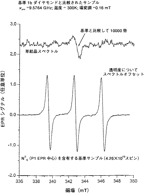
vii)カットされたCVD合成石(1a)のEPRスペクトルは、室温でBrukerX−バンド(9.5GHz)分光計を用いて記録された。単一の置換窒素は0.014ppmの検出限界で検出することができなかった(P1 EPR中心)。高い出力で、1.6x1015cm-3のスピン密度上に上限を設定してg=2.0028に近い弱い広い線が観察できた(図5)。
【0076】
例 2
条件に以下の変更を用いて、例1に示す方法が繰り返された:
2つの基体が例1において記載されたとおりの低い基体欠陥のための方法を用いて造られた。カットされたCVD合成石のための基体(2a)は、すべての面{100}で、6.8mmx6.65mmx0.71mm厚さであった。また、光学プレートの製造のために、追加の同様な基体(2b)が用いられた。
【0077】
酸素エッチングは30分間780℃及び7.8kWの正味出力においてであった。
水素エッチングは30分間795℃においてであった。
成長は、840℃の温度で、加えられた32sccm CH4を用いて起こった。
成長中の雰囲気は、<100ppbのN2を含有した。
【0078】
成長の完了の際、基体(2a)からのCVD層は、2.75mmの厚さであった。この層は慣用の宝石原石加工技術を用いて、実験の目的のために丸いブリリアントカット宝石の原石の形での、カットされたCVD合成体として加工された。最終カットされたCVD合成石は0.3カラットの重さを有し、そして標準のダイヤモンド等級化システムを用いてE及びVS1に等しい色及び品質の等級を有した。
【0079】
カットされた合成石(2a)及び光学プレート(2b)は、以下に提供された且つ添付図面において提供されたデータによりさらに特徴づけられた。
(i)プレート(2b)の収集距離は>400μmであると測定された。
(ii)50V/μmの印加電場でのプレート(2b)の抵抗率は、1x1014Ωcmを超えた。
【0080】
(iii)514nmでのアルゴンイオンレーザー光を用いて励起された、77KでのカットされたCVD合成石(2a)のラマン/光ルミネセンススペクトルは、ラマン線により支配された(図6)。575nmでのゼロ−フォノン線は弱かった、そしてそのピーク強度の、ラマンピーク強度に対する比は約1:28であった。ラマン線幅(FWHM)は1.54cm-1であった(図7)。
【0081】
(iv)カットされたCVD合成石(2a)の77Kで記録されたCLスペクトルは235nmでの極度に強い自由励起子放出により支配された(図8)。
(v)光学プレート(2b)の光学吸収スペクトルは本来的でない(外来の)吸光特徴を示さなかった、そして測定された吸光度はダイヤモンドについて予測された反射損失によってのみ限定された(図9)。
【0082】
(vi)カットされたCVD合成石(2a)のEPRスペクトルは、室温で、Bruker X−バンド(9.5GHz)分光計を用いて記録された。単一置換窒素は、0.014ppmの検出限界で、検出されることができなかった(P1 EPR中心)。高い出力で、1.6x1015cm-3のスピン密度上に上限を置いて、g=2.0028に近い弱い広い線を観察することができた(図10)。
【0083】
例 3
高温/高圧合成タイプ1bダイヤモンドは高圧力プレス中で成長し、そして低いサブ表面損傷を有する研磨されたプレートを形成するために例1において記載された方法を用いて造られた。この段階での表面粗度は、1nm未満のRAであった。その基体は、ダイヤモンドのために適当な高温ろうづけを用いてタングステン基体上に載せられた。これを反応器中に導入し、上に記載されたとおりにして成長サイクルを開始し、そしてさらに特定的には:
【0084】
1)反応器は使用精製装置の点と予め適合化されており、上に記載された修正GC法により測定されたときに80ppb以下までに、入ってくるガス流中の窒素水準を減少させた。
2)333x102Paの圧力で、O2/Ar/H2の15/75/600のsccmを用いて酸素エッチングとしてプラズマ処理を開始した。これに続いて、75/600sccmのAr/H2を用いて、Hエッチングを行った。この場合に30sccmで流動するCH4である炭素源の添加により、成長を開始した。この段階での成長温度は780℃であった。
【0085】
3)成長が行われた雰囲気は、上に記載された修正GC法により測定されたとき、100ppb未満の窒素を含有した。
4)成長期間の完了の際、反応器から基体を取り出し、そして3.2mm厚さのCVDダイヤモンド層を基体から取り出した。
【0086】
5)上に記載されたとおりの、ヘクト(Hecht)関係を用いて300Kで測定されたμτ積は電子について3.3x10⁻³cm2/Vであり、そして正孔について1.4x10-3cm2/Vであり、約2.3x10-3cm2/Vの平均μτ積であった。
6)空間電荷制限時間の飛行(flight)実験は、300Kのサンプル温度で電子移動度μeを4000cm2/Vsであると測定した。
【0087】
7)空間電荷制限時間の飛行(flight)実験は、300Kのサンプル温度で正孔移動度μhを3800cm2/Vsであると測定した。
8)SIMS測定は、(H及びその同位体を除いて)5x1016cm-3以上の濃度で存在する単一種不純物を何ら示していない。
【0088】
測定された抵抗率は300Kで測定されたとき、50V/μmの印加電圧で2x1013Ωcmを超えていた。破壊電圧は100V/μmを超えた。
【0089】
例 4
追加のダイヤモンド層を生成するために、例3に示す方法が繰り返された。(300Kで得られた)この層及び例1〜3の層の種々の性質が下記表において示される:
【0090】
【図面の簡単な説明】
【図1】514nmのアルゴンイオンレーザー励起を用いて77Kで記録された、カットされたCVD合成石(1a)のラマン/光ルミネセンススペクトル。
【図2】1.52cm-1のラマン線幅(FWHM)を示す、カットされたCVD合成石(1a)の室温ラマンスペクトル(514nmアルゴンイオンレーザー励起)である。
【図3】強い235nm自由励起子放出を示す、カットされたCVD合成石(1a)上の2つの位置からの77Kで記録された陰極ルミネセンススペクトル。
【図4】光学プレート(1b)のUV吸収スペクトル。
【図5】高い出力で観察することができた、P1の不存在、そしてg=2.0028に近い弱い広い線を示す、カットされたCVD合成石(1a)について室温で得られたX−バンド(9.5GHz)EPRスペクトル。サンプルについてのプロットの尺度は基準サンプルの尺度より10000倍大きいことに留意されたい。
【図6】514nmアルゴンイオンレーザー励起を用いて、77Kで記録された、カットされたCVD合成石(2a)のラマン/光ルミネセンススペクトル。
【図7】1.54cm-1のラマン線幅(FWHM)を示す、カットされたCVD合成石(2a)の室温ラマンスペクトル(514nmアルゴンイオンレーザー励起)。
【図8】カットされたCVD合成石(2a)から77Kで記録されたCL自由励起子放出スペクトル。
【図9】光学プレート(2b)のUV/可視光線吸収スペクトルである。
【図10】高い出力で観察することができた、P1の不存在、及びg=2.0028に近い弱い広い線を示す、室温で得られたカットされたCVD合成石(2a)のBruker X−バンド(9.5GHz)EPRスペクトル。サンプルについてのプロットの尺度は基準サンプルの尺度より10000倍大きいことに留意されたい。[0001]
Background of the Invention
The present invention relates to diamond, and more particularly to diamond produced by chemical vapor deposition (hereinafter referred to as CVD).
[0002]
Methods for depositing diamond-like materials on a substrate by CVD are well established today and have been widely described in patents and other literature. When diamond is deposited on a substrate, the process generally involves halogen (eg F, Cl) and C or carbon containing radicals and other reactive species such as CH in the form of hydrogen or atoms upon dissociation.x, CFx(Provided that x can be from 1 to 4). There can also be an oxygen-containing source as well as a source for nitrogen and for boron. In many methods, an inert gas such as helium, neon or argon is also present. Thus, a typical source gas mixture is a hydrocarbon CxHy(Wherein x and y can each be 1 to 10), or halogenated hydrocarbon CxHyHalz(Where Hal = halogen, x and z can each be 1-10 and y can be 0-10) and optionally contain one or more of the following: Wa: COx(Where x can be between 0.5 and 2), O2, H2, N2, NHThree, B2H6And inert gas. Each gas can exist in its natural isotope ratio, or the relative isotope ratio can be artificially controlled; for example, hydrogen can exist as deuterium or tritium, And carbon12C or13Can exist as C. Dissociation of the source gas mixture can be effected by an energy source such as microwave, RF energy, flame, hot filament, or by a jet-based technique, and the reactive gas species so generated is the substrate Deposited on top and forms a diamond.
[0003]
CVD diamond can be produced on a variety of substrates. Depending on the type of substrate and the details of the processing chemistry, polycrystalline or monocrystalline CVD diamond can be produced. The production of homoepitaxial CVD diamond layers has been reported in the literature. The prior art has generally involved itself in the thermal, optical and mechanical properties of CVD diamond.
[0004]
Summary of the Invention
According to a first aspect of the present invention, there is provided a layer of high quality single crystal CVD diamond having a thickness of at least 2 mm, preferably greater than 2.5 mm, and more preferably greater than 3 mm. The
[0005]
The high quality diamond can be characterized by one or more of the following. These properties are observable in the bulk volume of the layer or stone and in the {100} growth sector if present and recognizable:
[0006]
1) High charge collection distance of at least 100 μm, preferably at least 150 μm, more preferably at least 400 μm. All collection distances are measured with an applied electric field of 1 V / μm and 300 K (ie 20 ° C., considered equivalent for the purposes of this invention). In high quality type IIa natural diamond, the charge collection distance is reported to be substantially less than 100 μm, more typically about 40 μm, with an applied electric field of 1 V / μm.
[0007]
2) Assuming all measurements are made at 300K, 1.0x10⁻⁶cm2/ V, preferably 1.5 × 10⁻⁶cm2/ V, more preferably 4 × 10⁻⁶cm2High value for the product of average carrier mobility and lifetime μτ, such as> / V.
[0008]
3) 10% at an applied electric field of 50 V / μm in the off state.12Greater than Ωcm, preferably 2 × 10¹³Greater than Ωcm, more preferably 5 × 10¹⁴Resistance measured at 300K, greater than Ωcm.
[0009]
In devices with wide band gaps (band gaps), such as devices made from diamond, the number of free charge carriers present under equilibrium conditions is extremely low and is governed by lattice defects and incentives from impurities. Such a device is said to be in the “off state”. The device is loaded with charge carriers by means such as optical excitation (primarily using optical energy close to or greater than the width of the forbidden band) or by charged particle excitation (eg alpha or beta particles) Excited can enter “on state”. In the on state, the free carrier density exceeds the equilibrium level and the device returns to the off state when the source of excitation is removed.
[0010]
4) 2400cm2V-1s-1Larger, preferably 3000cm2V-1s-1Larger, more preferably 4000 cm2V-1s-1Larger electron mobility measured at 300K (μe). In high quality type IIa natural diamond, the electron mobility is 300K, typically 1800cm2V-1s-1The exceptional value reported is 2200 cm.2V-1s-1Up to.
[0011]
5) 2100cm2V-1s-1Larger, preferably 2500 cm2V-1s-1Larger, more preferably 3000 cm2V-1s-1Larger hole mobility measured at 300K (μh). In high quality type IIa natural diamond, the hole mobility is typically 300K and 1200cm.2V-1s-1The exceptional value reported is 1900 cm2V-1s-1Up to.
[0012]
It will be appreciated from the above description that the diamond of the present invention has electronic properties that are much superior to those present in natural high quality diamond. This is surprising and diamond with properties that are useful, for example, for electronic applications where a thick layer is needed and for the economic production of thinner layers, for other electronic devices I will provide a. Because of the reduced cost in terms of substrate and synthetic manufacturing, there is an advantage in synthesizing one thick layer and processing it into multiple thin layers.
[0013]
The diamonds of the present invention are also diamonds in high pressure experiments and production that allow the diamond's low defect density to make it much stronger than natural diamond and to operate under more severe conditions of temperature and pressure. Suitable for use as anvil.
[0014]
The diamond of the present invention has a suitable thickness, for example, to allow it to be cut and produce one or more gemstones from the diamond.
[0015]
In addition to the properties described above, the diamond layer of the present invention can have one or more of the following properties:
[0016]
1) Level of any one impurity of 5 ppm or less, and total impurity content of 10 ppm or less. Preferably, the level of any impurity is 0.5 ppm or less to 1 ppm, and the total impurity content is 2 ppm or less to 5 ppm. The concentration of impurities is determined by secondary ion mass spectrometry (SIMS), glow discharge mass spectrometry (GDMS), or combustion mass spectrometry (CMS), electron paramagnetic resonance (EPR) and IR (infrared) absorption, and further Single substituted nitrogen can be measured by optical absorption measurements at 270 nm (calibrated against a standard value obtained from a sample analyzed degradatively by combustion analysis). In the above description, “impurities” exclude hydrogen and its isotopic forms.
[0017]
2) Low or absent 575 nm cathodoluminescence (CL) line and associated photoluminescence (PL) measured at 77K under 514 nm Ar ion laser excitation (nominal 300 mW incident beam), Is 1332cm-1The diamond Raman peak at <1/25 has a peak height, preferably <1/300 peak height, more preferably <1/1000 peak height. These bands are associated with nitrogen / vacancy defects and their presence indicates the presence of nitrogen in the film. Due to the possible presence of competing quenching mechanisms, the normalized intensity of the 575 nm line is not a quantitative measure of nitrogen, and also its absence is a clear indication of the absence of nitrogen in the film not. CL is the luminescence resulting from excitation by an electron beam with a typical beam energy of 10-40 keV that transmits about 10 microns into the sample surface. Photoluminescence is more generally excited across the sample volume.
[0018]
3) (i) Strong free exciton (FE) emission in the cathodoluminescence spectrum collected at 77K.
Free exciton emission disappears due to structural defects such as point defects and dislocations. The presence of strong free exciton emission in the cathodoluminescence spectrum indicates a substantial absence of dislocations and impurities. The link between low defect and impurity density and high FE emission intensity has been previously reported for each crystal in polycrystalline CVD diamond synthesis.
[0019]
(Ii) Strong free exciton emission in the room temperature UV-excited (ultraviolet excited) photoluminescence spectrum.
Free exciton emission can also be excited by radiation above the bandgap width, for example by 193 nm radiation from an ArF excimer laser. The presence of strong free exciton emission in the photoluminescence spectrum excited in this way indicates the substantial absence of dislocations and impurities. The intensity of free exciton emission excited by a 193 nm ArF excimer laser at room temperature is such that the quantum yield for free exciton emission is at least 10-FiveThe strength is as follows.
[0020]
4) Monosubstituted nitrogen centers [NC] at concentrations of <100 ppb, typically <40 ppb, more typically <20 ppb, indicating low levels of nitrogen in electron paramagnetic resonance (EPR)O.
[0021]
5) In EPR, g = 2.0028, <1 × 1017cm-3Spin density, more typically <5 × 1016cm-3Spin density. In single crystal diamonds, this line is related to the lattice defect concentration and is typically large in natural type IIa diamonds, in CVD diamond plastically deformed by depressions, and in low quality homoepitaxial diamonds.
[0022]
6) has UV / visible and IR (infrared) transparency close to the theoretical maximum for diamond, more specifically, low or no mono-substituted nitrogen absorbance at 270 nm in UV light and IR 2500 to 3400cm-1Excellent optical properties with low or no C—H stretching absorption in the spectral range of.
[0023]
The properties described above could be observed in most volumes of layers or stones. There may be portions of volume where certain properties cannot be observed, typically less than 10% by volume.
[0024]
According to another aspect, the present invention provides a synthetic diamond in the form of a gemstone made from a layer of the type described above.
[0025]
The novel thick single crystal CVD diamond layer of the present invention can be made by the method of forming yet another aspect of the present invention. This method provides a diamond substrate having a surface that is substantially free of crystal defects, provides a source gas, dissociates the source gas, and contains less than 300 parts per billion (300 ppb) nitrogen. Including homoepitaxial diamond growth on a low defect level surface in an atmosphere.
[0026]
In order to synthesize a thick layer on the substrate surface, it is important to achieve a substrate surface that is substantially free of surface defects such that such defects can cause dislocations and associated defects in the overgrown CVD layer. This is because, and once present, these dislocation structures cannot be easily terminated in the layer, but generally diversify and spread as the layer grows thick, resulting in strains, defects and cracks. This is because of this. Even at very low levels, the nitrogen in the process plays a role in governing the morphology of the growing surface, causing a rearranged and defective growth as the layer thickness increases. Results in growth.
[0027]
The present invention provides that at least one axis is present along the <100> crystal direction or along the main axis of symmetry of the stone, greater than 2 mm, preferably greater than 2.5 mm, more preferably greater than 3.0 mm. Further provided is a CVD diamond formed from a polished single crystal CVD layer as described above in the form of a gemstone characterized by having three large, orthogonal dimensions. The diamond is a high quality diamond and can have one or more of the properties identified above.
[0028]
Description of embodiment
The single crystal CVD diamond layer of the present invention has a thickness of at least 2 mm, is a high quality diamond layer, and is particularly a high crystal integrity and high purity diamond layer. This is clearly shown by diamond having one or more of the properties identified above.
[0029]
The collection distance can be determined by methods known in the art. The collection distance referred to in this specification was determined by the following method:
[0030]
1) An ohmic spot contact is placed on either side of the layer under test. This layer is typically about 300-700 μm thick and 5-10 square millimeters, allowing for 2-6 mm diameter spot contacts. The formation of ohmic contacts (rather than contacts exhibiting diode behavior) is important for reliable measurements. This can be accomplished in several ways, but typically the method is as follows:
i) Oxygen termination of the diamond surface using, for example, oxygen plasma ash to minimize surface electrical conductivity (reduce device “dark current”);
ii) First a carbide former (eg Ti, Cr), then a protective coating, typically a metal coating consisting of a thick layer of Au (to which a wire bond can be made) is sputtered, evaporated or similar It is deposited on the diamond by the method. The contact is then annealed typically at 400-600 ° C. for about 1 hour.
[0031]
2) Wire bonding to the contacts is performed, typically using a bias voltage of 2-10 kV / cm, and the diamond is connected in the circuit. “Dark current” or leakage current is characterized and in good samples should be less than 5 nA at 2.5 kV / cm, more typically less than 100 pA.
[0032]
3) Collecting distance measurement
a) indicates that an event has occurred, and
b) To ensure that the beta particles are not stopped in the diamond film, resulting in the formation of a much larger number of charge carriers, use a Si trigger detector on the exit surface to Done by exposure to beta radiation. The signal from the diamond is then read by a high gain charge amplifier and based on a known rate of formation of charge carriers of about 36 electron / hole pairs per linear μm passed by the beta particles and collected. The distance can be calculated from the measured charge according to the following equation:
CCD = CCE x t
(Where t = sample thickness,
CCE = charge collection efficiency = collected charge / total charge generated,
CCD = charge collection distance)
[0033]
Obviously, the measured charge collection distance is limited to the thickness of the sample;
This is represented by the Hecht relationship provided later.
[0034]
4) To complete, the collection distance is measured over a range of values of applied bias voltage both before and after, and the characteristic collection distance is fully functional for bias voltages up to 10 kV / cm bias Only for samples exhibiting a linear behavior with a bias voltage of 10 kV / cm. Also, the overall measurement method is repeated several times to ensure the repeatability of the behavior, since the values measured for the poorer samples may decline with time and processing history.
[0035]
5) Another problem in measuring the collection distance is whether the material is pumped or not pumped. “Pumping” a material (also called “priming”) can increase the measured collection distance typically by a factor of 1.6 (although this can vary) in polycrystalline CVD diamond In some cases, the material consists of exposing it to certain types of radiation (beta rays, gamma rays, etc.) for a sufficient period of time. The effect of priming is generally low in highly pure single crystal diamonds: priming with a factor of 1.05-1.2 is in common with unmeasurable priming in some samples. De-pumping can be achieved by exposure to sufficiently intense white light or light of a selected wavelength, and the process is believed to be completely reversible. The collection distances referred to in this specification are all unpumped whatever the final application of the material. In certain applications (eg high energy particle physics experiments), the increase in collection distance associated with pumping can be advantageously used to increase the detectability of individual events by shielding the detector from any de-pumping radiation. Can do. In other applications, instability in device gain (gain) associated with pumping is very detrimental.
[0036]
The single crystal CVD diamond of the present invention, in one form of the present invention, has a high resistivity in the off state, with a high applied electric field, and more specifically applied at 50 V / μm as measured at 300 K 1x10 in electric field12Over Ωcm, preferably 2 × 10¹³More than Ωcm, more preferably 5 × 10¹⁴Resistivity R exceeding Ωcm1Have Such a resistivity at such a high applied electric field indicates the purity of the diamond and indicates the substantial absence of impurities and defects. Low purity or low crystal integrity materials can exhibit high resistivity at low applied electric fields, for example <30 V / μm, but rise rapidly with applied electric fields greater than 30 V / μm and generally 45 V / μm Shows dielectric breakdown behavior along with leakage current. Resistivity can be determined from leakage (dark) current measurements by methods known in the art. The sample under test is made as a plate of uniform thickness, to accept suitable contacts (evaporated, sputtered or doped diamond) whose external connection can be made to the voltage supply , Cleaned using standard diamond cleaning techniques, and then partially or wholly encapsulated to minimize the risk of flashover (burst discharge). It is important to ensure that the encapsulation does not add significantly to the measured leakage current. Typical sample dimensions are 0.01 to 0.5 mm thick and 3 × 3 mm to 50 × 50 mm in the lateral direction, but smaller or larger dimensions can be used.
[0037]
The single crystal CVD diamond of the present invention is 1.0 × 10⁻⁶cm2Μτ product greater than / V, preferably 1.5 × 10⁻⁶cm2Μτ product greater than / V, more preferably 4.0 × 10⁻⁶cm2It can have a μτ product greater than / V. The μτ product is related to the charge collection distance using the following equation:
μτE = CCD
(Cm2/ Vs) x (s) x (V / cm) = cm
(However, E = applied electric field)
[0038]
In its particularly preferred form, the single crystal CVD diamond of the present invention has a high μτ product that translates to a high charge collection distance.
[0039]
When an electric field is applied to a sample using an electrode, it is possible to separate electron-hole pairs generated by photon irradiation of the sample. Holes are carried towards the cathode and electrons are carried towards the anode. Light with a short wavelength (UV light) and photon energy above the band gap of diamond have a very small penetration depth into diamond, and by using this type of light, only one type of carrier It is possible to confirm the contribution of that type of carrier on which the electrode is illuminated.
[0040]
The μτ product referred to in this specification is measured in the following manner:
![]()
(Ii) Translucent contacts are sputtered on both sides of the diamond plate and then patterned using standard photolithography techniques. This process forms a suitable contact.
[0041]
(Iii) 10 μs pulse of monochromatic Xe light (wavelength 218 nm) is used to excite the carrier, and the generated photocurrent is measured in an external circuit. A pulse length of 10 μs is much longer than other processes such as transit time and carrier lifetime, and the system is considered to be balanced at all times during the pulse. The penetration of light into diamond at this wavelength is only a few microns. The total number of electron-hole pairs generated by the light pulse is relatively low, and at that time, the relatively low light intensity (approximately .0. 1W / cm2) Is used. The applied electric field is maintained below a certain threshold, but the mobility becomes electric field dependent above that threshold. The applied electric field is also maintained below a certain value, but above that value, a significant percentage of charge carriers reach the far side of the diamond and the total charge collected shows saturation (contact In the blocked state; non-blocking contacts can show gain in terms of this value).
[0042]
(Iv) The μτ product is derived by relating the collected charge to the applied voltage using the following Hecht relationship:
Q = NoeμτE / D [1-exp {−D / (μτE)}]
In this equation, Q is the charge collected with the unilluminated contact and NoIs the total number of electron-hole pairs generated by the light pulse, E is the applied electric field, D is the thickness of the sample, and μτ is the product of mobility and lifetime to be determined.
[0043]
(V) As an example, if the illuminated electrode is an anode (cathode) then charge carriers are generated within a few μm of the surface and the charge transfer of electrons (holes) to the adjacent electrode Can be ignored. On the other hand, hole (electron) charge transfer to the opposing contact is significant, and both μ and τ are specific to specific charge carriers moving towards the unirradiated electrode. It is limited by the μτ product.
[0044]
The CVD diamond layer of the present invention can be applied to a diamond substrate (where the substrate is either synthetic diamond, natural diamond or CVD diamond). Advantages of this method include providing a larger overall thickness, the thickness of which limits the application, or providing a support for the CVD layer whose thickness has been reduced by processing. Also, the CVD diamond layer of the present invention may form one layer in a multi-layer device, in which case the other diamond layer, for example to provide electrical contact or electronic connection to the diamond layer, It may be doped or simply present to provide a support for the diamond layer.
[0045]
It is important for the production of thick high quality single crystal CVD diamond layers that the growth be performed on a diamond surface that is substantially free of crystal defects. In this context, defects not only mean dislocations, other crystal defects and microcracks, but also any other breaks to double boundaries, point defects, low angle boundaries and crystal lattices. Is also included. Preferably, the substrate is a low birefringence type Ia or IIb natural diamond, Ib or IIa high pressure / high temperature synthetic diamond, or CVD synthetic single crystal diamond.
[0046]
The defect density is referred to as a plasma or chemical etch (revealing plasma etch) that has been optimized to reveal defects, for example using a brief plasma etch of the type described below. ) Is most easily characterized by optical evaluation. Two types of defects can appear:
[0047]
1) Defects inherent in the quality of the substrate material. In selected natural diamonds, the density of these defects is 50 / mm.2Can be as low as 10 more typical values2/ Mm2Whereas in other diamonds it is 106/ Mm2Or more.
[0048]
2) Defects resulting from polishing including dislocation structures and microcracks in the form of "chatter tracks" along the polishing line. The density of these defects can vary considerably across the sample, with a typical value of about 102/ Mm2To 10 in a poorly polished region or sampleFour/ Mm2It is in the range up to more.
[0049]
Thus, the preferred low defect density is that the density of surface etch features associated with defects is 5 × 10 5 as described above.Three/ Mm2Or less, more preferably 102/ Mm2It is as follows.
[0050]
Thus, the level of defects at and below the substrate surface where CVD growth takes place can be minimized by careful manufacture of the substrate. In this case, the production includes all processes applied to the material from the mine (in the case of natural diamonds) or from the synthesis (in the case of synthetic materials), which each step involves the substrate. This is because the defect density in the material may be affected by the plane on which the substrate surface is finally formed when the process for forming is completed. Specific processing steps include conventional diamond processing such as mechanical sawing, lapping and polishing conditioning, and less conventional techniques such as laser processing or ion implantation, and lift-off techniques, chemical / mechanical polishing, and It will include both liquid and plasma chemistry processing techniques. Surface RA(The arithmetic average of the absolute deviation value of the surface shape measured by the needle roughness preferably over a length of 0.08 mm) should be minimized, and a typical value before any plasma etching is a few nanometers That is, it is less than 10 nm.
[0051]
One particular way to minimize substrate surface damage is to include in-situ plasma etching on the surface where homoepitaxial diamond growth should occur on the surface. In principle, this etching need not be in situ and need not be immediately before the growth process, but in situ etching avoids all the risks of additional physical damage or chemical contamination, so If it is a field etch, the greatest advantage is achieved. In situ etching is also generally most convenient when the growth process is also plasma based. Plasma etching can use conditions similar to the deposition or diamond growth process, but provides good control of the etch rate in the absence of any carbon-containing source gas and generally at slightly lower temperatures. For example, it can consist of one or more of the following:
[0052]
(I) optionally a small amount of Ar and a small amount of O required2Together with oxygen etching using mainly hydrogen. Typical oxygen etching conditions are 50-450x10.2Pressure of Pa, 1-4% oxygen content, 0-30% argon content, etching gas with the remainder containing hydrogen (all percentages by volume), 600-1100 ° C. (more typically 800 C) substrate temperature and a typical duration of 3 to 60 minutes.
(Ii) Hydrogen etching similar to (i) but without oxygen present.
(Iii) Other methods for etching that are not solely based on argon, hydrogen and oxygen, such as etching methods using halogens, other inert gases or nitrogen, can be used.
[0053]
The etching typically consists of an oxygen etch followed by a hydrogen etch and then moves directly to synthesis by introduction of a carbon source gas. The etch time / temperature is chosen to allow any remaining surface damage from the process to be removed and to allow contaminants to be removed for all surfaces, but not to form a highly rough surface. And is chosen so that it does not etch extensively along extended defects (such as dislocations) across the surface, thus creating deep holes. Since etching is aggressive, the design of the chamber and the selection of materials for its components are such that the plasma does not transfer the chamber material into the gas phase or to the substrate surface. Is especially important for. Hydrogen etching after oxygen etching is less specific for crystal defects, rounds the sharp corners caused by oxygen etching (which aggressively attacks such defects), and for subsequent growth Provides a smoother and better surface.
[0054]
The surface or surfaces of the diamond substrate on which CVD diamond growth occurs are preferably {100}, {110}, {113} or {111} surfaces. Due to processing constraints, the actual sample surface orientation may differ by up to 5 ° from these orientations, and in some cases up to 10 °, but this is reproducible. It is less preferred because it adversely affects
[0055]
It is also important in the method of the present invention that the impurity content of the environment in which the CVD growth is performed is appropriately controlled. More particularly, the diamond growth is substantially nitrogen-free atmosphere, ie less than 300 parts per billion (less than 300 ppb as a molecular fraction of the total gas volume), preferably 1 billion minutes Must be done in the presence of an atmosphere of less than 100 parts (less than 100 ppb). The role of nitrogen in the synthesis of CVD diamond, and specifically polycrystalline CVD diamond, has been reported in the literature. For example, a gas phase nitrogen level of 10 parts per million (10 ppm) or higher alters the relative growth rate between the {100} and {111} planes, with an overall increase in growth rate, and some It was shown in these reports that the quality changed in some cases. It was further suggested that for some CVD diamond synthesis methods, a low nitrogen content of a few parts per million or less (a few ppm or less) can be used. However, these reported methods ensure that the nitrogen content is substantially below 1 part per million (1 ppm or less) and in the region below 300 parts per billion (300 ppb). It does not disclose any method of nitrogen analysis that is sufficiently sensitive to do so. Measurement of these low values of nitrogen level requires high performance monitoring, such as monitoring that can be achieved by gas chromatography, for example. Now, an example of such a method is described below:
[0056]
(1) Standard Gas Chromatography (GC) technology consists of: A sample flow of gas is drawn from the point of interest using a narrow inner diameter sample pipe for maximum flow velocity and minimum dead volume (dead volume) Optimized and passed through the GC sampling coil before going to disposal. The GC sampling coil is fixed and has a known volume (typically 1 cm for standard pressure injection)Three), Which is transferred from its position in the sample piping to the carrier gas (high purity He) piping and fed into the gas chromatography column. This places a sample of a known volume of gas in the gas stream entering the column: in the art, this method is called sample injection.
[0057]
The injected sample is carried by the carrier gas through the first GC column (filled with a molecular sieve optimized for the separation of simple inorganic gases) and is partially separated. High concentration primary gas (eg H2, Ar) causes column saturation, which makes complete separation of nitrogen difficult. The relevant part of the effluent from the first column is then transferred into the feed stream of the second column, thereby preventing the main amount of other gases from being sent into the second column and preventing column saturation. , And target gas (N2) Allows complete separation. This method is called “heart-cutting”.
[0058]
The output stream of the second column is placed in a discharge ionization detector (DID) that detects the increase in leakage current in the carrier gas caused by the presence of the sample. Chemical identity is determined by the gas residence time calibrated from a standard gas mixture. The response of the DID is linear over order magnitudes greater than 5, and is calibrated by use of a special calibrated gas mixture, typically in the range of 10-100 ppm, performed by gravimetric analysis, and then the supplier Is confirmed. The linearity of DID can be confirmed by careful dilution experiments.
[0059]
(2) This known technique of gas chromatography was further modified and developed for this application as follows: Here, the method to be analyzed is 70-500 × 102Typically operating at Pa. Normal GC operation uses an excess pressure above the atmospheric pressure of the source gas to drive the gas through the sample piping. Here, the sample is moved by installing a vacuum pump at the waste end of the piping and the sample is drawn below atmospheric pressure. However, piping obstructions can cause significant pressure drops in the piping while gas is flowing, affecting calibration and sensitivity. Therefore, a valve is placed between the sample coil and the vacuum pump, this valve to stabilize the pressure at the sample coil and to be able to measure with a pressure gauge Closed for a short period before sample injection. The sample coil capacity is approximately 5 cm to ensure that a sufficient mass of sample gas is injected.ThreeWill be increased. Depending on the design of the sample piping, this technique is about 70x102It is possible to operate by effectively reducing the pressure of Pa. The calibration of the GC depends on the mass of the sample being injected, and the greatest accuracy is obtained by calibrating the GC using the same sample pressure that can be obtained from the source under analysis. The very high standard vacuum and gas handling practices must be observed to ensure that the measurements are correct.
[0060]
The point of sampling is upstream of the synthesis chamber to characterize the incoming gas, indoor to characterize the room environment, or downstream of the chamber to measure the worst case value of nitrogen concentration in the room. , Can be.
[0061]
The source gas can be any known in the art and will contain a carbon-containing material that dissociates to produce radicals or any other reactive species. The gas mixture will also generally contain gases that are suitable for providing hydrogen or atomic forms of halogen.
[0062]
The dissociation of the gas source is preferably performed using microwave energy in a reactor that can be any known in the art. However, the transfer of all impurities from the reactor should be minimal. Microwave systems can be used to ensure that the plasma is placed away from all surfaces except the substrate surface and its mount (mount) where diamond growth can occur. Examples of preferred base materials are molybdenum, tungsten, silicon and silicon carbide. Examples of preferred reactor chamber materials are stainless steel, aluminum, copper, gold and platinum.
[0063]
High microwave power (typically 3-60 kW for 50-150 mm substrate diameter) and high gas pressure (50-500 × 10 62Pa, preferably 100 to 450 × 102A high plasma power density resulting from Pa) should be used.
[0064]
Using the preferred conditions described above to produce high quality single crystal CVD diamond layers> 2 mm thick (eg 3.4 mm thick) and gems with three orthogonal dimensions greater than 2 mm It was possible to produce high quality CVD synthetic cut stones from these layers in the form of rough stones (eg 0.31 carat, 2.6 mm height, 4.3 mm girdle diameter round brilliant cut).
[0065]
Now, examples of the present invention are described below:
Example 1
A suitable substrate for synthesizing the CVD diamond layer of the present invention can be made as follows:
i) The selection of stone materials (Ia natural stone and Ib HPHT stone) was optimized based on microscopic studies and birefringence images to identify substrates free of strain and defects.
ii) Laser sawing, lapping, and polishing processes are used to minimize substrate defects, using a method of revealing plasma etching to examine the defect levels introduced by the process. It was.
[0066]
iii) The density of defects that can be measured after the manifestation etch is largely dependent on the quality of the material and 5 × 10Three/ Mm2Hereinafter, generally 102/ Mm2It was quite possible to produce substrates that were: The substrate made by this method is then used for subsequent synthesis.
[0067]
High temperature / high pressure synthetic Ib diamond was grown in a high pressure press and made as a plate using the method described above to minimize substrate defects. The final plate was 5.8 mm x 4.9 mm x 1.6 mm thick with all faces {100}. The surface roughness at this point is R less than 1 nm.AMet. This substrate (substrate 1a) was mounted on a tungsten substrate using a suitable high temperature braze for diamond together with a second substrate (substrate 1b) that was similarly constructed. This is introduced into the reactor and the etching and growth cycles are started as described above, and specifically:
[0068]
1) The reactor was pre-adapted with respect to the purification equipment used and reduced the nitrogen level in the incoming gas stream to below 80 ppb as measured by the modified GC method described above.
2) 237x102At a substrate temperature of Pa and 849 ° C., O2/ Ar / H2In-situ oxygen plasma etching was performed using a 30/150/1200 sccm (standard cubic centimeter per second).
3) This can be achieved from the gas stream without interruption.2At the same time, hydrogen etching was performed at 830 ° C.
[0069]
4) This shifted to a growth process by adding a carbon source (in this case CH at 30 sccm)Four). At this stage, the growth temperature was 822 ° C.
5) The atmosphere in which the growth took place contained less than 100 ppb nitrogen as measured by the modified GC method described above.
[0070]
6) Upon completion of the growth period, the two substrates were removed from the reactor. The 3.4 mm thick CVD layer was removed from the substrate (1a) and cut using a standard gemstone manufacturing technique, in the form of a round brilliant cut gemstone for experimental purposes. Built as a body. This cut synthetic stone had a height of 2.62 mm (from table to culet) and a weight of 0.31 carat. The CVD layer from the substrate (1b) was used to make a CVD plate for the characterization of these elements, which is difficult to do quantitatively with round brilliant cuts.
[0071]
7) Next, the CVD synthesized layers are provided below and obtain the following data provided in the accompanying drawings FIGS. 1-5 (the CVD layers are referred to by the reference number of the substrate on which they were grown): Further characterized by:
i) The collection distance of the plate (1b) was measured to be> 400 μm.
ii) With an applied electric field of 50 V / μm, the resistance of the plate (1b) is 1 × 10¹⁴It exceeded Ωcm.
[0072]
iii) The Raman / photoluminescence spectrum of the cut CVD synthetic stone (1a) at 77K excited with argon ion laser light at 514 nm was dominated by the Raman line (FIG. 1). The zero-phonon line at 575 nm was extremely weak and the ratio of its peak intensity to the Raman peak intensity was about 1: 7800.
[0073]
iv) 1332 cm for cut CVD synthetic stone (1a)-1The Raman FWHM linewidth of the diamond wire at 1.52 cm (measured using 514 nm laser excitation)-1(FIG. 2).
v) The CL spectrum recorded at 77 K for the cut CVD synthetic stone (1a) was dominated by extremely strong free exciton emission at 235 nm (FIG. 3).
[0074]
vi) The optical absorption spectrum of the optical plate (1b) showed no intrinsic (foreign) absorption characteristics, and the absorbance measured at 240 nm was limited only by the expected reflection loss for diamond (FIG. 4). ).
[0075]
vii) The EPR spectrum of the cut CVD synthetic stone (1a) was recorded using a Bruker X-band (9.5 GHz) spectrometer at room temperature. No single substituted nitrogen could be detected with a detection limit of 0.014 ppm (P1 EPR center). 1.6x10 at high power15cm-3A weak broad line close to g = 2.0028 was observed with an upper limit set on the spin density (FIG. 5).
[0076]
Example 2
The method shown in Example 1 was repeated using the following changes in conditions:
Two substrates were made using the method for low substrate defects as described in Example 1. The substrate (2a) for the cut CVD synthetic stone was 6.8 mm × 6.65 mm × 0.71 mm thick on all sides {100}. An additional similar substrate (2b) was also used for the production of the optical plate.
[0077]
The oxygen etch was at 780 ° C. and 7.8 kW net power for 30 minutes.
Hydrogen etching was at 795 ° C. for 30 minutes.
Growth was performed at a temperature of 840 ° C. with 32 sccm CH added.FourHappened with.
Growth atmosphere is <100 ppb N2Contained.
[0078]
Upon completion of the growth, the CVD layer from the substrate (2a) was 2.75 mm thick. This layer was processed as a cut CVD composite in the form of a round brilliant cut gemstone for experimental purposes using conventional gemstone processing techniques. The final cut CVD synthetic weighed 0.3 carat and had a color and quality rating equal to E and VS1 using a standard diamond grading system.
[0079]
The cut synthetic stone (2a) and the optical plate (2b) were further characterized by the data provided below and in the accompanying drawings.
(I) The collection distance of the plate (2b) was measured to be> 400 μm.
(Ii) The resistivity of the plate (2b) at an applied electric field of 50 V / μm is 1 × 10¹⁴It exceeded Ωcm.
[0080]
(Iii) The Raman / photoluminescence spectrum of the cut CVD synthetic stone (2a) at 77K excited with argon ion laser light at 514 nm was dominated by the Raman line (FIG. 6). The zero-phonon line at 575 nm was weak and the ratio of its peak intensity to the Raman peak intensity was about 1:28. Raman line width (FWHM) is 1.54cm-1(FIG. 7).
[0081]
(Iv) The CL spectrum recorded at 77 K of the cut CVD synthetic stone (2a) was dominated by extremely strong free exciton emission at 235 nm (FIG. 8).
(V) The optical absorption spectrum of the optical plate (2b) showed no intrinsic (foreign) absorbance characteristics, and the measured absorbance was limited only by the expected reflection loss for diamond (FIG. 9).
[0082]
(Vi) The EPR spectrum of the cut CVD synthetic stone (2a) was recorded using a Bruker X-band (9.5 GHz) spectrometer at room temperature. No single substituted nitrogen could be detected with a detection limit of 0.014 ppm (P1 EPR center). 1.6x10 at high power15cm-3A weak broad line close to g = 2.0028 was observed with an upper limit on the spin density (FIG. 10).
[0083]
Example 3
High temperature / high pressure synthetic type 1b diamond was grown in a high pressure press and made using the method described in Example 1 to form a polished plate with low subsurface damage. The surface roughness at this stage is less than 1 nm RAMet. The substrate was mounted on a tungsten substrate using high temperature brazing appropriate for diamond. This is introduced into the reactor, starting the growth cycle as described above, and more specifically:
[0084]
1) The reactor was pre-adapted to the purification equipment used and reduced the nitrogen level in the incoming gas stream by up to 80 ppb or less as measured by the modified GC method described above. .
2) 333x102O at Pa pressure2/ Ar / H2The plasma treatment was started as oxygen etching using 15/75/600 sccm. This is followed by 75/600 sccm Ar / H2Then, H etching was performed. In this case, CH flowing at 30 sccmFourGrowth was started by adding a carbon source. The growth temperature at this stage was 780 ° C.
[0085]
3) The atmosphere in which the growth took place contained less than 100 ppb nitrogen as measured by the modified GC method described above.
4) Upon completion of the growth period, the substrate was removed from the reactor and a 3.2 mm thick CVD diamond layer was removed from the substrate.
[0086]
5) The μτ product measured at 300 K using the Hecht relationship as described above is 3.3 × 10 3 for electrons.-3cm2/ V and 1.4 × 10 6 for holes-3cm2/ V, about 2.3 × 10⁻³cm2The average μτ product of / V.
6) Space charge limited time flight experiment is performed with an electron mobility μ at a sample temperature of 300K.e4000cm2/ Vs.
[0087]
7) Space charge limited time flight experiment is performed with a hole mobility μ at a sample temperature of 300K.h3800cm2/ Vs.
8) SIMS measurements are 5x10 (excluding H and its isotopes)16cm-3It does not show any single species impurities present at these concentrations.
[0088]
The measured resistivity is 2 × 10 at an applied voltage of 50 V / μm when measured at 300K.13It exceeded Ωcm. The breakdown voltage exceeded 100 V / μm.
[0089]
Example 4
The method shown in Example 3 was repeated to produce additional diamond layers. Various properties of this layer (obtained at 300K) and the layers of Examples 1-3 are shown in the table below:
[0090]
[Brief description of the drawings]
FIG. 1 Raman / photoluminescence spectrum of a cut CVD synthetic stone (1a) recorded at 77 K using 514 nm argon ion laser excitation.
FIG. 2 1.52 cm-1It is the room temperature Raman spectrum (514 nm argon ion laser excitation) of the cut CVD synthetic stone (1a) which shows the Raman line width (FWHM).
FIG. 3 is a cathodoluminescence spectrum recorded at 77K from two positions on a cut CVD synthetic stone (1a) showing strong 235 nm free exciton emission.
FIG. 4 is a UV absorption spectrum of the optical plate (1b).
FIG. 5: X-rays obtained at room temperature for a cut CVD synthetic stone (1a) that can be observed at high power, showing the absence of P1, and a weak broad line close to g = 2.0028. Band (9.5 GHz) EPR spectrum. Note that the plot scale for the sample is 10,000 times greater than the scale for the reference sample.
FIG. 6 Raman / photoluminescence spectrum of cut CVD synthetic stone (2a) recorded at 77 K using 514 nm argon ion laser excitation.
FIG. 7 1.54 cm-1Room temperature Raman spectrum of a cut CVD synthetic stone (2a) showing the Raman line width (FWHM) of (514 nm argon ion laser excitation).
FIG. 8 CL free exciton emission spectrum recorded at 77K from a cut CVD synthetic stone (2a).
FIG. 9 is a UV / visible absorption spectrum of the optical plate (2b).
FIG. 10: Bruker X of cut CVD synthetic stone (2a) obtained at room temperature, showing the absence of P1 and a weak broad line close to g = 2.0028 that could be observed at high power -Band (9.5 GHz) EPR spectrum. Note that the plot scale for the sample is 10,000 times greater than the scale for the reference sample.
Claims (36)
1)1V/μmの印加電場で測定された、300Kで少なくとも100μmの高い電荷収集距離;
2)300Kで1.0x10 -6 cm 2 /Vを超えるような、平均キャリヤー移動度及び寿命μτの積についての高い値;
3)300Kで測定された、2400cm 2 V -1 s -1 より大きな電子移動度(μ e );
4)300Kで測定された、2100cm 2 V -1 s -1 より大きな正孔移動度(μ h );
5)オフ状態において、50V/μmの印加電場で300Kで10 12 Ωcmより大きな抵抗率。 A layer of high quality single crystal CVD diamond having a thickness of at least 2 mm and one or more of the following properties :
1) A high charge collection distance of at least 100 μm at 300 K measured with an applied electric field of 1 V / μm;
2) A high value for the product of average carrier mobility and lifetime μτ, such that it exceeds 1.0 × 10 −6 cm 2 / V at 300K ;
3) Electron mobility (μ e ) , measured at 300 K, greater than 2400 cm 2 V −1 s −1 ;
4) Hole mobility (μ h ) , measured at 300 K, greater than 2100 cm 2 V −1 s −1 ;
5) Resistivity greater than 10 12 Ωcm at 300K with an applied electric field of 50 V / μm in the off state .
Applications Claiming Priority (3)
| Application Number | Priority Date | Filing Date | Title |
|---|---|---|---|
| GB0014690A GB0014690D0 (en) | 2000-06-15 | 2000-06-15 | Diamond |
| GB0106929A GB0106929D0 (en) | 2001-03-20 | 2001-03-20 | Diamond |
| PCT/IB2001/001040 WO2001096634A1 (en) | 2000-06-15 | 2001-06-14 | Thick single crystal diamond layer method for making it and gemstones produced from the layer |
Publications (2)
| Publication Number | Publication Date |
|---|---|
| JP2004503461A JP2004503461A (en) | 2004-02-05 |
| JP4469552B2 true JP4469552B2 (en) | 2010-05-26 |
Family
ID=26244496
Family Applications (1)
| Application Number | Title | Priority Date | Filing Date |
|---|---|---|---|
| JP2002510742A Expired - Lifetime JP4469552B2 (en) | 2000-06-15 | 2001-06-14 | Thick single crystal diamond layer, method of making it and gemstone formed from that layer |
Country Status (16)
| Country | Link |
|---|---|
| US (3) | US7128974B2 (en) |
| EP (2) | EP1290251B8 (en) |
| JP (1) | JP4469552B2 (en) |
| KR (1) | KR100839707B1 (en) |
| CN (1) | CN1210445C (en) |
| AT (1) | ATE311486T1 (en) |
| AU (2) | AU2001266246B2 (en) |
| CA (1) | CA2412855C (en) |
| CZ (1) | CZ302229B6 (en) |
| DE (1) | DE60115435T2 (en) |
| ES (1) | ES2252244T3 (en) |
| GB (1) | GB2379451B (en) |
| IL (2) | IL153381A0 (en) |
| RU (1) | RU2287028C2 (en) |
| TW (1) | TWI250231B (en) |
| WO (1) | WO2001096634A1 (en) |
Families Citing this family (76)
| Publication number | Priority date | Publication date | Assignee | Title |
|---|---|---|---|---|
| US8591856B2 (en) | 1998-05-15 | 2013-11-26 | SCIO Diamond Technology Corporation | Single crystal diamond electrochemical electrode |
| US6582513B1 (en) | 1998-05-15 | 2003-06-24 | Apollo Diamond, Inc. | System and method for producing synthetic diamond |
| US6858080B2 (en) | 1998-05-15 | 2005-02-22 | Apollo Diamond, Inc. | Tunable CVD diamond structures |
| CZ302228B6 (en) * | 2000-06-15 | 2011-01-05 | Element Six (Pty) Ltd | Single crystal diamond layer prepared by chemical vapor deposition from gaseous phase |
| AU2001281404B2 (en) | 2001-08-08 | 2008-07-03 | Apollo Diamond, Inc. | System and method for producing synthetic diamond |
| DE10153310A1 (en) * | 2001-10-29 | 2003-05-22 | Infineon Technologies Ag | Photolithographic structuring process with a carbon hard mask layer produced by a plasma-assisted deposition process with diamond-like hardness |
| GB0130004D0 (en) * | 2001-12-14 | 2002-02-06 | Diamanx Products Ltd | Coloured diamond |
| GB0130005D0 (en) * | 2001-12-14 | 2002-02-06 | Diamanx Products Ltd | Boron doped diamond |
| GB0220772D0 (en) * | 2002-09-06 | 2002-10-16 | Diamanx Products Ltd | Coloured diamond |
| RU2328563C2 (en) * | 2002-09-06 | 2008-07-10 | Элемент Сикс Лимитед | Coloured diamonds |
| GB0220767D0 (en) * | 2002-09-06 | 2002-10-16 | Diamanx Products Ltd | Diamond radiation detector |
| GB0221949D0 (en) * | 2002-09-20 | 2002-10-30 | Diamanx Products Ltd | Single crystal diamond |
| GB0227261D0 (en) * | 2002-11-21 | 2002-12-31 | Element Six Ltd | Optical quality diamond material |
| FR2849867B1 (en) | 2003-01-10 | 2005-03-25 | Centre Nat Rech Scient | HIGH-SPEED DIAMOND GROWTH BY PLASMA MICROWAVE IN PULSE REGIME. |
| GB0303860D0 (en) * | 2003-02-19 | 2003-03-26 | Element Six Ltd | CVD diamond in wear applications |
| WO2005061400A1 (en) * | 2003-12-12 | 2005-07-07 | Element Six Limited | Method of incorporating a mark in cvd diamond |
| JP4697514B2 (en) * | 2004-01-16 | 2011-06-08 | 住友電気工業株式会社 | Diamond single crystal substrate manufacturing method and diamond single crystal substrate |
| US7481879B2 (en) | 2004-01-16 | 2009-01-27 | Sumitomo Electric Industries, Ltd. | Diamond single crystal substrate manufacturing method and diamond single crystal substrate |
| US7918293B1 (en) * | 2005-03-09 | 2011-04-05 | Us Synthetic Corporation | Method and system for perceiving a boundary between a first region and a second region of a superabrasive volume |
| JP5002982B2 (en) * | 2005-04-15 | 2012-08-15 | 住友電気工業株式会社 | Method for producing single crystal diamond |
| GB0508889D0 (en) * | 2005-04-29 | 2005-06-08 | Element Six Ltd | Diamond transistor and method of manufacture thereof |
| AU2006260656A1 (en) | 2005-06-22 | 2006-12-28 | Element Six Limited | High colour diamond layer |
| US9133566B2 (en) | 2005-12-09 | 2015-09-15 | Element Six Technologies Limited | High crystalline quality synthetic diamond |
| GB0622695D0 (en) | 2006-11-14 | 2006-12-27 | Element Six Ltd | Robust radiation detector comprising diamond |
| JP2010517263A (en) | 2007-01-22 | 2010-05-20 | エレメント シックス リミテッド | Diamond electronic devices and methods of manufacturing the same |
| JP5514552B2 (en) * | 2007-01-29 | 2014-06-04 | カーネギー インスチチューション オブ ワシントン | Novel laser applications of single crystal CVD diamond |
| JP5223201B2 (en) * | 2007-01-29 | 2013-06-26 | 日本電気株式会社 | Field effect transistor |
| JP5504565B2 (en) * | 2008-02-07 | 2014-05-28 | 独立行政法人物質・材料研究機構 | Diamond UV sensor element, manufacturing method thereof, and UV sensor device |
| WO2009114130A2 (en) * | 2008-03-13 | 2009-09-17 | Michigan State University | Process and apparatus for diamond synthesis |
| US20090260396A1 (en) * | 2008-04-16 | 2009-10-22 | Eitan Broukman | Methods for processing ornamental diamonds and corresponding ornamental diamonds |
| US8342164B2 (en) * | 2008-05-09 | 2013-01-01 | SCIO Diamond Technology Corporation | Gemstone production from CVD diamond plate |
| GB0813490D0 (en) | 2008-07-23 | 2008-08-27 | Element Six Ltd | Solid state material |
| GB0813491D0 (en) * | 2008-07-23 | 2008-08-27 | Element Six Ltd | Diamond Material |
| GB0819001D0 (en) | 2008-10-16 | 2008-11-26 | Diamond Detectors Ltd | Contacts on diamond |
| JP5891564B2 (en) * | 2009-06-26 | 2016-03-23 | エレメント シックス リミテッド | Method for producing fancy pale blue or fancy pale blue / green single crystal CVD diamond and the resulting product |
| US9255009B2 (en) | 2009-06-26 | 2016-02-09 | Element Six Technologies Limited | Diamond material |
| KR101130049B1 (en) * | 2009-09-08 | 2012-03-28 | 김일천 | Piston coated diamond like carbon thin film and Method of manufacturing the same |
| GB201000768D0 (en) * | 2010-01-18 | 2010-03-03 | Element Six Ltd | CVD single crystal diamond material |
| US9017633B2 (en) | 2010-01-18 | 2015-04-28 | Element Six Technologies Limited | CVD single crystal diamond material |
| US9023307B2 (en) * | 2010-05-17 | 2015-05-05 | Carnegie Institution Of Washington | Production of large, high purity single crystal CVD diamond |
| GB201013112D0 (en) * | 2010-08-04 | 2010-09-22 | Element Six Ltd | A diamond optical element |
| US9277792B2 (en) * | 2010-08-24 | 2016-03-08 | Board Of Trustees Of Michigan State University | Multicolored single crystal diamond gemstones and methods for forming the same |
| GB201015260D0 (en) | 2010-09-14 | 2010-10-27 | Element Six Ltd | A microfluidic cell and a spin resonance device for use therewith |
| GB201021985D0 (en) | 2010-12-24 | 2011-02-02 | Element Six Ltd | Dislocation engineering in single crystal synthetic diamond material |
| GB201104579D0 (en) * | 2011-03-18 | 2011-05-04 | Element Six Ltd | Diamond based electrochemical sensors |
| GB201107730D0 (en) | 2011-05-10 | 2011-06-22 | Element Six Ltd | Diamond sensors, detectors and quantum devices |
| US20130026492A1 (en) * | 2011-07-30 | 2013-01-31 | Akhan Technologies Inc. | Diamond Semiconductor System and Method |
| GB201121642D0 (en) | 2011-12-16 | 2012-01-25 | Element Six Ltd | Single crtstal cvd synthetic diamond material |
| US8969833B1 (en) | 2011-12-16 | 2015-03-03 | Us Synthetic Corporation | Method and system for perceiving a boundary between a first region and a second region of a superabrasive volume |
| US8933462B2 (en) * | 2011-12-21 | 2015-01-13 | Akhan Semiconductor, Inc. | Method of fabricating diamond semiconductor and diamond semiconductor formed according to the method |
| WO2013103929A1 (en) * | 2012-01-06 | 2013-07-11 | Akhan Technologies, Inc. | Diamond semiconductor system and method |
| GB201216697D0 (en) * | 2012-09-19 | 2012-10-31 | Element Six Ltd | Single crystal chemical vapour deposited synthetic diamond materials having uniform colour |
| CN103305807B (en) * | 2013-05-07 | 2015-06-24 | 大连理工大学 | Method for preparing nitrogen-doped nano-diamond and electric catalytic application thereof |
| GB201320304D0 (en) | 2013-11-18 | 2014-01-01 | Element Six Ltd | Methods of fabricating synthetic diamond materials using microwave plasma actived chemical vapour deposition techniques and products obtained using said |
| KR102392424B1 (en) | 2014-07-22 | 2022-05-02 | 스미토모덴키고교가부시키가이샤 | Single-crystal diamond and method for manufacturing same, tool including single-crystal diamond, and component including single-crystal diamond |
| US10584428B2 (en) * | 2014-08-08 | 2020-03-10 | Sumitomo Electric Industries, Ltd. | Method of manufacturing diamond, diamond, diamond composite substrate, diamond joined substrate, and tool |
| SG10201505413VA (en) * | 2015-01-14 | 2016-08-30 | Iia Technologies Pte Ltd | Electronic device grade single crystal diamonds and method of producing the same |
| PT3045570T (en) | 2015-01-14 | 2019-09-27 | Iia Tech Pte Ltd | Electronic device grade single crystal diamonds and method of producing the same |
| CN104911702B (en) * | 2015-04-29 | 2017-07-28 | 西安交通大学 | High quality single crystal diamond film method based on self-assembly process |
| GB201516814D0 (en) | 2015-09-23 | 2015-11-04 | Element Six Technologies Ltd | Method of fabricating a plurality of single crystal CVD synthetic diamonds |
| WO2017126561A1 (en) | 2016-01-22 | 2017-07-27 | 住友電気工業株式会社 | Single-crystal diamond, method for manufacturing single-crystal diamond, and chemical vapor deposition device used in same |
| GB201610053D0 (en) * | 2016-06-09 | 2016-07-27 | Element Six Tech Ltd | Synthetic diamond heat spreaders |
| US9922823B1 (en) * | 2016-09-07 | 2018-03-20 | Euclid Techlabs, Llc | CVD reactor and method for nanometric delta doping of diamond |
| GB201620413D0 (en) | 2016-12-01 | 2017-01-18 | Element Six Tech Ltd | Single crystal synthetic diamond material via chemical vapour deposition |
| ES2724214B2 (en) | 2018-03-01 | 2020-01-15 | Business Res And Diamonds S L | PROCEDURE FOR OBTAINING SYNTHETIC DIAMONDS FROM THE SACAROSE AND EQUIPMENT TO CARRY OUT THIS PROCEDURE |
| GB201904435D0 (en) | 2019-03-29 | 2019-05-15 | Element Six Tech Ltd | Single crystal synthetic diamond material |
| CN109911894A (en) * | 2019-03-31 | 2019-06-21 | 河北地质大学 | Method for growing polycrystalline diamond sheet by microwave plasma chemical vapor deposition |
| GB202003310D0 (en) * | 2020-03-06 | 2020-04-22 | Element Six Tech Ltd | Method for forming diamond product |
| US11185139B1 (en) | 2021-03-04 | 2021-11-30 | Oujie Kevin Tong | Coating compositions and method for jewelries |
| GB2614521A (en) | 2021-10-19 | 2023-07-12 | Element Six Tech Ltd | CVD single crystal diamond |
| GB2614068B (en) | 2021-12-21 | 2024-05-22 | Element Six Tech Ltd | Sensor device |
| GB2614530B (en) | 2021-12-23 | 2024-12-11 | Element Six Tech Ltd | Diamond sensor |
| CN114941173B (en) * | 2022-05-26 | 2023-10-10 | 曲阜师范大学 | Preparation and application of a highly coherent diamond nitrogen hole and diamond anvil |
| GB202219497D0 (en) | 2022-12-22 | 2023-02-08 | Element Six Tech Ltd | Single crystal diamond |
| GB202305972D0 (en) | 2023-04-24 | 2023-06-07 | Element Six Tech Ltd | Method of manufacturing single crystal diamonds |
| GB2630986A (en) | 2023-06-16 | 2024-12-18 | Element Six Tech Ltd | Single crystal diamond product |
Family Cites Families (40)
| Publication number | Priority date | Publication date | Assignee | Title |
|---|---|---|---|---|
| US246762A (en) * | 1881-09-06 | Preserving wood | ||
| US248810A (en) * | 1881-10-25 | Ttorney | ||
| US2317176A (en) * | 1941-05-14 | 1943-04-20 | Marie A Byrd | Container bag and outer garment |
| JP2571795B2 (en) | 1987-11-17 | 1997-01-16 | 住友電気工業株式会社 | Purple diamond and method for producing the same |
| JP2691219B2 (en) | 1988-10-17 | 1997-12-17 | 並木精密宝石株式会社 | Diamond synthesis |
| JP2730145B2 (en) * | 1989-03-07 | 1998-03-25 | 住友電気工業株式会社 | Method of forming single crystal diamond layer |
| JP2730144B2 (en) * | 1989-03-07 | 1998-03-25 | 住友電気工業株式会社 | Single crystal diamond layer formation method |
| US6007916A (en) * | 1989-04-06 | 1999-12-28 | Sumitomo Electric Industries, Ltd. | Synthetic single crystal diamond for wiring drawing dies and process for producing the same |
| US5127983A (en) * | 1989-05-22 | 1992-07-07 | Sumitomo Electric Industries, Ltd. | Method of producing single crystal of high-pressure phase material |
| AU634601B2 (en) * | 1989-12-11 | 1993-02-25 | General Electric Company | Single-crystal diamond of very high thermal conductivity |
| US5360479A (en) * | 1990-07-02 | 1994-11-01 | General Electric Company | Isotopically pure single crystal epitaxial diamond films and their preparation |
| US5704976A (en) * | 1990-07-06 | 1998-01-06 | The United States Of America As Represented By The Secretary Of The Navy | High temperature, high rate, epitaxial synthesis of diamond in a laminar plasma |
| CA2049673A1 (en) * | 1990-11-26 | 1992-05-27 | James F. Fleischer | Cvd diamond by alternating chemical reactions |
| JPH04305096A (en) * | 1991-04-01 | 1992-10-28 | Sumitomo Electric Ind Ltd | Low-temperature formation of high-quality gaseous phase synthesized diamond |
| US5614019A (en) * | 1992-06-08 | 1997-03-25 | Air Products And Chemicals, Inc. | Method for the growth of industrial crystals |
| US5443032A (en) * | 1992-06-08 | 1995-08-22 | Air Products And Chemicals, Inc. | Method for the manufacture of large single crystals |
| EP0582397A3 (en) * | 1992-08-05 | 1995-01-25 | Crystallume | CVD diamond material for radiation detector and process for making same. |
| US5334283A (en) * | 1992-08-31 | 1994-08-02 | The University Of North Carolina At Chapel Hill | Process for selectively etching diamond |
| US5474021A (en) * | 1992-09-24 | 1995-12-12 | Sumitomo Electric Industries, Ltd. | Epitaxial growth of diamond from vapor phase |
| JPH06107494A (en) | 1992-09-24 | 1994-04-19 | Sumitomo Electric Ind Ltd | Vapor growth method of diamond |
| JP3314444B2 (en) | 1993-03-15 | 2002-08-12 | 住友電気工業株式会社 | Red and pink diamonds |
| CA2127832C (en) * | 1993-07-20 | 2001-02-20 | Grant Lu | Cvd diamond radiation detector |
| US5390409A (en) * | 1993-08-27 | 1995-02-21 | General Electric Co. | Methods of manufacturing of generator stator frames |
| CN1087132A (en) * | 1993-09-03 | 1994-05-25 | 国家建筑材料工业局人工晶体研究所 | The diamond film and the method for making thereof that are used for wortle |
| JP3484749B2 (en) | 1994-04-04 | 2004-01-06 | 住友電気工業株式会社 | Diamond synthesis method |
| EP0688026A1 (en) * | 1994-06-17 | 1995-12-20 | General Electric Company | Resistor coated on diamond substrate |
| US5587210A (en) * | 1994-06-28 | 1996-12-24 | The United States Of America As Represented By The Secretary Of The Navy | Growing and releasing diamonds |
| JP4291886B2 (en) | 1994-12-05 | 2009-07-08 | 住友電気工業株式会社 | Low defect diamond single crystal and synthesis method thereof |
| EP0752293B1 (en) * | 1995-07-05 | 1999-10-20 | Ngk Spark Plug Co., Ltd | Diamond coated article and process for its production |
| GB9616043D0 (en) * | 1996-07-31 | 1996-09-11 | De Beers Ind Diamond | Diamond |
| JP4032482B2 (en) | 1997-04-18 | 2008-01-16 | 住友電気工業株式会社 | Method for producing single crystal diamond |
| JPH11107596A (en) | 1997-10-07 | 1999-04-20 | Osamu Ito | Automatic unlocking device operable by detecting shaking of earthquake |
| JP3125046B2 (en) * | 1997-11-21 | 2001-01-15 | 工業技術院長 | Diamond single crystal thin film manufacturing method |
| US6582513B1 (en) * | 1998-05-15 | 2003-06-24 | Apollo Diamond, Inc. | System and method for producing synthetic diamond |
| CZ302228B6 (en) * | 2000-06-15 | 2011-01-05 | Element Six (Pty) Ltd | Single crystal diamond layer prepared by chemical vapor deposition from gaseous phase |
| GB0130004D0 (en) * | 2001-12-14 | 2002-02-06 | Diamanx Products Ltd | Coloured diamond |
| GB0130005D0 (en) * | 2001-12-14 | 2002-02-06 | Diamanx Products Ltd | Boron doped diamond |
| RU2328563C2 (en) * | 2002-09-06 | 2008-07-10 | Элемент Сикс Лимитед | Coloured diamonds |
| GB0221949D0 (en) * | 2002-09-20 | 2002-10-30 | Diamanx Products Ltd | Single crystal diamond |
| GB0227261D0 (en) * | 2002-11-21 | 2002-12-31 | Element Six Ltd | Optical quality diamond material |
-
2001
- 2001-06-14 EP EP01943715A patent/EP1290251B8/en not_active Expired - Lifetime
- 2001-06-14 JP JP2002510742A patent/JP4469552B2/en not_active Expired - Lifetime
- 2001-06-14 ES ES01943715T patent/ES2252244T3/en not_active Expired - Lifetime
- 2001-06-14 CZ CZ20024228A patent/CZ302229B6/en not_active IP Right Cessation
- 2001-06-14 KR KR1020027017121A patent/KR100839707B1/en not_active Expired - Lifetime
- 2001-06-14 CA CA002412855A patent/CA2412855C/en not_active Expired - Lifetime
- 2001-06-14 AU AU2001266246A patent/AU2001266246B2/en not_active Ceased
- 2001-06-14 EP EP05077372.0A patent/EP1632590B1/en not_active Expired - Lifetime
- 2001-06-14 AT AT01943715T patent/ATE311486T1/en not_active IP Right Cessation
- 2001-06-14 RU RU2002135628/15A patent/RU2287028C2/en active
- 2001-06-14 DE DE60115435T patent/DE60115435T2/en not_active Expired - Lifetime
- 2001-06-14 AU AU6624601A patent/AU6624601A/en active Pending
- 2001-06-14 IL IL15338101A patent/IL153381A0/en active IP Right Grant
- 2001-06-14 GB GB0300200A patent/GB2379451B/en not_active Expired - Lifetime
- 2001-06-14 CN CNB018127193A patent/CN1210445C/en not_active Expired - Lifetime
- 2001-06-14 WO PCT/IB2001/001040 patent/WO2001096634A1/en not_active Ceased
- 2001-11-06 TW TW090127518A patent/TWI250231B/en not_active IP Right Cessation
-
2002
- 2002-12-11 IL IL153381A patent/IL153381A/en unknown
-
2003
- 2003-12-19 US US10/739,014 patent/US7128974B2/en not_active Expired - Lifetime
-
2006
- 2006-07-14 US US11/486,421 patent/US20070148079A1/en not_active Abandoned
-
2007
- 2007-03-05 US US11/681,840 patent/US7887628B2/en not_active Expired - Fee Related
Also Published As
Similar Documents
| Publication | Publication Date | Title |
|---|---|---|
| JP4469552B2 (en) | Thick single crystal diamond layer, method of making it and gemstone formed from that layer | |
| JP4695821B2 (en) | Single crystal diamond produced by CVD | |
| AU2001274368A1 (en) | Single crystal diamond prepared by CVD | |
| AU2001266246A1 (en) | Thick single crystal diamond layer method for making it and gemstones produced from the layer | |
| EP1463849B1 (en) | Boron doped diamond and method for its production | |
| ZA200210138B (en) | Thick single crystal diamond layer method for making it and gemstones produced from the layer. | |
| ZA200210140B (en) | Single crystal diamond prepared by CVD. |
Legal Events
| Date | Code | Title | Description |
|---|---|---|---|
| A621 | Written request for application examination |
Free format text: JAPANESE INTERMEDIATE CODE: A621 Effective date: 20060814 |
|
| A131 | Notification of reasons for refusal |
Free format text: JAPANESE INTERMEDIATE CODE: A131 Effective date: 20090828 |
|
| A601 | Written request for extension of time |
Free format text: JAPANESE INTERMEDIATE CODE: A601 Effective date: 20091130 |
|
| A602 | Written permission of extension of time |
Free format text: JAPANESE INTERMEDIATE CODE: A602 Effective date: 20091207 |
|
| A521 | Request for written amendment filed |
Free format text: JAPANESE INTERMEDIATE CODE: A523 Effective date: 20091228 |
|
| TRDD | Decision of grant or rejection written | ||
| A01 | Written decision to grant a patent or to grant a registration (utility model) |
Free format text: JAPANESE INTERMEDIATE CODE: A01 Effective date: 20100216 |
|
| A01 | Written decision to grant a patent or to grant a registration (utility model) |
Free format text: JAPANESE INTERMEDIATE CODE: A01 |
|
| A61 | First payment of annual fees (during grant procedure) |
Free format text: JAPANESE INTERMEDIATE CODE: A61 Effective date: 20100301 |
|
| R150 | Certificate of patent or registration of utility model |
Ref document number: 4469552 Country of ref document: JP Free format text: JAPANESE INTERMEDIATE CODE: R150 Free format text: JAPANESE INTERMEDIATE CODE: R150 |
|
| FPAY | Renewal fee payment (event date is renewal date of database) |
Free format text: PAYMENT UNTIL: 20130305 Year of fee payment: 3 |
|
| FPAY | Renewal fee payment (event date is renewal date of database) |
Free format text: PAYMENT UNTIL: 20130305 Year of fee payment: 3 |
|
| FPAY | Renewal fee payment (event date is renewal date of database) |
Free format text: PAYMENT UNTIL: 20140305 Year of fee payment: 4 |
|
| R250 | Receipt of annual fees |
Free format text: JAPANESE INTERMEDIATE CODE: R250 |
|
| R250 | Receipt of annual fees |
Free format text: JAPANESE INTERMEDIATE CODE: R250 |
|
| R250 | Receipt of annual fees |
Free format text: JAPANESE INTERMEDIATE CODE: R250 |
|
| R250 | Receipt of annual fees |
Free format text: JAPANESE INTERMEDIATE CODE: R250 |
|
| R250 | Receipt of annual fees |
Free format text: JAPANESE INTERMEDIATE CODE: R250 |
|
| R250 | Receipt of annual fees |
Free format text: JAPANESE INTERMEDIATE CODE: R250 |
|
| R250 | Receipt of annual fees |
Free format text: JAPANESE INTERMEDIATE CODE: R250 |
|
| R250 | Receipt of annual fees |
Free format text: JAPANESE INTERMEDIATE CODE: R250 |
|
| R250 | Receipt of annual fees |
Free format text: JAPANESE INTERMEDIATE CODE: R250 |
|
| EXPY | Cancellation because of completion of term |