JP4032482B2 - Method for producing single crystal diamond - Google Patents
Method for producing single crystal diamond Download PDFInfo
- Publication number
- JP4032482B2 JP4032482B2 JP04332598A JP4332598A JP4032482B2 JP 4032482 B2 JP4032482 B2 JP 4032482B2 JP 04332598 A JP04332598 A JP 04332598A JP 4332598 A JP4332598 A JP 4332598A JP 4032482 B2 JP4032482 B2 JP 4032482B2
- Authority
- JP
- Japan
- Prior art keywords
- crystal diamond
- single crystal
- plane
- base material
- cutting
- Prior art date
- Legal status (The legal status is an assumption and is not a legal conclusion. Google has not performed a legal analysis and makes no representation as to the accuracy of the status listed.)
- Expired - Lifetime
Links
Images


Classifications
-
- C—CHEMISTRY; METALLURGY
- C30—CRYSTAL GROWTH
- C30B—SINGLE-CRYSTAL GROWTH; UNIDIRECTIONAL SOLIDIFICATION OF EUTECTIC MATERIAL OR UNIDIRECTIONAL DEMIXING OF EUTECTOID MATERIAL; REFINING BY ZONE-MELTING OF MATERIAL; PRODUCTION OF A HOMOGENEOUS POLYCRYSTALLINE MATERIAL WITH DEFINED STRUCTURE; SINGLE CRYSTALS OR HOMOGENEOUS POLYCRYSTALLINE MATERIAL WITH DEFINED STRUCTURE; AFTER-TREATMENT OF SINGLE CRYSTALS OR A HOMOGENEOUS POLYCRYSTALLINE MATERIAL WITH DEFINED STRUCTURE; APPARATUS THEREFOR
- C30B25/00—Single-crystal growth by chemical reaction of reactive gases, e.g. chemical vapour-deposition growth
- C30B25/02—Epitaxial-layer growth
-
- C—CHEMISTRY; METALLURGY
- C30—CRYSTAL GROWTH
- C30B—SINGLE-CRYSTAL GROWTH; UNIDIRECTIONAL SOLIDIFICATION OF EUTECTIC MATERIAL OR UNIDIRECTIONAL DEMIXING OF EUTECTOID MATERIAL; REFINING BY ZONE-MELTING OF MATERIAL; PRODUCTION OF A HOMOGENEOUS POLYCRYSTALLINE MATERIAL WITH DEFINED STRUCTURE; SINGLE CRYSTALS OR HOMOGENEOUS POLYCRYSTALLINE MATERIAL WITH DEFINED STRUCTURE; AFTER-TREATMENT OF SINGLE CRYSTALS OR A HOMOGENEOUS POLYCRYSTALLINE MATERIAL WITH DEFINED STRUCTURE; APPARATUS THEREFOR
- C30B25/00—Single-crystal growth by chemical reaction of reactive gases, e.g. chemical vapour-deposition growth
- C30B25/02—Epitaxial-layer growth
- C30B25/10—Heating of the reaction chamber or the substrate
- C30B25/105—Heating of the reaction chamber or the substrate by irradiation or electric discharge
-
- C—CHEMISTRY; METALLURGY
- C30—CRYSTAL GROWTH
- C30B—SINGLE-CRYSTAL GROWTH; UNIDIRECTIONAL SOLIDIFICATION OF EUTECTIC MATERIAL OR UNIDIRECTIONAL DEMIXING OF EUTECTOID MATERIAL; REFINING BY ZONE-MELTING OF MATERIAL; PRODUCTION OF A HOMOGENEOUS POLYCRYSTALLINE MATERIAL WITH DEFINED STRUCTURE; SINGLE CRYSTALS OR HOMOGENEOUS POLYCRYSTALLINE MATERIAL WITH DEFINED STRUCTURE; AFTER-TREATMENT OF SINGLE CRYSTALS OR A HOMOGENEOUS POLYCRYSTALLINE MATERIAL WITH DEFINED STRUCTURE; APPARATUS THEREFOR
- C30B29/00—Single crystals or homogeneous polycrystalline material with defined structure characterised by the material or by their shape
- C30B29/02—Elements
- C30B29/04—Diamond
-
- Y—GENERAL TAGGING OF NEW TECHNOLOGICAL DEVELOPMENTS; GENERAL TAGGING OF CROSS-SECTIONAL TECHNOLOGIES SPANNING OVER SEVERAL SECTIONS OF THE IPC; TECHNICAL SUBJECTS COVERED BY FORMER USPC CROSS-REFERENCE ART COLLECTIONS [XRACs] AND DIGESTS
- Y10—TECHNICAL SUBJECTS COVERED BY FORMER USPC
- Y10S—TECHNICAL SUBJECTS COVERED BY FORMER USPC CROSS-REFERENCE ART COLLECTIONS [XRACs] AND DIGESTS
- Y10S117/00—Single-crystal, oriented-crystal, and epitaxy growth processes; non-coating apparatus therefor
- Y10S117/901—Levitation, reduced gravity, microgravity, space
- Y10S117/902—Specified orientation, shape, crystallography, or size of seed or substrate
-
- Y—GENERAL TAGGING OF NEW TECHNOLOGICAL DEVELOPMENTS; GENERAL TAGGING OF CROSS-SECTIONAL TECHNOLOGIES SPANNING OVER SEVERAL SECTIONS OF THE IPC; TECHNICAL SUBJECTS COVERED BY FORMER USPC CROSS-REFERENCE ART COLLECTIONS [XRACs] AND DIGESTS
- Y10—TECHNICAL SUBJECTS COVERED BY FORMER USPC
- Y10S—TECHNICAL SUBJECTS COVERED BY FORMER USPC CROSS-REFERENCE ART COLLECTIONS [XRACs] AND DIGESTS
- Y10S117/00—Single-crystal, oriented-crystal, and epitaxy growth processes; non-coating apparatus therefor
- Y10S117/913—Graphoepitaxy or surface modification to enhance epitaxy
Landscapes
- Chemical & Material Sciences (AREA)
- Engineering & Computer Science (AREA)
- Crystallography & Structural Chemistry (AREA)
- Materials Engineering (AREA)
- Metallurgy (AREA)
- Organic Chemistry (AREA)
- Chemical Kinetics & Catalysis (AREA)
- General Chemical & Material Sciences (AREA)
- Crystals, And After-Treatments Of Crystals (AREA)
- Chemical Vapour Deposition (AREA)
Description
【0001】
【発明の属する技術分野】
本発明は、気相合成法を用いた単結晶ダイヤモンドの製造方法に関し、特に、切削工具,精密工具,半導体材料,電子部品,光学部品などに用いられる、10mm×10mm程度以上の比較的大型の単結晶ダイヤモンドの製造方法に関するものである。
【0002】
【従来の技術】
ダイヤモンドは、高硬度,高熱伝導率,透明度などの数多くの優れた性質を有することから、各種工具,光学部品,半導体,電子部品などの材料として幅広く用いられており、今後さらに重要性が増すものと考えられる。
【0003】
ダイヤモンドは、過去には天然に産出するものが工業用に使用されていたが、現在では人工的に合成されたものが中心に用いられている。従来から、多結晶ダイヤモンドについては、プラズマCVD(Chemical Vapor Deosition)などの気相合成法によって比較的大型のものが人工的に製造されていた(たとえば「応用物理,第55巻第7号,1986, p640〜p653」参照)。しかしながら、このような多結晶ダイヤモンドは、基板1上に形成された多結晶ダイヤモンド層が均一でないため、研磨した際に十分平滑な面が得られないなどの問題があった。よって、ダイヤモンドの用途の中でも特に平滑な面を必要とする超精密工具や光学部品、半導体などに用いられる場合は、結晶方位に均一な多結晶ダイヤモンドを用いることが必要であった。このような単結晶ダイヤモンドは天然にも産出されるが、極めて稀少であるため、従来から人工的に製造する方法が検討されている。
【0004】
気相合成技術を用いた単結晶ダイヤモンドの従来の製造方法として、炭素源として炭化水素,酸化炭素,アルコール,アセトンなどの少なくとも1つ以上の炭素源を水素,酸素,水,窒素,ハロゲン等と混合した原料ガスを用いて、直流,低周波交流,高周波またはマイクロ波を用いてその原料ガスを分解し活性化して発生させた、低温あるいは高温のプラズマを用いて基材に単結晶ダイヤモンドを気相成長させるプラズマ気相成長法や、高温加熱したタングステンフィラメント等の熱電子放射材を使用して基材に単結晶ダイヤモンドを気相成長させる熱フィラメント法が挙げられる。また、これらのうちのいずれの気相成長法を用いた場合においても、使用する基材の種類により、単結晶ダイヤモンドの基材上に単結晶ダイヤモンドをホモエピタキシャル成長させる方法と、非ダイヤモンド基材上に単結晶ダイヤモンドをヘテロエピタキシャル成長させる方法とが採用され得る。また、ホモエピタキシャル成長を用いた場合において、基材の面積を大きくする目的で、複数個の単結晶ダイヤモンドを同一平面内に隣接させて接合した基材を使用するモザイク成長(特開平3−75298号公報,Diamond and Related Material 4(1995) p1025-1031 等参照)などの方法がある。
【0005】
【発明が解決しようとする課題】
従来のホモエピタキシャル成長では、成長の途中で双晶や二次核が成長することにより側面に異常成長を有し、加えて基材保持台から成長してくる多結晶ダイヤモンドにより横方向へ広がらないという問題があった。ヘテロエピタキシャル成長では、上面の方位が揃う技術は進歩してきたものの、面内における方位の整合が今のところは解決しきれていない。またモザイク成長では単結晶ダイヤモンド基材同士の接合部が不整合で界面として残り、そこに異常成長が生じるため大面積の単結晶ダイヤモンドにはならず、界面の形成をなくすためには基材同士の角度を完全に揃えなければならないという問題があった。
【0006】
また従来は、基材保持台として、シリコンやシリコンカーバイド、キュービックボロンナイトライドなどのような、炭素と反応して化合物を形成し易い材料を用いていたため、基材近傍に単結晶ダイヤモンドの成長を妨げる多結晶ダイヤモンドが生成するという問題があった。
【0007】
これらのような従来の問題点を解消するため、本発明は、プラズマCVD法および熱フィラメント法のいずれの方法によっても、安定に大面積の単結晶ダイヤモンドを製造する方法を提供することを目的とする。
【0008】
【課題を解決するための手段】
上記課題を解決する本発明の単結晶ダイヤモンドの製造方法は、単結晶ダイヤモンド基材として、その主表面および側面が低指数面からなるものを用い、その基材に単結晶ダイヤモンドをホモエピタキシャル気相成長させることによって、大面積の単結晶ダイヤモンドを形成する。
【0009】
ここで、「低指数面」とは、ミラー指数表示で、{100}{110}{111}およびこれらの面に対して5°以内の角度をなす面、ならびに{311}{331}{511}{551}{711}面およびこれらの面に対して1°以内の角度をなす面の全てを指すものと定義される。
【0010】
このように、単結晶ダイヤモンド基材として、その主表面および側面が、エネルギー的に安定な低指数面からなるものを用いることにより、基材表面に安定して単結晶ダイヤモンドを成長させることができ、その結果、大面積の良質な単結晶ダイヤモンドを形成することができる。
【0012】
本発明の単結晶ダイヤモンドの製造方法は、一つの局面において、単結晶ダイヤモンド基材として、その主表面が、{100}面に対する傾きが5°以内の正方形の面からなり、4つの側面が、{100}面に対する傾きが5°以内の面または{110}面に対する傾きが5°以内の面を用いる。また、側面が{100}面のときはメタン濃度8%以上、基板温度1000℃以下の〈100〉面配向条件を適用し、側面が{110}面のときは、メタン濃度3±0.5%の範囲内のメタン−水素系混合ガスを用い、反応容器内圧力140±5Torr、基材温度1050±10℃の範囲内に維持した〈110〉面配向条件を適用する。
【0013】
このような低指数面からなる基材の側面における単結晶ダイヤモンドの気相成長速度の指標として、〈100〉方向の気相成長速度V〈100〉と〈111〉方向の気相成長速度V〈111〉との比、すなわちV〈100〉/V〈111〉で定義される成長速度比が用いられ、ホモエピタキシャル成長を行なう条件は、基材の側面の面方位に合わせて決定する。具体的には基材の側面が{100}面であるときは成長速度比が1.62以上、特に好ましくは30.5 以上の〈100〉配向成長条件で成長させる。また、側面が{110}面であるときは成長速度比が0.81〜0.92、特に好ましくは0.5×30.5 の〈110〉配向成長条件で成長させ、側面が{111}面であるときは成長速度比が0.64以下、特に好ましくは3-0.5以下の〈111〉配向成長条件で成長させる。側面が2つの面方位で構成されているときは、どちらかの面方位に合わせた条件で成長させる。これにより、その側面の延長上はその方位への成長が最も速いため異常成長が形成しにくくなり、異常成長の含まれる領域を限定することが可能となる。
【0014】
本発明の単結晶ダイヤモンドの製造方法は、他の局面において、単結晶ダイヤモンド基材として、その主表面が{100}面に対する傾きが5°以内の正方形の面からなり、4つの側面が、{100}面に対する傾きが5°以内の面からなるものを用い、かつ、{111}面に対する単結晶ダイヤモンドの気相成長速度が最も速くなる気相成長条件を使用する。
【0015】
このように、〈110〉配向条件に代えて〈111〉配向条件を使用することによって、〈110〉配向条件の場合のような、成長が進むにつれて{110}側面の厚さが徐々に薄くなるという現象が生じないため、より大面積の単結晶ダイヤモンド基材を形成し易くなるという利点がある。
【0016】
本発明の一実施形態においては、単結晶ダイヤモンド基材の主表面および側面に単結晶ダイヤモンドを気相成長させた後に、気相成長前の側面と異なる低指数面が新たな側面を構成するように、前記主表面に略垂直な面で切断して単結晶ダイヤモンドを切出すことによって、ホモエピタキシャル成長の途中で異常成長した双晶や二次核を除去している。
【0017】
また、本発明の単結晶ダイヤモンドの製造方法は、さらに他の局面において、単結晶ダイヤモンド基材として、{100}面に対する傾きが5°以内の面からなる4つの側面からなるものを用い、主表面に略垂直な面で切断して略直方体形状の単結晶ダイヤモンドを切り出す工程の前に、さらに次の工程を備える。すなわち、4つの側面の各々の下側から成長する傾斜面の上端が単結晶ダイヤモンド基材の上側の主表面の高さに到達したとき、またはその前の段階で、下面と、下面からの傾斜面の上端との間の部分、および、上面と、上面四隅の落ち部分の下端との間の部分を、研磨により除去する工程をさらに備える。
【0018】
このように、4つの側面の各々の下側から成長する傾斜面の上端が単結晶ダイヤモンド基材の上側の主表面の高さに到達したとき、またはその前の段階で、研磨による除去工程を行なうのは、傾斜面が単結晶ダイヤモンド基材の上側の主表面まで到達してもなお成長を続けたとしても、それによって形成されるのは本製造方法では不要となる部位であり、より大型の単結晶ダイヤモンドをより早く形成する本発明の目的に反する結果となるからである。
【0019】
但し、最も大きな面積の必要な部位の単結晶ダイヤモンドを成長させて製造効率を高くするという観点からは、4つの各側面の下側から出現してくる傾斜面が単結晶ダイヤモンドの基材の上側の表面まで達した段階(図4(b)において破線で示した位置まで成長した段階)で次の工程に進むことが好ましい。
【0020】
さらに、本発明の単結晶ダイヤモンドの製造方法は、さらに他の局面において、単結晶ダイヤモンド基材として、{110}面に対する傾きが5°以内の面からなる4つの側面からなるものを用い、主表面に略垂直な面で切断して略直方体形状の単結晶ダイヤモンドを切り出す工程の前に、さらに次の工程を備える。まず、4つの側面の各々に、上下に対向して成長する、{111}面に対する傾きが5°以内の1対の傾斜面が、該1対の傾斜面同士が交わる線が稜線をなすまで成長して、4つの側面に平行な成長面が消失するとき、またはその前の段階で、主表面が成長して形成された上側の面から、上記稜線を含む平面まで除去して、{100}面に対する傾きが5°以内の面からなる新たな成長開始主表面を形成する。次に、その新たな成長開始主表面上に、単結晶ダイヤモンドを気相成長させた後、下面から前記新たな成長開始主表面までを除去する。
【0021】
このように、1対の傾斜面同士が交わる線が稜線をなすまで成長して、単結晶ダイヤモンド基材の4つの側面に平行な成長面が消失するとき、またはその前の段階で、主表面が成長して形成された上側の面から、上記稜線を含む平面まで除去し、その後に単結晶ダイヤモンドを切り出す工程を行なうのは、単結晶ダイヤモンド基材の4つの側面に平行な成長面が消失した段階(図9(b)に破線で示した位置まで成長した段階)からさらに成長を続けて行なっても、成長後の単結晶ダイヤモンド基板から切り出せる単結晶ダイヤ面の大きさは増加せず、本製造方法では不良となる多結晶ダイヤモンド部位が増加するだけであり、より大型の単結晶ダイヤモンドをより早く形成する本願発明の目的に反する結果となるからである。但し、切り出せる単結晶ダイヤモンドの面積を最も大きくして製造効率を高くするという観点からは、4つの各側面のそれぞれが上記1対の傾斜面の成長によってちょうど消失した段階で次の工程に進むようにすることが好ましい。
【0022】
また、本発明の単結晶ダイヤモンドの製造方法は、さらに他の局面において、主表面に略垂直な面で切断して略直方体形状の単結晶ダイヤモンドを切出す上記工程は、{100}面に対する傾きが5°以内の面が切断前の側面を構成する場合には、{110}面に対する傾きが5°以内の面が新たな側面を構成するように切出し、{110}面に対する傾きが5°以内の面が切断前の側面を構成する場合には、{100}面に対する傾きが5°以内の面が新たな側面になるように切出す工程を含む。
【0023】
また、本発明の単結晶ダイヤモンドの製造方法の好ましい実施形態においては、切断前の側面が{100}面に対する傾きが5°以内の面からなる単結晶ダイヤモンドを、{110}面に対する傾きが5°以内の面が新たな側面を構成するように切出す工程と、切断前の側面が{110}面に対する傾きが5°以内の面からなる単結晶ダイヤモンドを、新たな側面が{100}面に対する傾きが5°以内の面が新たな側面を構成するように切出す工程とを、交互に繰り返すことによって、大面積の単結晶ダイヤモンドが形成される。
【0027】
【発明の実施の形態】
以下本発明の実施の形態について、図面を参照しながら説明する。
【0028】
(実施の形態1)
図10は、本発明の実施の形態1における実験に使用した、ダイヤモンド気相合成用のマイクロ波CVD装置を示す模式図である。図10に示すマイクロ波CVD装置においては、マイクロ波電源4、アイソレータおよびチューナ5等からなるマイクロ波発生部から発生するマイクロ波は、導波管6を介してプランジャ10へ向かう。そして、導波管の途中の位置には、反応容器としての石英管7が設けられており、この石英管7の上部には原料ガスの導入口9が、下部には排出口8が設けられている。石英管7内の導波管6と交差する位置に、基材ホルダ1が配置されており、この基材ホルダ1上に基材2が設置されるようになっている。
【0029】
図1(a)および図4(a)に示す上面50aが正方形の{100}面、側面50a,50bも{100}面の、厚さが0.5mm以上の単結晶ダイヤモンドを基材(以下「素基材」と記す)50とし、前述したマイクロ波CVD装置のモリブデン製の基材ホルダ上に設置し、成長速度比がほぼ30.5 である〈100〉優先配向成長条件、具体的にはメタン濃度10±0.5%のメタン−水素系混合ガスを用い、反応容器内圧力140±5Torr、基材温度1000±10℃に維持した条件でホモエピタキシャル成長を行なったところ、図1(b),図3(a)および図4(b)に示すように成長し、素基材の側面50a,50bの下部から傾斜面51が出現するとともに、上面四隅には異常成長部11(図4(b)参照)が生じ、上面四隅の各上コーナ部には、落ち部分52が生じる。
【0030】
その後さらに、図1(c)に示すように{100}側面の延長上に異常成長が生じずに成長し、傾斜面51の上端が、図3(b)において破線で示す位置、すなわち素基材50の上側の主表面50aの位置に到達する。この段階で、図2(a)に破線で示す下面から傾斜面51の上端までを研磨により除去し、その後さらに、図2(b)に破線で示す部分、すなわち、上面から上面四隅の落ち部分52の下端まで研磨し、落ち部分52を消失させることにより、図2(c)および図4(c)に示すように、異常成長部11を含む直方体形状のダイヤモンド基板53を形成する。この基板53を、図2(c)および図4(c)に示す切り出し線12位置で、YAGレーザによる切断加工を施すことにより、図5(a)および図8(a)に示すような、上面が正方形の{100}面からなり、かつ、4つの側面が{110}面からなる平板状の単結晶ダイヤモンド基板(素基材)60に成形する。
【0031】
次に、成長条件を成長速度比が0.5×30.5 である〈110〉優先配向成長条件、具体的にはメタン濃度3±0.5%のメタン−水素系混合ガスを用い、反応容器内圧力140±5Torr、基材温度1050±10℃に維持した条件で成長させたところ、図5(b)および図7(a)に示すように成長した。以上の工程によって、図5(a)および図8(a)に示す素基材60の4つの側面のそれぞれの上下端から、図5(b)および図8(b)に示すように傾斜面61,62が出現する。素基材60の四隅には異常成長部11が生じるが、{110}側面延長上には異常成長が形成されずに大きくなる。
【0032】
そして、異常成長のない面が表面として現れるようにするために、図5(c)に示すように各側面の上下の傾斜面61,62の交線が稜線63をなすまで成長した段階(図7(b)において破線で示す位置まで成長した段階)で、上面から稜線64を含む平面位置まで研磨により除去し、図6(a)に示す成長開始面64aを有する基板64を形成する。その後、〈100〉優先配向成長条件を適用して、成長開始面64a上にホモエピタキシャル成長させて、図6(b)に示すように基板64上に単結晶ダイヤモンド層65を形成する。その後、単結晶ダイヤモンド層65より下の基板64を下面から研磨して除去し、図6(c)および図8(c)に示す、異常成長部11を四隅に含む平板状の単結晶ダイヤモンド層65を得る。この単結晶ダイヤモンド層65に、図6(c)に示す切出し線12の位置でYAGレーザにより切断加工を施し、図1(a)に示すような、上面および4つの側面がすべて{100}面からなる、異常成長部を含まない単結晶ダイヤモンドに成形する。以上のような工程を繰り返すことによって、大面積の平板状単結晶ダイヤモンドを得ることができる。
【0033】
なお、本実施の形態においては、図5(a)に示した{110}側面を有する単結晶基材を素基材とするホモエピタキシャル成長工程において、〈110〉優先配向成長条件を用いたが、以下に示す理由により、〈110〉優先配向成長条件の代わりに〈111〉方向の成長速度が最も速くなる〈111〉優先配向成長条件を用いることによっても、本願発明の目的を果たすことができる。
【0034】
点からホモエピタキシャル成長させることによって形成されるダイヤモンドの孤立粒子は、通常は{100}面および{111}面の2種類の面から構成されることが一般に知られている。これは、{100}面への〈100〉方向の成長および{111}面への〈111〉方向の成長が主として生じ、その他の面へは比較的成長しにくいためである。そのため、各配向成長条件を特定する指標としての成長速度比が〈100〉方向の気相成長速度V〈100〉と〈111〉方向の気相成長速度V〈111〉との比として定義されることからもわかるように、〈110〉方向および〈111〉方向の成長速度の大小関係によって、その他の低指数面への成長速度が決まることが知られている。
【0035】
上述のように図5(a)に示した素基材に〈110〉優先配向成長条件を適用した場合、成長速度比が0.5×30.5 となって、〈111〉方向の気相成長速度が〈100〉方向の気相成長速度よりも速いために、〈111〉方向の気相成長の影響が大きい。したがって、気相成長後の形状は、図7(a)に示すようになり、成長が進むにつれて、図7(b)に示すように{110}面の厚さが徐々に薄くなり、その結果、異常成長が生じない領域の厚さも薄くなる。しかしながら、図5(a)に示した素基材に〈110〉優先配向成長条件を適用する代わりに〈111〉優先配向成長条件を適用すると、異常成長が生じない領域の厚さを薄くすることなく成長させることが可能である。すなわち、主表面が{100}面で側面が{110}面の素基材にホモエピタキシャル成長させる場合には、側面への成長速度が最も速くなる〈110〉配向成長条件とは異なる〈111〉配向成長条件を適用することによっても、本発明の目的を達成することができる。
【0036】
次に、本実施の形態におけるYAGレーザによる切断工程で最も大きな面積の単結晶ダイヤモンドを得るための方法について説明する。図2(c),図4(c),図6(c),図8(c)等に基づいて説明した、切出し線12位置でのYAGレーザによる切断工程では、単結晶ダイヤモンド基材の側面上に、単結晶ダイヤモンド基材の初期の1辺の長さの50%以下の厚さの単結晶ダイヤモンドが成長した段階で行なわれる。これは、単結晶ダイヤモンド基材の側面上に、初期の1辺の長さの50%を越える厚さの単結晶ダイヤモンドが成長した段階で行なわれると、切出しによって異常成長ではない部分が多く除去されることになり、より大きな面積の単結晶ダイヤモンドをより速く形成するという本願発明の目的に反する結果となるからである。ただし、製造効率を最も高くするためには、基材側面へ初期の1辺の長さの約50%の厚さだけ成長した段階で切出すことが好ましい。
【0037】
基材を切出す段階における基材の側面への単結晶ダイヤモンドの成長厚さの好ましい範囲は、図9を参照して次のように説明される。まず、{100}面への〈100〉方向の成長厚さが基材の初期の1辺の長さの約22%の段階で、正方形の各片をなす切出し線12位置、すなわち四隅とも{110}面で切断して、異常成長部11を除去した四角柱状に切出す場合を考える。この場合、図9(a)に示すように、初期の基材から切取られるコーナ部の三角形の面積s1と、切取った後あらたなコーナ部として残る成長部分の面積s2とがほぼ同一になるため、切取った基材の平面積は、結果として初期の基材の平面積とほぼ等しくなる。したがって、{100}面への〈100〉方向の成長厚さが基材の初期の1辺の長さの約22%を越えない段階で四隅とも{110}面で切断して異常成長部11を除去した四角柱状に切出しても、もとの基材の平面積と同じかそれよりも小さい平面積の基材しか得られない。すなわち、正方形の平面形状に切出す場合には、{100}面への〈100〉方向の成長厚さが、少なくとも基材の初期の1辺の長さの約22%を越えた段階で切出すことが必要である。
【0038】
しかしながら、{100}面への〈100〉方向の成長厚さが基材の初期の1辺の長さの約22%を越えない段階であっても、図9(b)に示すように、コーナ部においては切出し線12位置、すなわち{110}面で切断して、側面に{100}面および{110}面を含む異常成長部11を除去した八角柱状に切出すことにより、初期の基材よりも平面積の大きい単結晶ダイヤモンド基材をうることができる。
【0039】
また、{100}面への〈100〉方向の成長厚さが基材の初期の1辺の長さの約50%の段階で、正方形の切出し線12位置、すなわち四隅とも{110}面で切断して、異常成長部11を除去した四角柱状に切出す場合、図9(c)からわかるように、初期の基材の約2倍の平面積の新たな基材が得られ、異常成長部11を除く単結晶ダイヤモンドの歩留りという観点から、最も効率がよい。ただし、50%を越えて成長させた後に切断した場合には、異常成長部11を除去するために単結晶ダイヤモンド部が余分に除去されるだけであって、50%の場合と同じ平面積しか得られない。したがって、{100}面への〈100〉方向の成長厚さが基材の初期の1辺の長さの50%以下の段階で、四隅を{110}面で切断して切出すことが好ましく、50%の段階で切出すことが最適である。
【0040】
(実施の形態2)
次に、熱フィラメント法を適用してダイヤモンド単結晶を気相合成する、本発明の実施の形態2について説明する。
【0041】
図11は、実験に使用したダイヤモンド気相合成用の熱フィラメントCVD装置を示す模式図である。同図に示す熱フィラメントCVD装置においては、反応容器21に原料ガスの導入口22および排出口23が設けられている。反応容器21内には、交流電源24によって電流が流されることによって赤熱されるタングステンフィラメント25が配設されている。このタングステンフィラメント25の下方には、単結晶ダイヤモンド基材26を載置するためのモリブデン製の基材ホルダ27が配置されている。タングステンフィラメント25の赤熱によって高温となる基材ホルダ27の下部に冷却水を供給するため、冷却水の導入口28および排出口29が設けられている。
【0042】
単結晶ダイヤモンド基材26として、上記実施の形態1と同様に、図1(a)および図4(a)に示す上面50aが正方形の{100}面、側面50a,50bも{100}面の、厚さが0.5mm以上の単結晶ダイヤモンドを基材(素基材)50とし、前述したマイクロ波CVD装置のモリブデン製の基材ホルダ上に設置し、成長速度比がほぼ30.5 である〈100〉優先配向成長条件、具体的にはメタン濃度1.3%のメタン−水素系混合ガスを用い、反応容器内圧力100Torr、基材温度850℃に維持した条件でホモエピタキシャル成長を行なったところ、図1(b),図3(a)および図4(b)に示すように成長し、素基材の側面50a,50bの下部から傾斜面51が出現するとともに、上面四隅には異常成長部11(図4(b)参照)が生じ、上面四隅の各上コーナ部には、落ち部分52が生じる。
【0043】
その後さらに、図1(c)に示すように{100}側面の延長上に異常成長が生じずに成長し、傾斜面51の上端が、図3(b)において破線で示す位置、すなわち素基材50の上側の主表面50aの位置に到達する。この段階で、図2(a)に破線で示す下面から傾斜面51の上端までを研磨により除去し、その後さらに、図2(b)に破線で示す部分、すなわち、上面から上面四隅の落ち部分52の下端まで研磨し、落ち部分52を消失させることにより、図2(c)および図4(c)に示すように、異常成長部11を含む直方体形状のダイヤモンド基板53を形成する。この基板53を、図2(c)および図4(c)に示す切り出し線12位置で、YAGレーザによる切断加工を施すことにより、図5(a)および図8(a)に示すような、上面が正方形の{100}面からなり、かつ、4つの側面が{110}面からなる平板状の単結晶ダイヤモンド基板(素基材)60に成形する。
【0044】
次に、成長条件を成長速度比が0.5×30.5 である〈110〉優先配向成長条件、具体的にはメタン濃度1.2%のメタン−水素系混合ガスを用い、反応容器内圧力100Torr、基材温度850℃に維持した条件で成長させたところ、図5(b)および図7(a)に示すように成長した。以上の工程によって、図5(a)および図8(a)に示す素基材60の4つの側面のそれぞれの上下端から、図5(b)および図8(b)に示すように傾斜面61,62が出現する。素基材60の四隅には異常成長部11が生じるが、{110}側面延長上には異常成長が形成されずに大きくなる。
【0045】
そして、異常成長のない面が表面として現れるようにするために、図5(c)に示すように各側面の上下の傾斜面61,62の交線が稜線63をなすまで成長した段階(図7(b)において破線で示す位置まで成長した段階)で、上面から稜線64を含む平面位置まで研磨により除去し、図6(a)に示す成長開始面64aを有する基板64を形成する。その後、〈100〉優先配向成長条件を適用して、成長開始面64a上にホモエピタキシャル成長させて、図6(b)に示すように基板64上に単結晶ダイヤモンド層65を形成する。その後、単結晶ダイヤモンド層65より下の基板64を下面から研磨して除去し、図6(c)および図8(c)に示す、異常成長部11を四隅に含む平板状の単結晶ダイヤモンド層65を得る。この単結晶ダイヤモンド層65に、図6(c)に示す切出し線12の位置でYAGレーザにより切断加工を施し、図1(a)に示すような、上面および4つの側面がすべて{100}面からなる、異常成長部を含まない単結晶ダイヤモンドに成形する。以上のような工程を繰り返すことによって、大面積の平板状単結晶ダイヤモンドを得ることができる。
【0046】
本実施の形態の場合においても、上記実施の形態1の場合と同様に、主表面が{100}面で側面が{110}面の素基材にホモエピタキシャル成長させる場合には、側面への成長速度が最も速くなる〈110〉配向成長条件とは異なる〈111〉配向成長条件を適用することによっても、本発明の目的を達成することができることは言うまでもない。
【0047】
なお、上記各実施の形態においては、素基材の主表面および各側面、気相成長により成長させる面、切出し工程における切出し面のそれぞれの面方位が、{100}面,{110}面,{111}面等により構成される場合について述べたが、必ずしもそのような面方位にちょうど一致する必要はなく、これらの面の面方位が、上述の低指数面の定義に包含される範囲の面方位であれば、本発明の目的を果たすことができる。
【0048】
また、今回開示された実施の形態はすべての点で例示であって、制限的なものではないと考えられるべきである。本発明の範囲は、上記した説明ではなく、前掲の特許請求の範囲によって示され、特許請求の範囲と均等の意味および範囲でのすべての変更が含まれることが意図される。
【0049】
【発明の効果】
以上説明したように、本発明によれば、基材をエピタキシャル成長させ、双晶や二次核のような異常成長のない領域だけを切出しながら成長させていき、かつ基材保持台からのダイヤモンドの析出を抑制することにより、横方向に成長したダイヤモンド中へ基材保持台から成長してくる二次的なダイヤモンドの取込をなくすことができるため、大面積の単結晶ダイヤモンドの製造が可能となる。これにより、従来不可能であった大口径単結晶ダイヤモンド窓や、単結晶ダイヤモンドウェハなどの新製品開発の可能性が開かれる。
【図面の簡単な説明】
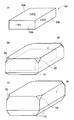
【図1】(a)は、本発明の各実施の形態において使用される、上面が正方形の{100}面で、側面も{100}面である初期の単結晶ダイヤモンド基材を示す斜視図、(b)は、(a)に示した単結晶ダイヤモンド基材に所定の気相成長をさせた場合の成長途中の形状を示す斜視図、(c)は、各側面の下端から成長した傾斜面の上端が、初期の単結晶ダイヤモンド基材の上主表面の高さに到達したときの単結晶ダイヤモンド基材の形状を示す斜視図である。
【図2】(a)は図1(c)に示した単結晶ダイヤモンド基材の下面から傾斜面の上端までを研磨により除去した後の単結晶ダイヤモンド基材の形状を示す斜視図、(b)は(a)に示した単結晶ダイヤモンド基材の上面から、上面四隅の落ち部分が消滅するまで研磨により除去した後の、単結晶ダイヤモンド基材の形状を示す斜視図、(c)は(b)の工程により形成された単結晶ダイヤモンド基材の切出し位置を示す斜視図である。
【図3】(a)は、図1(b)に示した成長途中の単結晶ダイヤモンド基材を、その一つの側面側から見た図、(b)は、図1(b)に示した状態から図1(c)に示した状態に至る成長過程の側面側から見た形状の変化を説明するための模式図である。
【図4】(a)は図1(a)に示した初期の単結晶ダイヤモンド基材の平面図、(b)は図1(b)に示した気相成長途中の単結晶ダイヤモンド基材の平面図、(c)は図2(c)に示した切出し工程前の単結晶ダイヤモンド基材の平面図である。
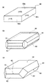
【図5】(a)は、本発明の各実施の形態において使用される、上面が正方形の{100}面で、側面が{110}面である初期の単結晶ダイヤモンド基材を示す斜視図、(b)は、(a)に示した単結晶ダイヤモンド基材に所定の気相成長をさせた場合の成長途中の形状を示す斜視図、(c)は、各側面の上下端から相対向して成長した1対の傾斜面の交線が稜線をなすまでに成長した段階の単結晶ダイヤモンド基材の形状を示す斜視図である。
【図6】(a)は図5(c)に示した単結晶ダイヤモンド基材の上面から、1対の傾斜面の交線がなす稜線を含む平面まで、研磨により除去した後の単結晶ダイヤモンド基材の形状を示す斜視図、(b)は(a)に示した単結晶ダイヤモンド基材の上面を成長開始面として所定の気相成長をさせた後の形状を示す斜視図、(c)は(b)の工程により形成された単結晶ダイヤモンド基材の下面から成長開始面までを研磨により除去の単結晶ダイヤモンド基材の形状を、その後の切出し工程における切出し位置を含めて示す斜視図である。
【図7】(a)は、図5(b)に示した成長途中の単結晶ダイヤモンド基材を、その一つの側面側から見た図、(b)は、図5(b)に示した状態から図5(c)に示した状態に至る成長過程の側面側から見た形状の変化を説明するための模式図である。
【図8】(a)は図5(a)に示した初期の単結晶ダイヤモンド基材の平面図、(b)は図5(b)に示した気相成長途中の単結晶ダイヤモンド基材の平面図、(c)は図6(c)に示した切出し工程前の単結晶ダイヤモンド基材の平面図である。
【図9】基材を切出す段階における基材の側面への単結晶ダイヤモンドの成長厚さの好ましい範囲を説明するための平面図であり、そのうち(a)は、{100}面への〈100〉方向の成長厚さが基材の初期の1辺の長さの約22%に段階で、正方形の切出し線12位置で切断して四角柱状に切出す場合の平面図、(b)は、{100}面への〈100〉方向の成長厚さが、(a)と同様に基材の初期の1辺の長さの約22%に段階で、コーナ部においては切出し線12位置で切断して八角柱状に切出す場合の平面図、(c)は、{100}面への〈100〉方向の気相成長厚さが基材の初期の1辺の長さの約50%になった段階で、正方形の切出し線12位置で切断して四角柱状に切出す場合の平面図である。
【図10】本発明の実施の形態1の実験に使用した、マイクロ波CVD装置の模式図である。
【図11】本発明の実施の形態2の実験に使用した、ダイヤモンド気相合成用の熱フィラメントCVD装置を示す模式図である。
【符号の説明】
1,27 基材ホルダ(基材保持手段)
2,26 単結晶ダイヤモンド基材
3 プラズマ発生領域
4 マイクロ波電源
5 チューナ
6 導波管
7 石英管(反応容器)
8.23 排出口
9,22 導入口
10 プランジャ
11 異常成長領域
21 反応容器
24 交流電源
25 タングステンフィラメント
50,60 初期の単結晶ダイヤモンド基材(素基材)
50a,60a 素基材の主表面
50b,50c,60b,60c 素基材の側面
51,61,62 傾斜面
63 1対の傾斜面の交線がなす稜線
64a 成長開始面[0001]
BACKGROUND OF THE INVENTION
The present invention relates to a method for producing single crystal diamond using a vapor phase synthesis method.To the lawIn particular, a method for producing a relatively large single crystal diamond of about 10 mm × 10 mm or more used for cutting tools, precision tools, semiconductor materials, electronic parts, optical parts, etc.To the lawIt is related.
[0002]
[Prior art]
Since diamond has many excellent properties such as high hardness, high thermal conductivity, and transparency, it is widely used as a material for various tools, optical parts, semiconductors, electronic parts, etc. it is conceivable that.
[0003]
In the past, naturally-occurring diamonds have been used for industrial purposes, but nowadays they are mainly synthesized artificially. Conventionally, polycrystalline diamond has been artificially produced by a gas phase synthesis method such as plasma CVD (Chemical Vapor Deosition) (for example, “Applied Physics, Vol. 55, No. 7, 1986”). , p640 to p653 ”). However, such polycrystalline diamond has a problem that a sufficiently smooth surface cannot be obtained when it is polished because the polycrystalline diamond layer formed on the
[0004]
As a conventional method for producing single crystal diamond using vapor phase synthesis technology, at least one carbon source such as hydrocarbon, carbon oxide, alcohol, acetone, etc. is used as a carbon source, such as hydrogen, oxygen, water, nitrogen, halogen, etc. Using the mixed source gas, the source gas is decomposed and activated using direct current, low frequency alternating current, high frequency, or microwave, and single crystal diamond is gasified on the substrate using low or high temperature plasma. Examples thereof include a plasma vapor deposition method in which phase growth is performed, and a hot filament method in which single crystal diamond is vapor-grown on a substrate using a thermionic emission material such as a tungsten filament heated at high temperature. In addition, when using any of these vapor phase growth methods, depending on the type of substrate used, a method of homoepitaxially growing single crystal diamond on a single crystal diamond substrate, and a non-diamond substrate And a method of heteroepitaxially growing single crystal diamond. Further, in the case of using homoepitaxial growth, mosaic growth using a base material in which a plurality of single crystal diamonds are adjacently joined in the same plane for the purpose of increasing the area of the base material (Japanese Patent Laid-Open No. 3-75298). Gazette, Diamond and Related Material 4 (1995) p1025-1031).
[0005]
[Problems to be solved by the invention]
In conventional homoepitaxial growth, twins and secondary nuclei grow in the middle of growth, resulting in abnormal growth on the sides, and in addition, it does not spread laterally due to polycrystalline diamond growing from the substrate holder. There was a problem. In heteroepitaxial growth, the technology for aligning the top surface has progressed, but the alignment of the in-plane orientation has not been solved so far. Also, in mosaic growth, the joints between single crystal diamond base materials are mismatched and remain as interfaces, and abnormal growth occurs there, so that the single crystal diamond does not become a large area single crystal diamond. There was a problem that the angles had to be perfectly aligned.
[0006]
Conventionally, a material that easily forms a compound by reacting with carbon, such as silicon, silicon carbide, cubic boron nitride, or the like, has been used as a base material holder, so that single crystal diamond grows near the base material. There was the problem of producing polycrystalline diamond that would interfere.
[0007]
In order to eliminate the conventional problems such as these, the present invention is a method for stably producing large-area single crystal diamond by either the plasma CVD method or the hot filament method.The lawThe purpose is to provide.
[0008]
[Means for Solving the Problems]
Solve the above issuesBookThe method for producing a single crystal diamond according to the invention uses a single crystal diamond base material whose main surface and side surfaces are low index surfaces, and is obtained by homoepitaxial vapor growth of the single crystal diamond on the base material. Form single-crystal diamond of areaThe
[0009]
Here, the “low index surface” means {100} {110} {111}, a surface forming an angle within 5 ° with respect to these surfaces, and {311} {331} {511. } {551} {711} planes and all planes forming an angle within 1 ° with respect to these planes.
[0010]
As described above, by using a single crystal diamond substrate whose main surface and side surfaces are low-index surfaces that are stable in terms of energy, single crystal diamond can be stably grown on the substrate surface. As a result, high-quality single crystal diamond having a large area can be formed.
[0012]
In one aspect of the method for producing a single crystal diamond of the present invention,As a single crystal diamond substrate, ThatThe main surface of the surface is a square surface with an inclination with respect to the {100} plane within 5 °, and the four side surfaces have an inclination with respect to the {100} surface within 5 ° or an inclination with respect to the {110} surface within 5 °. Using the face ofThe Further, when the side surface is the {100} plane, <100> plane orientation conditions with a methane concentration of 8% or more and a substrate temperature of 1000 ° C. or less are applied, and when the side surface is the {110} plane, the methane concentration is 3 ± 0.5. % Of methane-hydrogen mixed gas within the range of 100%, and <110> plane orientation conditions maintained within the reaction chamber pressure of 140 ± 5 Torr and the substrate temperature of 1050 ± 10 ° C. are applied..
[0013]
As an index of the vapor growth rate of the single crystal diamond on the side surface of the substrate having such a low index surface, the vapor growth rate V <100> in the <100> direction and the vapor growth rate V <100 in the <111> direction. 111>, that is, a growth rate ratio defined by V <100> / V <111> is used, and the conditions for performing homoepitaxial growth are determined in accordance with the surface orientation of the side surface of the substrate. Specifically, when the side surface of the substrate is a {100} plane, the growth rate ratio is 1.62 or more, particularly preferably 30.5The growth is performed under the above <100> orientation growth conditions. When the side surface is a {110} plane, the growth rate ratio is 0.81 to 0.92, particularly preferably 0.5 × 3.0.5The growth rate ratio is 0.64 or less, particularly preferably 3 when the growth is carried out under the <110> orientation growth conditions and the side faces are {111} faces.-0.5Growth is performed under the following <111> orientation growth conditions. When the side surface is composed of two plane orientations, the growth is performed under conditions matching either plane orientation. As a result, the growth in that direction is the fastest in the extension of the side surface, so that it is difficult to form abnormal growth, and the region including the abnormal growth can be limited.
[0014]
Of the present inventionThe manufacturing method of single crystal diamondHeySimpleAs the crystal diamond base material, the main surface is a square surface having an inclination with respect to the {100} plane within 5 °, and the four side surfaces are those having an inclination with respect to the {100} plane within 5 °, In addition, a vapor growth condition is used in which the vapor growth rate of single crystal diamond with respect to the {111} plane is the fastest.
[0015]
Thus, by using the <111> orientation condition instead of the <110> orientation condition, the thickness of the {110} side surface gradually decreases as the growth proceeds, as in the <110> orientation condition. Therefore, there is an advantage that a single crystal diamond base material having a larger area can be easily formed.
[0016]
The present inventionOne embodimentIn,singleA surface substantially perpendicular to the main surface so that a low-index surface different from the side surface before the vapor phase growth forms a new side surface after vapor-depositing single crystal diamond on the main surface and side surfaces of the crystalline diamond substrate. The single crystal diamond is cut by cutting to remove twin crystals and secondary nuclei that have grown abnormally during homoepitaxial growth.
[0017]
Also,The method for producing single-crystal diamond of the present invention is still another aspect.InsingleA step of cutting out a single crystal diamond having a substantially rectangular parallelepiped shape by cutting a crystal diamond base material having four side surfaces each having an inclination with respect to the {100} plane within 5 ° and cutting the surface substantially perpendicular to the main surface. Before the above, the following steps are further provided. That is, when the upper end of the inclined surface that grows from the lower side of each of the four side surfaces reaches the height of the main surface on the upper side of the single-crystal diamond substrate, or in the previous stage, the lower surface and the inclined surface from the lower surface The method further includes a step of removing, by polishing, a portion between the upper end of the surface and a portion between the upper surface and the lower end of the falling portion of the upper four corners.
[0018]
Thus, when the upper end of the inclined surface that grows from the lower side of each of the four side surfaces reaches the height of the main surface on the upper side of the single crystal diamond base material, or in the previous stage, the removal process by polishing is performed. Even if the inclined surface reaches the upper main surface of the single crystal diamond base material and continues to grow, it is a part that is not necessary in this manufacturing method, and is larger. This is because the result is contrary to the object of the present invention to form the single crystal diamond earlier.
[0019]
However, from the viewpoint of increasing the production efficiency by growing single crystal diamond in the necessary area of the largest area, the inclined surface appearing from the lower side of each of the four side surfaces is the upper side of the single crystal diamond substrate. It is preferable to proceed to the next step at the stage where the surface is reached (the stage where it has grown to the position indicated by the broken line in FIG. 4B).
[0020]
further,The method for producing single-crystal diamond of the present invention is still another aspect.smellSimpleA step of cutting out a single crystal diamond having a substantially rectangular parallelepiped shape by cutting a crystal diamond base material having four side surfaces each having an inclination with respect to the {110} plane within 5 ° and cutting the surface substantially perpendicular to the main surface. Before the above, the following steps are further provided. First, on each of the four side surfaces, a pair of inclined surfaces that are grown vertically opposite to each other and whose inclination with respect to the {111} plane is within 5 °, and a line where the pair of inclined surfaces intersect forms a ridge line When the growth plane parallel to the four side surfaces disappears or at the previous stage, the main surface is grown and removed from the upper plane to the plane including the ridgeline, and {100 } A new growth starting main surface composed of a plane whose inclination with respect to the plane is within 5 ° is formed. Next, single crystal diamond is vapor-phase grown on the main surface of the new growth start.LetThereafter, the area from the lower surface to the new main growth starting surface is removed.
[0021]
As described above, the main surface grows until the line where the pair of inclined surfaces cross each other forms a ridgeline, and the growth surface parallel to the four side surfaces of the single crystal diamond substrate disappears, or at the previous stage. The process of removing the single crystal diamond from the upper surface formed by growing up to the plane including the ridge line, and then cutting out the single crystal diamond, eliminates the growth plane parallel to the four side surfaces of the single crystal diamond substrate. Even if the growth is further continued from the stage of growth (the stage of growth up to the position indicated by the broken line in FIG. 9B), the size of the single crystal diamond surface that can be cut out from the grown single crystal diamond substrate does not increase. This is because the present production method only increases the number of defective polycrystalline diamond portions, which is contrary to the object of the present invention for forming a larger single crystal diamond earlier. However, from the viewpoint of increasing the manufacturing efficiency by maximizing the area of the single crystal diamond that can be cut out, the process proceeds to the next step when each of the four side surfaces has just disappeared due to the growth of the pair of inclined surfaces. It is preferable to do so.
[0022]
Also,The method for producing single-crystal diamond of the present invention is still another aspect.In, mainThe above-mentioned process of cutting a single crystal diamond having a substantially rectangular parallelepiped shape by cutting a surface substantially perpendicular to the surface, {When a surface with an inclination with respect to the 100} plane is within 5 ° constitutes the side surface before cutting, the surface with an inclination with respect to the {110} plane within 5 ° is cut out to form a new side surface, and the {110} surface In the case where a surface having an inclination with respect to 5 ° or less constitutes a side surface before cutting, a step of cutting so that a surface having an inclination with respect to the {100} surface within 5 ° becomes a new side surface is included.
[0023]
Also, the method for producing single crystal diamond of the present inventionPreferred embodiment ofIn, CutCutting the single crystal diamond whose side surface before cutting is a surface with an inclination with respect to the {100} plane within 5 ° so that the surface with an inclination with respect to the {110} surface within 5 ° constitutes a new side surface; Cut the single crystal diamond whose side face before cutting is a plane whose inclination with respect to the {110} face is within 5 °, so that the new side face forms a new side face with the inclination within 5 ° relative to the {100} face. A large-area single crystal diamond is formed by alternately repeating the step of taking out.
[0027]
DETAILED DESCRIPTION OF THE INVENTION
Embodiments of the present invention will be described below with reference to the drawings.
[0028]
(Embodiment 1)
FIG. 10 is a schematic diagram showing a microwave CVD apparatus for diamond vapor phase synthesis used in the experiment according to
[0029]
As shown in FIGS. 1 (a) and 4 (a), the
[0030]
Thereafter, as shown in FIG. 1C, the {100} side surface is grown without abnormal growth, and the upper end of the
[0031]
Next, the growth condition is a growth rate ratio of 0.5 × 30.5<110> Preferential orientation growth conditions, specifically, a methane-hydrogen mixed gas with a methane concentration of 3 ± 0.5% was used, and the pressure in the reaction vessel was maintained at 140 ± 5 Torr and the substrate temperature was 1050 ± 10 ° C. When grown under the conditions, it grew as shown in FIGS. 5 (b) and 7 (a). From the upper and lower ends of the four side surfaces of the
[0032]
Then, in order to cause a surface without abnormal growth to appear as a surface, as shown in FIG. 5 (c), it has grown until the intersecting line of the upper and lower
[0033]
In the present embodiment, in the homoepitaxial growth process using the single crystal substrate having the {110} side surface shown in FIG. 5A as the base material, the <110> preferred orientation growth conditions were used. For the following reasons, the object of the present invention can also be achieved by using <111> preferred orientation growth conditions in which the growth rate in the <111> direction is the fastest instead of <110> preferred orientation growth conditions.
[0034]
It is generally known that an isolated particle of diamond formed by homoepitaxial growth from a point is usually composed of two types of planes, a {100} plane and a {111} plane. This is because growth in the <100> direction on the {100} plane and growth in the <111> direction on the {111} plane mainly occur, and growth on the other planes is relatively difficult. Therefore, the growth rate ratio as an index for specifying each orientation growth condition is defined as the ratio between the vapor growth rate V <100> in the <100> direction and the vapor growth rate V <111> in the <111> direction. As can be seen, it is known that the growth rate to other low index planes is determined by the magnitude relationship between the growth rates in the <110> direction and the <111> direction.
[0035]
As described above, when the <110> preferred orientation growth condition is applied to the substrate shown in FIG. 5A, the growth rate ratio is 0.5 × 3.0.5Thus, since the vapor growth rate in the <111> direction is faster than the vapor growth rate in the <100> direction, the influence of the vapor growth in the <111> direction is large. Therefore, the shape after the vapor phase growth is as shown in FIG. 7A, and as the growth proceeds, the thickness of the {110} plane is gradually reduced as shown in FIG. The thickness of the region where no abnormal growth occurs is also reduced. However, if the <111> preferred orientation growth condition is applied to the substrate shown in FIG. 5A instead of the <110> preferred orientation growth condition, the thickness of the region where no abnormal growth occurs is reduced. It is possible to grow without. That is, when homoepitaxial growth is performed on a base material having a {100} plane and a {110} plane on the main surface, the growth rate on the side is the fastest. The object of the present invention can also be achieved by applying growth conditions.
[0036]
Next, a method for obtaining single crystal diamond having the largest area in the cutting process using the YAG laser in this embodiment will be described. In the cutting process using a YAG laser at the position of the cutting
[0037]
A preferable range of the growth thickness of the single crystal diamond on the side surface of the substrate in the step of cutting the substrate is described as follows with reference to FIG. First, when the growth thickness in the <100> direction on the {100} plane is about 22% of the initial length of one side of the substrate, the positions of the cut lines 12 forming each square piece, that is, the four corners are { Consider a case of cutting into a quadrangular prism shape with the abnormally grown
[0038]
However, even when the growth thickness in the <100> direction on the {100} plane does not exceed about 22% of the initial length of one side of the substrate, as shown in FIG. The corner portion is cut at the position of the cutting
[0039]
Further, when the growth thickness in the <100> direction on the {100} plane is about 50% of the initial length of one side of the substrate, the positions of the square cut lines 12, that is, the four corners are the {110} planes. When cutting and cutting into a quadrangular prism shape with the abnormally grown
[0040]
(Embodiment 2)
Next, a second embodiment of the present invention in which a diamond single crystal is vapor-phase synthesized by applying a hot filament method will be described.
[0041]
FIG. 11 is a schematic diagram showing a hot filament CVD apparatus for diamond vapor phase synthesis used in the experiment. In the hot filament CVD apparatus shown in FIG. 1, a
[0042]
As in the first embodiment, as the single crystal diamond base material 26, the
[0043]
Thereafter, as shown in FIG. 1C, the {100} side surface is grown without abnormal growth, and the upper end of the
[0044]
Next, the growth condition is a growth rate ratio of 0.5 × 30.5<110> Preferentially oriented growth conditions, specifically, using a methane-hydrogen mixed gas having a methane concentration of 1.2%, and growing under the conditions of maintaining the pressure in the reaction vessel at 100 Torr and the substrate temperature of 850 ° C. As shown in FIG. 5B and FIG. From the upper and lower ends of the four side surfaces of the
[0045]
Then, in order to cause a surface without abnormal growth to appear as a surface, as shown in FIG. 5 (c), it has grown until the intersecting line of the upper and lower
[0046]
Also in the case of the present embodiment, as in the case of the first embodiment, when homoepitaxial growth is performed on a base material whose main surface is {100} plane and side surface is {110} plane, growth on the side surface is performed. It goes without saying that the object of the present invention can also be achieved by applying <111> orientation growth conditions different from the <110> orientation growth conditions at which the speed is highest.
[0047]
In each of the above embodiments, the main surface and each side surface of the base material, the surface grown by vapor phase growth, and the surface orientation of the cut surface in the cutting step are {100} plane, {110} plane, Although described with respect to {111} planes, etc., it is not always necessary to coincide with such plane orientations, and the plane orientations of these planes are within the range included in the definition of the low index plane described above. If it is a plane orientation, the object of the present invention can be achieved.
[0048]
In addition, it should be considered that the embodiment disclosed this time is illustrative in all points and not restrictive. The scope of the present invention is shown not by the above description but by the appended claims, and is intended to include all modifications within the meaning and scope equivalent to the claims.
[0049]
【The invention's effect】
As described above, according to the present invention, the base material is epitaxially grown and grown while cutting out only a region having no abnormal growth such as twins and secondary nuclei. By suppressing precipitation, it is possible to eliminate the secondary diamond that grows from the substrate holder into the laterally grown diamond, making it possible to produce large-area single crystal diamonds. Become. This opens up the possibility of developing new products such as large-diameter single-crystal diamond windows and single-crystal diamond wafers that were previously impossible.
[Brief description of the drawings]
FIG. 1 (a) is a perspective view showing an initial single crystal diamond substrate used in each embodiment of the present invention, whose upper surface is a square {100} face and whose side face is also a {100} face. (B) is a perspective view showing a shape during growth when the single crystal diamond base material shown in (a) is subjected to predetermined vapor phase growth, and (c) is an inclination grown from the lower end of each side surface. It is a perspective view which shows the shape of a single crystal diamond base material when the upper end of a surface reaches the height of the upper main surface of an initial single crystal diamond base material.
2A is a perspective view showing the shape of a single crystal diamond substrate after polishing from the lower surface of the single crystal diamond substrate shown in FIG. 1C to the upper end of the inclined surface by polishing; FIG. ) Is a perspective view showing the shape of the single crystal diamond substrate after removal by polishing from the upper surface of the single crystal diamond substrate shown in FIG. It is a perspective view which shows the cutting-out position of the single crystal diamond base material formed by the process of b).
3A is a view of the single crystal diamond substrate in the middle of growth shown in FIG. 1B as seen from one side surface thereof, and FIG. 3B is a view shown in FIG. 1B. It is a schematic diagram for demonstrating the change of the shape seen from the side surface of the growth process from a state to the state shown in FIG.1 (c).
4A is a plan view of the initial single crystal diamond base material shown in FIG. 1A, and FIG. 4B is a plan view of the single crystal diamond base material during vapor phase growth shown in FIG. 1B. FIG. 2C is a plan view of the single crystal diamond base material before the cutting step shown in FIG.
FIG. 5 (a) is a perspective view showing an initial single crystal diamond base material having a {100} plane having a square top surface and a {110} plane having a square top surface used in each embodiment of the present invention. (B) is a perspective view which shows the shape in the middle of the growth at the time of making predetermined vapor phase growth to the single-crystal diamond base material shown to (a), (c) is opposite from each side from the upper and lower ends It is a perspective view which shows the shape of the single crystal diamond base material of the stage grown until the intersection line of a pair of inclined surface which grew up makes a ridgeline.
6A is a view of single crystal diamond after removing from the top surface of the single crystal diamond base material shown in FIG. 5C to a plane including a ridge line formed by the intersection of a pair of inclined surfaces by polishing. FIG. The perspective view which shows the shape of a base material, (b) is a perspective view which shows the shape after carrying out predetermined vapor phase growth by making the upper surface of the single crystal diamond base material shown to (a) into a growth start surface, (c) FIG. 3B is a perspective view showing the shape of the single crystal diamond base material from which the bottom surface of the single crystal diamond base material formed by the step (b) to the growth start surface is removed by polishing, including the cutting position in the subsequent cutting step. is there.
7A is a view of the single crystal diamond substrate in the middle of growth shown in FIG. 5B as viewed from one side surface thereof, and FIG. 7B is a view shown in FIG. 5B. It is a schematic diagram for demonstrating the change of the shape seen from the side surface of the growth process from a state to the state shown in FIG.5 (c).
8A is a plan view of the initial single crystal diamond base material shown in FIG. 5A, and FIG. 8B is a plan view of the single crystal diamond base material during vapor phase growth shown in FIG. 5B. FIG. 6C is a plan view of the single crystal diamond base material before the cutting step shown in FIG.
FIG. 9 is a plan view for explaining a preferred range of the growth thickness of single-crystal diamond on the side surface of the base material at the stage of cutting out the base material, in which (a) shows the <100} plane < FIG. 10B is a plan view in the case where the growth thickness in the 100> direction is about 22% of the initial length of one side of the base material and is cut at a
FIG. 10 is a schematic diagram of a microwave CVD apparatus used in the experiment of
FIG. 11 is a schematic diagram showing a hot filament CVD apparatus for diamond vapor phase synthesis used in the experiment of
[Explanation of symbols]
1,27 Base material holder (base material holding means)
2,26 Single crystal diamond base material
3 Plasma generation region
4 Microwave power supply
5 Tuner
6 Waveguide
7 Quartz tube (reaction vessel)
8.23 outlet
9,22 Introduction port
10 Plunger
11 Abnormal growth area
21 reaction vessel
24 AC power supply
25 Tungsten filament
50,60 Early single crystal diamond base material (base material)
50a, 60a Main surface of base material
50b, 50c, 60b, 60c Side surface of base material
51, 61, 62 Inclined surface
63 Ridge line formed by the intersection of a pair of inclined surfaces
64a Growth start surface
Claims (7)
前記単結晶ダイヤモンド基材として、その主表面が{100}面に対する傾きが5°以内の正方形の面からなり、4つの側面が{100}面に対する傾きが5°以内の面または{110}面に対する傾きが5°以内の面からなるものを用い、側面が{100}面のときはメタン濃度8%以上、基板温度1000℃以下の〈100〉面配向条件を適用し、側面が{110}面のときは、メタン濃度3±0.5%の範囲内のメタン−水素系混合ガスを用い、反応容器内圧力140±5Torr、基材温度1050±10℃の範囲内に維持した〈110〉面配向条件を適用する、単結晶ダイヤモンドの製造方法。 A method for producing a single crystal diamond by synthesizing single crystal diamond from a gas phase on a single crystal diamond base material, wherein the single crystal diamond base material has a main surface and side surfaces made of low index surfaces,
As the single crystal diamond base material, the main surface is a square surface whose inclination with respect to the {100} plane is 5 ° or less, and the four side surfaces are surfaces whose inclination with respect to the {100} plane is within 5 ° or {110} planes When the side surface is a {100} plane, a <100> plane orientation condition with a methane concentration of 8% or more and a substrate temperature of 1000 ° C. or less is applied, and the side surface is {110} In the case of the surface , a methane-hydrogen mixed gas having a methane concentration in the range of 3 ± 0.5% was used, and the pressure in the reaction vessel was maintained in the range of 140 ± 5 Torr and the substrate temperature in the range of 1050 ± 10 ° C. <110> A method for producing single-crystal diamond, wherein plane orientation conditions are applied.
前記単結晶ダイヤモンド基材として、その主表面が{100}面に対する傾きが5°以内の正方形の面からなり、4つの側面が、{110}面に対する傾きが5°以内の面からなるものを用い、かつ、{111}面方位に対する単結晶ダイヤモンドの気相成長速度が〈100〉方向への成長速度と比べて30.5 倍以上の速さである、メタン濃度1.5%以下、基板温度1100℃以上の〈111〉配向条件を使用する、単結晶ダイヤモンドの製造方法。 A method for producing a single crystal diamond by synthesizing single crystal diamond from a gas phase on a single crystal diamond base material, wherein the single crystal diamond base material has a main surface and side surfaces made of low index surfaces,
As the single crystal diamond base material, the main surface is a square surface with an inclination with respect to the {100} plane within 5 °, and the four side surfaces are surfaces with an inclination with respect to the {110} plane within 5 °. Used, and the vapor growth rate of the single crystal diamond with respect to the {111} plane orientation is 30.5 times faster than the growth rate in the <100> direction, the methane concentration is 1.5% or less, the substrate temperature A method for producing single crystal diamond using <111> orientation conditions of 1100 ° C. or higher.
前記単結晶ダイヤモンド基材の前記主表面および前記側面に単結晶ダイヤモンドを気相成長させた後に、気相成長前の側面と異なる低指数面が新たな側面を構成するように、少なくとも前記主表面に略垂直な面で切断する工程を含むことによって単結晶ダイヤモンドを切出し、
前記単結晶ダイヤモンド基材として、{100}面に対する傾きが5°以内の面からなる4つの側面からなるものを用い、前記主表面に略垂直な面で切断して略直方体形状の単結晶ダイヤモンドを切出す工程の前に、前記4つの側面の各々の下側から成長する傾斜面の上端が前記単結晶ダイヤモンド基材の上側の主表面の高さに到達したとき、またはその前の段階で、下面と、下面からの傾斜面の上端との間の部分、および、上面と、上面四隅の落ち部分の下端との間の部分を、研磨により除去する工程をさらに備えた、単結晶ダイヤモンドの製造方法。 A method for producing a single crystal diamond by synthesizing single crystal diamond from a gas phase on a single crystal diamond base material, wherein the single crystal diamond base material has a main surface and side surfaces made of low index surfaces,
After vapor-depositing single crystal diamond on the main surface and the side surface of the single crystal diamond base material, at least the main surface so that a low index surface different from the side surface before the vapor phase growth forms a new side surface A single crystal diamond is cut out by including a step of cutting at a plane substantially perpendicular to
As the single-crystal diamond base material, a single-crystal diamond having a substantially rectangular parallelepiped shape cut by a plane substantially perpendicular to the main surface is used which has four side faces each having an inclination with respect to the {100} plane within 5 °. Before the step of cutting out, when the upper end of the inclined surface that grows from the lower side of each of the four side surfaces reaches the height of the upper main surface of the single crystal diamond substrate, or in the previous stage , portions between the lower surface, the upper end of the inclined surface from the lower surface, and upper and, a portion between the lower end of the falling portion of the top surface corner, further comprising the step of removing by polishing the single crystal diamond Production method.
前記単結晶ダイヤモンド基材の前記主表面および前記側面に単結晶ダイヤモンドを気相成長させた後に、気相成長前の側面と異なる低指数面が新たな側面を構成するように、少なくとも前記主表面に略垂直な面で切断する工程を含むことによって単結晶ダイヤモンドを切出し、
前記単結晶ダイヤモンド基材として、{110}面に対する傾きが5°以内の面からなる4つの側面からなるものを用い、前記主表面に略垂直な面で切断して略直方体形状の単結晶ダイヤモンドを切り出す工程の前に、前記4つの側面の各々に、上下に対向して成長する、{111}面に対する傾きが5°以内の1対の傾斜面が、該1対の傾斜面同士が交わる線が稜線をなすまで成長して、前記4つの側面に平行な成長面が消失するとき、またはその前の段階で、前記主表面が成長して形成された上側の面から、前記稜線を含む平面まで除去して、{100}面に対する傾きが5°以内の面からなる新たな成長開始主表面を形成する工程と、前記新たな成長開始主表面上に、単結晶ダイヤモンドを気相成長させる工程と、下面から前記新たな成長開始主表面までを除去する工程とをさらに備えた、単結晶ダイヤモンドの製造方法。 A method for producing a single crystal diamond by synthesizing single crystal diamond from a gas phase on a single crystal diamond base material, wherein the single crystal diamond base material has a main surface and side surfaces made of low index surfaces,
After vapor-depositing single crystal diamond on the main surface and the side surface of the single crystal diamond base material, at least the main surface so that a low index surface different from the side surface before the vapor phase growth forms a new side surface A single crystal diamond is cut out by including a step of cutting at a plane substantially perpendicular to
As the single-crystal diamond base material, a single-crystal diamond having a substantially rectangular parallelepiped shape cut by a plane substantially perpendicular to the main surface is used which has four side faces each having an inclination with respect to the {110} plane within 5 °. Before the step of cutting out, a pair of inclined surfaces, which grow up opposite to each other on each of the four side surfaces and have an inclination with respect to the {111} plane within 5 °, intersect the pair of inclined surfaces. When the line grows to form a ridgeline and the growth plane parallel to the four side surfaces disappears or in the previous stage, the main surface includes the ridgeline from the upper surface formed by growth. Removing a flat surface and forming a new growth starting main surface having a surface whose inclination with respect to the {100} plane is within 5 °; and vapor-depositing single crystal diamond on the new growth starting main surface Process and the new process from the bottom. Starting main to the surface, further comprising a step of removing, the method for producing a single crystal diamond.
前記単結晶ダイヤモンド基材の前記主表面および前記側面に単結晶ダイヤモンドを気相成長させた後に、気相成長前の側面と異なる低指数面が新たな側面を構成するように、少なくとも前記主表面に略垂直な面で切断する工程を含むことによって単結晶ダイヤモンドを切出し、
前記主表面に略垂直な面で切断して略直方体形状の単結晶ダイヤモンドを切出す前記工程が、{100}面に対する傾きが5°以内の面が切断前の側面を構成する場合には、{110}面に対する傾きが5°以内の面が新たな側面を構成するように切出し、{110}面に対する傾きが5°以内の面が切断前の側面を構成する場合には、{100}面に対する傾きが5°以内の面が新たな側面になるように切出す工程を含む、単結晶ダイヤモンドの製造方法。 A method for producing a single crystal diamond by synthesizing single crystal diamond from a gas phase on a single crystal diamond base material, wherein the single crystal diamond base material has a main surface and side surfaces made of low index surfaces,
After vapor-depositing single crystal diamond on the main surface and the side surface of the single crystal diamond base material, at least the main surface so that a low index surface different from the side surface before the vapor phase growth forms a new side surface A single crystal diamond is cut out by including a step of cutting at a plane substantially perpendicular to
When the step of cutting single-crystal diamond having a substantially rectangular parallelepiped shape by cutting along a plane substantially perpendicular to the main surface is a side whose inclination with respect to the {100} plane is within 5 ° constitutes the side surface before cutting, When a surface having an inclination with respect to the {110} plane is within 5 ° forms a new side surface, and a surface with an inclination with respect to the {110} surface within 5 ° forms a side surface before cutting, {100} A method for producing single crystal diamond, comprising a step of cutting so that a surface having an inclination with respect to a surface of 5 ° or less becomes a new side surface.
Priority Applications (4)
| Application Number | Priority Date | Filing Date | Title |
|---|---|---|---|
| JP04332598A JP4032482B2 (en) | 1997-04-18 | 1998-02-25 | Method for producing single crystal diamond |
| US09/060,555 US6096129A (en) | 1997-04-18 | 1998-04-15 | Method of and apparatus for producing single-crystalline diamond of large size |
| EP98302982A EP0879904B1 (en) | 1997-04-18 | 1998-04-17 | Method and apparatus for producing single-crystalline diamond |
| DE69802037T DE69802037T2 (en) | 1997-04-18 | 1998-04-17 | Method and device for producing single-crystal diamond |
Applications Claiming Priority (3)
| Application Number | Priority Date | Filing Date | Title |
|---|---|---|---|
| JP10161397 | 1997-04-18 | ||
| JP9-101613 | 1997-04-18 | ||
| JP04332598A JP4032482B2 (en) | 1997-04-18 | 1998-02-25 | Method for producing single crystal diamond |
Publications (2)
| Publication Number | Publication Date |
|---|---|
| JPH111392A JPH111392A (en) | 1999-01-06 |
| JP4032482B2 true JP4032482B2 (en) | 2008-01-16 |
Family
ID=26383082
Family Applications (1)
| Application Number | Title | Priority Date | Filing Date |
|---|---|---|---|
| JP04332598A Expired - Lifetime JP4032482B2 (en) | 1997-04-18 | 1998-02-25 | Method for producing single crystal diamond |
Country Status (4)
| Country | Link |
|---|---|
| US (1) | US6096129A (en) |
| EP (1) | EP0879904B1 (en) |
| JP (1) | JP4032482B2 (en) |
| DE (1) | DE69802037T2 (en) |
Families Citing this family (41)
| Publication number | Priority date | Publication date | Assignee | Title |
|---|---|---|---|---|
| US8591856B2 (en) | 1998-05-15 | 2013-11-26 | SCIO Diamond Technology Corporation | Single crystal diamond electrochemical electrode |
| US6858080B2 (en) | 1998-05-15 | 2005-02-22 | Apollo Diamond, Inc. | Tunable CVD diamond structures |
| US6582513B1 (en) | 1998-05-15 | 2003-06-24 | Apollo Diamond, Inc. | System and method for producing synthetic diamond |
| CA2412855C (en) * | 2000-06-15 | 2009-10-20 | Element Six (Pty) Ltd. | Thick single crystal diamond layer method for making it and gemstones produced from the layer |
| CN1243855C (en) | 2000-06-15 | 2006-03-01 | 六号元素(控股)公司 | Single crystal diamond prepared by CVD |
| JP2004538230A (en) * | 2001-08-08 | 2004-12-24 | アポロ ダイアモンド,インコーポレイティド | System and method for producing synthetic diamond |
| GB0130004D0 (en) | 2001-12-14 | 2002-02-06 | Diamanx Products Ltd | Coloured diamond |
| GB0130005D0 (en) * | 2001-12-14 | 2002-02-06 | Diamanx Products Ltd | Boron doped diamond |
| US7060130B2 (en) * | 2002-08-27 | 2006-06-13 | Board Of Trustees Of Michigan State University | Heteroepitaxial diamond and diamond nuclei precursors |
| AU2003259418A1 (en) * | 2002-09-06 | 2004-03-29 | Element Six Limited | Coloured diamond |
| GB0221949D0 (en) * | 2002-09-20 | 2002-10-30 | Diamanx Products Ltd | Single crystal diamond |
| GB0227261D0 (en) | 2002-11-21 | 2002-12-31 | Element Six Ltd | Optical quality diamond material |
| GB0303860D0 (en) | 2003-02-19 | 2003-03-26 | Element Six Ltd | CVD diamond in wear applications |
| DE602004016394D1 (en) | 2003-12-12 | 2008-10-16 | Element Six Ltd | METHOD OF INSERTING A MARKER IN A CVD DIAMOND |
| WO2005061400A1 (en) | 2003-12-12 | 2005-07-07 | Element Six Limited | Method of incorporating a mark in cvd diamond |
| JP5163920B2 (en) * | 2005-03-28 | 2013-03-13 | 住友電気工業株式会社 | Diamond single crystal substrate manufacturing method and diamond single crystal substrate |
| JP5002982B2 (en) * | 2005-04-15 | 2012-08-15 | 住友電気工業株式会社 | Method for producing single crystal diamond |
| JP5594613B2 (en) * | 2005-04-15 | 2014-09-24 | 住友電気工業株式会社 | Single crystal diamond and method for producing the same |
| JP4613314B2 (en) * | 2005-05-26 | 2011-01-19 | 独立行政法人産業技術総合研究所 | Single crystal manufacturing method |
| CA2607202C (en) | 2005-06-22 | 2014-06-03 | Element Six Limited | High colour diamond layer |
| US7399358B2 (en) * | 2005-09-05 | 2008-07-15 | Rajneesh Bhandari | Synthesis of large homoepitaxial monocrystalline diamond |
| JP4873368B2 (en) * | 2007-01-24 | 2012-02-08 | 住友電気工業株式会社 | Diamond substrate |
| GB0704516D0 (en) | 2007-03-08 | 2007-04-18 | Element Six Ltd | Diamond |
| US8342164B2 (en) * | 2008-05-09 | 2013-01-01 | SCIO Diamond Technology Corporation | Gemstone production from CVD diamond plate |
| GB0813490D0 (en) | 2008-07-23 | 2008-08-27 | Element Six Ltd | Solid state material |
| GB0813491D0 (en) | 2008-07-23 | 2008-08-27 | Element Six Ltd | Diamond Material |
| GB0900771D0 (en) | 2009-01-16 | 2009-03-04 | Element Six Ltd | Diamond |
| GB2476306B (en) * | 2009-12-21 | 2012-07-11 | Element Six Ltd | Single crystal diamond material |
| US9157170B2 (en) | 2009-12-21 | 2015-10-13 | Element Six Technologies Limited | Single crystal diamond material |
| US9017633B2 (en) * | 2010-01-18 | 2015-04-28 | Element Six Technologies Limited | CVD single crystal diamond material |
| GB201000768D0 (en) | 2010-01-18 | 2010-03-03 | Element Six Ltd | CVD single crystal diamond material |
| JP5831796B2 (en) * | 2011-09-06 | 2015-12-09 | 住友電気工業株式会社 | Diamond composite, single crystal diamond separated therefrom, and method for producing diamond composite |
| WO2014028831A1 (en) * | 2012-08-17 | 2014-02-20 | Gtat Corporation | System and method of growing silicon ingots from seeds in a crucible and manufacture of seeds used therein |
| EP3054036B1 (en) | 2013-09-30 | 2021-03-03 | Adamant Namiki Precision Jewel Co., Ltd. | Diamond substrate manufacturing method |
| CN108908762A (en) * | 2018-06-15 | 2018-11-30 | 西安碳星半导体科技有限公司 | CVD growth Gem Grade thickness single-crystal diamond cutting method |
| CN110789011A (en) * | 2019-11-07 | 2020-02-14 | 北京昌日新能源科技有限公司 | Novel photovoltaic right-angle monocrystalline silicon piece and manufacturing method thereof |
| CN111690981B (en) * | 2020-07-23 | 2021-08-03 | 太原理工大学 | Method for enlarging size and number of single crystal diamond seed crystals |
| CN111850682B (en) * | 2020-07-23 | 2021-09-07 | 太原理工大学 | Method for simultaneously enlarging size and number of single crystal diamond seed crystals |
| US11878354B2 (en) * | 2020-12-24 | 2024-01-23 | Sumitomo Electric Hardmetal Corp. | Method of manufacturing diamond tool intermediate and method of making determination for single-crystal diamond |
| GB2609023A (en) * | 2021-07-18 | 2023-01-25 | Lusix Ltd | Growing of diamonds |
| CN114232091B (en) * | 2021-12-27 | 2024-05-10 | 苏州贝莱克金刚石科技有限公司 | Large-size single crystal diamond and preparation method thereof |
Family Cites Families (5)
| Publication number | Priority date | Publication date | Assignee | Title |
|---|---|---|---|---|
| JPH01103993A (en) * | 1987-10-16 | 1989-04-21 | Sumitomo Electric Ind Ltd | Method for growing diamond single crystal |
| JPH01103994A (en) * | 1987-10-16 | 1989-04-21 | Sumitomo Electric Ind Ltd | Method for growing diamond single crystal |
| US5127983A (en) * | 1989-05-22 | 1992-07-07 | Sumitomo Electric Industries, Ltd. | Method of producing single crystal of high-pressure phase material |
| US5474021A (en) * | 1992-09-24 | 1995-12-12 | Sumitomo Electric Industries, Ltd. | Epitaxial growth of diamond from vapor phase |
| WO1994016125A1 (en) * | 1993-01-14 | 1994-07-21 | Sumitomo Electric Industries, Ltd. | Process for vapor-phase diamond synthesis |
-
1998
- 1998-02-25 JP JP04332598A patent/JP4032482B2/en not_active Expired - Lifetime
- 1998-04-15 US US09/060,555 patent/US6096129A/en not_active Expired - Lifetime
- 1998-04-17 EP EP98302982A patent/EP0879904B1/en not_active Expired - Lifetime
- 1998-04-17 DE DE69802037T patent/DE69802037T2/en not_active Expired - Lifetime
Also Published As
| Publication number | Publication date |
|---|---|
| US6096129A (en) | 2000-08-01 |
| EP0879904A1 (en) | 1998-11-25 |
| JPH111392A (en) | 1999-01-06 |
| EP0879904B1 (en) | 2001-10-17 |
| DE69802037T2 (en) | 2002-03-14 |
| DE69802037D1 (en) | 2001-11-22 |
Similar Documents
| Publication | Publication Date | Title |
|---|---|---|
| JP4032482B2 (en) | Method for producing single crystal diamond | |
| JP4613314B2 (en) | Single crystal manufacturing method | |
| JP5601634B2 (en) | Method for producing large area CVD diamond single crystal and large area CVD diamond single crystal obtained thereby | |
| JPH0375298A (en) | Production of single crystal of high-pressure phase substance | |
| JPH06247793A (en) | Single crystalline diamond and its production | |
| US10822718B2 (en) | Method for producing aluminum nitride single crystal substrate | |
| JPH06263595A (en) | Diamond-coated material and its production | |
| JP2017214284A (en) | Diamond substrate and method for manufacturing the same | |
| JP5003442B2 (en) | Method for producing diamond single crystal substrate | |
| JPH06107494A (en) | Vapor growth method for diamond | |
| JPH0748198A (en) | Method for synthesizing diamond | |
| US20220127751A1 (en) | Large area single crystal diamond | |
| JP3728464B2 (en) | Method for manufacturing substrate for vapor phase synthesis of single crystal diamond film | |
| Zhu et al. | Evolution of growth characteristics around the junction in the mosaic diamond | |
| US20230392283A1 (en) | Method of Growing Single Crystal Diamond Assisted by Polycrystalline Diamond Growth | |
| Findeling-Dufour et al. | Study for fabricating large area diamond single-crystal layers | |
| JPH0687691A (en) | Production of diamond and diamond single crystal substrate used in the same | |
| JP7487702B2 (en) | Method for manufacturing single crystal diamond substrate | |
| CN117779205B (en) | Method for improving quality of diamond spliced part | |
| JPH06227895A (en) | Synthesis of diamond | |
| TW202428952A (en) | Method for producing a monocrystalline diamond plate, monocrystalline diamond plate and large-size monocrystalline diamond wafer | |
| JPH06172089A (en) | Synthesis of diamond | |
| JP2001335934A (en) | Method for reducing slip in thin film on cubic silicon carbide single crystal | |
| JP3852783B1 (en) | Crystal epitaxial substrate | |
| CN117448950A (en) | Method for reducing mutual interference of diamond crystal growth based on edge laser etching treatment |
Legal Events
| Date | Code | Title | Description |
|---|---|---|---|
| A521 | Request for written amendment filed |
Free format text: JAPANESE INTERMEDIATE CODE: A523 Effective date: 20050113 |
|
| A621 | Written request for application examination |
Free format text: JAPANESE INTERMEDIATE CODE: A621 Effective date: 20050113 |
|
| A977 | Report on retrieval |
Free format text: JAPANESE INTERMEDIATE CODE: A971007 Effective date: 20070711 |
|
| A131 | Notification of reasons for refusal |
Free format text: JAPANESE INTERMEDIATE CODE: A131 Effective date: 20070717 |
|
| A521 | Request for written amendment filed |
Free format text: JAPANESE INTERMEDIATE CODE: A523 Effective date: 20070830 |
|
| TRDD | Decision of grant or rejection written | ||
| A01 | Written decision to grant a patent or to grant a registration (utility model) |
Free format text: JAPANESE INTERMEDIATE CODE: A01 Effective date: 20071002 |
|
| A61 | First payment of annual fees (during grant procedure) |
Free format text: JAPANESE INTERMEDIATE CODE: A61 Effective date: 20071015 |
|
| FPAY | Renewal fee payment (event date is renewal date of database) |
Free format text: PAYMENT UNTIL: 20101102 Year of fee payment: 3 |
|
| R150 | Certificate of patent or registration of utility model |
Free format text: JAPANESE INTERMEDIATE CODE: R150 |
|
| FPAY | Renewal fee payment (event date is renewal date of database) |
Free format text: PAYMENT UNTIL: 20111102 Year of fee payment: 4 |
|
| FPAY | Renewal fee payment (event date is renewal date of database) |
Free format text: PAYMENT UNTIL: 20111102 Year of fee payment: 4 |
|
| FPAY | Renewal fee payment (event date is renewal date of database) |
Free format text: PAYMENT UNTIL: 20121102 Year of fee payment: 5 |
|
| FPAY | Renewal fee payment (event date is renewal date of database) |
Free format text: PAYMENT UNTIL: 20121102 Year of fee payment: 5 |
|
| FPAY | Renewal fee payment (event date is renewal date of database) |
Free format text: PAYMENT UNTIL: 20131102 Year of fee payment: 6 |
|
| R250 | Receipt of annual fees |
Free format text: JAPANESE INTERMEDIATE CODE: R250 |
|
| R250 | Receipt of annual fees |
Free format text: JAPANESE INTERMEDIATE CODE: R250 |
|
| R250 | Receipt of annual fees |
Free format text: JAPANESE INTERMEDIATE CODE: R250 |
|
| R250 | Receipt of annual fees |
Free format text: JAPANESE INTERMEDIATE CODE: R250 |
|
| EXPY | Cancellation because of completion of term |