JP4458906B2 - Semiconductor device - Google Patents
Semiconductor device Download PDFInfo
- Publication number
- JP4458906B2 JP4458906B2 JP2004111380A JP2004111380A JP4458906B2 JP 4458906 B2 JP4458906 B2 JP 4458906B2 JP 2004111380 A JP2004111380 A JP 2004111380A JP 2004111380 A JP2004111380 A JP 2004111380A JP 4458906 B2 JP4458906 B2 JP 4458906B2
- Authority
- JP
- Japan
- Prior art keywords
- semiconductor
- heat
- semiconductor device
- insulating film
- interlayer insulating
- Prior art date
- Legal status (The legal status is an assumption and is not a legal conclusion. Google has not performed a legal analysis and makes no representation as to the accuracy of the status listed.)
- Expired - Fee Related
Links
Images


Classifications
-
- H—ELECTRICITY
- H01—ELECTRIC ELEMENTS
- H01L—SEMICONDUCTOR DEVICES NOT COVERED BY CLASS H10
- H01L2924/00—Indexing scheme for arrangements or methods for connecting or disconnecting semiconductor or solid-state bodies as covered by H01L24/00
- H01L2924/0001—Technical content checked by a classifier
- H01L2924/0002—Not covered by any one of groups H01L24/00, H01L24/00 and H01L2224/00
Description
この発明は、一般的には、半導体装置に関し、より特定的には、半導体素子から発生した熱を冷却または放熱する構造を備えた半導体装置に関する。 The present invention generally relates to semiconductor devices, and more particularly to a semiconductor device having a structure for cooling or radiating heat generated from a semiconductor element.
従来、ヒートスプレッダと呼ばれる熱伝導性の高い材料(たとえば銅などの金属)を用いて、半導体集積回路から発生する熱を効率良く放熱する技術が知られている。この場合、LSI(large scale integration)パッケージ内に収容された半導体チップの裏面に接触するように、板片状のヒートスプレッダを封入する。これにより、半導体チップに発生した熱が、ヒートスプレッダを介してパッケージ外部へと放熱される。 2. Description of the Related Art Conventionally, a technique for efficiently radiating heat generated from a semiconductor integrated circuit using a material having high thermal conductivity (for example, a metal such as copper) called a heat spreader is known. In this case, a plate-like heat spreader is sealed so as to come into contact with the back surface of the semiconductor chip housed in an LSI (large scale integration) package. Thereby, the heat generated in the semiconductor chip is radiated to the outside of the package via the heat spreader.
また、発生する熱量がさらに大きい半導体集積回路の場合、セラミックパッケージやフリップチップ実装された半導体チップの裏面に、ヒートシンクと呼ばれる放熱用のフィン形状を持った金属部品(アルミニウムや銅のような熱伝導性の高い材料で作製されることが多い)を接触させ、空冷や液冷による放熱を実施する。但し、プラスチック製のモールド樹脂を用いてパッケージ封止を行なった場合には、プリント基板に実装された状態での自然空冷による放熱が前提となる。特に、PC(personal computer)やEWS(engineering workstation)用のマイクロプロセッサの場合には、発熱が大きいことから、ヒートシンクと電動ファンとを組み合わせた強制空冷か、ヒートシンクに液体冷媒を流して冷却する方式が採用されている。 In the case of a semiconductor integrated circuit that generates a larger amount of heat, a metal part (such as aluminum or copper) that has a fin shape for heat dissipation called a heat sink on the backside of a ceramic chip or flip chip mounted semiconductor chip. Are often made of a high-performance material), and heat radiation by air cooling or liquid cooling is performed. However, when package sealing is performed using a plastic mold resin, heat dissipation by natural air cooling in a state of being mounted on a printed board is a prerequisite. In particular, in the case of a microprocessor for PC (personal computer) or EWS (engineering workstation), since heat generation is large, either a forced air cooling in which a heat sink and an electric fan are combined or a cooling method by flowing a liquid refrigerant through the heat sink Is adopted.
半導体集積回路のチップ内の電力消費は、(1)過渡的な貫通電流によるもの、(2)負荷容量の充放電によるもの、(3)トランジスタの接合リークやサブスレッショルド電流によるもの、の総和であると考えることができる。このうち(1)および(2)は、半導体装置の動作周波数に比例して増大し、(3)は、トランジスタの微細化に伴って増大する傾向がある。熱の発生は、主にジュール熱によるものであり、電流Iの2乗と抵抗Rとの積に比例する(Q∝I2×R)。 The power consumption in the chip of the semiconductor integrated circuit is the sum of (1) due to transient through current, (2) due to charge / discharge of load capacitance, and (3) due to transistor junction leakage and subthreshold current. You can think of it. Of these, (1) and (2) increase in proportion to the operating frequency of the semiconductor device, and (3) tends to increase as the transistor becomes finer. The generation of heat is mainly due to Joule heat, and is proportional to the product of the square of the current I and the resistance R (Q∝I 2 × R).
このため、半導体チップの内部では、大きい電流が流れるIO(input/output)パッドやバス・バッファ、乗算器などの特定部分が熱の発生源となっており、高温になる部分(ホットスポット)となっている。半導体チップ内の熱伝導を考えた場合、これらホットスポットを起点に発生した熱が、チップ内の他の部分へと拡散する。 For this reason, inside the semiconductor chip, specific parts such as IO (input / output) pads, bus buffers, and multipliers through which a large current flows are sources of heat, and high temperature parts (hot spots) It has become. When heat conduction in the semiconductor chip is considered, heat generated from these hot spots is diffused to other parts in the chip.
このような放熱に対する対策が採られた半導体装置が、たとえば、特開2000−306998号公報(特許文献1)、特開平11−17072号公報(特許文献2)、特開平7−22547号公報(特許文献3)、特開2001−291793号公報(特許文献4)、特開平8−125092号公報(特許文献5)、特開平10−199882号公報(特許文献6)、特開2000−243826号公報(特許文献7)、特開平8−222700号公報(特許文献8)、特開2003−258165号公報(特許文献9)、特開平5−166849号公報(特許文献10)、特開平8−274226号公報(特許文献11)、特開2002−289752号公報(特許文献12)、特開2003−188342号公報(特許文献13)および特開平9−283697号公報(特許文献14)に開示されている。 For example, Japanese Laid-Open Patent Publication No. 2000-306998 (Patent Document 1), Japanese Laid-Open Patent Publication No. 11-17072 (Patent Document 2), Japanese Laid-Open Patent Publication No. 7-22547 (Patent Document 1) Patent Document 3), Japanese Patent Application Laid-Open No. 2001-291793 (Patent Document 4), Japanese Patent Application Laid-Open No. 8-12592 (Patent Document 5), Japanese Patent Application Laid-Open No. 10-199882 (Patent Document 6), and Japanese Patent Application Laid-Open No. 2000-243826. Japanese Patent Laid-Open No. 8-222700 (Patent Document 8), Japanese Patent Laid-Open No. 2003-258165 (Patent Document 9), Japanese Patent Laid-Open No. 5-166849 (Patent Document 10), Japanese Patent Laid-Open No. 8- No. 274226 (Patent Document 11), Japanese Patent Application Laid-Open No. 2002-289552 (Patent Document 12), Japanese Patent Application Laid-Open No. 2003-188342 (Patent Document 13) and It disclosed in JP-A 9-283697 (Patent Document 14).
さらに、下記の非特許文献1には、集積回路チップを冷却する目的で、チップとは別に、シリコン素材のヒートシンクを設けた半導体装置が開示されている。そのヒートシンクには、冷媒を通過、循環させるための微細な通路(microchannel)が形成されている。
半導体チップに形成した半導体集積回路からの主な放熱経路としては、チップの裏面からヒートスプレッダを介して外部に熱伝導により放熱される経路と、チップから端子を通じて実装基板へと放熱される経路とが存在する。端子を通じての放熱は、ワイヤボンディングを用いている場合は、ボンディングパッドからボンディングワイヤを介して、リードフレームやバンプを経て、パッケージ端子から実装基板へと熱が伝わることによって行なわれる。また、フリップチップタイプの半導体チップの場合には、チップの電極パッドなどに半田などのメタルバンプが形成され、そのメタルバンプを挟んで、直接チップが実装基板上に接続されている。このため、半導体チップからの熱が、メタルバンプから実装基板へと直接的に伝わって放熱が行なわれる。 The main heat dissipation paths from the semiconductor integrated circuit formed on the semiconductor chip include a path that dissipates heat from the back surface of the chip through the heat spreader by heat conduction and a path that dissipates heat from the chip to the mounting substrate through the terminals. Exists. In the case of using wire bonding, heat is radiated through the terminals by transferring heat from the package terminals to the mounting substrate through the lead frames and bumps through the bonding wires. In the case of a flip chip type semiconductor chip, metal bumps such as solder are formed on the electrode pads of the chip, and the chip is directly connected to the mounting substrate with the metal bumps sandwiched therebetween. For this reason, heat from the semiconductor chip is directly transmitted from the metal bumps to the mounting substrate, and heat is radiated.
一般的に、半導体チップの表面に形成される電極パッドやボンディングパッドは、チップの周辺部に配置される。このため、半導体チップの中央部で発生した熱を効率良く、これらのパッドまで伝え、放熱を行なう必要がある。しかし、最先端のマイクロプロセッサやシステムLSIでは、高集積化により、チップ面積がますます増大しており、チップの周辺部に向けた放熱が徐々に困難となっている。 In general, electrode pads and bonding pads formed on the surface of a semiconductor chip are arranged at the periphery of the chip. For this reason, it is necessary to efficiently transmit the heat generated in the central portion of the semiconductor chip to these pads and dissipate heat. However, in a state-of-the-art microprocessor and system LSI, the chip area is further increased due to high integration, and heat dissipation toward the periphery of the chip is gradually becoming difficult.
また、半導体チップの内部で局所的な発熱が起こり、その熱が十分に放熱されない場合は、半導体集積回路が熱的に破壊されたり、トランジスタの性能が劣化するおそれが生じる。さらに近年においては、半導体チップの動作周波数や集積度の上限が消費電力によって決定される状況が現実化しつつあり、半導体チップの放熱に関するこれら問題の解決が強く望まれている。 In addition, when local heat is generated inside the semiconductor chip and the heat is not sufficiently dissipated, the semiconductor integrated circuit may be thermally destroyed or the performance of the transistor may be deteriorated. Furthermore, in recent years, the situation where the upper limit of the operating frequency and integration degree of a semiconductor chip is determined by power consumption is becoming a reality, and it is strongly desired to solve these problems related to heat dissipation of the semiconductor chip.
そこでこの発明の目的は、上記の課題を解決することであり、発熱した半導体素子を効率良く冷却したり、その半導体素子から伝わる熱を速やかに外部に放熱できる半導体装置を提供することである。 SUMMARY OF THE INVENTION Accordingly, an object of the present invention is to solve the above-described problems, and to provide a semiconductor device that can efficiently cool a generated semiconductor element and can quickly dissipate heat transmitted from the semiconductor element to the outside.
この発明に従った半導体装置は、主表面を有する半導体基板と、半導体基板の主表面に形成される半導体素子と、半導体基板の主表面上に形成され、半導体素子を覆うように設けられる層間絶縁膜と、層間絶縁膜に形成され、冷却用流体を流すための冷却路とを備える。冷却路は、層間絶縁膜の内部を循環するように形成されている。冷却路は、冷却用流体が供給される一方端と、冷却用流体が排出される他方端とを含む。半導体装置は、さらに、層間絶縁膜の内部に形成される多層のメタル配線層を備える。冷却路は、多層のメタル配線層をパターニングすることによって形成された溝で構成される。 A semiconductor device according to the present invention includes a semiconductor substrate having a main surface, a semiconductor element formed on the main surface of the semiconductor substrate, and an interlayer insulation formed on the main surface of the semiconductor substrate so as to cover the semiconductor element A film, and a cooling path formed in the interlayer insulating film for flowing a cooling fluid. The cooling path is formed so as to circulate inside the interlayer insulating film. The cooling path includes one end to which the cooling fluid is supplied and the other end from which the cooling fluid is discharged. The semiconductor device further includes a multilayer metal wiring layer formed inside the interlayer insulating film. The cooling path is constituted by a groove formed by patterning a multilayer metal wiring layer.
この発明に従えば、発熱した半導体素子を効率良く冷却したり、その半導体素子から伝わる熱を速やかに外部に放熱する半導体装置を提供することができる。 According to the present invention, it is possible to provide a semiconductor device that efficiently cools a semiconductor element that has generated heat and quickly dissipates heat transmitted from the semiconductor element to the outside.
この発明の実施の形態について、図面を参照して説明する。 Embodiments of the present invention will be described with reference to the drawings.
(実施の形態1)
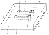
図1は、この発明の実施の形態1における半導体装置を示す斜視図である。図1を参照して、半導体装置は、主表面1aを有する半導体基板1と、駆動することより熱を発生する、主表面1aに形成された図示しない半導体素子と、主表面1a上に形成され、図示しない半導体素子を覆う層間絶縁膜2とを備える。層間絶縁膜2の内部には、冷却路3が形成されている。冷却路3は、層間絶縁膜2の頂面2a上の離れた位置にそれぞれ開口された一方端4および他方端5を有する。冷却路3は、主表面1aに形成された半導体素子の近傍を通過するように、一方端4から他方端5に向けて延びている。
(Embodiment 1)
1 is a perspective view showing a semiconductor device according to
半導体基板1は、たとえばシリコン基板から形成されている。図示しない半導体素子は、代表的には各種のトランジスタ素子であるが、これに限定されず、半導体を利用した素子であればいずれであっても良い。層間絶縁膜2は、たとえば、シリコン酸化膜、PSG(phosphosilicate glass)、BSG(borosilicate glass)、BPSG(borophosphosilicate glass)、TEOS(tetra etyle ortho silicate)およびSOG(スピン・オン・グラス)などから形成されている。また、層間絶縁膜2として、低誘電率材料(Low-k材料)を用いても良い。
The
冷却路3には、一方端4から供給され、他方端5から回収される、半導体素子を冷却するための液体や気体(冷却用流体)が流れる。このような冷却路3に供給される気体としては、窒素ガス、フロンガスならびにヘリウムおよびアルゴンのような不活性ガスを挙げることができる。また、冷却路3を構成する内壁がパッシベーション膜によって被覆され、酸化に対する対策が十分に採られている場合には、乾燥空気を用いることもできる。液体としては、水(純水)やフロンを用いることができる。
A liquid or gas (cooling fluid) for cooling the semiconductor element flows from the one
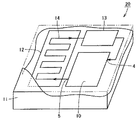
図2は、図1中に示す半導体装置が設けられた半導体パッケージを示す斜視図である。図中では、半導体パッケージの内部を示すため、一部が透視した状態で描かれている。 FIG. 2 is a perspective view showing a semiconductor package provided with the semiconductor device shown in FIG. In the drawing, in order to show the inside of the semiconductor package, a part is drawn through.
図2を参照して、半導体パッケージ20は、図1中に示す半導体装置から構成された半導体チップ10と、ヒートスプレッダ(ヒートシンク)12と、後で詳細に説明するポンプチップ13と、これら部材を覆うパッケージ樹脂11とを備える。ヒートスプレッダ12は、たとえば、銅、鉄−ニッケル合金および半田などから形成されている。
Referring to FIG. 2, a
パッケージ樹脂11の内部には、半導体チップ10に設けられた冷却路3の一方端4および他方端5に両端が接続された冷却路14が形成されている。冷却路14の経路の途中には、相対的に他方端5に近い側に位置して、所定の距離ごとに方向を変えて延びる部分が設けられている。その部分の近傍には、ヒートスプレッダ12が配置されている。冷却路14の経路の途中には、相対的に一方端4に近い側に位置して、ポンプチップ13が設けられている。
Inside the package resin 11, a
図3は、図2中のポンプチップの構造を示す断面図である。図3を参照して、ポンプチップ13は、マイクロマシン技術によってシリコンチップ上に作製されたポンプ構造を備える。そのポンプ構造は、バルブ用シリンダ24およびバルブ用シリンダ24に配置されたバルブ用ピストン25からなるバルブ部26と、ポンプ用シリンダ21およびポンプ用シリンダ21に配置されたポンプ用ピストン22からなるポンプ部23とから構成されている。バルブ用シリンダ24は、流路28によって、他方端5側から延びる冷却路14に接続されている。バルブ用シリンダ24とポンプ用シリンダ21とは、流路27によって互いに接続されている。ポンプ用シリンダ21は、流路29によって、一方端4側から延びる冷却路14に接続されている。
FIG. 3 is a cross-sectional view showing the structure of the pump chip in FIG. Referring to FIG. 3, the
図1から図3を参照して、電極間の静電力を利用した静電アクチュエータ等を用いて、ポンプ用ピストン22およびバルブ用ピストン25を所定の位相差をもって往復運度させ、半導体チップ10に設けられた冷却路3に冷却用流体を循環させる。
With reference to FIGS. 1 to 3, the
ポンプチップ13から冷却路3の一方端4に供給された冷却用流体は、半導体チップ10に設けられた冷却路3を流れる。この際、冷却用流体は、主表面1aに形成された半導体素子から発生する熱を奪い、その後、他方端5側へと回収される。回収された冷却用流体は、ヒートスプレッダ12の近傍を通過する際に、ヒートスプレッダ12へと熱を放出する。その熱は、パッケージ樹脂11を介して半導体パッケージ20の外部へと放熱される。
The cooling fluid supplied from the
なお、冷却用流体を循環させる手段は、図2に示す機構に限定されず、たとえば、パッケージ樹脂11に対して直接、空冷/液冷用の流体を通すチューブを接続し、そのチューブと外部に設けたポンプとをつなぐ機構によっても良い。但し、図2に示すように、ヒートスプレッダ12のみならずポンプチップ13を含んだ冷却系全体をパッケージ樹脂11内に封止すれば、半導体パッケージ20の小型化を図りつつ、半導体チップ10の放熱を効率良く行なうことができる。
The means for circulating the cooling fluid is not limited to the mechanism shown in FIG. 2. For example, a tube through which air / liquid cooling fluid is directly connected is connected to the package resin 11, and the tube and the outside are connected to the outside. A mechanism that connects to the provided pump may be used. However, as shown in FIG. 2, if the entire cooling system including the
この発明の実施の形態1における半導体装置は、主表面1aを有する半導体基板1と、主表面1a上に形成され、主表面1aに設けられた半導体素子を覆う層間絶縁膜2と、層間絶縁膜2に形成され、冷却用流体が流れる第1の冷却路としての冷却路3とを備える。冷却路3は、層間絶縁膜2の内部を循環するように形成されている。冷却路3は、冷却用流体が供給される一方端4と、冷却用流体が排出される他方端5とを含む。
A semiconductor device according to a first embodiment of the present invention includes a
半導体装置としての半導体パッケージ20は、半導体基板1、層間絶縁膜2および冷却路3を含む半導体チップ10と、半導体チップ10を覆うように形成された樹脂部材としてのパッケージ樹脂11と、パッケージ樹脂11内に設けられたポンプ部としてのポンプチップ13および金属材料からなる放熱部としてのヒートスプレッダ12とを備える。ポンプチップ13は、一方端4および他方端5に接続されて、冷却路3に冷却用流体を循環させる。ヒートスプレッダ12は、他方端5から排出された冷却用流体の熱を放熱する。
A
図4から図7は、層間絶縁膜に冷却路を製造する方法の各工程を示す断面図である。図1中に示すトンネル構造を備えた冷却路3は、半導体プロセスにより半導体基板1上に堆積された層間絶縁膜およびメタル配線層の積層構造において、層間絶縁膜の一部を後から除去することによって作製できる。この製造方法について、図4から図7を用いて以下に説明を行なう。
4 to 7 are cross-sectional views showing respective steps of a method for manufacturing a cooling path in an interlayer insulating film. The
図4を参照して、通常の半導体プロセスと同様に、CVD(chemical-vapor deposition)法およびスパッタリング法をそれぞれ用いて、半導体基板1の主表面1a上に、層間絶縁膜31pおよびメタル配線層32pを順次形成する。さらに、メタル配線層32pを覆うように層間絶縁膜31qを形成する。図5を参照して、層間絶縁膜31q上に、メタル配線層32pに達するメタルプラグ35mおよび35nを備えるメタル配線層32qを形成する。このとき、メタルプラグ35mとメタルプラグ35nとの間には、層間絶縁膜33が残存する。メタル配線層32qをパターニングし、互いに距離を隔てた位置に溝34mおよび34nを形成する。
Referring to FIG. 4, similar to a normal semiconductor process, an
図6を参照して、メタル配線層32q上に、溝34mおよび34nを充填する層間絶縁膜31rを形成する。CMP(chemical mechanical polishing)工程により層間絶縁膜31rを平坦化した後、図5に示す工程と同様に、層間絶縁膜31r上に、メタル配線層32qに達するメタルプラグ35mおよび35nを備えるメタル配線層32rを形成する。メタル配線層32rをパターニングし、互いに距離を隔てた位置に溝34mおよび34nを再び形成する。
Referring to FIG. 6,
図7を参照して、図6に示す工程を繰り返し、層間絶縁膜31r上に、所定の形状を有する層間絶縁膜31sおよびメタル配線層32sを順次形成する。その後、フッ酸(HF)を用いたウェットエッチングを実施することによって、メタルプラグ35mとメタルプラグ35nとの間に残された層間絶縁膜33を除去する。以上の工程により、層間絶縁膜とメタル配線層との積層構造に、トンネル構造を有する冷却路37を作製することができる。
Referring to FIG. 7, the process shown in FIG. 6 is repeated, and
なお、図4から図7では、冷却路を層間絶縁膜とメタル配線層との積層構造に作製する場合について説明したが、これに限定されず、たとえば、CVD法によって形成される層間絶縁膜とシリコン膜との積層構造に対しても、同様の製造方法を適用することによって、冷却用流体を流すための冷却路を形成することができる。 4 to 7, the description has been given of the case where the cooling path is formed in a laminated structure of an interlayer insulating film and a metal wiring layer. However, the present invention is not limited to this. For example, an interlayer insulating film formed by a CVD method and By applying the same manufacturing method to the laminated structure with the silicon film, a cooling path for flowing a cooling fluid can be formed.
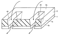
図8は、図1中に示す半導体装置の変形例を示す斜視図である。図中には、半導体装置の断面が示されている。図8を参照して、本変形例では、図1中に示す冷却路として、層間絶縁膜2の頂面2a側から半導体基板1の裏面1b側にまで達するビアホール41が形成されている。ビアホール41は、主表面1aに平行な平面で切断された断面の面積が、頂面2aから裏面1bに向かうに従って小さくなるように形成されている。
FIG. 8 is a perspective view showing a modification of the semiconductor device shown in FIG. In the drawing, a cross section of the semiconductor device is shown. Referring to FIG. 8, in this modification, a via
図9は、図1中に示す半導体装置の別の変形例を示す斜視図である。図中には、半導体装置の断面が示されている。図9を参照して、本変形例では、図1中に示す冷却路として、層間絶縁膜2の頂面2a側から半導体基板1の裏面1b側にまで達するビアホール42が形成されている。ビアホール42は、主表面1aに平行な平面で切断された断面の面積が、頂面2aから裏面1bに向かうに従って大きくなるように形成されている。なお、図8および図9中には図示しなかったが、これらの変形例では、ビアホール41および42から延びる冷却用流体を循環、通過させるための流路が、半導体基板1の裏面1b側を覆うパッケージ樹脂により構成されている。
FIG. 9 is a perspective view showing another modification of the semiconductor device shown in FIG. In the drawing, a cross section of the semiconductor device is shown. Referring to FIG. 9, in the present modification, a via
このように構成された半導体装置によれば、設けた冷却路に冷却用流体を流すことによって、主表面1a上の半導体素子から発生した熱を半導体装置の外部に効率良く放熱することができる。これにより、半導体素子を熱の影響から保護し、所望の半導体特性を得ることができる。また、発熱による温度上昇から決定されるような半導体チップの動作周波数や回路の処理性能の上限を小さくし、より高性能な半導体集積回路を実現することができる。
According to the semiconductor device configured as described above, by flowing the cooling fluid through the provided cooling path, the heat generated from the semiconductor element on the
加えて、冷却路3を層間絶縁膜2の内部に形成することにより、狭い領域への冷却路の配置が可能となる。これにより、発熱体である半導体素子の近傍に冷却路3を設けやすくなる。また、冷却路3は、冷却用流体が供給され回収される一方端4および他方端5を有し、パッケージ樹脂11の内部には、一方端4と他方端5との間に位置して、冷却用流体から熱を奪うヒートスプレッダ12が配置されている。このため、冷却路3には、温度が低くされた冷却用流体が次々と供給される。これにより、さらに効率の良い放熱を行なうことができる。
In addition, by forming the
(実施の形態2)
図10は、この発明の実施の形態2における半導体装置の一部を示す断面図である。本実施の形態における半導体装置は、実施の形態1に記載の半導体装置が備える冷却構造に加えて、図10を用いて説明する冷却構造をさらに備える。なお図中において、実施の形態1に記載の半導体装置と比較して、同一またはそれに相当する部材には、同じ参照番号を付している。
(Embodiment 2)
FIG. 10 is a sectional view showing a part of the semiconductor device according to the second embodiment of the present invention. The semiconductor device in this embodiment further includes a cooling structure described with reference to FIG. 10 in addition to the cooling structure included in the semiconductor device described in
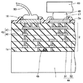
図10を参照して、半導体基板1の主表面1aには、半導体素子としてのトランジスタ素子45が形成されている。主表面1a上には、トランジスタ素子45を覆うように層間絶縁膜2が多層に堆積されている。層間絶縁膜2には、トランジスタ素子45に接続され、電気信号配線や電源配線として実際に機能する配線43が形成されている。配線43は、層間絶縁膜2の各層に設けられた、メタル配線46と、メタル配線46に接続されたビア配線47とから構成されている。層間絶縁膜2の各層に設けられたこれらメタル配線46およびビア配線47は、層間絶縁膜2の多層間に連なって形成されている。層間絶縁膜2の最上層に形成されたビア配線47は、層間絶縁膜2の頂面2aから露出するように形成されている。その露出するビア配線47に接触するようにボンディングパッド16が形成されている。ボンディングパッド16には、ボンディングワイヤ50が接続されている。
Referring to FIG. 10,
層間絶縁膜2には、信号・電源の電流容量として必要十分な配線43に加えて、冷却を目的とした配線44が形成されている。配線44は、配線43と同様に、層間絶縁膜2の多層間に連なるメタル配線51およびビア配線52から構成されている。頂面2aから露出するビア配線52に接触するように、メタルパッド17が形成されている。層間絶縁膜2の頂面2aから隙間を隔てた位置には、メタルバンプ48を介してメタルパッド17に接続されたヒートスプレッダ49が設けられている。
In the
トランジスタ素子45は、配線43と配線44との間に配置されている。配線43および配線44は、たとえば、銅、アルミニウム、チタン、タングステン、コバルトおよびタンタルなどの金属、これらの合金、これらにシリコンを添加した材料ならびにシリサイドなどから形成することができる。これらの材料は、層間絶縁膜2を形成するシリコン酸化膜などの材料と比較して、熱伝導率が大きい。
The
なお、配線43および配線44を構成するメタル配線には、特にアルミニウムおよび銅を主成分とする材料が用いられ、ビア配線には、特にタングステンや銅が用いられる。また、コバルトやチタンのような金属は、シリコンとの界面にシリサイドを形成したサリサイド配線や、バリアメタルとして設けられた配線層の下層膜として用いられる。
In addition, a material mainly composed of aluminum and copper is used for the metal wiring constituting the
この発明の実施の形態2における半導体装置は、層間絶縁膜2に形成され、層間絶縁膜2の熱伝導率に対して相対的に大きい熱伝導率を有する第1の放熱部材としての配線43および配線44をさらに備える。配線43および配線44は、ビア配線47および52と金属配線としてのメタル配線46および51とを含む。配線43および配線44は、層間絶縁膜2の表面としての頂面2aから露出している。半導体装置は、層間絶縁膜2の外部に配置され、層間絶縁膜2の頂面2aから露出する配線43および配線44に接続された第2の放熱部材としてのヒートスプレッダ49をさらに備える。
The semiconductor device according to the second embodiment of the present invention is formed in
このように構成された半導体装置によれば、層間絶縁膜2と比較して熱伝導率が大きい配線43および配線44を、層間絶縁膜2内で冷却構造として機能させることができる。これにより、トランジスタ素子45から発生した熱を効率良く放熱することができる。また、配線43および配線44は、頂面2a上に露出するように形成されているため、熱が層間絶縁膜2内にこもるということがない。加えて、配線44は、頂面2a上においてヒートスプレッダ49に接続されているため、配線44を介して頂面2a上にまで伝わった熱を、さらに外部へと効率良く放熱することができる。
According to the semiconductor device configured as described above, the
なお、電気・信号配線や電源配線として設けられたものの実際には使用されていない配線の全てまたは一部を、上述の放熱構造として利用しても良い。 Note that all or a part of the wirings that are provided as electric / signal wirings and power supply wirings but are not actually used may be used as the above-described heat dissipation structure.
図11は、図10中に示す半導体装置の変形例を示す断面図である。図11を参照して、本変形例では、層間絶縁膜2に、頂面2a側に開口するトレンチ56が形成されている。トレンチ56の表面は、メタル配線膜57によって覆われている。トレンチ56の内部は、めっきにより形成され、たとえば銅などからなる放熱部材58によって充填されている。層間絶縁膜2の頂面2a上では、頂面2aから突出した位置に延在する放熱部材58の頂面とヒートスプレッダ49とが接続されている。図12は、図10中に示す半導体装置の別の変形例を示す断面図である。図12を参照して、本変形例では、図11中に示す冷却構造に対して、放熱部材58とヒートスプレッダ49との間にメタルバンプ48が介在している。
FIG. 11 is a cross-sectional view showing a modification of the semiconductor device shown in FIG. Referring to FIG. 11, in the present modification,
これらの構成によっても、図10中に示す半導体装置で得られる効果と同様の効果を得ることができる。なお、図11および図12に示すトレンチ56は、層間絶縁膜2の頂面2a側から半導体基板1の裏面1b側にまで達するように形成されていても良い。
Also with these configurations, the same effects as those obtained with the semiconductor device shown in FIG. 10 can be obtained. The
(実施の形態3)
図13は、この発明の実施の形態3における半導体装置の一部を示す断面図である。本実施の形態における半導体装置は、実施の形態1に記載の半導体装置が備える冷却構造に加えて、図13を用いて説明する冷却構造をさらに備える。なお図中において、既に説明した半導体装置と比較して、同一またはそれに相当する部材には、同じ参照番号を付している。
(Embodiment 3)
FIG. 13 is a cross-sectional view showing a part of the semiconductor device according to the third embodiment of the present invention. The semiconductor device in this embodiment further includes a cooling structure described with reference to FIG. 13 in addition to the cooling structure included in the semiconductor device described in
図13を参照して、層間絶縁膜2には、実施の形態2における配線43または配線44に対応する配線66、67、68および69が所定の間隔を隔てて形成されている。層間絶縁膜2には、さらに、配線66、67および68のそれぞれの間に位置して、頂面2a側に開口するトレンチ63が形成されている。トレンチ63は、たとえば銅などからなる放熱部材64によって充填されている。放熱部材64は、層間絶縁膜2の頂面2a上に形成されたメタルパッド17に接触している。層間絶縁膜2には、さらに、メタル配線68および69の間に位置して、頂面2a側に開口するトレンチ62が形成されている。トレンチ62の内部には、冷却用の液体が通過、循環される。
Referring to FIG. 13, wirings 66, 67, 68 and 69 corresponding to wiring 43 or
このようなトレンチは、半導体ウェハの製造工程において通常利用されるドライエッチング工程により形成することができる。また、さらに大口径の開口を形成したい場合には、たとえば、水酸化カリウム溶液(KOH)を用いたシリコン基板の異方性ウェットエッチングを適用することによって、パターン形状に基づく四角錐状の孔を形成することができる。 Such a trench can be formed by a dry etching process normally used in a semiconductor wafer manufacturing process. Further, when it is desired to form an opening having a larger diameter, for example, by applying anisotropic wet etching of a silicon substrate using a potassium hydroxide solution (KOH), a quadrangular pyramidal hole based on the pattern shape is formed. Can be formed.
このように構成された半導体装置によれば、層間絶縁膜2に形成された配線66から69に加えて、トレンチ63を充填する放熱部材64およびトレンチ62を流れる冷却用の液体が冷却のために機能する。このため、放熱の効率をさらに向上させることができる。
According to the semiconductor device configured as described above, in addition to the
(実施の形態4)
図14は、この発明の実施の形態4における半導体装置を示す斜視図である。本実施の形態における半導体装置は、実施の形態1に記載の半導体装置が備える冷却構造に加えて、図14を用いて説明する冷却構造をさらに備える。なお図中において、既に説明した半導体装置と比較して、同一またはそれに相当する部材には、同じ参照番号を付している。
(Embodiment 4)
FIG. 14 is a perspective view showing a semiconductor device according to the fourth embodiment of the present invention. The semiconductor device in this embodiment further includes a cooling structure described with reference to FIG. 14 in addition to the cooling structure included in the semiconductor device described in
図14を参照して、本実施の形態における半導体装置は、高周波集積回路を構成している。層間絶縁膜2の頂面2a上には、L字状に折れ曲がって延びるインダクタ74と、渦巻き状に折れ曲がって延びるアンテナ73とが形成されている。インダクタ74およびアンテナ73は、たとえば、アルミニウムや銅を主成分とする材料から形成されている。主表面1aには、半導体素子71および72が形成されている。層間絶縁膜2には、半導体素子71および72に接続されたメタル配線46およびビア配線47からなる配線43が形成されている。インダクタ74およびアンテナ73は、配線43に接続されている。
Referring to FIG. 14, the semiconductor device in the present embodiment forms a high-frequency integrated circuit. On the
この発明の実施の形態4における半導体装置では、第2の放熱部材は、インダクタ素子としてのインダクタ74およびアンテナ素子としてのアンテナ73の少なくともいずれか一方を含む。
In the semiconductor device according to the fourth embodiment of the present invention, the second heat radiating member includes at least one of an
このように構成された半導体装置によれば、配線43に加えて、インダクタ74およびアンテナ73を冷却構造として機能させることができる。このため、配線43を介して層間絶縁膜2の頂面2a上にまで伝わった熱を、さらに外部へと効率良く放熱することができる。
According to the semiconductor device configured as described above, in addition to the
(実施の形態5)
図15は、この発明の実施の形態5における半導体装置を示す斜視図である。図中には、半導体装置の断面が示されている。本実施の形態における半導体装置は、実施の形態1に記載の半導体装置が備える冷却構造に加えて、図15を用いて説明する断熱構造をさらに備える。なお図中において、既に説明した半導体装置と比較して、同一またはそれに相当する部材には、同じ参照番号を付している。
(Embodiment 5)
FIG. 15 is a perspective view showing a semiconductor device according to the fifth embodiment of the present invention. In the drawing, a cross section of the semiconductor device is shown. The semiconductor device in this embodiment further includes a heat insulating structure described with reference to FIG. 15 in addition to the cooling structure included in the semiconductor device described in
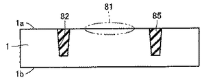
図15を参照して、半導体基板1の主表面1aには、半導体素子81が形成されている。半導体基板1には、主表面1a側に開口し、半導体素子81を取り囲むように延在するトレンチ82が形成されている。トレンチ82は、たとえばシリコン酸化膜やシリコン窒化膜からなる断熱部材85によって充填されている。これら断熱部材85を構成する材料は、半導体基板1を構成するシリコン等と比較して、小さい熱伝導率を有する。
Referring to FIG. 15,
半導体素子81は、熱の影響を小さく抑えたい半導体素子、たとえばアナログ回路を構成する半導体素子である。断熱部材85を挟んで半導体素子81の周囲に発熱量の大きい半導体素子が形成されている場合、その半導体素子から発生した熱が、半導体素子81に伝わることを抑制できる。これにより、半導体素子81に流れる電流値が、温度変化によって大きく変動することを防止できる。
The
また、断熱部材85に囲まれた領域に、半導体素子81と発熱量の大きい半導体素子とを形成しても良い。この場合、断熱部材85に囲まれた領域の外側に形成された半導体素子からの熱を遮断し、断熱部材85に囲まれた領域内を恒温化することができる。これによっても、上述の効果と同様の効果を得ることができる。
Further, the
この発明の実施の形態5における半導体装置では、半導体基板1には、半導体素子81を取り囲むように、主表面1a側に開口する凹部としてのトレンチ82が形成されている。
In the semiconductor device according to the fifth embodiment of the present invention, a
図16は、図15中に示す半導体装置の変形例を示す斜視図である。図17は、図16中のXVII−XVII線上に沿った断面図である。図16および図17を参照して、本変形例では、L字状に折れ曲がった形状を有する2つのトレンチ82が、半導体素子81を挟んで互いに対峙する位置に形成されている。このように、半導体基板1に形成するトレンチは、半導体素子81を完全に取り囲むように形成されていなくても良い。
FIG. 16 is a perspective view showing a modification of the semiconductor device shown in FIG. 17 is a cross-sectional view taken along the line XVII-XVII in FIG. Referring to FIGS. 16 and 17, in the present modification, two
図18は、図15中に示す半導体装置の別の変形例を示す斜視図である。図19は、図18中のXIX−XIX線上に沿った断面図である。図18および図19を参照して、本変形例では、半導体基板1には、主表面1a上において一方向に延び、半導体基板1の主表面1a側から裏面1b側にまで達する4つのトレンチ87が形成されている。4つのトレンチ87は、半導体素子81を取り囲む四辺にそれぞれ配置されている。このようなトレンチ87を形成し、半導体素子81とその周りとを切り離すことによっても、上述の効果と同様の効果を得ることができる。なお、トレンチ87に、冷却用の流体を注入したり充填したりしても良い。
FIG. 18 is a perspective view showing another modification of the semiconductor device shown in FIG. FIG. 19 is a cross-sectional view along the line XIX-XIX in FIG. Referring to FIGS. 18 and 19, in this modification, the
このように構成された半導体装置によれば、半導体基板1において局所的に発生する熱変化が、その影響を受けやすい半導体素子81に及ぶことを抑制できる。
According to the semiconductor device configured as described above, it is possible to suppress a heat change locally generated in the
(実施の形態6)
図20は、この発明の実施の形態6における半導体装置の一部を示す断面図である。本実施の形態における半導体装置は、実施の形態1に記載の半導体装置が備える冷却構造に加えて、図20を用いて説明する冷却構造をさらに備える。なお図中において、既に説明した半導体装置と比較して、同一またはそれに相当する部材には、同じ参照番号を付している。
(Embodiment 6)
FIG. 20 is a cross sectional view showing a part of the semiconductor device according to the sixth embodiment of the present invention. The semiconductor device in this embodiment further includes a cooling structure described with reference to FIG. 20 in addition to the cooling structure included in the semiconductor device described in
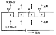
図20を参照して、半導体基板1の主表面1aには、半導体素子90が形成されている。主表面1a上には、複数の層2pから2sが積層されてなる層間絶縁膜2が形成されている。層間絶縁膜2には、メタル配線51およびビア配線52からなる配線44が形成されている。層間絶縁膜2には、さらに、層2qに位置して、2種の異なる金属(アルミニウム、銅、タングステン、チタンおよびコバルトなど)または異なる導電型の半導体(シリコンおよびゲルマニウムなど)からなるペルチェ素子92および93が、主表面1aに平行な方向に交互に並んで形成されている。層2rに形成されたメタル配線51と層2qに形成されたメタル配線51とが交互になって、ペルチェ素子92および93を、隣り合う位置において互いに接続している。層間絶縁膜2の頂面2a上には、ヒートスプレッダ49が設けられている。ヒートスプレッダ49とビア配線52に接触するメタルパッド17とが、メタルバンプ48を介して接続されている。
Referring to FIG. 20,
図21は、図20に示す半導体装置で得られるペルチェ(peltier)効果を説明するための説明図である。図20および図21を参照して、ペルチェ素子92および93が、それぞれn型シリコンおよびp型シリコンから形成されており、図中に示す方向に電流を流す場合を想定する。この場合、電流がペルチェ素子92からペルチェ素子93に向かう側で吸熱作用が生じ、電流がペルチェ素子93からペルチェ素子92に向かう側で放熱作用が生じる。結果、主表面1aに形成された半導体素子90で発生した熱は、ペルチェ素子92および93が設けられた位置へと吸熱され、さらに、層間絶縁膜2の頂面2aへと放熱される。その熱は、メタルバンプ48を介してヒートスプレッダ49から外部へと放熱される。
FIG. 21 is an explanatory diagram for explaining the Peltier effect obtained in the semiconductor device shown in FIG. Referring to FIGS. 20 and 21, it is assumed that
この発明の実施の形態6における半導体装置は、層間絶縁膜2に形成されたペルチェ素子92および93をさらに備える。
The semiconductor device according to the sixth embodiment of the present invention further includes
このように構成された半導体装置によれば、ペルチェ素子92および93に所定の方向の電流を流し、ペルチェ効果を得ることによって、特定部位(本実施の形態では、主表面1a上の半導体素子90)を冷却することができる。これにより、配線44による効果に加えて、放熱の効率をさらに向上させることができる。
According to the semiconductor device configured as described above, a current in a predetermined direction is supplied to the
(実施の形態7)
図22は、この発明の実施の形態7における半導体装置を示す斜視図である。図23は、図22中のXXIII−XXIII線上に沿った断面図である。本実施の形態における半導体装置は、実施の形態1に記載の半導体装置が備える冷却構造に加えて、図22を用いて説明する冷却構造をさらに備える。
(Embodiment 7)
FIG. 22 is a perspective view showing a semiconductor device according to the seventh embodiment of the present invention. 23 is a cross-sectional view taken along line XXIII-XXIII in FIG. The semiconductor device in this embodiment further includes a cooling structure described with reference to FIG. 22 in addition to the cooling structure included in the semiconductor device described in
図22および図23を参照して、半導体パッケージ101は、図1中に示す半導体装置から構成された半導体チップ10と、半導体チップ10と所定の間隔を隔てて配置されたヒートスプレッダ104と、半導体チップ10およびヒートスプレッダ104を覆うパッケージ樹脂110とを備える。パッケージ樹脂110の内部には、冷却用流体が供給される一方端106と冷却用流体が回収される他方端107とを有する冷却路105が形成されている。冷却路105は、ヒートスプレッダ104の近傍において、所定の距離ごとに方向を変えながら一方端106から他方端107に向けて延びている。
Referring to FIGS. 22 and 23, a
この発明の実施の形態7における半導体装置としての半導体パッケージ101は、半導体基板1、層間絶縁膜2および冷却路3を含む半導体チップ10と、半導体チップ10を覆うように形成された樹脂部材としてのパッケージ樹脂110と、パッケージ樹脂110に形成され、冷却用流体が流れる第2の冷却路としての冷却路105とを備える。
A
このように構成された半導体パッケージ101によれば、半導体チップ10に設けられた冷却構造によりチップ外に放出された熱は、パッケージ樹脂110を介してヒートスプレッダ104へと伝わる。本実施の形態では、ヒートスプレッダ104に近接して冷却路105が形成されているため、冷却路105を流れる冷却用流体を通じて、チップ外に放出された熱を、さらにパッケージ外へと効率良く放熱することができる。
According to the
(実施の形態8)
図24は、この発明の実施の形態8における半導体装置を示す断面図である。本実施の形態における半導体装置は、実施の形態1に記載の半導体装置が備える冷却構造に加えて、図24を用いて説明する冷却構造をさらに備える。
(Embodiment 8)
24 is a cross sectional view showing a semiconductor device according to the eighth embodiment of the present invention. The semiconductor device in this embodiment further includes a cooling structure described with reference to FIG. 24 in addition to the cooling structure included in the semiconductor device described in
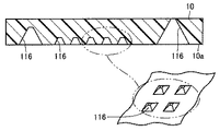
図24を参照して、図1中に示す半導体装置から構成された半導体チップ10は、複数の四角錐状の孔116が形成された表面10aを有する。孔116は、その底面がチップ内に形成されていたり、貫通していたりする。このような孔116により、半導体チップ10の表面10aは凹凸形状に形成されている。
Referring to FIG. 24,
この発明の実施の形態8における半導体チップ10では、半導体チップ10の表面10aが凹凸形状に形成されている。
In the
このように構成された半導体チップ10によれば、表面10aの表面積を増大させることができる。これにより、半導体チップ10の内部に配置された半導体素子で発生する熱を効率良くチップ外へと放熱することができる。
According to the
図25は、図24中に示す半導体装置の変形例を示す断面図である。図25を参照して、本変形例では、半導体チップ10の表面10aが、機械的に粗く研磨されることによって、凹凸形状に粗面化されている。半導体チップ10には、その粗面化された表面10aに接触するように、たとえば、銅、鉄−ニッケル合金および半田などからなる放熱部材121が設けられている。このような構成により、放熱部材121と半導体チップ10との接触面積を増大させ、効率の良い放熱を実現することができる。
FIG. 25 is a cross-sectional view showing a modification of the semiconductor device shown in FIG. Referring to FIG. 25, in this modification, the
また別の変形例として、半導体チップを作製する半導体プロセスにおいて、ゲート電極用として堆積したポリシリコン膜の一部の領域に、HSG(hemispherical silicon grain)酸化工程を実施しても良い。この場合、堆積したポリシリコン膜上に、さらにアモルファス(非晶質)シリコン薄膜を堆積する。その後、550℃程度の温度で熱処理し、ポリシリコン膜上に粒状のシリコンを成長させる。これらの工程により、ポリシリコン膜の表面に半球状の凹凸形状を形成することができる。 As another modification, in a semiconductor process for manufacturing a semiconductor chip, an HSG (hemispherical silicon grain) oxidation step may be performed on a partial region of the polysilicon film deposited for the gate electrode. In this case, an amorphous (amorphous) silicon thin film is further deposited on the deposited polysilicon film. Thereafter, heat treatment is performed at a temperature of about 550 ° C. to grow granular silicon on the polysilicon film. Through these steps, a hemispherical uneven shape can be formed on the surface of the polysilicon film.
(実施の形態9)
図26は、この発明の実施の形態9における半導体装置を示す断面図である。図29を参照して、半導体パッケージ131は、複数の半導体チップ132が内部に搭載されるマルチチップタイプの半導体パッケージである。半導体パッケージ131は、互いに所定の間隔を隔てて位置決めされた複数の半導体チップ132(132a、132bおよび132c)と、複数の半導体チップ132の間を接続するメタルバンプ133と、複数の半導体チップ132の間に配置された、たとえば銅などからなる放熱部材135とを備える。なお図示しないが、半導体パッケージ131には、複数の半導体チップ132間のフィラーとして、パッケージ樹脂やポリイミドなどの樹脂材料が設けられている。
(Embodiment 9)
FIG. 26 is a sectional view showing a semiconductor device according to the ninth embodiment of the present invention. Referring to FIG. 29, a
複数の半導体チップ132は、半導体チップ132aおよび132cが両端に位置し、半導体チップ132bがその間に位置するように配置されている。複数の半導体チップ132の各々には、チップを貫通するビア配線134が形成されている。メタルバンプ133がそのビア配線134に接触して設けられることによって、複数の半導体チップ132が積層された状態で互いに接続されている。
The plurality of
半導体チップ132cに隣り合う位置には、半導体チップ132cとの間に間隔を設けてヒートスプレッダ136が配置されている。半導体チップ132cとヒートスプレッダ136とは、半導体チップ132cに形成されたビア配線134に接触するメタルバンプ133によって接続されている。半導体チップ132cとヒートスプレッダ136との間には、放熱部材135が配置されている。
A
なお、本実施の形態では、複数の半導体チップ132の間および半導体チップ132cとヒートスプレッダ136との間に放熱部材135を配置したが、本発明は、これに限定されない。たとえば、これらの間を充填するパッケージ樹脂に冷却路を形成し、その冷却路に冷却用の気体や液体を流しても良い。
In the present embodiment, the
また、本実施の形態では、駆動させた場合の発熱が比較的小さい半導体チップ132bが、複数の半導体チップ132の配列の中間部分に位置決めされ、発熱が比較的大きい半導体チップ132aおよび132cが、複数の半導体チップ132の配列の両端に配置されている。また好ましくは、半導体チップ132aおよび132bの発熱量が、ヒートスプレッダ136に隣り合って設けられた半導体チップ132cの発熱量よりも小さくても良い。
In the present embodiment, the
この発明の実施の形態9におけるマルチチップタイプの半導体パッケージ131は、互いに間隔を隔てて一方向に配列された複数の半導体チップ132と、複数の半導体チップ132の各々に直接、接触し、隣り合う複数の半導体チップ132を互いに接続する金属配線としてのメタルバンプ133と、隣り合う複数の半導体チップ132間に配置された放熱手段としての放熱部材135とを備える。一方向に配列された複数の半導体チップ132のうち中間に位置する半導体チップ132bから発生する熱量が、一方向に配列された複数の半導体チップ132のうち両端に位置する半導体チップ132aおよび132cから発生する熱量よりも小さい。
A multi-chip
半導体パッケージ131は、一方向に配列された複数の半導体チップ132のうち端に位置する半導体チップ132cに隣り合い、半導体チップ132cに接続された放熱板としてのヒートスプレッダ136をさらに備える。ヒートスプレッダ136が接続された半導体チップ132cを除く他の複数の半導体チップ132aおよび132bから発生する熱量は、ヒートスプレッダ136が接続された半導体チップ132cから発生する熱量よりも小さい。
The
このように構成された半導体パッケージ131によれば、複数の半導体チップ132は、互いにメタルバンプ133を介して接続されているため、発生した熱をチップ間で熱伝導させることができる。これにより、複数の半導体チップ132を配列した方向の温度勾配を低減させるとともに、チップ間に配置した放熱部材135および半導体チップ132cに隣り合って配置したヒートスプレッダ136によって、複数の半導体チップ132を冷却することができる。
According to the
一般的に、半導体チップには、ジャンクション温度の絶対最大定格が設けられており、素子破壊を起こさないための温度上限が存在する。また、半導体素子を高温で動作させると、半導体内部のキャリア移動度の低下に伴うトランジスタ性能の劣化、ドライバの駆動電流/ドライバ能力の低下および動作速度の低下、ならびに接合リーク電流の急激な上昇による消費電力の増大など、デバイス特性の劣化が引き起こされる。また、チップ間に温度勾配が存在すると、半導体特性のばらつきが増大し、設計上の動作タイミングに対してずれが生じることも想定される。特に、信号の送信側と受信側とで温度が異なり、信号タイミングにずれが生じた場合は、誤動作を引き起こす可能性がある。本実施の形態における半導体パッケージ131によれば、上述の効果によりこれらの問題を解決することができる。
In general, a semiconductor chip is provided with an absolute maximum rating of a junction temperature, and there is an upper temperature limit for preventing element destruction. In addition, when a semiconductor element is operated at a high temperature, the transistor performance deteriorates due to a decrease in carrier mobility inside the semiconductor, the driver drive current / driver ability decreases and the operation speed decreases, and the junction leakage current rapidly increases. Deterioration of device characteristics such as an increase in power consumption is caused. In addition, if there is a temperature gradient between chips, it is assumed that variations in semiconductor characteristics increase and a deviation from the design operation timing occurs. In particular, if the signal transmission side and the reception side have different temperatures and a signal timing shifts, malfunction may occur. According to the
また、複数の半導体チップ132が配列された中間部分やヒートスプレッダ136から離れた位置では、半導体チップから発生した熱が比較的、放熱されにくい。このため、このような位置に発熱量の大きい半導体チップを配置することによって、温度勾配をさらに低減させ、半導体チップをさらに効率良く冷却することができる。
Further, heat generated from the semiconductor chip is relatively difficult to dissipate at an intermediate portion where the plurality of
(実施の形態10)
図27は、この発明の実施の形態10における半導体装置を示す斜視図である。図28は、図27中に示す矢印XXVIIIから見た半導体装置を示す正面図である。
(Embodiment 10)
FIG. 27 is a perspective view showing a semiconductor device according to the tenth embodiment of the present invention. FIG. 28 is a front view showing the semiconductor device as viewed from an arrow XXVIII shown in FIG.
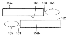
図27および図28を参照して、半導体パッケージ151は、複数の半導体チップ152が内部に搭載されるマルチチップタイプの半導体パッケージである。半導体パッケージ151は、間隔を隔てて位置決めされた複数の半導体チップ152(152a、152bおよび152c)と、複数の半導体チップ152間を充填し、パッケージ樹脂やポリイミドなどからなる図示しない樹脂材料と、その樹脂材料に形成され、冷却用の気体や液体が流される冷却路155とを備える。
27 and 28,
半導体チップ152aおよび152cは、互いに向い合う位置において、表面161および163をそれぞれ有する。半導体チップ152bは、半導体チップ152cと向い合う位置において表面162を有する。半導体チップ152aおよび152cは、表面161に表面163と向い合わない部分が生じるように、互いにずれて配置されている。表面163と向い合わない表面161のその部分の近傍には、半導体チップ152aおよび152cに隣り合って、空間153が規定されている。同様に、半導体チップ152bは、半導体チップ152cの表面163と向い合わない部分を表面162に有し、その部分の近傍には、半導体チップ152bおよび152cに隣り合って、空間153が規定されている。さらに、半導体チップ152aと半導体チップ152bとの間にも、空間153が規定されている。
The
冷却路155は、その空間153に位置し、半導体チップの周縁に沿って延びている。なお、冷却路155のほか、銅などからなる放熱部材を空間153に配置しても良い。
The
図29は、図28中に示す半導体パッケージの変形例を示す正面図である。図29を参照して、本変形例では、半導体チップ152bおよび152cが、図28中に示す半導体パッケージ151と同様に配置されている。半導体チップ152bおよび152cに隣り合って規定された空間153には、冷却路155が設けられている。
FIG. 29 is a front view showing a modification of the semiconductor package shown in FIG. Referring to FIG. 29, in this modification,
図30は、図28中に示す半導体パッケージの別の変形例を示す正面図である。図30を参照して、半導体パッケージは、互いに所定の間隔を隔てて位置決めされた複数の半導体チップ152(152dおよび152e)と、複数の半導体チップ152間を充填し、パッケージ樹脂やポリイミドなどからなる図示しない樹脂材料と、その樹脂材料に形成され、冷却用の気体や液体が流される冷却路155とを備える。
FIG. 30 is a front view showing another modification of the semiconductor package shown in FIG. Referring to FIG. 30, the semiconductor package is filled with a plurality of semiconductor chips 152 (152d and 152e) positioned at a predetermined interval and a plurality of
半導体チップ152dおよび152eは、互いに向い合う位置において、表面181および182をそれぞれ有する。表面182は、表面181より大きい面積で形成されており、表面181と向い合わない部分を有する。表面181と向い合わない表面182のその部分の近傍には、半導体チップ152dおよび152eに隣り合って、空間153が規定されている。冷却路155は、その空間153に位置し、半導体チップ152dの周縁に沿って延びている。
The
この発明の実施の形態10におけるマルチチップタイプの半導体パッケージ151は、互いに隣り合う位置に空間153を規定するように配置された複数の半導体チップ152と、空間153に設けられた放熱手段としての冷却路155とを備える。複数の半導体チップ152は、互いに向い合う位置において異なる大きさの表面181および182を有する2つの半導体チップ152dおよび152eと、隣り合った位置においてずれて配置された2つの半導体チップ152aおよび152c(152bおよび152c)との少なくともいずれか一方を含む。放熱手段は、冷却用流体が流れる冷却路155および金属材料からなる放熱部材の少なくともいずれか一方を含む。
A multi-chip
このように構成された半導体パッケージ151によれば、隣り合う半導体チップ間に規定された空間153に冷却路155を形成しているため、半導体パッケージ151をコンパクトに維持しつつ、半導体チップを効率良く冷却することができる。これにより、半導体パッケージ151に搭載する半導体チップの数を増大させることができ、高性能な半導体集積回路を実現することができる。
According to the
なお、以上に説明した実施の形態1から10の半導体装置を適宜、組み合わせて、半導体装置を構成しても良い。この場合、組み合わせた実施の形態の半導体装置で得られる効果を総合的に得ることができる。 The semiconductor device may be configured by appropriately combining the semiconductor devices of the first to tenth embodiments described above. In this case, the effects obtained by the combined semiconductor devices of the embodiments can be obtained comprehensively.
今回開示された実施の形態はすべての点で例示であって制限的なものではないと考えられるべきである。本発明の範囲は上記した説明ではなくて特許請求の範囲によって示され、特許請求の範囲と均等の意味および範囲内でのすべての変更が含まれることが意図される。 The embodiment disclosed this time should be considered as illustrative in all points and not restrictive. The scope of the present invention is defined by the terms of the claims, rather than the description above, and is intended to include any modifications within the scope and meaning equivalent to the terms of the claims.
1 半導体基板、1a 主表面、2 層間絶縁膜、2a 頂面、3,105,155 冷却路、4 一方端、5 他方端、10,132,132a,132b,132c,152,152a,152b,152c,152d,152e 半導体チップ、10a,181,182 表面、11,110 パッケージ樹脂、12,49,136 ヒートスプレッダ、13 ポンプチップ、20,131,151 半導体パッケージ、43,44,66,67,68,69 配線、46,51 メタル配線、47,52 ビア配線、64,135 放熱部材、73 アンテナ、74 インダクタ、81 半導体素子、82,87 トレンチ、92,93 ペルチェ素子、133 メタルバンプ、153 空間。
DESCRIPTION OF
Claims (1)
前記半導体基板の前記主表面に形成される半導体素子と、
前記半導体基板の前記主表面上に形成され、前記半導体素子を覆うように設けられる層間絶縁膜と、
前記層間絶縁膜に形成され、冷却用流体を流すための冷却路とを備え、
前記冷却路は、前記層間絶縁膜の内部を循環するように形成され、
前記冷却路は、冷却用流体が供給される一方端と、冷却用流体が排出される他方端とを含み、さらに、
前記層間絶縁膜の内部に形成される多層のメタル配線層を備え、
前記冷却路は、前記多層のメタル配線層をパターニングすることによって形成された溝で構成される、半導体装置。 A semiconductor substrate having a main surface;
A semiconductor element formed on the main surface of the semiconductor substrate;
An interlayer insulating film formed on the main surface of the semiconductor substrate and provided to cover the semiconductor element;
A cooling path for flowing a cooling fluid, formed in the interlayer insulating film,
The cooling path is formed to circulate inside the interlayer insulating film ,
The cooling path includes one end to which a cooling fluid is supplied and the other end from which the cooling fluid is discharged, and
A multilayer metal wiring layer formed inside the interlayer insulating film;
The said cooling path is a semiconductor device comprised by the groove | channel formed by patterning the said multilayer metal wiring layer .
Priority Applications (1)
| Application Number | Priority Date | Filing Date | Title |
|---|---|---|---|
| JP2004111380A JP4458906B2 (en) | 2004-04-05 | 2004-04-05 | Semiconductor device |
Applications Claiming Priority (1)
| Application Number | Priority Date | Filing Date | Title |
|---|---|---|---|
| JP2004111380A JP4458906B2 (en) | 2004-04-05 | 2004-04-05 | Semiconductor device |
Publications (3)
| Publication Number | Publication Date |
|---|---|
| JP2005294760A JP2005294760A (en) | 2005-10-20 |
| JP2005294760A5 JP2005294760A5 (en) | 2007-05-10 |
| JP4458906B2 true JP4458906B2 (en) | 2010-04-28 |
Family
ID=35327313
Family Applications (1)
| Application Number | Title | Priority Date | Filing Date |
|---|---|---|---|
| JP2004111380A Expired - Fee Related JP4458906B2 (en) | 2004-04-05 | 2004-04-05 | Semiconductor device |
Country Status (1)
| Country | Link |
|---|---|
| JP (1) | JP4458906B2 (en) |
Families Citing this family (11)
| Publication number | Priority date | Publication date | Assignee | Title |
|---|---|---|---|---|
| JP2007142276A (en) * | 2005-11-21 | 2007-06-07 | Toshiba Corp | Semiconductor device and method of manufacturing same |
| TW200735308A (en) * | 2005-12-23 | 2007-09-16 | Koninkl Philips Electronics Nv | On-chip interconnect-stack cooling using sacrificial interconnect segments |
| KR100737162B1 (en) * | 2006-08-11 | 2007-07-06 | 동부일렉트로닉스 주식회사 | Semiconductor device and fabricating method thereof |
| FR2951871B1 (en) | 2009-10-23 | 2011-12-16 | St Microelectronics Sa | INTERFACE PLATE BETWEEN INTEGRATED CIRCUITS |
| FR2961017B1 (en) * | 2010-06-02 | 2013-10-11 | Commissariat Energie Atomique | ELECTRONIC CHIP, ELECTRONIC COMPONENTS AND SWITCHING ARMS INCORPORATING THIS ELECTRONIC CHIP |
| US8680674B2 (en) * | 2012-05-31 | 2014-03-25 | Freescale Semiconductor, Inc. | Methods and structures for reducing heat exposure of thermally sensitive semiconductor devices |
| JP2018018908A (en) * | 2016-07-26 | 2018-02-01 | パナソニックIpマネジメント株式会社 | Thermoelectric converter |
| JP6323527B2 (en) * | 2016-10-17 | 2018-05-16 | Tdk株式会社 | Semiconductor chip and magnetic recording apparatus |
| KR102652928B1 (en) | 2017-02-06 | 2024-03-29 | 엘지이노텍 주식회사 | Thermo electric element |
| KR20200099795A (en) * | 2019-02-15 | 2020-08-25 | 에스케이하이닉스 주식회사 | Semiconductor device |
| CN113249692B (en) * | 2021-04-29 | 2023-10-20 | 三河同飞制冷股份有限公司 | Cooling plate of high-power semiconductor component |
-
2004
- 2004-04-05 JP JP2004111380A patent/JP4458906B2/en not_active Expired - Fee Related
Also Published As
| Publication number | Publication date |
|---|---|
| JP2005294760A (en) | 2005-10-20 |
Similar Documents
| Publication | Publication Date | Title |
|---|---|---|
| US8674510B2 (en) | Three-dimensional integrated circuit structure having improved power and thermal management | |
| US8030113B2 (en) | Thermoelectric 3D cooling | |
| TWI529877B (en) | Semiconductor device | |
| US8987062B2 (en) | Active thermal control for stacked IC devices | |
| US7663230B2 (en) | Methods of forming channels on an integrated circuit die and die cooling systems including such channels | |
| US8674491B2 (en) | Semiconductor device | |
| KR101026618B1 (en) | Microelectronic package and method of cooling an interconnect feature in same | |
| EP2023390B1 (en) | Semiconductor device | |
| US20120063090A1 (en) | Cooling mechanism for stacked die package and method of manufacturing the same | |
| US8847382B2 (en) | Thermoelectric cooler system, method and device | |
| US8441092B2 (en) | Thermoelectric cooler system, method and device | |
| JP4458906B2 (en) | Semiconductor device | |
| KR20160021752A (en) | Integrated thermoelectric cooling | |
| US9099427B2 (en) | Thermal energy dissipation using backside thermoelectric devices | |
| CN102856278A (en) | Adapter plate structure and manufacturing method thereof | |
| JP4942807B2 (en) | Thermoelectric cooler for flip chip semiconductor devices | |
| CN105938821A (en) | Thermally enhanced heat radiator | |
| JPH10233473A (en) | Heat radiation structure of semiconductor element and its heat radiation method | |
| CN110571206B (en) | Semiconductor structure and forming method thereof and forming method of chip | |
| US9941458B2 (en) | Integrated circuit cooling using embedded peltier micro-vias in substrate | |
| JP2011040624A (en) | Electronic equipment and method for manufacturing the same | |
| KR20170109328A (en) | Semiconductor Package |
Legal Events
| Date | Code | Title | Description |
|---|---|---|---|
| A521 | Written amendment |
Free format text: JAPANESE INTERMEDIATE CODE: A523 Effective date: 20070316 |
|
| A621 | Written request for application examination |
Free format text: JAPANESE INTERMEDIATE CODE: A621 Effective date: 20070316 |
|
| A977 | Report on retrieval |
Free format text: JAPANESE INTERMEDIATE CODE: A971007 Effective date: 20090713 |
|
| A131 | Notification of reasons for refusal |
Free format text: JAPANESE INTERMEDIATE CODE: A131 Effective date: 20090818 |
|
| A521 | Written amendment |
Free format text: JAPANESE INTERMEDIATE CODE: A523 Effective date: 20091015 |
|
| A131 | Notification of reasons for refusal |
Free format text: JAPANESE INTERMEDIATE CODE: A131 Effective date: 20091110 |
|
| A521 | Written amendment |
Free format text: JAPANESE INTERMEDIATE CODE: A523 Effective date: 20100106 |
|
| TRDD | Decision of grant or rejection written | ||
| A01 | Written decision to grant a patent or to grant a registration (utility model) |
Free format text: JAPANESE INTERMEDIATE CODE: A01 Effective date: 20100202 |
|
| A01 | Written decision to grant a patent or to grant a registration (utility model) |
Free format text: JAPANESE INTERMEDIATE CODE: A01 |
|
| A61 | First payment of annual fees (during grant procedure) |
Free format text: JAPANESE INTERMEDIATE CODE: A61 Effective date: 20100209 |
|
| R150 | Certificate of patent or registration of utility model |
Free format text: JAPANESE INTERMEDIATE CODE: R150 |
|
| FPAY | Renewal fee payment (event date is renewal date of database) |
Free format text: PAYMENT UNTIL: 20130219 Year of fee payment: 3 |
|
| S111 | Request for change of ownership or part of ownership |
Free format text: JAPANESE INTERMEDIATE CODE: R313111 |
|
| FPAY | Renewal fee payment (event date is renewal date of database) |
Free format text: PAYMENT UNTIL: 20130219 Year of fee payment: 3 |
|
| R350 | Written notification of registration of transfer |
Free format text: JAPANESE INTERMEDIATE CODE: R350 |
|
| FPAY | Renewal fee payment (event date is renewal date of database) |
Free format text: PAYMENT UNTIL: 20140219 Year of fee payment: 4 |
|
| S531 | Written request for registration of change of domicile |
Free format text: JAPANESE INTERMEDIATE CODE: R313531 |
|
| R350 | Written notification of registration of transfer |
Free format text: JAPANESE INTERMEDIATE CODE: R350 |
|
| LAPS | Cancellation because of no payment of annual fees |