JP4457648B2 - Semiconductor device - Google Patents
Semiconductor device Download PDFInfo
- Publication number
- JP4457648B2 JP4457648B2 JP2003390168A JP2003390168A JP4457648B2 JP 4457648 B2 JP4457648 B2 JP 4457648B2 JP 2003390168 A JP2003390168 A JP 2003390168A JP 2003390168 A JP2003390168 A JP 2003390168A JP 4457648 B2 JP4457648 B2 JP 4457648B2
- Authority
- JP
- Japan
- Prior art keywords
- terminal
- lsi chip
- package
- test
- semiconductor device
- Prior art date
- Legal status (The legal status is an assumption and is not a legal conclusion. Google has not performed a legal analysis and makes no representation as to the accuracy of the status listed.)
- Expired - Fee Related
Links
Images


Classifications
-
- H—ELECTRICITY
- H01—ELECTRIC ELEMENTS
- H01L—SEMICONDUCTOR DEVICES NOT COVERED BY CLASS H10
- H01L2924/00—Indexing scheme for arrangements or methods for connecting or disconnecting semiconductor or solid-state bodies as covered by H01L24/00
- H01L2924/0001—Technical content checked by a classifier
- H01L2924/0002—Not covered by any one of groups H01L24/00, H01L24/00 and H01L2224/00
Description
本発明は、複数のLSIチップを一つのパッケージに内蔵させた半導体装置に関する。 The present invention relates to a semiconductor device in which a plurality of LSI chips are incorporated in one package.
図6は、従来の半導体装置の概念図である。
近年、高密度、高集積度、高機能を得るため、同図に示すように、複数のLSIチップ(LSIチップA51、LSIチップB52)を1つのパッケージ91に入れた半導体装置が開発されている。この種の半導体装置90のテストは、複数のLSIチップA51、LSIチップB52が接続された状態で行われていた(例えば、特許文献1参照)。
この為、LSIチップB52をテスト(例えば、動作テスト)する場合、一部の端子in1(62)がパッケージ91の外部端子として存在しない為、その端子in1(62)への信号入力は、LSIチップA51を動作させて与える必要がある。
FIG. 6 is a conceptual diagram of a conventional semiconductor device.
In recent years, in order to obtain a high density, a high degree of integration, and a high function, a semiconductor device in which a plurality of LSI chips (LSI chip A51 and LSI chip B52) are placed in one package 91 as shown in the figure has been developed. . This type of
Therefore, when the LSI chip B52 is tested (for example, an operation test), some of the terminals in1 (62) do not exist as external terminals of the package 91. Therefore, the signal input to the terminal in1 (62) is the LSI chip. It is necessary to operate and give A51.
また、テストに使用するテストパターンとしては、LSIチップA51およびLSIチップB52の両方の動作について考える必要がある。例えば、LSIチップB52の入力信号用の端子in1(62)をHi(以下「H」という。)からLow(以下「L」という。)に変化させたい場合は、LSIチップA51の出力端子である端子out2(55)をHからLの状態に変化させる必要があり、さらにLSIチップB52の出力端子である端子out1(61)がLSIチップA51のin2(56)にのみ接続され、パッケージ91の外部端子に接続されていない為、LSIチップA51の動作についても考えなければならない。
この事は、LSIチップB52を単体でテストする場合に比べ、テストパターン数が増えてしまう可能性につながり、場合によっては十分なテストが行えない事も考えられる。テストパターン数の増加は、半導体装置の検査コストの上昇にもつながり、十分なテストを行えない事は、不良品を検出する選別ができない事を意味する。
Further, as a test pattern used for the test, it is necessary to consider the operations of both the LSI chip A51 and the LSI chip B52. For example, when it is desired to change the input signal terminal in1 (62) of the LSI chip B52 from Hi (hereinafter referred to as “H”) to Low (hereinafter referred to as “L”), it is the output terminal of the LSI chip A51. It is necessary to change the terminal out2 (55) from H to L, and the terminal out1 (61), which is the output terminal of the LSI chip B52, is connected only to in2 (56) of the LSI chip A51. Since it is not connected to a terminal, the operation of the LSI chip A51 must also be considered.
This leads to a possibility that the number of test patterns increases as compared with the case where the LSI chip B52 is tested alone, and it may be possible that a sufficient test cannot be performed in some cases. The increase in the number of test patterns also leads to an increase in the inspection cost of the semiconductor device, and the fact that a sufficient test cannot be performed means that selection for detecting defective products cannot be performed.
図7は、他の従来の半導体装置の概念図である。
同図に示すように、LSIチップA51及びLSIチップB52の全ての端子をパッケージ101の外部に露出させ、LSIチップA51とLSIチップB52との接続を波線で示すようにパッケージ101の外部で端子16、17間、端子20、21間をそれぞれ接続する場合、外部端子の増加による、パッケージ101の大型化につながる事が懸念される。
このため、テストパターン数を少なくすることができ、試験時間の短縮により製品コストの低減を図ることができる半導体集積回路が提案されている(例えば、特許文献2参照)。
As shown in the figure, all the terminals of the LSI chip A51 and the LSI chip B52 are exposed to the outside of the package 101, and the connection of the LSI chip A51 and the LSI chip B52 is connected to the
For this reason, there has been proposed a semiconductor integrated circuit capable of reducing the number of test patterns and reducing the product cost by shortening the test time (see, for example, Patent Document 2).
しかしながら、図7に示した従来の技術は、一つの半導体装置100に内蔵されたLSIチップA51、LSIチップB52の複数の機能ブロックについてのテストを、機能ブロックごとに分割して行っているため、LSIチップA51、LSIチップB52を一つずつ電気的に切り離してテストを行うものではない。
そこで、本発明の目的は、一つのパッケージに内蔵された複数のLSIチップの個別テストを同時に行うことができる半導体装置を提供することにある。
However, since the conventional technique shown in FIG. 7 performs a test on a plurality of functional blocks of the LSI chip A51 and the LSI chip B52 incorporated in one
SUMMARY OF THE INVENTION An object of the present invention is to provide a semiconductor device capable of simultaneously performing individual tests of a plurality of LSI chips built in one package.
上記課題を解決するために、請求項1記載の発明は、複数のLSIチップ同士を電気的に接続して一つのパッケージ内に内蔵した半導体装置において、前記各LSIチップの間に配置され、テスト時に前記パッケージの外部からの信号により前記各LSIチップの出力信号を接続先の他のLSIチップから前記パッケージの外部に出力自在に切り替えるセレクタ回路と、前記パッケージの通常動作時用の端子とは異なる位置に配置され、テスト時に前記パッケージの外部と信号の授受が行われる複数のテスト用の端子と、前記テスト用の端子のうち外部からの信号が入力される端子と前記各LSIチップの入力用の端子との間に配置され、通常動作時には前記テスト用の端子と前記各LSIチップの入力用の端子との間を切断する他のセレクタ回路を有し、前記テスト用の端子から前記各LSIチップとの間の分布容量を減少させることにより、前記各LSIチップ間の伝送信号を高速に送るようにしたことを特徴とする。
In order to solve the above-mentioned problem, the invention according to
請求項2記載の発明は、請求項1記載の発明において、前記セレクタ回路は、前記テスト用端子のうち出力端子に接続される出力端子が通常時にはハイインピーダンスを出力するような信号が入力されることを特徴とする。 According to a second aspect of the invention, in the invention according to the first SL placement, the selector circuit includes an output terminal connected to an output terminal of said test terminal signal to output a high impedance is inputted to the normal It is characterized by that.
請求項3記載の発明は、請求項1または2記載の発明において、前記パッケージはBGA用若しくはPGA用のパッケージであると共に、前記複数のテスト用端子はボールグリッド若しくはピンに包囲された面内に配置されていることを特徴とする。
According to a third aspect of the present invention, in the mounting according to
請求項4記載の発明は、請求項1から3のいずれか1項記載の発明において、前記パッケージはフルグリッドアレイのBGA用若しくはPGA用のパッケージであると共に、前記複数のテスト用端子は通常時には使用されないボール若しくはピングリッドに設定されていることを特徴とする。
The invention according to
セレクタ回路によりLSIチップの出力信号を接続先のLSIチップからパッケージの外部に出力自在に切り替えるので、一つのパッケージに内蔵された複数のLSIチップの個別テストを同時に行うことができる半導体装置の提供を実現することができる。 Since the output signal of the LSI chip can be freely output from the connected LSI chip to the outside of the package by the selector circuit, it is possible to provide a semiconductor device capable of simultaneously performing individual tests of a plurality of LSI chips incorporated in one package. Can be realized.
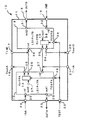
図1は、本発明の半導体装置の一実施の形態を示す概念図である。
図1に示すように、本半導体装置10は、複数(図では二つであるが限定されない。)のLSIチップA12、LSIチップB13を一つのパッケージ11に内蔵し、各LSIチップA12、LSIチップB13間の接続をパッケージ11の内部で行った半導体装置である。本半導体装置10は、それぞれのLSIチップA12、LSIチップB13が個別にされるテストと同様のテストがパッケージ化された状態であっても、同時に実施することができる様にする為に、それぞれのLSIチップA、B内にセレクタ回路(以下「セレクタ」という。)を内蔵している事、通常使用時からテスト状態に切り替える為のテスト切り替え端子を1本設けている事、LSIチップA12、LSIチップB13のテスト時だけに使用するテスト用端子をパッケージの通常使用しない端子箇所に設けている事を特徴とする。
FIG. 1 is a conceptual diagram showing an embodiment of a semiconductor device of the present invention.
As shown in FIG. 1, the
図1に示すように、セレクタA14を内蔵するLSIチップA12と、セレクタB15を内蔵するLSIチップB13とが一つのパッケージ11に内蔵されている。LSIチップA12は、二つの端子in1(30)、in2(27)、制御端子である端子TESTA28、出力端子である端子out1(29)、out2(37)、およびセレクタA14の出力端子に接続された二つの端子25、26を有する。LSIチップB13は、二つの端子in1(36)、in2(32)、端子TESTB33、端子out1(38)、out2(31)、およびセレクタB15の出力端子に接続された二つの端子34、35を有する。
As shown in FIG. 1, an LSI chip A12 containing a selector A14 and an LSI chip B13 containing a selector B15 are built in one
パッケージ11は、通常の動作を行うための端子(図示せず)の他に複数(図では9本であるが限定されない。)のテスト用端子を有する。テスト用端子としては、セレクタA14、セレクタB15に制御用の信号を入力するための端子TEST22、テスト信号の入力端子である端子INA24、INB19、TinA21、TinB17、出力端子である端子OUTA23、OUTB18、ToutA16、ToutB20を有する。
セレクタA14は、LSIチップA12の端子out2(37)に接続された一つの信号入力端子と、LSIチップA12の端子TESTAに接続された一つの制御信号入力端子と、LSIチップA12の出力端子25、26に接続された二つのデータ出力端子とを有する。セレクタA14は、例えば、入力端子を共通接続した二つのトライステート(登録商標)バッファからなっている。
セレクタA14は、制御信号入力端子に制御信号が入力されていないときは端子ToutA側の出力端子がハイインピーダンス状態(例えば、出力端子をオープンにした状態)になり、制御信号入力端子に制御信号が入力されているときは接続先のLSIチップB13側の出力端子がハイインピーダンス状態になる。
The
The selector A14 has one signal input terminal connected to the terminal out2 (37) of the LSI chip A12, one control signal input terminal connected to the terminal TESTA of the LSI chip A12, an
In the selector A14, when the control signal is not input to the control signal input terminal, the output terminal on the terminal ToutA side is in a high impedance state (for example, the output terminal is opened), and the control signal is input to the control signal input terminal. When the signal is input, the output terminal on the connection side LSI chip B13 side is in a high impedance state.
セレクタB15は、セレクタA14と同様に、入力端子を共通接続した二つのトライステート(登録商標)バッファからなり、制御信号入力端子に制御信号が入力されていないときは出力端子ToutB側の出力端子がハイインピーダンス状態になり、制御信号入力端子に制御信号が入力されているときは接続先のLSIチップA12側の出力端子がハイインピーダンス状態になる。 Similarly to the selector A14, the selector B15 includes two tristate (registered trademark) buffers having input terminals connected in common. When no control signal is input to the control signal input terminal, the output terminal on the output terminal ToutB side is When the control signal is input to the control signal input terminal, the output terminal on the connection side LSI chip A12 side is in the high impedance state.
すなわち、本発明の半導体装置10は、図1に示すように、LSIチップA12、LSIチップB13にテスト専用の端子(TESTA28、TESTB33)をそれぞれ1本ずつ設け、それらのテスト専用の端子28、33を制御(セレクタA14、セレクタB15をON/OFFさせるための電圧のON/OFF)することで、LSIチップA12の指定された端子にテストする信号を入力し、さらに他のLSIチップB13に接続される出力端子をハイインピーダンス状態に設定する事を可能としており、LSIチップA12、LSIチップB13のテスト時にのみ使用するテスト用の端子をパッケージ11で通常使用しない端子箇所に設けていることを特徴とする。
That is, in the
本発明の第1の実施の形態について図1を用いてさらに説明する。
図1に示す装置は、LSIチップA12およびLSIチップB13の2つのLSIチップが、1つのパッケージ11に内蔵された半導体装置であり、それぞれのLSIチップA12およびLSIチップB13に設けられたテスト専用の端子(TESTA28、TESTB33)を制御することで、LSIチップA12とLSIチップB13とを並列にテスト出来るよう、セレクタA14、セレクタB15と、LSIチップA12、LSIチップB13のテスト時にのみ使用する端子(TinA21、ToutA16、TinB17、ToutB20)を設けている。
The first embodiment of the present invention will be further described with reference to FIG .
The device shown in FIG. 1 is a semiconductor device in which two LSI chips, LSI chip A12 and LSI chip B13, are built in one
ここで、「並列にテスト出きる」とは、二つのセレクタA14およびセレクタB15を同時に動作させ、二つのLSIチップA12、LSIチップB13を同時にそれぞれのテスト用の端子TinA21、ToutA16、TinB17、ToutB20に接続し、それぞれのテスト用の端子TinA21、TinB17にテスト信号(例えば、「1」論理レベルの信号、すなわちH)を入力し、それぞれの出力端子である端子ToutA16、ToutB20、OUTA23、OUTB18で電圧や波形等を測定することをいう。 Here, “test can be performed in parallel” means that the two selectors A14 and B15 are operated simultaneously, and the two LSI chips A12 and B13 are simultaneously connected to the test terminals TinA21, ToutA16, TinB17, and ToutB20. The test signals (for example, signals of “1” logic level, that is, H) are input to the test terminals TinA21 and TinB17, respectively, and the voltage at the output terminals ToutA16, ToutB20, OUTA23, and OUTB18 This refers to measuring a waveform or the like.
図2は、図1に示した半導体装置のパッケージの底面図である。
図2において、LSIチップA12とLSIチップB13とが内蔵されたパッケージ11の例として、BGA(Ball Grid Array )の端子配置を表した底面が示されており、パッケージ11の中心部分41の端子42が、LSIチップA12、LSIチップB13のテスト時にのみ使用する端子(TinA21、ToutA16、TinB17、ToutB20)として用いられている。この事は、通常時に使用される端子40はパッケージ11の外周に設けられている為、本発明の半導体装置10を、他の部品や他のLSIパッケージとプリント基板等に搭載して接続する場合などは、接続がし易くなり、検査効率が向上するので有利である。
尚、図2に示す半導体装置は端子数(ボール数)が計200個の場合を示しているが、本発明はこれに限定されるものではなく、ボール数が200個以上であっても200個未満であってもよい。また、本実施の形態では端子40がパッケージ11の外周部に設けられ、テスト用の端子42がパッケージ11の中央部に設けられた場合を示しているが、本発明はこれに限定されるものではなく、フルグリッドアレイタイプであってもよい。さらに、本実施の形態ではBGA型の半導体装置の場合で説明したが、本発明はこれに限定されるものではなく、PGA(Pin Grid Array)型の半導体装置であってもよい。
FIG. 2 is a bottom view of the package of the semiconductor device shown in FIG.
In FIG. 2, as an example of the
2 shows a case where the total number of terminals (the number of balls) is 200, the present invention is not limited to this, and even if the number of balls is 200 or more, the semiconductor device is 200. It may be less than one. In this embodiment, the terminal 40 is provided on the outer peripheral portion of the
LSIチップA12とLSIチップB13とをテストする場合、端子TEST22の論理レベルが半導体装置10を製品として機能動作する時と反対となるよう指定する事で、セレクタA14は、端子out2(37)からの信号を端子ToutA16に出力し、LSIチップB13の端子in1(36)に接続されるセレクタA14の出力端子は、ハイインピーダンスを出力する。
同様に、セレクタB15は、端子out1(29)からの信号を端子ToutB20に出力し、LSIチップA12の端子in2(27)に接続されるセレクタB15の出力端子は、ハイインピーダンスを出力する。
When testing the LSI chip A12 and the LSI chip B13, the selector A14 is connected to the terminal out2 (37) by designating that the logic level of the terminal TEST22 is opposite to that when the
Similarly, the selector B15 outputs a signal from the terminal out1 (29) to the terminal ToutB20, and the output terminal of the selector B15 connected to the terminal in2 (27) of the LSI chip A12 outputs a high impedance.
以上のような接続を実現することで、LSIチップA12をテストする時は、端子INA24および端子TinA21によりテスト信号を入力し、端子OUTA23および端子ToutA16にてテスト結果を判定することができる。LSIチップB13をテストする時は、INB19およびTinB17よりテスト信号を入力し、端子OUTB18および端子ToutB20にてテスト結果を判定する。 By realizing the connection as described above, when testing the LSI chip A12, a test signal can be input through the terminal INA24 and the terminal TinA21, and the test result can be determined at the terminal OUTA23 and the terminal ToutA16. When testing LSI chip B13, a test signal is input from INB19 and TinB17, and the test result is determined at terminal OUTB18 and terminal ToutB20.
また、テスト時以外の各LSIチップA12、LSIチップB13が製品として機能動作する通常動作においては、端子TESTの論理をテスト時とは反対になるように指定し、LSIチップA12の端子out2(37)からの信号をセレクタA14の切り替えによりLSIチップB13の端子in1(36)に接続するようにし、端子ToutA16に接続されるセレクタA14の出力をハイインピーダンス状態にする。
同様に、LSIチップB13の端子out1(38)からの信号をセレクタB15の切り替えによりLSIチップA12のin2(27)に接続するようにし、端子ToutB20に接続されるセレクタB15の出力は、ハイインピーダンス状態にする。
このように、テスト時に使用する端子は、通常動作時はハイインピーダンス状態となるので、端子処理としてもオープン扱いが可能となる。
Further, in the normal operation in which each LSI chip A12 and LSI chip B13 function as products other than during the test, the logic of the terminal TEST is specified to be opposite to that during the test, and the terminal out2 (37 of the LSI chip A12) ) Is connected to the terminal in1 (36) of the LSI chip B13 by switching the selector A14, and the output of the selector A14 connected to the terminal ToutA16 is set to a high impedance state.
Similarly, the signal from the terminal out1 (38) of the LSI chip B13 is connected to in2 (27) of the LSI chip A12 by switching the selector B15, and the output of the selector B15 connected to the terminal ToutB20 is in a high impedance state. To.
In this way, since the terminals used during the test are in a high impedance state during normal operation, the terminals can be handled as open.
(効果の説明)
複数のLSIチップを一つのパッケージに内蔵した半導体装置の状態においても、それぞれのLSIチップが1個づつ個別部品としてテストされる時と同じテストを同時に行う事を可能とし、十分なテストを行える状況にすることで、検査コストの上昇を防ぐ効果と、最終製品への不良品の混入を低減できる効果とが得られる。
(Explanation of effect)
Even in the state of a semiconductor device in which multiple LSI chips are built in one package, it is possible to perform the same test as when each LSI chip is tested as an individual component one by one, and a sufficient test can be performed By doing so, it is possible to obtain the effect of preventing an increase in the inspection cost and the effect of reducing the mixing of defective products into the final product.
(第2の実施の形態)
第2の実施の形態について図3を用いて説明する。
図3は、本発明の半導体装置の他の実施の形態を示す概念図である。尚、図1に示した実施の形態と同様の部材には共通の符号を用いた。
第2の実施の形態は、第1の実施の形態においてのLSIチップA12に内蔵されていたセレクタA14をLSIチップA12の外部に出し、テスト専用の端子TESTA28(図1参照)を削除し、同様にLSIチップB13に内蔵されていたセレクタB15をLSIチップB13の外部に出し、テスト専用の端子TESTB3(図1参照)を削除し、LSIチップA51、LSIチップB52、セレクタA53およびセレクタB54をパッケージ11に内蔵したものである。図3に示す半導体装置50は、LSIチップA51およびLSIチップB52をテストする場合の動作及びテスト以外の通常の動作については、第1の実施の形態と同様である。
(Second Embodiment)
A second embodiment will be described with reference to FIG.
FIG. 3 is a conceptual diagram showing another embodiment of the semiconductor device of the present invention. In addition, the same code | symbol was used for the member similar to embodiment shown in FIG.
In the second embodiment, the selector A14 incorporated in the LSI chip A12 in the first embodiment is brought out of the LSI chip A12, the test dedicated terminal TESTA28 (see FIG. 1) is deleted, and the like. The selector B15 built in the LSI chip B13 is taken out of the LSI chip B13, the test-dedicated terminal TESTB3 (see FIG. 1) is deleted, and the LSI chip A51, LSI chip B52, selector A53, and selector B54 are packaged. It is built in. The semiconductor device 50 shown in FIG. 3 is the same as that of the first embodiment in the operation when testing the LSI chip A51 and the LSI chip B52 and the normal operation other than the test.
(第3の実施の形態)
図4は、本発明の半導体装置の他の実施の形態を示す概念図である。
第3の実施の形態としての半導体装置70は、セレクタA53およびセレクタB54の機能を、LSIチップA51およびLSIチップB52とは別のLSIチップとして実現する事も可能である。
(Third embodiment)
FIG. 4 is a conceptual diagram showing another embodiment of the semiconductor device of the present invention.
The
(第4の実施の形態)
図5は、本発明の半導体装置の他の実施の形態を示す概念図である。
第4の実施の形態としての半導体装置80は、端子TinA21とLSIチップA51の端子in2(56)の間に新たに別のセレクタ82を設け、端子TEST22の制御にて通常動作時は、端子TinA21からの信号を電気的に切断し、端子TinA21にぶら下がる配線容量(分布容量)を少なくする事で、LSIチップB52の端子out1(61)とLSIチップA51の端子in2(56)との間の伝送信号を高速に送る事が可能となる。同様にTinB端子17とLSIチップB52の端子in1(62)との間に新たに別のセレクタ81を設け端子TEST22の制御にて通常動作時は、端子TinB17にぶら下がる配線容量(分布容量)を少なくし、LSIチップA51の端子out2(55)とLSIチップB52の端子in1(62)との間の伝送信号を高速に送る事が可能となる。
尚、本実施の形態では、セレクタ81、82がLSIチップA51、LSIチップB52の外部に設けられた場合で説明したが、本発明はこれに限定されるものではなく、第1の実施の形態のように各LSIチップA51、LSIチップB52にそれぞれ内蔵されていてもよく、第3の実施の形態のようにLSIチップ70の中に内蔵されていてもよい。
(Fourth embodiment)
FIG. 5 is a conceptual diagram showing another embodiment of the semiconductor device of the present invention.
In the
In the present embodiment, the
10 半導体装置
11 パッケージ
12 LSIチップA
13 LSIチップB
14 セレクタA(セレクタ回路A)
15 セレクタB(セレクタ回路B)
16 ToutA(端子)
17 TinB(端子)
18 OUTB(端子)
19 INB(端子)
20 ToutB(端子)
21 TinA(端子)
22 TEST(端子)
23 OUTA(端子)
24 INA(端子)
10
13 LSI chip B
14 Selector A (Selector circuit A)
15 Selector B (Selector circuit B)
16 ToutA (terminal)
17 TinB (terminal)
18 OUTB (terminal)
19 INB (terminal)
20 ToutB (terminal)
21 TinA (terminal)
22 TEST (terminal)
23 OUTA (terminal)
24 INA (terminal)
Claims (4)
前記各LSIチップの間に配置され、テスト時に前記パッケージの外部からの信号により前記各LSIチップの出力信号を接続先の他のLSIチップから前記パッケージの外部に出力自在に切り替えるセレクタ回路と、
前記パッケージの通常動作時用の端子とは異なる位置に配置され、テスト時に前記パッケージの外部と信号の授受が行われる複数のテスト用の端子と、
前記テスト用の端子のうち外部からの信号が入力される端子と前記各LSIチップの入力用の端子との間に配置され、通常動作時には前記テスト用の端子と前記各LSIチップの入力用の端子との間を切断する他のセレクタ回路を有し、前記テスト用の端子から前記各LSIチップとの間の分布容量を減少させることにより、前記各LSIチップ間の伝送信号を高速に送るようにしたことを特徴とする半導体装置。 In a semiconductor device in which a plurality of LSI chips are electrically connected to each other and incorporated in one package,
A selector circuit disposed between the LSI chips and configured to switch an output signal of each LSI chip from a connected other LSI chip to the outside of the package by a signal from the outside of the package at the time of testing;
A plurality of test terminals which are arranged at positions different from the terminals for normal operation of the package, and which are used to exchange signals with the outside of the package at the time of testing;
The test terminal is disposed between a terminal to which an external signal is input and an input terminal of each LSI chip, and is used for input of the test terminal and each LSI chip during normal operation. Another selector circuit that cuts the connection between the terminals is provided, and the transmission capacity between the LSI chips is transmitted at high speed by reducing the distributed capacitance between the test terminals and the LSI chips. A semiconductor device characterized by that.
Priority Applications (1)
| Application Number | Priority Date | Filing Date | Title |
|---|---|---|---|
| JP2003390168A JP4457648B2 (en) | 2003-11-20 | 2003-11-20 | Semiconductor device |
Applications Claiming Priority (1)
| Application Number | Priority Date | Filing Date | Title |
|---|---|---|---|
| JP2003390168A JP4457648B2 (en) | 2003-11-20 | 2003-11-20 | Semiconductor device |
Publications (2)
| Publication Number | Publication Date |
|---|---|
| JP2005148026A JP2005148026A (en) | 2005-06-09 |
| JP4457648B2 true JP4457648B2 (en) | 2010-04-28 |
Family
ID=34696640
Family Applications (1)
| Application Number | Title | Priority Date | Filing Date |
|---|---|---|---|
| JP2003390168A Expired - Fee Related JP4457648B2 (en) | 2003-11-20 | 2003-11-20 | Semiconductor device |
Country Status (1)
| Country | Link |
|---|---|
| JP (1) | JP4457648B2 (en) |
Families Citing this family (1)
| Publication number | Priority date | Publication date | Assignee | Title |
|---|---|---|---|---|
| JP5029073B2 (en) * | 2007-03-07 | 2012-09-19 | 株式会社デンソー | Semiconductor device and method for testing semiconductor device |
-
2003
- 2003-11-20 JP JP2003390168A patent/JP4457648B2/en not_active Expired - Fee Related
Also Published As
| Publication number | Publication date |
|---|---|
| JP2005148026A (en) | 2005-06-09 |
Similar Documents
| Publication | Publication Date | Title |
|---|---|---|
| US4504783A (en) | Test fixture for providing electrical access to each I/O pin of a VLSI chip having a large number of I/O pins | |
| US7466158B2 (en) | Multilayer semiconductor device | |
| US20010039646A1 (en) | Structure having multiple levels of programmable integrated circuits for interconnecting electronic components | |
| JP5024740B2 (en) | LSI chip testing equipment | |
| WO1988002553A2 (en) | Integrated circuit packaging configuration for rapid customized design and unique test capability | |
| US7579689B2 (en) | Integrated circuit package, and a method for producing an integrated circuit package having two dies with input and output terminals of integrated circuits of the dies directly addressable for testing of the package | |
| US20080141089A1 (en) | Semiconductor Integrated Circuit and System Lsi | |
| US6356095B1 (en) | Semiconductor integrated circuit | |
| EP1358498B1 (en) | Input/output continuity test mode circuit | |
| JP4457648B2 (en) | Semiconductor device | |
| JPH04250644A (en) | Multichip mounting ic | |
| US20080197872A1 (en) | Semiconductor chip, multi-chip semiconductor device, inspection method of the same, and electric appliance integrating the same | |
| KR20080061735A (en) | Device under test and system and method for testing the same | |
| JP2004037254A (en) | Scanning test device | |
| JP4525125B2 (en) | Multi-chip type semiconductor device | |
| JP2007114163A (en) | Multi-chip package lsi | |
| JP2009085934A (en) | Testing device having switching element on socket substrate | |
| JPH04128666A (en) | Semiconductor integrated circuit | |
| EP0502210B1 (en) | Semiconductor integrated circuit device with testing-controlling circuit provided in input/output region | |
| JP2558819B2 (en) | Multi-pin LSI with test circuit for soldering defect inspection | |
| JP2001305187A (en) | Circuit board and inspection device for the circuit board | |
| JP2008164623A (en) | Semiconductor device | |
| JPH02105452A (en) | Output circuit of semiconductor integrated circuit | |
| JP2000009800A (en) | Scan test circuit and semiconductor device equipped with the same and scan testing method therefor | |
| JP4234826B2 (en) | Method for evaluating semiconductor integrated circuit |
Legal Events
| Date | Code | Title | Description |
|---|---|---|---|
| A621 | Written request for application examination |
Free format text: JAPANESE INTERMEDIATE CODE: A621 Effective date: 20061013 |
|
| A977 | Report on retrieval |
Free format text: JAPANESE INTERMEDIATE CODE: A971007 Effective date: 20090511 |
|
| A131 | Notification of reasons for refusal |
Free format text: JAPANESE INTERMEDIATE CODE: A131 Effective date: 20090519 |
|
| A521 | Request for written amendment filed |
Free format text: JAPANESE INTERMEDIATE CODE: A523 Effective date: 20090717 |
|
| A131 | Notification of reasons for refusal |
Free format text: JAPANESE INTERMEDIATE CODE: A131 Effective date: 20090804 |
|
| A521 | Request for written amendment filed |
Free format text: JAPANESE INTERMEDIATE CODE: A523 Effective date: 20091002 |
|
| A131 | Notification of reasons for refusal |
Free format text: JAPANESE INTERMEDIATE CODE: A131 Effective date: 20091027 |
|
| A521 | Request for written amendment filed |
Free format text: JAPANESE INTERMEDIATE CODE: A523 Effective date: 20091222 |
|
| TRDD | Decision of grant or rejection written | ||
| A01 | Written decision to grant a patent or to grant a registration (utility model) |
Free format text: JAPANESE INTERMEDIATE CODE: A01 Effective date: 20100119 |
|
| A01 | Written decision to grant a patent or to grant a registration (utility model) |
Free format text: JAPANESE INTERMEDIATE CODE: A01 |
|
| A61 | First payment of annual fees (during grant procedure) |
Free format text: JAPANESE INTERMEDIATE CODE: A61 Effective date: 20100201 |
|
| R150 | Certificate of patent or registration of utility model |
Free format text: JAPANESE INTERMEDIATE CODE: R150 |
|
| FPAY | Renewal fee payment (event date is renewal date of database) |
Free format text: PAYMENT UNTIL: 20130219 Year of fee payment: 3 |
|
| FPAY | Renewal fee payment (event date is renewal date of database) |
Free format text: PAYMENT UNTIL: 20130219 Year of fee payment: 3 |
|
| FPAY | Renewal fee payment (event date is renewal date of database) |
Free format text: PAYMENT UNTIL: 20140219 Year of fee payment: 4 |
|
| S111 | Request for change of ownership or part of ownership |
Free format text: JAPANESE INTERMEDIATE CODE: R313113 |
|
| R350 | Written notification of registration of transfer |
Free format text: JAPANESE INTERMEDIATE CODE: R350 |
|
| R250 | Receipt of annual fees |
Free format text: JAPANESE INTERMEDIATE CODE: R250 |
|
| R250 | Receipt of annual fees |
Free format text: JAPANESE INTERMEDIATE CODE: R250 |
|
| LAPS | Cancellation because of no payment of annual fees |