JP4457551B2 - Integrated circuit protection against electrostatic discharge and overvoltage - Google Patents
Integrated circuit protection against electrostatic discharge and overvoltage Download PDFInfo
- Publication number
- JP4457551B2 JP4457551B2 JP2002307000A JP2002307000A JP4457551B2 JP 4457551 B2 JP4457551 B2 JP 4457551B2 JP 2002307000 A JP2002307000 A JP 2002307000A JP 2002307000 A JP2002307000 A JP 2002307000A JP 4457551 B2 JP4457551 B2 JP 4457551B2
- Authority
- JP
- Japan
- Prior art keywords
- circuit
- integrated circuit
- mosswi
- conductor
- transistor
- Prior art date
- Legal status (The legal status is an assumption and is not a legal conclusion. Google has not performed a legal analysis and makes no representation as to the accuracy of the status listed.)
- Expired - Lifetime
Links
Images


Classifications
-
- H—ELECTRICITY
- H10—SEMICONDUCTOR DEVICES; ELECTRIC SOLID-STATE DEVICES NOT OTHERWISE PROVIDED FOR
- H10D—INORGANIC ELECTRIC SEMICONDUCTOR DEVICES
- H10D89/00—Aspects of integrated devices not covered by groups H10D84/00 - H10D88/00
- H10D89/60—Integrated devices comprising arrangements for electrical or thermal protection, e.g. protection circuits against electrostatic discharge [ESD]
- H10D89/601—Integrated devices comprising arrangements for electrical or thermal protection, e.g. protection circuits against electrostatic discharge [ESD] for devices having insulated gate electrodes, e.g. for IGFETs or IGBTs
- H10D89/811—Integrated devices comprising arrangements for electrical or thermal protection, e.g. protection circuits against electrostatic discharge [ESD] for devices having insulated gate electrodes, e.g. for IGFETs or IGBTs using FETs as protective elements
Landscapes
- Semiconductor Integrated Circuits (AREA)
- Metal-Oxide And Bipolar Metal-Oxide Semiconductor Integrated Circuits (AREA)
Description
【0001】
【発明の属する技術分野】
本発明は静電放電及び他の過電圧からの集積回路の保護に関する。本発明は特に保護に必要な回路の集積に関する。
【0002】
【従来の技術】
静電放電(ESD)に対する保護回路は電子回路をその端子から来る静電放電に対して保護することを意図している。
【0003】
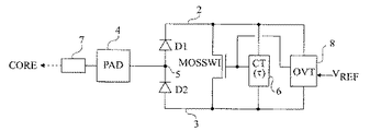
図1は従来の電子保護回路1の例を示す。この回路の機能は、回路のパッド4に印加される静電放電による過電圧が発生したときに、集積回路の供給ライン2と3を短絡することである。この一連の接続の中間点5は電気的にパッド4に接続される。ダイオードD1とD2は、通常動作で、オフになるようにバイアスされる。従って、図1の例で、線2は正の供給線、線3は負の供給線(一般に接地)を形成する。回路1は又供給線2と3の間にMOSトランジスタMOSSWIをふくみ、そのゲートは少なくともひとつのESD保護制御回路6に接続される。
【0004】
パッド4が受信する静電タイプの妨害は正又は負の電荷により形成される。この種の電荷があらわれるとダイオードD1とD2の一方が導通する。次にトランジスタMOSSWIがオンとなって供給線2と3を短絡し、従って過剰電荷を導通放散させる。電荷をトランジスタMOSSWIに流すことによりコアへの損害が避けられる。ダイオードD1又はD2による電気回路の抵抗が回路のコアを通る抵抗より小さくなることを保証するために、パッド4と集積回路コアの間に抵抗7がもうけられる。
【0005】
従って、回路6(CT)は、静電放電が発生したとき、つまり、電流がダイオードD1又はD2に流れたときに、トランジスタMOSSWIをトリガする時定数(τ)を設定する。回路6は一般に抵抗性及び容量性の回路(RCセル)で形成される。
【0006】
供給導体を短絡するトランジスタMOSSWIは、又、集積回路技術で許される最大値に関し過電圧に対する保護としても使用される。この場合、別の制御回路8(OVT)が過電圧(例えば所定の電圧スレシュホールドVrefに関して)を検出し、回路に関連するトランジスタMOSSWIをオンにする機能を有する。従って集積回路は静電放電ばかりでなく、発生源が何であれ過電圧に対しても保護される。
【0007】
以後の説明では静電放電(ESD)に対する保護に対する電子保護回路を例示する。そして、特に明示しない限り過電圧に対する保護もふくむ。
【0008】
電子保護回路1の特徴の中で特に注目すべきは、トランジスタMOSSWIのオン状態抵抗(RdsON)を出来るだけ小さくして、その保護作用を達成させ過電圧が回路の他の個所に伝播するのを防止するようにするということである。その結果、トランジスタMOSSWI(一般にNチャネルMOSトランジスタ)は、過剰な電荷を急速に導通させるために大きなサイズを有する。
【0009】
過電圧を検出するための制御回路6は一般に低い時定数(多くの場合200ns以下)をもたなければならない。
【0010】
その結果、一般に、保護回路のトランジスタMOSSWIを保護対象のパッド4に出来るだけ近く配置することが望ましい。これは、実際の供給線と、パッドとトランジスタ端子の間の区間によりもたらされる抵抗を小さくするためである。
【0011】
さらに、従来、制御回路自身をトランジスタMOSSWIに出来るだけ近く配置して、制御回路6の容量素子を形成する制御回路とトランジスタMOSSWIのゲートの間の導電路による抵抗を小さくしている。
【0012】
図2は従来の集積回路10の上面図で、ESD保護回路に関連するパッド4を有する。図2の例では、3個のパッド4(PAD)と2個のESD保護回路1が示されている。上述の近接の理由により、保護回路1は集積回路のいわゆるクラウンの位置に置かれる。このクラウンは集積回路の特定の応用に関連する異なる機能を集積する回路コアを囲んでいる。
【0013】
回路10のクラウンは一般に集積回路の正の電源電圧VPと負の電源電圧VNを運ぶ少なくとも2つの導体12,13をふくむ給電レール11(BUS)をふくむ。必要ならば、給電レール11は他の導体、例えば、集積回路が正の供給電圧をもつならば接地と負の供給電圧をふくむことができる。
【0014】
給電バスは集積回路の周辺部に部分的に、又は異なって(例えば中央部)に配置することができる。コアの表記は、その位置にかかわらず、集積回路に特有の応用に関連し、任意の形態のバスで給電される集積素子をとり囲む。
【0015】
回路1の各トランジスタMOSSWIは、各々、導体14,15により給電バスの導体12,13に接続される。同様に、各パッド4はダイオード(図1のD1,D2,図2には図示なし)を介して導体12,13に接続される。
【0016】
接続パッドの観点から、2つの大規模集積回路ファミリーが区別される。
【0017】
第1のファミリーはパッド制限回路と呼ばれる。ここでは、集積回路コアから外部への多数の接続バッドが、パッドの配列に必要な周囲長のため実際の集積回路のサイズを条件づける。
【0018】
第2のファミリーはコア制限回路と呼ばれ、そのサイズは、パッドの配列のための周囲長ではなく、コアの表面積により限定される。
【0019】
第1のファミリーの回路では、集積回路を静電放電から正しく保護するための十分な数のMOSSWIトランジスタとその制御回路を形成するために必要な空間は集積回路コアの中で確保することができる。
【0020】
しかし、集積回路コアにより既にサイズが決定されている回路では、ESD保護回路のMOSSWIトランジスタを形成するためにコアのサイズを増加させることは、回路にとって有害である。代表的には、保護回路はチップコアサイズの10%までを占め、所望の小型化に悪い影響を与える。
【0021】
【発明が解決しようとする課題】
本発明はサイズの小さな電子保護素子をもった集積回路を提供することを目的とする。
【0022】
本発明は特に電子保護素子をもったコア制限型の集積回路の体積を減少させることを目的とする。
【0023】
本発明は更にESD保護の品質に悪影響がないか又はむしろそれを改良する解決を提供することを目的とする。
【0024】
本発明は更に任意の型の過電圧から集積回路を保護する解決を提供することを目的とする。
【0025】
本発明は更に現在の集積回路の製造技術と互換性のある解決を提供することを目的とする。
【0026】
【課題を解決するための手段】
上記目的及び他の目的を達成するために、本発明は、
レールに形成される供給導体を短絡する少なくともひとつのスイッチを有し電子保護の少なくともひとつの素子を有する集積回路において、
前記スイッチが前記導体の下で前記レールに集積化され、
前記スイッチ(MOSSWI)はMOSトランジスタで構成され、それらのドレインとソースは各々前記集積回路の2つの供給導体(12,13)の一方に接続され、
前記レール(11)に、前記MOSトランジスタのゲートの制御のための別の導体(23)がもうけられ、
前記MOSトランジスタのゲートは、前記レールの前記供給導体(12,13)に対して垂直にもうけられ、該ゲートは、ゲートの制御のための前記別の導体(23)にビア(27)により接続される集積回路を提供する。
【0027】
本発明の実施例によると、少なくともひとつの第1の共通回路により数個のスイッチが制御される。
【0028】
本発明の実施例によると、前記第1の共通回路は静電電荷の発生を検出する。
【0029】
本発明の実施例によると、前記供給導体の間の過電圧の発生を検出する少なくともひとつの第2制御回路をふくむ。
【0030】
本発明の実施例によると、短絡スイッチのための前記制御回路は、前記集積回路のコアにもうけられる。
【0034】
【発明の実施の形態】
異なる図で、同じ部材は同じ参照番号で示す。明瞭化のために本発明の理解に必要な素子のみを図示し記述する。特に、集積回路の応用機能は詳述しない。本発明は集積回路の応用にかかわらず適用可能である。
【0035】
本発明の特徴は、静電放電又は過電圧に対する電子保護素子のMOSSWIトランジスタを集積化する集積回路の供給レールの下のシリコン表面を利用することにある。
【0036】
空間を倹約するためには、集積回路の応用に特有の素子を供給レールの下に集積化することが考えられる。しかし、応用のコア回路の接続が相互接続のためのメタライゼーション層を必要とするので、上述の解決は不十分である。現在、供給レールでは、全てのメタライゼーション層は実際の供給導体(図2の12,13)を形成するために使用され、供給レールの幅を減少させてその厚さを増加させ、従って回路が大形になっていた。
【0037】
本発明は、電子保護素子(特にESD)のスイッチ(MOSSWI)とその接続が正と負の供給信号と制御信号のみしか必要としないという事実を利用する。供給導体は既にレールの中に存在するので、本発明はシリコン表面の上へのMOSSWIトランジスタの集積を提供する。
【0038】
図3は本発明による集積回路20の実施例の上面図を図2との比較で示す。
【0039】
集積回路20のコアの外部への接続のためのパッドと、正の給電電圧VPを運ぶ導体12と負の給電電圧VN(一般には接地)を運ぶ導体13をふくむ給電レール(例えば、周辺)がふくまれる。
【0040】
本発明によると、電子保護回路(ESD及び/又は過電圧)のMOSSWIトランジスタは給電レールの導体12と13の下に配置される。MOSSWIトランジスタの導体12,13への接続は図3では21,22により示され、これらは図2の14,15と比較される。本発明の回路のMOSSWIトランジスタの制御は、RCセル型の遅延回路で構成される前述と同様の制御回路6により提供される制御信号CTRLを運ぶ導体23によって提供される。回路6は従来通り給電導体に接続される(図2及び図3には図示なし)。
【0041】
本発明の特徴として単一のESD保護制御回路6で、集積回路全体に対して十分である。従来の技術で制御回路は多くの空間を占める素子ではないが、本発明は回路の体積の減少に有効である。しかし、例えば、制御信号のアクセス抵抗を減少したいときは、数個の制御回路をもうけることもできる。そのとき、全ての制御回路は制御導体23に並列に接続される。
【0042】
同様に、集積回路全体に対して、過電圧に対する保護に対しては、単一の制御回路8で十分である。
【0043】
本発明の実施のためには制御信号CTRLを運ぶ導体をレールに追加しなければならない。しかし、この導体は大きな断面を必要としない。従って、それが占める空間は小さい。さらに、レールにおいて全てのメタライゼーション層の利用が可能であるので、この制御信号を構成するためにひとつのメタライゼーション層のわずかな区間を割り当てることは問題がない。従来、レールにあらわれる2つの信号は、本発明の実施のために、大きな断面(供給導体)を必要とする。
【0044】
図4は本発明の第1実施例によるMOSSWIトランジスタの構成の断面の斜視図である。図示のごとく、トランジスタは供給レールの導体12,13と垂直に形成される。これにより、各トランジスタのドレインとソース(図示なし)の、導体12,13からの接点(及びビア)25,26による接続が容易になる。従って、図4の実施例で、小さな多数のMOSトランジスタが供給レール11の下に分布する。小さいということは、多数を並列接続することにより補償され、小さな直列抵抗で所望のトランジスタ表面積が得られる。
【0045】
本発明のここにあらわれる別の利点は集積回路の各パッド4が必然的に近接したトランジスタ群をもつことである。
【0046】
図4の実施例で、トランジスタのゲートGの接続は、図3の実施例に反して、導体12と13の横、つまり供給レールの内側又は外側の周囲にもうけられる信号CTRLを運ぶ導体23により行われる。導体23のゲートGへの接続は1又は複数の接点、及びおそらくはビア27により行われる。図4でゲートGの両側には厚い酸化領域29のみを示す。トランジスタは従来の技術によりシリコンの中に実現することができる。
【0047】
図5は本発明の第2実施例の上面を部分的に示す。この実施例はMOSSWIトランジスタの制御導体23が供給レール11の中央にある場合を示す。図5の実施例で、レール11のみが図示され、レール11は正の供給導体12が2つの接地導体13に囲まれた構造を有する。
【0048】
図4の実施例のように、MOSSWIトランジスタのゲートGは供給レール11の導体に垂直である。図5の実施例でゲートGを導体23に接続するための複数のビア27が示され、一方、各トランジスタのドレインとソースを供給導体に接続するための単一のビア、各々25と26、が示される。しかし、ビアの数は電流と応用に従って場合毎に適応される。図5の実施例では集積回路基板を接地にバイアスするための別のシリーズのビア28が図示される。
【0049】
本発明の利点は電子保護素子(特にESD)が占有する表面が応用のためのコア表面積に比べて非常に小さいことにある。
【0050】
本発明の別の利点は保護素子のMOSSWIトランジスタの分布が、表面積を最少にするために保護素子の数を少なくしていた従来の技術の場合よりも、一様なことである。
【0051】
もちろん、本発明の変形、修飾、改良は当業者に容易である。特に、電子保護素子(ESD又は過電圧)、特にMOSSWIトランジスタの実際の実現は応用と上記の機能的記述にもとづいて当業者に容易である。本発明のMOSSWIトランジスタのゲート容量はトランジスタの表面積との比較で従来のMOSSWIトランジスタよりも大きい。さらに、保護回路のダイオードD1,D2の形成については詳述しないが、ダイオードは従来と同様にレールの外側でパッド4に出来るだけ近接して置くことができる。
【0052】
上述の変更、修飾、改良は本記載の一部であり、本発明の精神の範囲に含まれる。従って、上述の記述は単なる例であり、発明を限定しない。本発明は請求の範囲とその均等によってのみ限定される。
【図面の簡単な説明】
【図1】静電放電と過電圧に対する従来の保護回路を示す。
【図2】集積回路の過電圧に対する従来の回路の例である。
【図3】本発明による電子保護回路を示す。
【図4】本発明による集積回路の供給レールに関するMOSSWIトランジスタの第1の実施例の斜視図である。
【図5】本発明による集積回路の供給レールに関するMOSSWIトランジスタの第2実施例を示す。
【符号の説明】
4 パッド
6 制御回路
11 給電レール
12,13 導体
20 集積回路
21,22 導体
23 導体
MOSSWI MOSトランジスタ
CORE コア[0001]
BACKGROUND OF THE INVENTION
The present invention relates to the protection of integrated circuits from electrostatic discharge and other overvoltages. The invention particularly relates to the integration of the circuits necessary for protection.
[0002]
[Prior art]
A protection circuit against electrostatic discharge (ESD) is intended to protect an electronic circuit against electrostatic discharge coming from its terminals.
[0003]
FIG. 1 shows an example of a conventional electronic protection circuit 1. The function of this circuit is to short-circuit the supply lines 2 and 3 of the integrated circuit when an overvoltage is generated by electrostatic discharge applied to the pad 4 of the circuit. The midpoint 5 of this series of connections is electrically connected to the pad 4. Diodes D1 and D2 are biased to turn off in normal operation. Thus, in the example of FIG. 1, line 2 forms a positive supply line and line 3 forms a negative supply line (generally ground). The circuit 1 also includes a MOS transistor MOSSWI between the supply lines 2 and 3, and its gate is connected to at least one ESD
[0004]
The electrostatic type disturbance received by the pad 4 is formed by positive or negative charges. When this type of charge appears, one of the diodes D1 and D2 conducts. Next, the transistor MOSSWI is turned on to short-circuit the supply lines 2 and 3, thus conducting and dissipating excess charge. Damage to the core can be avoided by passing charge through the transistor MOSSWI. A resistor 7 is provided between the pad 4 and the integrated circuit core to ensure that the resistance of the electrical circuit due to the diode D1 or D2 is smaller than the resistance through the circuit core.
[0005]
Accordingly, the circuit 6 (CT) sets a time constant (τ) that triggers the transistor MOSSWI when electrostatic discharge occurs, that is, when a current flows through the diode D1 or D2. The
[0006]
Transistor MOSSWI, which shorts the supply conductor, is also used as protection against overvoltage for the maximum value allowed in integrated circuit technology. In this case, another control circuit 8 (OVT) has a function of detecting an overvoltage (for example, with respect to a predetermined voltage threshold Vref) and turning on a transistor MOSSWI associated with the circuit. Thus, integrated circuits are protected not only from electrostatic discharge, but also from overvoltage whatever the source.
[0007]
In the following description, an electronic protection circuit for protection against electrostatic discharge (ESD) will be exemplified. It also includes protection against overvoltage unless otherwise specified.
[0008]
Of particular note among the features of the electronic protection circuit 1 is that the on-state resistance (RdsON) of the transistor MOSSWI is made as small as possible to achieve its protective action and prevent overvoltages from propagating elsewhere in the circuit. Is to do. As a result, the transistor MOSSWI (generally an N channel MOS transistor) has a large size in order to conduct excess charge rapidly.
[0009]
The
[0010]
As a result, it is generally desirable to place the transistor MOSSWI of the protection circuit as close as possible to the pad 4 to be protected. This is to reduce the resistance provided by the actual supply line and the interval between the pad and the transistor terminal.
[0011]
Further, conventionally, the control circuit itself is arranged as close as possible to the transistor MOSSWI to reduce the resistance caused by the conductive path between the control circuit forming the capacitive element of the
[0012]
FIG. 2 is a top view of a conventional
[0013]
The crown of
[0014]
The power supply bus can be arranged partially in the periphery of the integrated circuit or differently (eg in the center). The notation of the core, regardless of its location, relates to an application specific to the integrated circuit and surrounds the integrated element that is powered by any form of bus.
[0015]
Each transistor MOSSWI of circuit 1 is connected to
[0016]
From the connection pad perspective, two large integrated circuit families are distinguished.
[0017]
The first family is called a pad limiting circuit. Here, a large number of connection pads from the integrated circuit core to the outside condition the actual integrated circuit size due to the perimeter required for the pad arrangement.
[0018]
The second family is called the core limiting circuit and its size is limited by the surface area of the core, not the perimeter for the arrangement of pads.
[0019]
In the first family of circuits, sufficient space can be reserved in the integrated circuit core to form a sufficient number of MOSSWI transistors and their control circuitry to properly protect the integrated circuit from electrostatic discharge. .
[0020]
However, in circuits that are already sized by the integrated circuit core, increasing the size of the core to form the MOSSWI transistor of the ESD protection circuit is detrimental to the circuit. Typically, the protection circuit occupies up to 10% of the chip core size and adversely affects the desired miniaturization.
[0021]
[Problems to be solved by the invention]
An object of the present invention is to provide an integrated circuit having a small-sized electronic protection element.
[0022]
An object of the present invention is to reduce the volume of a core-limited integrated circuit having an electronic protection element.
[0023]
The invention further aims to provide a solution that does not adversely affect the quality of ESD protection or rather improves it.
[0024]
The present invention further aims to provide a solution for protecting an integrated circuit from any type of overvoltage.
[0025]
The present invention further aims to provide a solution that is compatible with current integrated circuit fabrication techniques.
[0026]
[Means for Solving the Problems]
To achieve the above and other objects, the present invention provides:
In an integrated circuit having at least one switch for short-circuiting a supply conductor formed on the rail and having at least one element for electronic protection,
The switch is integrated into the rail under the conductor;
The switch (MOSSWI) is composed of MOS transistors, and their drain and source are each connected to one of the two supply conductors (12, 13) of the integrated circuit,
Before crisp Lumpur (11), another conductor (23) is provided for the control of the gate of the MOS transistor,
The gate of the MOS transistor is placed perpendicular to the supply conductors (12, 13) of the rail, which gate is connected to the other conductor (23) for gate control by a via (27). An integrated circuit is provided.
[0027]
According to an embodiment of the present invention, several switches are controlled by at least one first common circuit.
[0028]
According to an embodiment of the present invention, the first common circuit detects the generation of electrostatic charges.
[0029]
According to an embodiment of the present invention, at least one second control circuit for detecting occurrence of an overvoltage between the supply conductors is included.
[0030]
According to an embodiment of the invention, the control circuit for the short-circuit switch is provided in the core of the integrated circuit.
[0034]
DETAILED DESCRIPTION OF THE INVENTION
In different drawings, the same elements are denoted by the same reference numerals. For clarity, only those elements necessary for understanding the present invention are shown and described. In particular, the application functions of the integrated circuit will not be described in detail. The present invention is applicable regardless of the application of the integrated circuit.
[0035]
A feature of the present invention is that it utilizes the silicon surface under the supply rail of the integrated circuit that integrates the MOSSWI transistor of the electronic protection element against electrostatic discharge or overvoltage.
[0036]
In order to save space, it is conceivable to integrate elements specific to the application of the integrated circuit under the supply rail. However, the above solution is insufficient because the connection of the core circuit of the application requires a metallization layer for interconnection. Currently, in the supply rail, all metallization layers are used to form the actual supply conductor (12, 13 in FIG. 2), reducing the width of the supply rail and increasing its thickness so that the circuit It was large.
[0037]
The present invention takes advantage of the fact that electronic protection element (especially ESD) switches (MOSSWI) and their connections require only positive and negative supply and control signals. Since the supply conductor is already in the rail, the present invention provides for the integration of the MOSSWI transistor on the silicon surface.
[0038]
FIG. 3 shows a top view of an embodiment of the
[0039]
A pad for connection to the outside of the core of the
[0040]
According to the invention, the MOSSWI transistor of the electronic protection circuit (ESD and / or overvoltage) is arranged under the
[0041]
As a feature of the present invention, a single ESD
[0042]
Similarly, for the entire integrated circuit, a
[0043]
In order to implement the present invention, a conductor carrying the control signal CTRL must be added to the rail. However, this conductor does not require a large cross section. Therefore, the space it occupies is small. Furthermore, since all metallization layers can be used in the rail, it is not a problem to allocate a small section of one metallization layer to construct this control signal. Conventionally, the two signals appearing on the rail require a large cross-section (supply conductor) for the implementation of the present invention.
[0044]
FIG. 4 is a perspective view of a cross section of the structure of the MOSSWI transistor according to the first embodiment of the present invention. As shown, the transistor is formed perpendicular to the
[0045]
Another advantage of the present invention is that each pad 4 of the integrated circuit necessarily has a group of transistors in close proximity.
[0046]
In the embodiment of FIG. 4, the connection of the gate G of the transistor is contrary to the embodiment of FIG. 3 by a
[0047]
FIG. 5 partially shows the top surface of a second embodiment of the present invention. This embodiment shows the case where the
[0048]
As in the embodiment of FIG. 4, the gate G of the MOSSWI transistor is perpendicular to the conductor of the supply rail 11. In the embodiment of FIG. 5, a plurality of
[0049]
An advantage of the present invention is that the surface occupied by the electronic protection element (especially ESD) is very small compared to the core surface area for application.
[0050]
Another advantage of the present invention is that the distribution of MOSSWI transistors in the protective element is more uniform than in the prior art where the number of protective elements is reduced to minimize the surface area.
[0051]
Of course, variations, modifications and improvements of the present invention are easy to those skilled in the art. In particular, the actual realization of an electronic protection element (ESD or overvoltage), in particular a MOSSWI transistor, is easy for those skilled in the art based on the application and the functional description above. The gate capacitance of the MOSSWI transistor of the present invention is larger than that of the conventional MOSSWI transistor in comparison with the surface area of the transistor. Further, although the formation of the diodes D1 and D2 of the protection circuit will not be described in detail, the diode can be placed as close as possible to the pad 4 outside the rail as in the prior art.
[0052]
The above changes, modifications and improvements are part of this description and are within the spirit of the invention. Accordingly, the foregoing description is by way of example only and does not limit the invention. The invention is limited only by the claims and the equivalents thereof.
[Brief description of the drawings]
FIG. 1 shows a conventional protection circuit against electrostatic discharge and overvoltage.
FIG. 2 is an example of a conventional circuit against an overvoltage of an integrated circuit.
FIG. 3 shows an electronic protection circuit according to the invention.
FIG. 4 is a perspective view of a first embodiment of a MOSSWI transistor relating to a supply rail of an integrated circuit according to the invention.
FIG. 5 shows a second embodiment of a MOSSWI transistor for the supply rail of an integrated circuit according to the invention.
[Explanation of symbols]
4
Claims (5)
前記スイッチが前記導体の下で前記レールに集積化され、
前記スイッチ(MOSSWI)はMOSトランジスタで構成され、それらのドレインとソースは各々前記集積回路の2つの供給導体(12,13)の一方に接続され、
前記レール(11)に、前記MOSトランジスタのゲートの制御のための別の導体(23)がもうけられ、
前記MOSトランジスタのゲートは、前記レールの前記供給導体(12,13)に対して垂直にもうけられ、該ゲートは、ゲートの制御のための前記別の導体(23)にビア(27)により接続されることを特徴とする集積回路。In an integrated circuit having at least one switch (MOSSWI) for short-circuiting supply conductors (12, 13) formed on the rail and having at least one element (1) for electronic protection,
The switch is integrated into the rail under the conductor;
The switch (MOSSWI) is composed of MOS transistors, and their drain and source are each connected to one of the two supply conductors (12, 13) of the integrated circuit,
Before crisp Lumpur (11), another conductor (23) is provided for the control of the gate of the MOS transistor,
The gate of the MOS transistor is placed perpendicular to the supply conductor (12, 13) of the rail, which gate is connected to the other conductor (23) for gate control by a via (27). An integrated circuit characterized by that.
Applications Claiming Priority (2)
| Application Number | Priority Date | Filing Date | Title |
|---|---|---|---|
| FR0113675 | 2001-10-23 | ||
| FR0113675A FR2831328A1 (en) | 2001-10-23 | 2001-10-23 | PROTECTION OF AN INTEGRATED CIRCUIT AGAINST ELECTROSTATIC DISCHARGES AND OTHER OVERVOLTAGES |
Publications (2)
| Publication Number | Publication Date |
|---|---|
| JP2003163278A JP2003163278A (en) | 2003-06-06 |
| JP4457551B2 true JP4457551B2 (en) | 2010-04-28 |
Family
ID=8868613
Family Applications (1)
| Application Number | Title | Priority Date | Filing Date |
|---|---|---|---|
| JP2002307000A Expired - Lifetime JP4457551B2 (en) | 2001-10-23 | 2002-10-22 | Integrated circuit protection against electrostatic discharge and overvoltage |
Country Status (5)
| Country | Link |
|---|---|
| US (1) | US6818953B2 (en) |
| EP (1) | EP1309005B1 (en) |
| JP (1) | JP4457551B2 (en) |
| DE (1) | DE60236398D1 (en) |
| FR (1) | FR2831328A1 (en) |
Families Citing this family (7)
| Publication number | Priority date | Publication date | Assignee | Title |
|---|---|---|---|---|
| US7939856B2 (en) | 2004-12-31 | 2011-05-10 | Stmicroelectronics Pvt. Ltd. | Area-efficient distributed device structure for integrated voltage regulators |
| JP5000130B2 (en) * | 2005-12-16 | 2012-08-15 | ローム株式会社 | Semiconductor chip |
| FR2934710B1 (en) * | 2008-08-04 | 2010-09-10 | St Microelectronics Sa | CIRCUIT FOR PROTECTING AN INTEGRATED CIRCUIT AGAINST ELECTROSTATIC DISCHARGES IN CMOS TECHNOLOGY. |
| US8456784B2 (en) * | 2010-05-03 | 2013-06-04 | Freescale Semiconductor, Inc. | Overvoltage protection circuit for an integrated circuit |
| US9438030B2 (en) | 2012-11-20 | 2016-09-06 | Freescale Semiconductor, Inc. | Trigger circuit and method for improved transient immunity |
| FR3001085A1 (en) | 2013-01-15 | 2014-07-18 | St Microelectronics Sa | BIDIRECTIONAL SEMICONDUCTOR DEVICE FOR PROTECTION AGAINST ELECTROSTATIC DISCHARGE, USEFUL WITHOUT TRIP CIRCUIT |
| KR102627331B1 (en) * | 2018-08-09 | 2024-01-22 | 삼성전자주식회사 | A printed circuit board comprising an overvoltage preventing element and an electronic device comprising the same |
Family Cites Families (6)
| Publication number | Priority date | Publication date | Assignee | Title |
|---|---|---|---|---|
| JPH065705B2 (en) | 1989-08-11 | 1994-01-19 | 株式会社東芝 | Semiconductor integrated circuit device |
| US5237395A (en) * | 1991-05-28 | 1993-08-17 | Western Digital Corporation | Power rail ESD protection circuit |
| US5361185A (en) * | 1993-02-19 | 1994-11-01 | Advanced Micro Devices, Inc. | Distributed VCC/VSS ESD clamp structure |
| US5548135A (en) * | 1995-05-12 | 1996-08-20 | David Sarnoff Research Center, Inc. | Electrostatic discharge protection for an array of macro cells |
| US5933308A (en) * | 1997-11-19 | 1999-08-03 | Square D Company | Arcing fault protection system for a switchgear enclosure |
| US6258672B1 (en) * | 1999-02-18 | 2001-07-10 | Taiwan Semiconductor Manufacturing Company | Method of fabricating an ESD protection device |
-
2001
- 2001-10-23 FR FR0113675A patent/FR2831328A1/en active Pending
-
2002
- 2002-10-21 EP EP02354167A patent/EP1309005B1/en not_active Expired - Lifetime
- 2002-10-21 DE DE60236398T patent/DE60236398D1/en not_active Expired - Lifetime
- 2002-10-22 JP JP2002307000A patent/JP4457551B2/en not_active Expired - Lifetime
- 2002-10-23 US US10/278,434 patent/US6818953B2/en not_active Expired - Lifetime
Also Published As
| Publication number | Publication date |
|---|---|
| FR2831328A1 (en) | 2003-04-25 |
| US6818953B2 (en) | 2004-11-16 |
| US20030076640A1 (en) | 2003-04-24 |
| JP2003163278A (en) | 2003-06-06 |
| EP1309005A1 (en) | 2003-05-07 |
| DE60236398D1 (en) | 2010-07-01 |
| EP1309005B1 (en) | 2010-05-19 |
Similar Documents
| Publication | Publication Date | Title |
|---|---|---|
| KR930011797B1 (en) | Semiconductor integrated circuit device | |
| JP2638462B2 (en) | Semiconductor device | |
| US8482072B2 (en) | Semiconductor die with integrated electro-static discharge device | |
| EP0575062B1 (en) | ESD protection of output buffers | |
| US7061052B2 (en) | Input protection circuit connected to protection circuit power source potential line | |
| US6828842B2 (en) | Semiconductor integrated circuit device | |
| EP1245048A1 (en) | Apparatus for current ballasting esd sensitive devices | |
| JP2007235151A (en) | Protection structure for integrated circuits | |
| JP4457551B2 (en) | Integrated circuit protection against electrostatic discharge and overvoltage | |
| EP1325519B1 (en) | Semiconductor apparatus with improved ESD withstanding voltage | |
| EP0371663B1 (en) | Integrated circuit output buffer having improved ESD protection | |
| US5365103A (en) | Punchthru ESD device along centerline of power pad | |
| KR100259796B1 (en) | Semiconductor integrated circuit device | |
| JP3351440B2 (en) | Semiconductor integrated circuit | |
| KR100338338B1 (en) | Semiconductor integrated circuit | |
| JP2010205808A (en) | Semiconductor device, and plasma display driving semiconductor device using the same | |
| US6509585B2 (en) | Electrostatic discharge protective device incorporating silicon controlled rectifier devices | |
| JP2650276B2 (en) | Semiconductor integrated circuit device | |
| EP0620598B1 (en) | Input/output protective circuit | |
| US20060221520A1 (en) | Semiconductor device and designing method for the same | |
| JPS613442A (en) | semiconductor equipment | |
| JPH0758736B2 (en) | Semiconductor device | |
| JPH0590522A (en) | Semiconductor device | |
| JP2001345426A (en) | Semiconductor device | |
| JP2008047642A (en) | Electrostatic discharge protected semiconductor device |
Legal Events
| Date | Code | Title | Description |
|---|---|---|---|
| A621 | Written request for application examination |
Free format text: JAPANESE INTERMEDIATE CODE: A621 Effective date: 20050921 |
|
| A977 | Report on retrieval |
Free format text: JAPANESE INTERMEDIATE CODE: A971007 Effective date: 20080313 |
|
| A131 | Notification of reasons for refusal |
Free format text: JAPANESE INTERMEDIATE CODE: A131 Effective date: 20090623 |
|
| A521 | Request for written amendment filed |
Free format text: JAPANESE INTERMEDIATE CODE: A523 Effective date: 20090828 |
|
| A131 | Notification of reasons for refusal |
Free format text: JAPANESE INTERMEDIATE CODE: A131 Effective date: 20090929 |
|
| A521 | Request for written amendment filed |
Free format text: JAPANESE INTERMEDIATE CODE: A523 Effective date: 20091217 |
|
| TRDD | Decision of grant or rejection written | ||
| A01 | Written decision to grant a patent or to grant a registration (utility model) |
Free format text: JAPANESE INTERMEDIATE CODE: A01 Effective date: 20100119 |
|
| A01 | Written decision to grant a patent or to grant a registration (utility model) |
Free format text: JAPANESE INTERMEDIATE CODE: A01 |
|
| A61 | First payment of annual fees (during grant procedure) |
Free format text: JAPANESE INTERMEDIATE CODE: A61 Effective date: 20100201 |
|
| R150 | Certificate of patent or registration of utility model |
Free format text: JAPANESE INTERMEDIATE CODE: R150 Ref document number: 4457551 Country of ref document: JP Free format text: JAPANESE INTERMEDIATE CODE: R150 |
|
| FPAY | Renewal fee payment (event date is renewal date of database) |
Free format text: PAYMENT UNTIL: 20130219 Year of fee payment: 3 |
|
| FPAY | Renewal fee payment (event date is renewal date of database) |
Free format text: PAYMENT UNTIL: 20140219 Year of fee payment: 4 |
|
| R250 | Receipt of annual fees |
Free format text: JAPANESE INTERMEDIATE CODE: R250 |
|
| R250 | Receipt of annual fees |
Free format text: JAPANESE INTERMEDIATE CODE: R250 |
|
| R250 | Receipt of annual fees |
Free format text: JAPANESE INTERMEDIATE CODE: R250 |
|
| R250 | Receipt of annual fees |
Free format text: JAPANESE INTERMEDIATE CODE: R250 |
|
| R250 | Receipt of annual fees |
Free format text: JAPANESE INTERMEDIATE CODE: R250 |
|
| R250 | Receipt of annual fees |
Free format text: JAPANESE INTERMEDIATE CODE: R250 |
|
| R250 | Receipt of annual fees |
Free format text: JAPANESE INTERMEDIATE CODE: R250 |
|
| R250 | Receipt of annual fees |
Free format text: JAPANESE INTERMEDIATE CODE: R250 |
|
| R250 | Receipt of annual fees |
Free format text: JAPANESE INTERMEDIATE CODE: R250 |
|
| R250 | Receipt of annual fees |
Free format text: JAPANESE INTERMEDIATE CODE: R250 |
|
| EXPY | Cancellation because of completion of term |