JP4456727B2 - Semiconductor device manufacturing method and substrate processing apparatus - Google Patents
Semiconductor device manufacturing method and substrate processing apparatus Download PDFInfo
- Publication number
- JP4456727B2 JP4456727B2 JP2000157939A JP2000157939A JP4456727B2 JP 4456727 B2 JP4456727 B2 JP 4456727B2 JP 2000157939 A JP2000157939 A JP 2000157939A JP 2000157939 A JP2000157939 A JP 2000157939A JP 4456727 B2 JP4456727 B2 JP 4456727B2
- Authority
- JP
- Japan
- Prior art keywords
- boat
- wafer
- stage
- processing chamber
- time
- Prior art date
- Legal status (The legal status is an assumption and is not a legal conclusion. Google has not performed a legal analysis and makes no representation as to the accuracy of the status listed.)
- Expired - Lifetime
Links
Images


Description
【0001】
【発明の属する技術分野】
本発明は、基板処理方法に関し、特に、処理が施される基板の酸化や汚染防止技術に係り、例えば、半導体装置の製造工程において半導体ウエハにアニール処理や酸化膜形成処理、拡散処理および成膜処理等の熱処理を施すのに利用して有効なものに関する。
【0002】
一般に、半導体装置の製造工程において半導体ウエハ(以下、ウエハという。)にアニール処理や酸化膜形成処理、拡散処理および成膜処理等の熱処理を施すのにバッチ式縦形ホットウオール形熱処理装置 (furnace 。以下、熱処理装置という。)が、広く使用されている。
【0003】
従来のこの種の熱処理装置として、特許第2681055号公報に記載されているものがある。この熱処理装置においては、ウエハ移載装置とプロセスチューブの真下空間との間にボート交換装置が配置されており、ボート交換装置の回転テーブルの上に一対(二台)のボートが載置され、回転テーブルを中心として一対のボートが180度ずつ回転することにより、未処理のボートと処理済みのボートとが交換されるようになっている。すなわち、この熱処理装置においては、ウエハ群を保持した一方のボート(第一ボート)がプロセスチューブの処理室で処理されている間に、他方のボート(第二ボート)に新規のウエハをウエハ移載装置によって移載されるようになっている。
【0004】
【発明が解決しようとする課題】
一般に、熱処理装置が処理する膜の種類によっても異なるが、熱処理装置の成膜処理時間は、1時間〜2時間である。他方、ボートに新規のウエハをウエハ移載装置によって移載するのに要する時間は、150枚で約12分である。したがって、前記した熱処理装置においては、第二ボートに移載された新規のウエハ群は第一ボートの処理が終了するまでの約1時間〜2時間の長期間、処理室の外部で待機することになる。
【0005】
しかしながら、第二ボートに移載された新規のウエハ群が処理室外の大気雰囲気中に長期間晒されると、制御上意図しない酸化膜(以下、自然酸化膜という。)がウエハの表面に大気中の酸素や水分によって形成されてしまう。この自然酸化膜はウエハに処理される膜厚のばらつきに影響を及ぼしたり、接触抵抗を増加させたりするため、ウエハによって製造された半導体集積回路装置(以下、ICという。)の高集積化や品質(精度や寿命等)、性能(演算速度等)および信頼性に対して悪影響を及ぼす。
【0006】
本発明の目的は、大気雰囲気中での待機時間を短縮して自然酸化膜の発生を防止することができる基板処理方法を提供することにある。
【0007】
【課題を解決するための手段】
本発明に係る基板処理方法は、処理室を形成したプロセスチューブと、前記処理室に出入りして複数枚の基板を搬入搬出するボートと、前記複数枚の基板を前記ボートに対して前記処理室の外部において授受する基板移載装置とを備えた基板処理装置が使用される基板処理方法であって、少なくとも二台のボートが順次使用される基板処理方法において、
処理中の一台のボートの次に処理される前記他のボートへの前記基板移載装置による前記基板の移載開始時点が、前記他方のボートへの前記基板移載時間と前記一方のボートの処理経過時間とに基づいて算出されることを特徴とする。
【0008】
前記した手段によれば、ボートへの基板移載開始時点を処理経過時間に対応して自動的に割り出すことにより、大気雰囲気中での基板の待機時間を最も短く設定することができるため、自然酸化膜の発生を防止することができる。
【0009】
【発明の実施の形態】
以下、本発明の一実施の形態を図面に即して説明する。
【0010】
本実施の形態において、本発明に係る基板処理方法は、図1に示されているバッチ式縦形ホットウオール形拡散,CVD装置(以下、拡散CVD装置という。)を使用して実施されるものとして構成されており、基板としてのウエハにアニール処理や酸化膜形成処理、拡散処理および成膜処理等の拡散,CVD処理を施すのに使用される。
【0011】
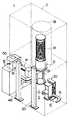
図1に示されているように、本実施の形態に係る拡散CVD方法が実施される拡散CVD装置1は平面視が長方形の直方体の箱形状に形成された筐体2を備えている。筐体2の左側側壁の後部(左右前後は図1を基準とする。)にはクリーンユニット3が設置されており、クリーンユニット3は筐体2の内部にクリーンエアを供給するようになっている。筐体2の内部における後部の略中央には熱処理ステージ4が設定され、熱処理ステージ4の左脇の前後には空のボートを仮置きして待機させる待機ステージ(以下、待機ステージという。)5および処理済みボートを仮置きして冷却するステージ(以下、冷却ステージという。)6が設定されている。筐体2の内部における前部の略中央にはウエハローディングステージ7が設定されており、その手前にはポッドステージ8が設定されている。ウエハローディングステージ7の左脇にはノッチ合わせ装置9が設置されている。以下、各ステージの構成を順に説明する。
【0012】
図5および図6に示されているように、熱処理ステージ4の上部には石英ガラスが使用されて下端が開口した円筒形状に一体成形されたプロセスチューブ11が、中心線が垂直になるように縦に配されている。プロセスチューブ11の筒中空部はボートによって同心的に整列した状態に保持された複数枚のウエハが搬入される処理室12を形成しており、プロセスチューブ11の下端開口は被処理基板としてのウエハを出し入れするための炉口13を構成している。したがって、プロセスチューブ11の内径は取り扱うウエハの最大外径よりも大きくなるように設定されている。
【0013】
プロセスチューブ11の下端面はマニホールド14の上端面にシールリング15を挟んで当接されており、マニホールド14が筐体2に支持されることにより、プロセスチューブ11は垂直に支持された状態になっている。マニホールド14の側壁の一部には排気管16が処理室12に連通するように接続されており、排気管16の他端は処理室12を所定の真空度に真空排気するための真空排気装置(図示せず)に接続されている。マニホールド14の側壁の他の部分にはガス導入管17が処理室12に連通するように接続されており、ガス導入管17の他端は原料ガスや窒素ガス等のガスを供給するためのガス供給装置(図示せず)に接続されている。
【0014】
プロセスチューブ11の外部にはヒータユニット18がプロセスチューブ11を包囲するように同心円に設備されており、ヒータユニット18は筐体2に支持されることにより垂直に据え付けられた状態になっている。ヒータユニット18は処理室12内を全体にわたって均一に加熱するように構成されている。
【0015】
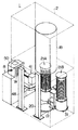
熱処理ステージ4におけるプロセスチューブ11の真下にはプロセスチューブ11の外径と略等しい円盤形状に形成されたキャップ19が同心的に配置されており、キャップ19は送りねじ機構によって構成されたエレベータ20によって垂直方向に昇降されるようになっている。キャップ19は中心線上にボート21を垂直に立脚して支持するようになっている。本実施形態において、ボート21は二台が使用される。
【0016】
図5および図6に示されているように、二台のボート21、21はいずれも、上下で一対の端板22、23と、両端板22、23間に架設されて垂直に配設された複数本(本実施の形態では三本)の保持部材24とを備えており、各保持部材24に長手方向に等間隔に配されて互いに同一平面内において開口するようにそれぞれ刻設された複数条の保持溝25間にウエハWを挿入されることにより、複数枚のウエハWを水平にかつ互いに中心を揃えた状態に整列させて保持するように構成されている。
【0017】
ボート21の下側端板23の下には断熱キャップ部26が形成されており、断熱キャップ部26の下面には断熱キャップ部26の外径よりも小径の円柱形状に形成された支柱27が垂直方向下向きに突設されている。断熱キャップ部26の下面における支柱27の下面には後記するボート移送装置のアームが挿入されるスペースが形成されており、支柱27の下面における外周辺部によってアームを係合するための係合部28が構成されている。支柱27の下面にはベース29が水平に設けられている。
【0018】
図1に示されているように、待機ステージ5と冷却ステージ6との間にはボート21を熱処理ステージ4と待機ステージ5および冷却ステージ6との間で移送するボート移送装置30が設備されている。図7に示されているように、ボート移送装置30はスカラ形ロボット(selective compliance assembly robot arm SCARA)によって構成されており、水平面内で約90度ずつ往復回動する一対の第一アーム31および第二アーム32を備えている。第一アーム31および第二アーム32はいずれも円弧形状に形成されており、ボート21の支柱27の外側に挿入された状態で断熱キャップ部26の係合部28に下から係合することにより、ボート21全体を垂直に支持するようになっている。
【0019】
図1および図7に示されているように、待機ステージ5にはボート21を垂直に支持する待機台33が設置されており、第一アーム31はボート21を待機台33と熱処理ステージ4のキャップ19との間で移送するように構成されている。冷却ステージ6には冷却台34が設置されており、第二アーム32はボート21を冷却台34と熱処理ステージ4のキャップ19との間で移送するように構成されている。
【0020】
図1に示されているように、筐体2内にクリーンエア35を供給するクリーンユニット3はクリーンエア35を待機ステージ5および冷却ステージ6に向けて吹き出すように構成されている。すなわち、図8に示されているように、クリーンユニット3はクリーンエア35を吸い込む吸込ダクト36を備えており、吸込ダクト36の下端部には吸込ファン37が設置されている。吸込ファン37の吐出口側には吹出ダクト38が前後方向に延在するように長く敷設されており、吹出ダクト38の筐体2の内側面における吸込ダクト36の前後の両脇にはクリーンエア35を待機ステージ5および冷却ステージ6にそれぞれ向けて吹き出す吹出口39、39が大きく開設されている。
【0021】
他方、図1に示されているように、筐体2の内部における後側の右隅には排気用ファン40が設置されており、排気用ファン40はクリーンユニット3の吹出口39、39から吹き出されたクリーンエア35を吸い込んで筐体2内の外部に排出するようになっている。
【0022】
図1〜図4に示されているように、ウエハローディングステージ7にはスカラ形ロボットによって構成されたウエハ移載装置41が設置されており、ウエハ移載装置41はウエハWをポッドステージ8と待機ステージ5との間で移送してポッドとボート21との間で移載するように構成されている。
【0023】
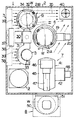
すなわち、図9に示されているように、ウエハ移載装置41はベース42を備えており、ベース42の上面にはベース42に対して旋回するターンテーブル43が設置されている。ターンテーブル43の上にはリニアガイド44が設置されており、リニアガイド44はその上に設置された移動台45を水平移動させるように構成されている。移動台45の上には取付台46が移動台45によって水平移動されるように設置されており、取付台46にはウエハWを下から支持するツィーザ47が複数枚(本実施の形態においては五枚)、等間隔に配置されて水平に取り付けられている。図1〜図4に示されているように、ウエハ移載装置41は送りねじ機構によって構成されたエレベータ48によって昇降されるようになっている。
【0024】
ポッドステージ8にはウエハWを搬送するためのキャリア(収納容器)としてのFOUP(front opning unified pod。以下、ポッドという。)50が一台ずつ載置されるようになっている。ポッド50は一つの面が開口した略立方体の箱形状に形成されており、開口部にはドア51が着脱自在に装着されている。ウエハのキャリアとしてポッドが使用される場合には、ウエハが密閉された状態で搬送されることになるため、周囲の雰囲気にパーティクル等が存在していたとしてもウエハの清浄度は維持することができる。したがって、拡散CVD装置が設置されるクリーンルーム内の清浄度をあまり高く設定する必要がなくなるため、クリーンルームに要するコストを低減することができる。そこで、本実施の形態に係る拡散CVD装置においては、ウエハのキャリアとしてポッド50が使用されている。なお、ポッドステージ8にはポッド50のドア51を開閉するためのドア開閉装置(図示せず)が設置されている。
【0025】
図10は拡散CVD装置の制御システムを示すブロック図である。図10に示されている制御システム60はいずれもコンピュータによって構築されたメインコントローラと複数のサブコントローラとによって構成されている。サブコントローラとしては、処理室の温度を制御する温度制御サブコントローラ61と、処理室の圧力を制御する圧力制御サブコントローラ62と、原料ガスやキャリアガスおよびパージガス等のガス流量を制御するガス制御サブコントローラ63と、各種のエレベータやボート移送装置およびウエハ移載装置等の機械を制御する機械制御サブコントローラ64とが構築されており、これらサブコントローラはメインコントローラ66に制御ネットワーク65によって接続されている。
【0026】
メインコントローラ66には表示手段および入力手段(ユーザ・インタフェース)としてのコンソール(制御卓)67およびレシピ等を記憶する記憶装置68が接続されている。コンソール67はディスプレイとキーボードおよびマウスとを備えており、ディスプレイにレシピの内容(項目名や制御パラメータの数値等)表示するとともに、キーボードやマウスによって作業者の指令を伝達するように構成されている。
【0027】
本実施の形態において、メインコントローラ66にはウエハチャージ(移載)開始時点算出部70が構築(プログラミング)されており、ウエハチャージ開始時点算出部70は後述するウエハチャージ移載開始時点算出方法を実行するように構成されている。
【0028】
以下、前記構成に係る拡散CVD装置を使用した本発明の一実施の形態である拡散CVD処理方法を、一対のボートの運用方法を主体にして図11に示されているタイムチャートに沿って説明する。なお、図11中、K1〜K11は後述する各工程を示しており、t1 〜t11は各工程K1〜K11の各所要時間をそれぞれ示している。
【0029】
以下の拡散CVD処理方法は予め指定された成膜プロセスのレシピを実行する制御シーケンスによって実施されるものであり、指定されたレシピが記憶装置68からメインコントローラ66のRAM等に展開されて、各サブコントローラ62〜64に指令されることにより実施される。
【0030】
まず、図11にK1で示されている第一ボートのウエハチャージ工程において、ポッド50に収納されたウエハWが一対のボート21、21のうちの一方のボート(以下、第一ボート21Aという。)にウエハ移載装置41によって移載(チャージ)される。ウエハチャージ工程K1の所要時間t1 は、ウエハチャージ枚数が150枚の場合には約12分である。
【0031】
ウエハチャージ工程K1において、図1に示されているように、複数枚のウエハWが収納されたポッド50はポッドステージ8に供給され、図2に示されているように、ポッドステージ8に供給されたポッド50はドア51をドア開閉装置によって開放される。他方、図1および図2に示されているように、待機ステージ5の待機台33には第一ボート21Aが載置されて、ウエハチャージ工程K1の実行に待機した状態になっている。
【0032】
そして、図9において、(a)に示された状態から(b)に示されているように、移動台45および取付台46がポッド50の方向に移動されてツィーザ47がポッド50内に挿入され、ポッド50内のウエハWを受け取る。続いて、ツィーザ47は(a)に示された位置に後退する。次に、ターンテーブル43が反転し、移動台45および取付台46が待機ステージ5の方向に移動されて、ツィーザ47が保持したウエハWを第一ボート21Aの保持溝25に受け渡す。ウエハWを第一ボート21Aに移載したウエハ移載装置41は移動台45および取付台46を一度後退させた後に再び反転して、ツィーザ47をポッド50側に向けた図9(a)の状態になる。
【0033】
この際、ウエハ移載装置41は五枚のツィーザ47を備えているため、一回の移載作動で五枚のウエハWをポッド50の五段の保持溝から第一ボート21Aの五段の保持溝25に移載することができる。ここで、第一ボート21Aがバッチ処理するウエハWの枚数(本実施の形態においては、150枚)は、一台のポッド50に収納されたウエハWの枚数(同じく25枚)よりも多いため、ウエハ移載装置41は複数台のポッド50から所定枚数のウエハWを第一ボート21Aにエレベータ48によって昇降されて移載することになる。
【0034】
次いで、図11にK2で示されているボート移送工程が実施される。ボート移送工程K2の所要時間t2 は約0.5分である。
【0035】
ボート移送工程K2において、待機ステージ5にて指定の枚数のウエハWを移載された第一ボート21Aは、待機ステージ5から熱処理ステージ4へボート移送装置30の第一アーム31によって図4に示されているように移送され、キャップ19の上に移送される。すなわち、第一アーム31は第一ボート21Aの支柱27の外側に挿入して断熱キャップ部26の係合部28に下から係合することによって第一ボート21Aを垂直に支持した状態で、約90度回動することによって、第一ボート21Aを待機ステージ5から熱処理ステージ4へ移送しキャップ19の上に受け渡す。そして、第一ボート21Aをキャップ19に移載した第一アーム31は待機ステージ5に戻る。
【0036】
次に、図11にK3で示されているボート搬入工程が実施される。ボート搬入工程K3の所要時間t3 は約2分である。
【0037】
ボート搬入工程K3においては、図5に示されているように、キャップ19に垂直に支持された第一ボート21Aはエレベータ20によって上昇されてプロセスチューブ11の処理室12に搬入される。第一ボート21Aが上限に達すると、キャップ19の上面の外周辺部がマニホールド14の下面にシールリング15を挟んで着座した状態になってマニホールド14の下端開口をシール状態に閉塞するため、処理室12は気密に閉じられた状態になる。
【0038】
処理室12がキャップ19によって気密に閉じられると、図11にK4で示されている昇温・温度安定工程が実施される。すなわち、処理室12が所定の真空度に排気管16によって真空排気され、ヒータユニット18によって所定の処理温度(例えば、800〜1000℃)をもって全体にわたって均一に加熱される。
【0039】
処理室12の温度が安定すると、図11にK5で示されている成膜工程が実施される。すなわち、成膜工程K5において、処理ガスが処理室12にガス導入管17を通じて所定の流量供給される。これによって、所定の成膜処理が施される。
【0040】
所定の成膜処理が終了すると、図11にK6で示されている窒素(N2 )ガスパージ工程が実施される。すなわち、窒素ガスパージ工程K6において、窒素ガスがガス導入管17を通じて所定の流量および時間(t6 )だけ供給されて処理室12が窒素ガスで置き換えられるとともに温度が下げられる。
【0041】
そして、取り扱う膜種によって異なるが、昇温・温度安定工程K4、成膜工程K5および窒素ガスパージ工程K6の所要時間(t4 +t5 +t6 )は約1時間〜2時間である。つまり、いずれの膜種にせよ、昇温・温度安定工程K4、成膜工程K5および窒素ガスパージ工程K6の所要時間(t4 +t5 +t6 )は、ウエハチャージ工程K1の所要時間t1 の約12分に比べて遙に長期間になる。
【0042】
なお、この第一ボート21Aの熱処理の間に、一対のボート21、21の他方のボート(以下、第二ボート21Bという。)が待機ステージ5の待機台33の上に移送されて待機した状態になっている。
【0043】
その後、図11にK7で示されているボート搬出工程が実施される。ボート搬出工程K7の所要時間t7 は約2分である。
【0044】
すなわち、ボート搬出工程K7においては、図6に示されているように、第一ボート21Aを支持したキャップ19がエレベータ20によって下降されて、第一ボート21Aがプロセスチューブ11の処理室12から搬出される。第一ボート21Aが搬出されたプロセスチューブ11の処理室12の炉口13はシャッタ(図示せず)によって閉鎖され、処理室12の高温雰囲気が逃げるのを防止される。処理室12から搬出された第一ボート21A(保持されたウエハW群を含む)は高温の状態になっている。
【0045】
続いて、図11にK8で示されているボート移送工程が実施されて、高温状態の第一ボート21Aが熱処理ステージ4から冷却ステージ6に移送される。ボート移送工程K8の所要時間t8 は約0.5分である。
【0046】
すなわち、図3に示されているように、処理室12から搬出された高温状態の処理済みの第一ボート21Aはプロセスチューブ11の軸線上の熱処理ステージ4から冷却ステージ6へ、ボート移送装置30の第二アーム32によって直ちに移送されて仮置きされる。この際、第二アーム32は処理済みの第一ボート21Aの支柱27の外側に挿入して断熱キャップ部26の係合部28に下から係合することによって処理済みの第一ボート21Aを垂直に支持した状態で、約90度回動することにより、処理済みの第一ボート21Aを熱処理ステージ4のキャップ19の上から冷却ステージ6の冷却台34の上へ移送し載置する。
【0047】
冷却ステージ6の冷却台34に移載された高温状態の処理済み第一ボート21Aは、図11にK9で示されている冷却工程を実施される。冷却工程K9の所要時間t9 は約10分である。
【0048】
冷却工程K9において、図4に示されているように、冷却ステージ6はクリーンユニット3のクリーンエア吹出口39の近傍に設定されているため、冷却ステージ6の冷却台34に移載された高温状態の第一ボート21Aはクリーンユニット3の吹出口39から吹き出すクリーンエア35によってきわめて効果的に冷却される。この際、図4に示されているように、クリーンユニット3の吹出口39から吹き出したクリーンエア35の流れは、吹出口39から見ると待機ステージ5とは反対方向である筐体2の後部右隅に配置された排気用ファン40に向かうため、熱処理ステージ4および待機ステージ5の方向には向かわない。したがって、処理済みの第一ボート21Aに接触したクリーンエア35が熱処理ステージ4および待機ステージ5に流れることにより、熱処理ステージ4および待機ステージ5の第二ボート21Bに保持されたウエハW群を汚染することは防止することができる。
【0049】
その後、冷却台34の第一ボート21Aは図11にK10で示されているボート移送工程を実施される。ボート移送工程K10の所要時間t7 は約0.5分である。ボート移送工程K10は次のように実行される。この際、処理済みの第一ボート21Aは充分に冷却されて、例えば、150℃以下になっている。
【0050】
すなわち、ボート移送装置30の第二アーム32は第一ボート21Aの支柱27の外側に挿入して断熱キャップ部26の係合部28に下から係合することによって第一ボート21Aを垂直に支持した状態で、約90度回動することにより、第一ボート21Aを冷却ステージ6から熱処理ステージ4へ移送する。第一ボート21Aが熱処理ステージ4に移送されると、ボート移送装置30の第一アーム31が約90度回転されて熱処理ステージ4に移動され、熱処理ステージ4の第一ボート21Aを受け取る。第一ボート21Aを受け取ると、第一アーム31は元の方向に約90度逆回転して第一ボート21Aを熱処理ステージ4から待機ステージ5に移送して、待機台33に移載する。待機台33に移載された状態において、第一ボート21Aの三本の保持部材24はウエハ移載装置41側が開放した状態になる。
【0051】
次に、図11にK11で示されているディスチャージ工程がウエハ移載装置40によって実施される。ディスチャージ工程K11の所要時間t11は約12分である。ディスチャージ工程K11は図7について前述した作動に準ずるウエハ移載装置41の作動により実施される。
【0052】
すなわち、ウエハ移載装置41は待機ステージ5の第一ボート21Aから処理済みのウエハWを受け取ってポッドステージ8のポッド50に移載して行く。この際、第一ボート21Aがバッチ処理した処理済みウエハWの枚数は一台のポッド50に収納されるウエハWの枚数よりも多いため、ウエハ移載装置41はエレベータ48によって昇降されながら、ポッドステージ8に入れ換えられる複数台のポッド50にウエハWを所定枚数ずつ収納して行くことになる。
【0053】
全ての処理済みウエハWがポッド50に戻されると、待機台33の上の第一ボート21Aには、次に処理すべき新規のウエハWがウエハ移載装置41によって移載(チャージ)されて行くウエハチャージ工程K1が、実行されることになる。但し、本実施の形態に係る拡散CVD処理方法においては、ウエハチャージ工程K1は後述するウエハチャージ開始時点算出方法よって算出されたタイミングをもって開始されることになる。これは第二ボート21Bについても同様である。
【0054】
以降、前述した作用が第一ボート21Aと第二ボート21Bとの間で交互に繰り返されることにより、多数枚のウエハWが拡散CVD装置1によってバッチ処理されて行く。
【0055】
ところで、ディスチャージ工程K11が完了した後に続いてウエハチャージ工程K1が実施される従来例の場合には、ウエハチャージ工程K1を実施された一方のボート(第一ボートまたは第二ボート)に移載の新規ウエハ群は熱処理ステージ4での他方のボート(第一ボートまたは第二ボート)の処理が終了するまでの約1時間〜2時間の長期間にわたって大気雰囲気の待機ステージ5において待機することになる。このように新規のウエハ群が大気雰囲気中に長期間晒されると、自然酸化膜がこれから処理しようとするウエハWの表面に大気中の酸素や水分によって形成されてしまう。
【0056】
そこで、本実施の形態においては、ウエハチャージ工程K1の開始時点の最適値をウエハチャージ開始時点算出方法によって求め、算出されたタイミングをもってウエハチャージ工程K1を開始することにより、大気雰囲気の待機ステージ5での待機時間を最も短縮するものとする。
【0057】
次に、本実施の形態に係るウエハチャージ開始時点算出方法を図12について説明する。なお、図12に示されているフローはメインコントローラ66のウエハチャージ開始時点算出部70において実行される。
【0058】
図12にS1で示されている第一ステップにおいて、第一ボートのボート搬出工程K7迄の累積時間が算出される。すなわち、累積時間をTとすると、累積時間は、T=t1 +t2 +t3 +t4 +t5 +t6 +t7 、によって求められる。なお、t1 〜t7 は前記各工程K1〜K7の所要時間である。
【0059】
次に、図12にS2で示されている第二ステップにおいて、「第一ボートのボート搬出工程K7迄の累積時間か」が判断される。累積時間でない場合(NO)には、第一ステップS1に戻り、第一ステップS1と第二ステップS2とが繰り返される。累積時間である場合(YES)には第三ステップS3に進む。
【0060】
第三ステップS3において、第二ボートのウエハチャージ開始時点T’が算出される。すなわち、ウエハチャージ開始時点T’は、T’=T−t1 、によって求められる。
【0061】
以上のようにして算出されたウエハチャージ開始時点に基づいて、メインコントローラ66は図13に示されているフローを実行する。
【0062】
すなわち、図13に示されている第一ステップP1において、「レシピの実行時間が第二ボートへのウエハチャージ開始時点になったか」を判断する。開始時点になっていない場合(NO)には、第一ステップP1を繰り返し、開始時点になっている場合(YES)には第二ステップP2に進む。
【0063】
第二ステップP2において、第二ボートへのウエハチャージ工程K1を開始する。なお、以上の説明では第二ボートのウエハチャージ工程K1の開始時点を算出して実行する場合について述べたが、第一ボートと第二ボートとは交互に同じように運用されるため、第一ボートについても同様に算出されて実行される。
【0064】
本実施の形態によれば、ウエハチャージ開始時点の最適値を予め求めて、次の処理に待機するウエハの待機時間を最小に短縮することにより、ウエハが大気雰囲気に晒される時間を最小限度に抑制することができるため、ウエハの表面に形成される自然酸化膜の増加を抑制することができる。
【0065】
例えば、ウエハチャージ工程K1の所要時間t1 がウエハ150枚で約12分、ボート搬出工程K7の所要時間t7 とボート移送工程K8の所要時間t8 との合計所要時間t7 +t8 が約4分、ボート移送工程K2の所要時間t2 が0.5分であると、待機中のウエハWが大気雰囲気に晒される時間は、約16.5分となる。
【0066】
ここで、図14は大気雰囲気に晒されたウエハの表面における自然酸化膜の増加特性を示すグラフである。図14によれば、約16.5分における自然酸化膜の厚さは、1Å以下、になる。この程度の厚さの自然酸化膜はウエハに処理される膜厚のばらつきに影響を及ぼしたり、接触抵抗を増加させたりすることはないため、ICの高集積化や品質(精度等)、性能(演算速度等)および信頼性に対して悪影響を及ぼすことは未然に防止することができる。
【0067】
なお、本発明は前記実施の形態に限定されるものではなく、その要旨を逸脱しない範囲で種々に変更が可能であることはいうまでもない。
【0068】
例えば、第二ボートへのウエハチャージ工程の終了は第一ボートの搬出工程前迄に終了するように設定するに限らず、第一ボートのボート移送工程を完了する直前までに第二ボートへのウエハチャージ工程を終了させるように設定してもよい。この場合には、ウエハが大気雰囲気に晒される時間をより一層短縮することができるため、自然酸化膜の増加をより一層低減することができる。
【0069】
筐体に供給する気体はクリーンエアに限らず、窒素ガス等の不活性ガスであってもよい。
【0070】
拡散CVD装置はアニール処理や酸化膜形成処理、拡散処理および成膜処理等の熱処理全般に使用することができる。
【0071】
本実施の形態ではバッチ式縦形ホットウオール形拡散CVD装置を使用する場合について説明したが、本発明はこれに限らず、バッチ式横形ホットウオール形拡散CVD装置等の基板処理方法全般に適用することができる。
【0072】
前記実施の形態ではウエハに熱処理が施される場合について説明したが、被処理基板はホトマスクやプリント配線基板、液晶パネル、コンパクトディスクおよび磁気ディスク等であってもよい。
【0073】
【発明の効果】
以上説明したように、本発明によれば、ウエハが大気雰囲気に晒される時間を短縮することができる。
【図面の簡単な説明】
【図1】本発明の一実施の形態である拡散CVD処理方法に使用される拡散CVD装置を示す平面断面図である。
【図2】その斜視図である。
【図3】処理済みボートの冷却中を示す斜視図である。
【図4】同じく平面断面図である。
【図5】熱処理ステージの処理中を示す縦断面図である。
【図6】同じくボート搬出後を示す縦断面図である。
【図7】ボート移送装置を示す斜視図である。
【図8】クリーンユニットを示す斜視図である。
【図9】ウエハ移載装置を示す各側面図であり、(a)は短縮時を示し、(b)は伸長時を示している。
【図10】制御システムを示すブロック図である。
【図11】拡散CVD処理方法を示すタイムチャートである。
【図12】ウエハチャージ開始時点算出方法を示すフローチャートである。
【図13】ウエハチャージ開始時点の実行フローを示すフローチャートである。
【図14】大気雰囲気に晒されたウエハの表面における自然酸化膜の増加特性を示すグラフである。
【符号の説明】
W…ウエハ(基板)、1…拡散CVD装置(基板処理装置)、2…筐体、3…クリーンユニット、4…熱処理ステージ、5…待機ステージ、6…冷却ステージ、7…ウエハローディングステージ、8…ポッドステージ、9…ノッチ合わせ装置、11…プロセスチューブ、12…処理室、13…炉口、14…マニホールド、15…シールリング、16…排気管、17…ガス導入管、18…ヒータユニット、19…キャップ、20…エレベータ、21…ボート、21A…第一ボート、21B…第二ボート、22…上側端板、23…下側端板、24…保持部材、25…保持溝、26…断熱キャップ部、27…支柱、28…係合部、29…ベース、30…ボート移送装置、31…第一アーム、32…第二アーム、33…待機台、34…冷却台、35…クリーンエア、36…吸込ダクト、37…吸込ファン、38…吹出ダクト、39…吹出口、40…排気用ファン、41…ウエハ移載装置、42…ベース、43…ターンテーブル、44…リニアガイド、45…移動台、46…取付台、47…ツィーザ、48…エレベータ、50…ポッド、51…ドア、60…制御システム、61…温度制御サブコントローラ、62…圧力制御サブコントローラ、63…ガス制御サブコントローラ、64…機械制御サブコントローラ、65…制御ネットワーク、66…メインコントローラ、67…コンソール(制御卓)、68…記憶装置、70…ウエハチャージ開始時点算出部。[0001]
BACKGROUND OF THE INVENTION
The present invention relates to a substrate processing method, and more particularly to technology for preventing oxidation and contamination of a substrate to be processed. For example, in a semiconductor device manufacturing process, an annealing process, an oxide film forming process, a diffusion process, and a film forming process on a semiconductor wafer. The present invention relates to an effective material that can be used for heat treatment such as treatment.
[0002]
In general, a batch type vertical hot wall heat treatment apparatus (furnace) is used to perform heat treatment such as annealing, oxide film formation, diffusion and film formation on a semiconductor wafer (hereinafter referred to as a wafer) in a semiconductor device manufacturing process. Hereinafter, the heat treatment apparatus is widely used.
[0003]
As a conventional heat treatment apparatus of this kind, there is one described in Japanese Patent No. 2681055. In this heat treatment apparatus, a boat exchange device is disposed between the wafer transfer device and the space immediately below the process tube, and a pair (two) of boats are placed on the rotary table of the boat exchange device, A pair of boats rotate 180 degrees around the rotary table, whereby an unprocessed boat and a processed boat are exchanged. That is, in this heat treatment apparatus, while one boat (first boat) holding a wafer group is being processed in the process chamber of the process tube, a new wafer is transferred to the other boat (second boat). It is transferred by a loading device.
[0004]
[Problems to be solved by the invention]
In general, the film formation time of the heat treatment apparatus is 1 to 2 hours, although it depends on the type of film processed by the heat treatment apparatus. On the other hand, the time required to transfer a new wafer onto the boat by the wafer transfer device is about 12 minutes for 150 wafers. Therefore, in the above-described heat treatment apparatus, the new wafer group transferred to the second boat waits outside the processing chamber for a long period of about 1 to 2 hours until the processing of the first boat is completed. become.
[0005]
However, when a new wafer group transferred to the second boat is exposed to the atmospheric air outside the processing chamber for a long period of time, an oxide film (hereinafter referred to as a natural oxide film) unintentionally controlled is exposed to the atmosphere on the wafer surface. It is formed by oxygen and moisture. Since this natural oxide film affects the variation in the film thickness processed on the wafer and increases the contact resistance, a semiconductor integrated circuit device (hereinafter referred to as an IC) manufactured by the wafer is highly integrated. It adversely affects quality (accuracy, lifetime, etc.), performance (calculation speed, etc.) and reliability.
[0006]
An object of the present invention is to provide a substrate processing method capable of reducing the standby time in the air atmosphere and preventing the generation of a natural oxide film.
[0007]
[Means for Solving the Problems]
The substrate processing method according to the present invention includes a process tube in which a processing chamber is formed, a boat that enters and exits the processing chamber and carries a plurality of substrates in and out, and the processing chamber that receives the plurality of substrates from the boat. A substrate processing method in which a substrate processing apparatus including a substrate transfer apparatus that receives and transfers outside is used, wherein at least two boats are sequentially used.
The substrate transfer time by the substrate transfer device to the other boat to be processed next to the one boat being processed is the substrate transfer time to the other boat and the one boat. It is calculated based on the processing elapsed time.
[0008]
According to the above-mentioned means, since the substrate transfer start time to the boat is automatically determined according to the processing elapsed time, the waiting time of the substrate in the air atmosphere can be set to the shortest. Generation of an oxide film can be prevented.
[0009]
DETAILED DESCRIPTION OF THE INVENTION
Hereinafter, an embodiment of the present invention will be described with reference to the drawings.
[0010]
In the present embodiment, the substrate processing method according to the present invention is carried out using a batch type vertical hot wall diffusion / CVD apparatus (hereinafter referred to as diffusion CVD apparatus) shown in FIG. It is configured and used for performing diffusion and CVD processes such as annealing, oxide film formation, diffusion and film formation on a wafer as a substrate.
[0011]
As shown in FIG. 1, a
[0012]
As shown in FIGS. 5 and 6, the process tube 11 integrally formed in a cylindrical shape using quartz glass at the upper part of the
[0013]
The lower end surface of the process tube 11 is in contact with the upper end surface of the
[0014]
A
[0015]
A
[0016]
As shown in FIGS. 5 and 6, the two
[0017]
A heat insulating
[0018]
As shown in FIG. 1, a
[0019]
As shown in FIGS. 1 and 7, the
[0020]
As shown in FIG. 1, the
[0021]
On the other hand, as shown in FIG. 1, an
[0022]
As shown in FIGS. 1 to 4, a
[0023]
That is, as shown in FIG. 9, the
[0024]
On the
[0025]
FIG. 10 is a block diagram showing a control system of the diffusion CVD apparatus. The control system 60 shown in FIG. 10 is composed of a main controller constructed by a computer and a plurality of sub-controllers. The sub-controller includes a temperature control sub-controller 61 that controls the temperature of the processing chamber, a pressure control sub-controller 62 that controls the pressure of the processing chamber, and a gas control sub-control that controls the gas flow rate of source gas, carrier gas, purge gas, and the like. A controller 63 and a machine control sub-controller 64 for controlling machines such as various elevators, boat transfer devices, and wafer transfer devices are constructed. These sub-controllers are connected to the main controller 66 by a control network 65. .
[0026]
A console (control console) 67 as a display means and input means (user interface) and a storage device 68 for storing recipes and the like are connected to the main controller 66. The console 67 includes a display, a keyboard, and a mouse. The console 67 is configured to display recipe contents (item names, numerical values of control parameters, and the like) on the display, and to transmit operator commands using the keyboard and mouse. .
[0027]
In the present embodiment, a wafer charge (transfer) start
[0028]
Hereinafter, a diffusion CVD processing method according to an embodiment of the present invention using the diffusion CVD apparatus according to the above configuration will be described with reference to a time chart shown in FIG. To do. In FIG. 11, K1 to K11 indicate steps described later, and t 1 ~ T 11 Indicates respective required times of the respective steps K1 to K11.
[0029]
The following diffusion CVD processing method is performed by a control sequence for executing a recipe of a film formation process designated in advance. The designated recipe is expanded from the storage device 68 to the RAM of the main controller 66, and the like. This is implemented by commanding the sub-controllers 62-64.
[0030]
First, in the wafer charging process of the first boat shown by K1 in FIG. 11, the wafer W accommodated in the
[0031]
In the wafer charging step K1, as shown in FIG. 1, the
[0032]
Then, in FIG. 9, from the state shown in (a), as shown in (b), the moving
[0033]
At this time, since the
[0034]
Next, a boat transfer process indicated by K2 in FIG. 11 is performed. Required time t for boat transfer process K2 2 Is about 0.5 minutes.
[0035]
In the boat transfer process K2, the
[0036]
Next, a boat carrying-in process indicated by K3 in FIG. 11 is performed. Required time t for boat loading process K3 Three Is about 2 minutes.
[0037]
In the boat carrying-in process K3, as shown in FIG. 5, the
[0038]
When the
[0039]
When the temperature of the
[0040]
When the predetermined film forming process is completed, nitrogen (N 2 ) A gas purge step is performed. That is, in the nitrogen gas purge step K6, the nitrogen gas flows through the
[0041]
Depending on the type of film to be handled, the required time (t Four + T Five + T 6 ) Is about 1 to 2 hours. That is, for any film type, the time required for the temperature rise / temperature stabilization process K4, the film formation process K5, and the nitrogen gas purge process K6 (t Four + T Five + T 6 ) Is the time t required for the wafer charging process K1. 1 Compared to about 12 minutes, it takes a long time.
[0042]
During the heat treatment of the
[0043]
Thereafter, a boat unloading process indicated by K7 in FIG. 11 is performed. Required time t for boat unloading process K7 7 Is about 2 minutes.
[0044]
That is, in the boat unloading step K7, as shown in FIG. 6, the
[0045]
Subsequently, a boat transfer process indicated by K8 in FIG. 11 is performed, and the
[0046]
That is, as shown in FIG. 3, the high-temperature processed
[0047]
The high-temperature processed
[0048]
In the cooling step K9, as shown in FIG. 4, since the
[0049]
Thereafter, the
[0050]
That is, the
[0051]
Next, the discharge process indicated by K11 in FIG. Time required t for the discharge process K11 11 Is about 12 minutes. The discharge process K11 is performed by the operation of the
[0052]
That is, the
[0053]
When all the processed wafers W are returned to the
[0054]
Thereafter, the above-described operation is alternately repeated between the
[0055]
By the way, in the case of the conventional example in which the wafer charging process K1 is subsequently performed after the completion of the discharging process K11, the wafer is transferred to one boat (the first boat or the second boat) in which the wafer charging process K1 is performed. The new wafer group waits in the
[0056]
Therefore, in the present embodiment, the optimum value at the start time of the wafer charge process K1 is obtained by the wafer charge start time calculation method, and the wafer charge process K1 is started at the calculated timing, whereby the
[0057]
Next, a wafer charge start time calculation method according to the present embodiment will be described with reference to FIG. The flow shown in FIG. 12 is executed by the wafer charge start
[0058]
In the first step indicated by S1 in FIG. 12, the accumulated time until the boat unloading process K7 of the first boat is calculated. That is, if the cumulative time is T, the cumulative time is T = t 1 + T 2 + T Three + T Four + T Five + T 6 + T 7 Sought by. T 1 ~ T 7 Is the time required for each of the steps K1 to K7.
[0059]
Next, in the second step indicated by S2 in FIG. 12, it is determined whether or not "the accumulated time until the boat unloading process K7 of the first boat". If it is not the accumulated time (NO), the process returns to the first step S1, and the first step S1 and the second step S2 are repeated. If it is the accumulated time (YES), the process proceeds to the third step S3.
[0060]
In the third step S3, the wafer charging start time T ′ of the second boat is calculated. That is, the wafer charge start time T ′ is T ′ = T−t. 1 Sought by.
[0061]
Based on the wafer charge start time calculated as described above, the main controller 66 executes the flow shown in FIG.
[0062]
That is, in the first step P1 shown in FIG. 13, it is determined whether or not “the recipe execution time has reached the start time of wafer charge to the second boat”. When it is not the start time (NO), the first step P1 is repeated, and when it is the start time (YES), the process proceeds to the second step P2.
[0063]
In the second step P2, the wafer charging process K1 for the second boat is started. In the above description, the case where the start time of the wafer charging process K1 for the second boat is calculated and executed has been described. However, since the first boat and the second boat are operated in the same manner, A boat is similarly calculated and executed.
[0064]
According to the present embodiment, the optimum value at the time of starting the wafer charge is obtained in advance, and the waiting time of the wafer waiting for the next processing is shortened to the minimum, thereby minimizing the time that the wafer is exposed to the air atmosphere. Since it can suppress, the increase of the natural oxide film formed on the surface of a wafer can be suppressed.
[0065]
For example, the required time t of the wafer charging process K1 1 Is about 12 minutes for 150 wafers, and the required time t for boat unloading process K7 7 And required time t of boat transfer process K8 8 Total time t with 7 + T 8 Is about 4 minutes, required time t for boat transfer process K2. 2 Is 0.5 minutes, the time during which the waiting wafer W is exposed to the air atmosphere is about 16.5 minutes.
[0066]
Here, FIG. 14 is a graph showing the increase characteristic of the natural oxide film on the surface of the wafer exposed to the air atmosphere. According to FIG. 14, the thickness of the natural oxide film in about 16.5 minutes is 1 mm or less. A natural oxide film of this level does not affect the variation in the film thickness processed on the wafer or increase the contact resistance, so IC integration, quality (accuracy, etc.) and performance An adverse effect on (computation speed, etc.) and reliability can be prevented in advance.
[0067]
Needless to say, the present invention is not limited to the above-described embodiment, and various modifications can be made without departing from the scope of the invention.
[0068]
For example, the completion of the wafer charging process to the second boat is not limited to be set to be completed before the first boat unloading process, but to the second boat immediately before completing the boat transfer process of the first boat. You may set so that a wafer charge process may be complete | finished. In this case, since the time for which the wafer is exposed to the air atmosphere can be further shortened, an increase in the natural oxide film can be further reduced.
[0069]
The gas supplied to the housing is not limited to clean air, and may be an inert gas such as nitrogen gas.
[0070]
The diffusion CVD apparatus can be used for heat treatments such as annealing, oxide film formation, diffusion, and film formation.
[0071]
In this embodiment, the case of using a batch type vertical hot wall type diffusion CVD apparatus has been described. However, the present invention is not limited to this, and is applicable to all substrate processing methods such as a batch type horizontal hot wall type diffusion CVD apparatus. Can do.
[0072]
In the above embodiment, the case where the wafer is subjected to the heat treatment has been described. However, the substrate to be processed may be a photomask, a printed wiring board, a liquid crystal panel, a compact disk, a magnetic disk, or the like.
[0073]
【The invention's effect】
As described above, according to the present invention, the time during which the wafer is exposed to the air atmosphere can be shortened.
[Brief description of the drawings]
FIG. 1 is a plan sectional view showing a diffusion CVD apparatus used in a diffusion CVD processing method according to an embodiment of the present invention.
FIG. 2 is a perspective view thereof.
FIG. 3 is a perspective view showing that a processed boat is being cooled.
FIG. 4 is a plan sectional view of the same.
FIG. 5 is a longitudinal sectional view showing the heat treatment stage during processing.
FIG. 6 is a longitudinal sectional view showing the same after the boat is carried out.
FIG. 7 is a perspective view showing a boat transfer device.
FIG. 8 is a perspective view showing a clean unit.
FIGS. 9A and 9B are side views showing the wafer transfer apparatus, wherein FIG. 9A shows a shortened state and FIG. 9B shows an extended state.
FIG. 10 is a block diagram showing a control system.
FIG. 11 is a time chart showing a diffusion CVD processing method.
FIG. 12 is a flowchart showing a method for calculating a wafer charge start time.
FIG. 13 is a flowchart showing an execution flow at the start of wafer charging.
FIG. 14 is a graph showing an increase characteristic of a natural oxide film on the surface of a wafer exposed to an air atmosphere.
[Explanation of symbols]
W: Wafer (substrate), 1 ... Diffusion CVD apparatus (substrate processing apparatus), 2 ... Housing, 3 ... Clean unit, 4 ... Heat treatment stage, 5 ... Standby stage, 6 ... Cooling stage, 7 ... Wafer loading stage, 8 Pod stage, 9 notch aligner, 11 process tube, 12 processing chamber, 13 furnace opening, 14 manifold, 15 seal ring, 16 exhaust pipe, 17 gas introduction pipe, 18 heater unit, DESCRIPTION OF
Claims (2)
前記処理室での処理が終了し該処理室から搬出されたボートを前記ステージに移送するステップが完了する直前に前記ボートの次に処理される他のボートへの前記基板移載装置による前記基板の移載ステップを終了させるように設定されることを特徴とする半導体装置の製造方法。A process tube in which a processing chamber is formed; a boat that enters and exits the processing chamber to load and unload a plurality of substrates; and a substrate transfer device that transfers the plurality of substrates to and from the boat outside the processing chamber. And a stage for temporarily placing the boat outside the processing chamber, in a method for manufacturing a semiconductor device in which at least two boats are used sequentially,
The substrate by the substrate transfer apparatus to another boat processed next to the boat immediately before the step of transferring the boat carried out of the processing chamber to the stage after the processing in the processing chamber is completed is completed. A method of manufacturing a semiconductor device, wherein the transfer step is set to be completed .
Priority Applications (1)
| Application Number | Priority Date | Filing Date | Title |
|---|---|---|---|
| JP2000157939A JP4456727B2 (en) | 2000-05-29 | 2000-05-29 | Semiconductor device manufacturing method and substrate processing apparatus |
Applications Claiming Priority (1)
| Application Number | Priority Date | Filing Date | Title |
|---|---|---|---|
| JP2000157939A JP4456727B2 (en) | 2000-05-29 | 2000-05-29 | Semiconductor device manufacturing method and substrate processing apparatus |
Publications (3)
| Publication Number | Publication Date |
|---|---|
| JP2001338889A JP2001338889A (en) | 2001-12-07 |
| JP2001338889A5 JP2001338889A5 (en) | 2007-07-12 |
| JP4456727B2 true JP4456727B2 (en) | 2010-04-28 |
Family
ID=18662484
Family Applications (1)
| Application Number | Title | Priority Date | Filing Date |
|---|---|---|---|
| JP2000157939A Expired - Lifetime JP4456727B2 (en) | 2000-05-29 | 2000-05-29 | Semiconductor device manufacturing method and substrate processing apparatus |
Country Status (1)
| Country | Link |
|---|---|
| JP (1) | JP4456727B2 (en) |
Families Citing this family (2)
| Publication number | Priority date | Publication date | Assignee | Title |
|---|---|---|---|---|
| JP5027430B2 (en) * | 2006-03-07 | 2012-09-19 | 株式会社日立国際電気 | Substrate processing equipment |
| JP4880408B2 (en) * | 2006-09-22 | 2012-02-22 | 株式会社日立国際電気 | Substrate processing apparatus, substrate processing method, semiconductor device manufacturing method, main controller, and program |
-
2000
- 2000-05-29 JP JP2000157939A patent/JP4456727B2/en not_active Expired - Lifetime
Also Published As
| Publication number | Publication date |
|---|---|
| JP2001338889A (en) | 2001-12-07 |
Similar Documents
| Publication | Publication Date | Title |
|---|---|---|
| US7198447B2 (en) | Semiconductor device producing apparatus and producing method of semiconductor device | |
| JP6688850B2 (en) | Substrate processing apparatus, semiconductor device manufacturing method, and program | |
| US20110179717A1 (en) | Substrate processing apparatus | |
| JP2010103545A (en) | Substrate processing apparatus | |
| JP5545795B2 (en) | Substrate processing apparatus and semiconductor manufacturing apparatus management method | |
| JP2002203892A (en) | Apparatus for processing substrate, method for processing substrate and method for manufacturing semiconductor device | |
| TWI752520B (en) | Substrate processing apparatus and manufacturing method of semiconductor device | |
| JP2001284276A (en) | Substrate treating device | |
| JP4456727B2 (en) | Semiconductor device manufacturing method and substrate processing apparatus | |
| KR20210127738A (en) | Semiconductor device manufacturing method, substrate processing apparatus and program | |
| JP4880408B2 (en) | Substrate processing apparatus, substrate processing method, semiconductor device manufacturing method, main controller, and program | |
| JP4383636B2 (en) | Semiconductor manufacturing apparatus and semiconductor device manufacturing method | |
| JP4283973B2 (en) | Substrate processing apparatus and semiconductor device manufacturing method | |
| JP2004119627A (en) | Semiconductor device manufacturing apparatus | |
| JP2003100736A (en) | Substrate treatment apparatus | |
| JP4194262B2 (en) | Substrate processing apparatus and substrate processing method | |
| KR20230130775A (en) | Processing apparatus, exhaust system and method of manufacturing semiconductor device | |
| JP4224192B2 (en) | Manufacturing method of semiconductor device | |
| US20200291516A1 (en) | Substrate processing apparatus | |
| JP2004023032A (en) | Manufacturing apparatus for semiconductor | |
| JP2004128390A (en) | Substrate processing device | |
| JP2007194481A (en) | Substrate treatment apparatus | |
| JP2002009000A (en) | Semiconductor manufacturing device | |
| JP2001284277A (en) | Substrate treating device | |
| JP2001284278A (en) | Device and method for treating substrate |
Legal Events
| Date | Code | Title | Description |
|---|---|---|---|
| A521 | Written amendment |
Free format text: JAPANESE INTERMEDIATE CODE: A523 Effective date: 20070528 |
|
| A621 | Written request for application examination |
Free format text: JAPANESE INTERMEDIATE CODE: A621 Effective date: 20070528 |
|
| A977 | Report on retrieval |
Free format text: JAPANESE INTERMEDIATE CODE: A971007 Effective date: 20091105 |
|
| A131 | Notification of reasons for refusal |
Free format text: JAPANESE INTERMEDIATE CODE: A131 Effective date: 20091110 |
|
| A521 | Written amendment |
Free format text: JAPANESE INTERMEDIATE CODE: A523 Effective date: 20100105 |
|
| TRDD | Decision of grant or rejection written | ||
| A01 | Written decision to grant a patent or to grant a registration (utility model) |
Free format text: JAPANESE INTERMEDIATE CODE: A01 Effective date: 20100202 |
|
| A01 | Written decision to grant a patent or to grant a registration (utility model) |
Free format text: JAPANESE INTERMEDIATE CODE: A01 |
|
| A61 | First payment of annual fees (during grant procedure) |
Free format text: JAPANESE INTERMEDIATE CODE: A61 Effective date: 20100208 |
|
| FPAY | Renewal fee payment (event date is renewal date of database) |
Free format text: PAYMENT UNTIL: 20130212 Year of fee payment: 3 |
|
| R150 | Certificate of patent or registration of utility model |
Ref document number: 4456727 Country of ref document: JP Free format text: JAPANESE INTERMEDIATE CODE: R150 Free format text: JAPANESE INTERMEDIATE CODE: R150 |
|
| FPAY | Renewal fee payment (event date is renewal date of database) |
Free format text: PAYMENT UNTIL: 20130212 Year of fee payment: 3 |
|
| FPAY | Renewal fee payment (event date is renewal date of database) |
Free format text: PAYMENT UNTIL: 20140212 Year of fee payment: 4 |
|
| S111 | Request for change of ownership or part of ownership |
Free format text: JAPANESE INTERMEDIATE CODE: R313111 |
|
| S531 | Written request for registration of change of domicile |
Free format text: JAPANESE INTERMEDIATE CODE: R313531 |
|
| R350 | Written notification of registration of transfer |
Free format text: JAPANESE INTERMEDIATE CODE: R350 |
|
| EXPY | Cancellation because of completion of term |