JP4446292B2 - Photon sensing element and device using the same - Google Patents
Photon sensing element and device using the same Download PDFInfo
- Publication number
- JP4446292B2 JP4446292B2 JP52175398A JP52175398A JP4446292B2 JP 4446292 B2 JP4446292 B2 JP 4446292B2 JP 52175398 A JP52175398 A JP 52175398A JP 52175398 A JP52175398 A JP 52175398A JP 4446292 B2 JP4446292 B2 JP 4446292B2
- Authority
- JP
- Japan
- Prior art keywords
- silicon
- layer
- photon
- substrate
- thickness
- Prior art date
- Legal status (The legal status is an assumption and is not a legal conclusion. Google has not performed a legal analysis and makes no representation as to the accuracy of the status listed.)
- Expired - Lifetime
Links
- 239000010410 layer Substances 0.000 claims description 122
- XUIMIQQOPSSXEZ-UHFFFAOYSA-N Silicon Chemical compound [Si] XUIMIQQOPSSXEZ-UHFFFAOYSA-N 0.000 claims description 120
- 229910052710 silicon Inorganic materials 0.000 claims description 118
- 239000010703 silicon Substances 0.000 claims description 118
- 239000000758 substrate Substances 0.000 claims description 115
- 229910021420 polycrystalline silicon Inorganic materials 0.000 claims description 61
- OAICVXFJPJFONN-UHFFFAOYSA-N Phosphorus Chemical compound [P] OAICVXFJPJFONN-UHFFFAOYSA-N 0.000 claims description 19
- 229910052698 phosphorus Inorganic materials 0.000 claims description 19
- 239000011574 phosphorus Substances 0.000 claims description 19
- 239000006117 anti-reflective coating Substances 0.000 claims description 18
- VYPSYNLAJGMNEJ-UHFFFAOYSA-N Silicium dioxide Chemical compound O=[Si]=O VYPSYNLAJGMNEJ-UHFFFAOYSA-N 0.000 claims description 12
- 238000000576 coating method Methods 0.000 claims description 11
- 239000000463 material Substances 0.000 claims description 10
- AMGQUBHHOARCQH-UHFFFAOYSA-N indium;oxotin Chemical compound [In].[Sn]=O AMGQUBHHOARCQH-UHFFFAOYSA-N 0.000 claims description 8
- 230000035945 sensitivity Effects 0.000 claims description 8
- 239000011248 coating agent Substances 0.000 claims description 7
- 239000000377 silicon dioxide Substances 0.000 claims description 7
- 235000012239 silicon dioxide Nutrition 0.000 claims description 5
- 229910052581 Si3N4 Inorganic materials 0.000 claims description 4
- HQVNEWCFYHHQES-UHFFFAOYSA-N silicon nitride Chemical compound N12[Si]34N5[Si]62N3[Si]51N64 HQVNEWCFYHHQES-UHFFFAOYSA-N 0.000 claims description 4
- 230000005670 electromagnetic radiation Effects 0.000 claims description 3
- 230000002441 reversible effect Effects 0.000 claims description 3
- 229910000449 hafnium oxide Inorganic materials 0.000 claims description 2
- WIHZLLGSGQNAGK-UHFFFAOYSA-N hafnium(4+);oxygen(2-) Chemical compound [O-2].[O-2].[Hf+4] WIHZLLGSGQNAGK-UHFFFAOYSA-N 0.000 claims description 2
- 229910000464 lead oxide Inorganic materials 0.000 claims description 2
- ORUIBWPALBXDOA-UHFFFAOYSA-L magnesium fluoride Chemical compound [F-].[F-].[Mg+2] ORUIBWPALBXDOA-UHFFFAOYSA-L 0.000 claims description 2
- 229910001635 magnesium fluoride Inorganic materials 0.000 claims description 2
- TWNQGVIAIRXVLR-UHFFFAOYSA-N oxo(oxoalumanyloxy)alumane Chemical compound O=[Al]O[Al]=O TWNQGVIAIRXVLR-UHFFFAOYSA-N 0.000 claims description 2
- YEXPOXQUZXUXJW-UHFFFAOYSA-N oxolead Chemical compound [Pb]=O YEXPOXQUZXUXJW-UHFFFAOYSA-N 0.000 claims description 2
- 235000012431 wafers Nutrition 0.000 description 134
- 229920005591 polysilicon Polymers 0.000 description 58
- 238000005530 etching Methods 0.000 description 47
- 238000000151 deposition Methods 0.000 description 42
- 230000008021 deposition Effects 0.000 description 40
- 238000000034 method Methods 0.000 description 33
- 238000009792 diffusion process Methods 0.000 description 31
- 239000007943 implant Substances 0.000 description 29
- 229920002120 photoresistant polymer Polymers 0.000 description 28
- 150000004767 nitrides Chemical class 0.000 description 27
- XLYOFNOQVPJJNP-UHFFFAOYSA-N water Chemical compound O XLYOFNOQVPJJNP-UHFFFAOYSA-N 0.000 description 27
- 238000004140 cleaning Methods 0.000 description 26
- 238000005259 measurement Methods 0.000 description 25
- 241000252506 Characiformes Species 0.000 description 22
- FFUAGWLWBBFQJT-UHFFFAOYSA-N hexamethyldisilazane Chemical compound C[Si](C)(C)N[Si](C)(C)C FFUAGWLWBBFQJT-UHFFFAOYSA-N 0.000 description 22
- 230000003647 oxidation Effects 0.000 description 22
- 238000007254 oxidation reaction Methods 0.000 description 22
- 230000006870 function Effects 0.000 description 16
- 239000002800 charge carrier Substances 0.000 description 14
- 238000004518 low pressure chemical vapour deposition Methods 0.000 description 14
- 238000010521 absorption reaction Methods 0.000 description 13
- 238000007689 inspection Methods 0.000 description 13
- 230000005684 electric field Effects 0.000 description 12
- 230000015556 catabolic process Effects 0.000 description 10
- 238000000137 annealing Methods 0.000 description 9
- 230000008901 benefit Effects 0.000 description 9
- 230000008569 process Effects 0.000 description 9
- 238000012360 testing method Methods 0.000 description 9
- 238000005516 engineering process Methods 0.000 description 8
- 238000004519 manufacturing process Methods 0.000 description 8
- 230000005855 radiation Effects 0.000 description 8
- QVGXLLKOCUKJST-UHFFFAOYSA-N atomic oxygen Chemical compound [O] QVGXLLKOCUKJST-UHFFFAOYSA-N 0.000 description 7
- 238000001514 detection method Methods 0.000 description 7
- 239000001301 oxygen Substances 0.000 description 7
- 229910052760 oxygen Inorganic materials 0.000 description 7
- 230000004044 response Effects 0.000 description 7
- 229910052782 aluminium Inorganic materials 0.000 description 6
- XAGFODPZIPBFFR-UHFFFAOYSA-N aluminium Chemical compound [Al] XAGFODPZIPBFFR-UHFFFAOYSA-N 0.000 description 6
- 229910052796 boron Inorganic materials 0.000 description 6
- 239000000969 carrier Substances 0.000 description 6
- 230000000694 effects Effects 0.000 description 6
- 239000007789 gas Substances 0.000 description 6
- 229910052751 metal Inorganic materials 0.000 description 6
- 239000002184 metal Substances 0.000 description 6
- 230000003287 optical effect Effects 0.000 description 6
- ZOXJGFHDIHLPTG-UHFFFAOYSA-N Boron Chemical compound [B] ZOXJGFHDIHLPTG-UHFFFAOYSA-N 0.000 description 5
- 238000005247 gettering Methods 0.000 description 5
- 238000011065 in-situ storage Methods 0.000 description 5
- 238000004088 simulation Methods 0.000 description 5
- NBIIXXVUZAFLBC-UHFFFAOYSA-N Phosphoric acid Chemical compound OP(O)(O)=O NBIIXXVUZAFLBC-UHFFFAOYSA-N 0.000 description 4
- BLRPTPMANUNPDV-UHFFFAOYSA-N Silane Chemical compound [SiH4] BLRPTPMANUNPDV-UHFFFAOYSA-N 0.000 description 4
- 230000005540 biological transmission Effects 0.000 description 4
- 230000007423 decrease Effects 0.000 description 4
- 239000002019 doping agent Substances 0.000 description 4
- 230000005661 hydrophobic surface Effects 0.000 description 4
- 230000002829 reductive effect Effects 0.000 description 4
- 229910000077 silane Inorganic materials 0.000 description 4
- 238000002834 transmittance Methods 0.000 description 4
- 238000009736 wetting Methods 0.000 description 4
- 101100328887 Caenorhabditis elegans col-34 gene Proteins 0.000 description 3
- 101100269850 Caenorhabditis elegans mask-1 gene Proteins 0.000 description 3
- 229920004482 WACKER® Polymers 0.000 description 3
- 230000003667 anti-reflective effect Effects 0.000 description 3
- 230000004888 barrier function Effects 0.000 description 3
- 238000005229 chemical vapour deposition Methods 0.000 description 3
- 229910052681 coesite Inorganic materials 0.000 description 3
- PMHQVHHXPFUNSP-UHFFFAOYSA-M copper(1+);methylsulfanylmethane;bromide Chemical compound Br[Cu].CSC PMHQVHHXPFUNSP-UHFFFAOYSA-M 0.000 description 3
- 229910052906 cristobalite Inorganic materials 0.000 description 3
- 238000011161 development Methods 0.000 description 3
- 238000007667 floating Methods 0.000 description 3
- 239000012535 impurity Substances 0.000 description 3
- 239000011810 insulating material Substances 0.000 description 3
- 230000036961 partial effect Effects 0.000 description 3
- 238000002310 reflectometry Methods 0.000 description 3
- 239000000523 sample Substances 0.000 description 3
- 238000003892 spreading Methods 0.000 description 3
- 230000007480 spreading Effects 0.000 description 3
- 238000004544 sputter deposition Methods 0.000 description 3
- 229910052682 stishovite Inorganic materials 0.000 description 3
- 229910052905 tridymite Inorganic materials 0.000 description 3
- 238000009279 wet oxidation reaction Methods 0.000 description 3
- XYFCBTPGUUZFHI-UHFFFAOYSA-N Phosphine Chemical compound P XYFCBTPGUUZFHI-UHFFFAOYSA-N 0.000 description 2
- 229910000147 aluminium phosphate Inorganic materials 0.000 description 2
- 229910052786 argon Inorganic materials 0.000 description 2
- 238000005452 bending Methods 0.000 description 2
- 239000013078 crystal Substances 0.000 description 2
- 230000003247 decreasing effect Effects 0.000 description 2
- 238000009826 distribution Methods 0.000 description 2
- 238000010438 heat treatment Methods 0.000 description 2
- BHEPBYXIRTUNPN-UHFFFAOYSA-N hydridophosphorus(.) (triplet) Chemical group [PH] BHEPBYXIRTUNPN-UHFFFAOYSA-N 0.000 description 2
- 230000006872 improvement Effects 0.000 description 2
- 238000005468 ion implantation Methods 0.000 description 2
- BOYZAERJCXIRAX-UHFFFAOYSA-N lutetium(3+);trisilicate Chemical compound [Lu+3].[Lu+3].[Lu+3].[Lu+3].[O-][Si]([O-])([O-])[O-].[O-][Si]([O-])([O-])[O-].[O-][Si]([O-])([O-])[O-] BOYZAERJCXIRAX-UHFFFAOYSA-N 0.000 description 2
- 238000000465 moulding Methods 0.000 description 2
- 238000012545 processing Methods 0.000 description 2
- 230000006798 recombination Effects 0.000 description 2
- 238000005215 recombination Methods 0.000 description 2
- 238000005245 sintering Methods 0.000 description 2
- 239000007858 starting material Substances 0.000 description 2
- 229910052721 tungsten Inorganic materials 0.000 description 2
- 239000010937 tungsten Substances 0.000 description 2
- XKRFYHLGVUSROY-UHFFFAOYSA-N Argon Chemical group [Ar] XKRFYHLGVUSROY-UHFFFAOYSA-N 0.000 description 1
- 230000005355 Hall effect Effects 0.000 description 1
- XOLBLPGZBRYERU-UHFFFAOYSA-N SnO2 Inorganic materials O=[Sn]=O XOLBLPGZBRYERU-UHFFFAOYSA-N 0.000 description 1
- 206010047571 Visual impairment Diseases 0.000 description 1
- 230000009471 action Effects 0.000 description 1
- 230000003321 amplification Effects 0.000 description 1
- 238000013459 approach Methods 0.000 description 1
- 238000003491 array Methods 0.000 description 1
- 229910052797 bismuth Inorganic materials 0.000 description 1
- JCXGWMGPZLAOME-UHFFFAOYSA-N bismuth atom Chemical compound [Bi] JCXGWMGPZLAOME-UHFFFAOYSA-N 0.000 description 1
- 239000005380 borophosphosilicate glass Substances 0.000 description 1
- 239000004020 conductor Substances 0.000 description 1
- 239000000356 contaminant Substances 0.000 description 1
- 230000008878 coupling Effects 0.000 description 1
- 238000010168 coupling process Methods 0.000 description 1
- 238000005859 coupling reaction Methods 0.000 description 1
- 238000005336 cracking Methods 0.000 description 1
- 238000013461 design Methods 0.000 description 1
- 238000010790 dilution Methods 0.000 description 1
- 239000012895 dilution Substances 0.000 description 1
- 230000009977 dual effect Effects 0.000 description 1
- 238000002474 experimental method Methods 0.000 description 1
- 238000011049 filling Methods 0.000 description 1
- 229910052736 halogen Inorganic materials 0.000 description 1
- 238000003384 imaging method Methods 0.000 description 1
- 238000009413 insulation Methods 0.000 description 1
- 150000002500 ions Chemical class 0.000 description 1
- 238000002955 isolation Methods 0.000 description 1
- 230000031700 light absorption Effects 0.000 description 1
- 230000000670 limiting effect Effects 0.000 description 1
- 238000001755 magnetron sputter deposition Methods 0.000 description 1
- 238000002844 melting Methods 0.000 description 1
- 230000008018 melting Effects 0.000 description 1
- QSHDDOUJBYECFT-UHFFFAOYSA-N mercury Chemical compound [Hg] QSHDDOUJBYECFT-UHFFFAOYSA-N 0.000 description 1
- 239000000203 mixture Substances 0.000 description 1
- 238000012986 modification Methods 0.000 description 1
- 230000004048 modification Effects 0.000 description 1
- 238000001451 molecular beam epitaxy Methods 0.000 description 1
- 230000004476 near response Effects 0.000 description 1
- 238000005121 nitriding Methods 0.000 description 1
- 238000003199 nucleic acid amplification method Methods 0.000 description 1
- 239000013307 optical fiber Substances 0.000 description 1
- 229910000073 phosphorus hydride Inorganic materials 0.000 description 1
- 238000001020 plasma etching Methods 0.000 description 1
- 238000005498 polishing Methods 0.000 description 1
- 238000002600 positron emission tomography Methods 0.000 description 1
- 238000005036 potential barrier Methods 0.000 description 1
- 239000010453 quartz Substances 0.000 description 1
- 238000005546 reactive sputtering Methods 0.000 description 1
- 230000009467 reduction Effects 0.000 description 1
- 239000012925 reference material Substances 0.000 description 1
- 238000011160 research Methods 0.000 description 1
- 230000004043 responsiveness Effects 0.000 description 1
- 230000000630 rising effect Effects 0.000 description 1
- 239000004065 semiconductor Substances 0.000 description 1
- 239000000243 solution Substances 0.000 description 1
- 230000003595 spectral effect Effects 0.000 description 1
- 238000001228 spectrum Methods 0.000 description 1
- 239000002344 surface layer Substances 0.000 description 1
- 230000007704 transition Effects 0.000 description 1
- WFKWXMTUELFFGS-UHFFFAOYSA-N tungsten Chemical compound [W] WFKWXMTUELFFGS-UHFFFAOYSA-N 0.000 description 1
- -1 tungsten halogen Chemical class 0.000 description 1
- 238000007740 vapor deposition Methods 0.000 description 1
- 238000005406 washing Methods 0.000 description 1
Images
Classifications
-
- H—ELECTRICITY
- H10—SEMICONDUCTOR DEVICES; ELECTRIC SOLID-STATE DEVICES NOT OTHERWISE PROVIDED FOR
- H10F—INORGANIC SEMICONDUCTOR DEVICES SENSITIVE TO INFRARED RADIATION, LIGHT, ELECTROMAGNETIC RADIATION OF SHORTER WAVELENGTH OR CORPUSCULAR RADIATION
- H10F39/00—Integrated devices, or assemblies of multiple devices, comprising at least one element covered by group H10F30/00, e.g. radiation detectors comprising photodiode arrays
- H10F39/80—Constructional details of image sensors
- H10F39/807—Pixel isolation structures
-
- H—ELECTRICITY
- H10—SEMICONDUCTOR DEVICES; ELECTRIC SOLID-STATE DEVICES NOT OTHERWISE PROVIDED FOR
- H10F—INORGANIC SEMICONDUCTOR DEVICES SENSITIVE TO INFRARED RADIATION, LIGHT, ELECTROMAGNETIC RADIATION OF SHORTER WAVELENGTH OR CORPUSCULAR RADIATION
- H10F39/00—Integrated devices, or assemblies of multiple devices, comprising at least one element covered by group H10F30/00, e.g. radiation detectors comprising photodiode arrays
- H10F39/011—Manufacture or treatment of image sensors covered by group H10F39/12
- H10F39/024—Manufacture or treatment of image sensors covered by group H10F39/12 of coatings or optical elements
-
- H—ELECTRICITY
- H10—SEMICONDUCTOR DEVICES; ELECTRIC SOLID-STATE DEVICES NOT OTHERWISE PROVIDED FOR
- H10F—INORGANIC SEMICONDUCTOR DEVICES SENSITIVE TO INFRARED RADIATION, LIGHT, ELECTROMAGNETIC RADIATION OF SHORTER WAVELENGTH OR CORPUSCULAR RADIATION
- H10F39/00—Integrated devices, or assemblies of multiple devices, comprising at least one element covered by group H10F30/00, e.g. radiation detectors comprising photodiode arrays
- H10F39/10—Integrated devices
- H10F39/12—Image sensors
- H10F39/15—Charge-coupled device [CCD] image sensors
- H10F39/151—Geometry or disposition of pixel elements, address lines or gate electrodes
-
- H—ELECTRICITY
- H10—SEMICONDUCTOR DEVICES; ELECTRIC SOLID-STATE DEVICES NOT OTHERWISE PROVIDED FOR
- H10F—INORGANIC SEMICONDUCTOR DEVICES SENSITIVE TO INFRARED RADIATION, LIGHT, ELECTROMAGNETIC RADIATION OF SHORTER WAVELENGTH OR CORPUSCULAR RADIATION
- H10F39/00—Integrated devices, or assemblies of multiple devices, comprising at least one element covered by group H10F30/00, e.g. radiation detectors comprising photodiode arrays
- H10F39/10—Integrated devices
- H10F39/12—Image sensors
- H10F39/199—Back-illuminated image sensors
-
- H—ELECTRICITY
- H10—SEMICONDUCTOR DEVICES; ELECTRIC SOLID-STATE DEVICES NOT OTHERWISE PROVIDED FOR
- H10F—INORGANIC SEMICONDUCTOR DEVICES SENSITIVE TO INFRARED RADIATION, LIGHT, ELECTROMAGNETIC RADIATION OF SHORTER WAVELENGTH OR CORPUSCULAR RADIATION
- H10F39/00—Integrated devices, or assemblies of multiple devices, comprising at least one element covered by group H10F30/00, e.g. radiation detectors comprising photodiode arrays
- H10F39/80—Constructional details of image sensors
-
- H—ELECTRICITY
- H10—SEMICONDUCTOR DEVICES; ELECTRIC SOLID-STATE DEVICES NOT OTHERWISE PROVIDED FOR
- H10F—INORGANIC SEMICONDUCTOR DEVICES SENSITIVE TO INFRARED RADIATION, LIGHT, ELECTROMAGNETIC RADIATION OF SHORTER WAVELENGTH OR CORPUSCULAR RADIATION
- H10F77/00—Constructional details of devices covered by this subclass
- H10F77/20—Electrodes
- H10F77/244—Electrodes made of transparent conductive layers, e.g. transparent conductive oxide [TCO] layers
- H10F77/247—Electrodes made of transparent conductive layers, e.g. transparent conductive oxide [TCO] layers comprising indium tin oxide [ITO]
-
- H—ELECTRICITY
- H10—SEMICONDUCTOR DEVICES; ELECTRIC SOLID-STATE DEVICES NOT OTHERWISE PROVIDED FOR
- H10F—INORGANIC SEMICONDUCTOR DEVICES SENSITIVE TO INFRARED RADIATION, LIGHT, ELECTROMAGNETIC RADIATION OF SHORTER WAVELENGTH OR CORPUSCULAR RADIATION
- H10F77/00—Constructional details of devices covered by this subclass
- H10F77/30—Coatings
- H10F77/306—Coatings for devices having potential barriers
Landscapes
- Solid State Image Pick-Up Elements (AREA)
- Light Receiving Elements (AREA)
Description
【0001】
【発明が属する技術分野】
I.発明の背景
本発明は、米国エネルギー省とカリフォルニア大学との間でのローレンスバークレイ研究所の活動に関する契約第DE−AC03−76SF00098号による米国政府支援の下に行われたものである。米国政府は本発明に対し一定の権利を有する。
本発明は仮出願番号第60/030,415で開示されたものであり、ここに参考資料として挙げるが、本出願は、1996年11月1日出願のこの仮出願の恩典を請求するものである。
本発明は一般的には電磁気放射検出器、特に感光シリコンデバイスに関する。
【0002】
【従来の技術】
2.関連技術の説明
荷電結合素子(CCDs)は最初コンピューターのメモリデバイスとして使用された。その画像検出器としての有用性は70年代に開発された。ジェームズジャネシックは画像デバイスとしてのCCDsの一般的作動原理を、彼の論文「CCDs:その内輪話」(CCD天文学1997年冬)で説明している。その論文の中で、彼はCCD性能についての主要な現下の問題についても述べている。その問題の中には紫外部領域における吸収と量子効率(QE)がある。
【0003】
青及び紫外部の感度を上げるため、数多くの技法が用いられている。CCDの「表面」はシリコンウェハの、電気回路とゲートがその上に組み立てられている側で、「裏面」はその反対側である。光子がシリコンウェハ(基板とも称する)に入ると、光子は吸収され電荷を生成する(光電効果)。通常、表面の電子回路は金属の代わりに多結晶シリコン(ポリシリコン)で作られるが、これはポリシリコンが金属回路よりも反射が少なく、その結果、表面入射が用いられる場合に光子ロスが低いからである。裏面入射の場合、画像は裏面に焦点が合わされ、光電作用によって生成された光子はシリコン基板の内部厚みを、表面の電子回路の直ぐ下のシリコン領域まで横断しなければならない。表面回路は裏面入射の場合バイパスされるので、結果としてQEが高くなる。しかし不都合なことに、極端に薄く(約厚さ10ミクロン)ない限り、電子はシリコン基板の厚みを効率的には横断しない。基板をこの程度まで薄くするのは難しく、コストがかかり、生産性も低い。薄くする処理はバーク他が「AXAFのための軟X線CCDイメジャ」(電子装置についてのIEEE会報、44(10):1633−42、1997年)に述べている。
【0004】
【発明が解決しようとする課題】
感光容積(即ち、光子が吸収され電荷キャリヤを生成する容積)を形成するシリコン基板を薄くすると、同時に長い波長の光子を検知するのが難しくなるが、これは薄いウェハは赤ないし赤外部内の光子に対して透過性があるからである。長波長の光子は、薄い光子感知シリコン基板には吸収されず、検出されない。即ち、単一の従来型裏面入射装置では、短波長光子と長波長光子の両方を検出するのには使えないということである。
CCDsの感度は、各ピクセル中の電荷を電流漏洩無く或いはピクセルウェルに外部からの電流が流れ込むことなく貯えることのできる範囲の機能の一部である。ピニングと呼ばれる技法が、暗電流を制限し、残像、ピクセルの非均一性、ウェルの容量に影響を与えるために使用される(ジェームズ・ジェネシック、トム・エリオットの、天文学的CCD観察及び縮写の中の「大面積アレイ科学CCDイメージャの歴史と進化」天文学会太平洋会議、第23巻、アリゾナ州タクソン、ブッククラフターズ社、1992年)。
【0005】
【課題を解決するための手段】
II.発明の概要
本発明は、長波長光子又は短波長光子に透過性があり、シリコンウェハ又はチップのような光子感知シリコン層の裏面に取り付けられている、低抵抗率、即ち電気伝導性のシリコンウィンドウの組み合わせから成っている。このウィンドウは、フォトダイオード、荷電結合素子、活性ピクセルセンサー、低エネルギーX線センサー、その他の放射検出器のような光子感知シリコンデバイスに用いられる。シリコンウィンドウは、光子が、表面にプリントされている回路からの妨害を受けることなく裏面からデバイスに照射できるように、感光シリコンウェハの裏面に設けられる。このため裏面層と呼ばれる。本発明による組み合わせで作られた装置を作動させる場合、電荷キャリアの高抵抗率感光シリコン容積を完全に空乏化するに十分な電圧が、低抵抗率裏面ウィンドウとデバイスのパターン付きの表面との間に掛けられる。このような光子感知デバイスを作動させる際のこの今までにないステップは、電気伝導性裏面層の存在によって可能となった。裏面層に電圧を掛けると、裏面で作られた光子により生成された電荷がデバイスの表面まで到達できるようになり、表面に取り付けられたどのような回路ででも処理できるようになる。
本発明による組み合わせを用いれば、光子感知シリコン層を、シリコン容積内の完全な電荷空乏化を実現するために、標準的製造法以上に薄くする必要はない。ある実施例では、本発明による裏面ウィンドウは、CCDピクセルにおいて電荷絶縁を維持しながら裏面入射ができるようにするため、高抵抗率シリコンに適用されている。
【0006】
【発明の実施の形態】
IV.発明の詳細な説明
ここで「高抵抗率」とは抵抗率ρが、nドープシリコンに対しては100Ω−cmから20KΩ−cmの間にあり、pドープシリコンに対しては100Ω−cmから20KΩ−cmの間にあることを意味する。
【0007】
ここで「基板」とは光子感知シリコンを意味し、回路層を含まない。
【0008】
ここで「基板厚さ」とは、回路がその表面に蒸着してある平面に対し垂直な方向の基板の厚さを意味する。
【0009】
本発明は、電気伝導性の、光子透過性の、シリコン基板の裏面に取り付けてある層を含む。この層は裏面ウィンドウとも称する。電気伝導性の裏面層即ちウィンドウは、その特定のアプリケーションの必要性に応じて(赤及び赤外部のような)長波長光子及び(青及び紫外部のような)強く吸収される短波長光子の双方に対し透過性であるように十分薄くすることができる。普通に生産されているシリコンウェハと同じ(即ち250μmと550μmとの間の)通常の厚さの高抵抗率基板に取り付けられた薄い透過性の伝導性層のこの今までにない組み合わせは、新しいクラスの放射検出器にとって非常に重要な構成要素である。ウェハの裏面と表面との間にバイアス電圧が掛けられると、中間にあるシリコンは完全に電荷空乏化状態になる。表面の回路は、裏面に入り電荷を生成する光子を検出することができる。この透過性の伝導層は、介在するシリコン基板を物理的に薄くする必要無く、新しいクラスの放射検出器の裏面入射にウィンドウを提供する。CCDs又は活性ピクセルセンサー(増幅回路を各ピクセル上に持つ進化したCCD)に用いられる場合、約50μmないし550μmの厚さを持った、完全に空乏化された高抵抗率のシリコンは、IR領域付近(波長約1μまで)及び低エネルギーX線領域(約10ないし15keVの間のエネルギー)において、光電検出器の波長応答性を高めるのに使うことができる。フォトダイオードは、本発明による組み合わせの使用が役立つ、もう一つのタイプの放射検出器である。
【0010】
電気伝導性の、透過性の裏面層は、他のアプリケーションに対して、低抵抗率シリコンと組み合わせることができる。例えば、伝導性裏面層を、従来型の薄い低抵抗率基板を持つCCDに適用すれば、裏面電圧をデバイスに掛けることができる。掛けられた電圧は、デバイスの裏面で零電界領域を除去する。更に、内部電界を正確に分極された状態に保つためのUV充電(後に更に詳しく論議する)を避けることができる。掛けられた裏面電圧はこれを実に簡単に行う。
【0011】
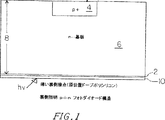
図1は、裏面入射のp−i−nフォトダイオード構造で用いられる本発明による組み合わせを概略的に図示する。光子は、光子透過性の電気伝導性裏面層2からデバイスに入る。この層は、バイアス電圧がこの層と、表面のp+インプラント領域4との間に掛けることができるように、電気接点としても働く。n――型シリコン基板6は通常、約250ないし1000μm(即ち1mm)の間の厚さ8を有する、ウェハ製造業者の供給するウェハである。基板厚さは4又は5mmまで厚くてもよい。基板厚さは電荷キャリアを空乏化させるのに必要な裏面電圧によって制限される。空乏化電圧は基板の厚さの二乗で増加する。このように、300μmの厚さに対して空乏化電圧が約30Vである場合、1mm厚さの基板に対して空乏化電圧は270Vとなり、2mm厚さの基板に対して空乏化電圧は1KVとなり、4mm厚さの基板に対して空乏化電圧は4KVとなる。アプリケーション及び検出装置の特性にもよるが、本発明による組み合わせは、基板厚さが使用できる範囲において使用される。普通、6インチのウェハは厚さ625μmで使用される。小径のウェハは普通、厚さも薄くなり、例えば550μm又は300μmである。大径のウェハの厚さは例えば750μmとなる。対照的に、フォトダイオード内のp+インプラント領域の厚さは、大抵の場合ただの約1μm(図1は縮尺通りには書いていない)である。随意的に、反射防止層10を裏面ウィンドウの上に蒸着してもよい。その厚さと構成は反射防止コーティングに関する周知の法則により求められる。本発明によるデバイスで良好に作動する材料の一つはインジウム錫酸化物(ITO)である。
【0012】
裏面層は電気伝導性があるので、これに対し、表面回路に関して正電圧を掛けると、中間にある電荷キャリアの基板を完全に空乏化することができる。こうすると暗電流を現実的レベルに制限でき、入射する光子によって作り出される電荷を暗電流越しに検出することができる。更に、電圧が掛けられることにより、光子の吸収によって作り出される電荷が基板の厚みを横切る際の広がりが制限される。そのため、電圧を掛けると、光子の吸収により作り出される以外の電荷キャリヤの基板を空乏化できるだけでなく、解像能を改善することもできる。
【0013】
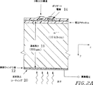
図2Aは、裏面入射の電荷結合素子(CCD)に用いられる本発明による組み合わせを概略的に示す。光子は、光子透過性の電気伝導裏面層12からデバイスの中に入る。この層は、バイアス電圧がこの層と、表面のゲート回路14との間に掛けることができるように、電気接点としても働く。n――型シリコン基板16は通常、約250ないし1000μm(即ち1mm)の間の厚さ18を有する、ウェハ製造業者の供給するウェハである。基板厚さは4又は5mmまで厚くてもよい。随意的に、反射防止層20を裏面ウィンドウの上に蒸着してもよい(縮尺通りに表示していない)。その厚さ及び構成は反射防止コーティングに関する周知の法則により求められる。本発明によるデバイスで良好に作動する材料の一つはインジウム錫酸化物(ITO)である。
【0014】
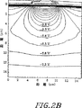
図2Bは、図2Aに示すような、高抵抗率シリコン基板上の一つのCCDのピクセルの2次元シミュレーションを示す。等電位線を0.5ボルト間隔で示している。集電ゲートには−5Vのバイアスが掛けられており、バリアフェーズは5Vにある。
【0015】
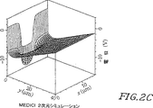
図2Cは、3層15μmピクセルに関する2次元電位分布のシミュレーションを示す。この図は、2次元ではなく3次元である点を除き、基本的には図2に示すのと同じデータを示す。1.5x1012cm-2のチャネルインプラントが使われている。基板のドーピングは(約7000Ω−cmの抵抗率に対応し)6x1011cm-3と想定されている。5μm幅の集電電極は−5Vに保持され、バリアフェーズは5Vであった。裏面バイアス電圧は、裏面電気接点まで伸びるドリフトフィールドを生成している(図2Cのy寸法)。
【0016】
裏面層にバイアス電圧を掛けることは本発明による光子検出エレメントの作動のキーである。裏面電圧は感光容積を完全に電荷空乏化し、電荷の拡がりを制限し、オンチップトランジスタ特性を改善する。(後に引用するIEDMペーパーの図2を参照)。しかしながら、この電圧は電界に対応する降伏電圧よりかなり低くなければならず、シリコンの場合室温で約2x10⁵V/cmである(S.M.Sze、半導体デバイスの物理学、第2版、ジョンウイリィ・アンド・サン、103頁、1981年)。極端に少数の電荷キャリヤ(N)を有する高抵抗率基板は、低い裏面電圧で完全な電荷空乏化が達成できるように、特別に製作される。
【0017】
十分な電圧を掛ければ基板は完全に電荷キャリヤの空乏化ができるので、基板の厚さは、従来の裏面入射CCDsの場合よりもかなり厚くできる。厚い基板には、機械的強度、長波長光子の吸収、製作経済性をはじめ幾つもの利点がある。
【0018】
本発明による組み合わせの基板の厚さ(図1の8,図2Aの18)は約100μmと約5mmの間にある。経済的製作経済性、機械的強度、電化空乏化の容易性、の3つの理由から、基板厚さの下限は約200μであるのが望ましい。経済的製作性のため、機械的強度のため、そして長波長光子及び短波長光子を検出するためには、更に、基板厚さの下限を約250μとするのが望ましい。厚さ10mmの基板が、その長い吸収長の故に、高エネルギーX線光子の検出に使用される。現実的範囲としては、基板の厚さは、対象の光子の吸収長の約2ないし3倍の間の厚さが用いられる。それ故、例えば、赤外部(IR)近くの光子を検出するには、基板厚さは約300μmのものが良好に機能する。
【0019】
本発明による電気伝導性光子透過性裏面層の厚さは、部分的には、検出器で感知される放射の形式の関数である。短波長光子に対しては、裏面層は非常に薄くなければならない。長波長光子に対しては、裏面層は厚くてもよい。裏面層の厚さに関する機能的な制限は、検出の対象である入射光子に対して透過性でなければならないということである。裏面層が漸進的に厚くされるにつれ、短波長光子に対しては不透過性となる。
【0020】
伝導性裏面層は、検出器の用途により、約10nmないし100μmの間の厚さとなるように作ることができる。100μmの裏面層の厚さは丁度シリコンバンドギャップの下にあり、約1000ないし1100nmの間の波長を有する光子に対してだけ透過性となる。厚さ10μmの裏面層は、約800ないし1100nmの間の波長を有する光子に対して透過性となる。現在の蒸着技術を用いれば、10μmのポリシリコン層は、蒸着に60時間を要する。さらに一般的には、本発明による光子検出器は、約10nmないし1μmの間の厚さを持った裏面層で作られる。厚さ1μmの裏面層は、約550ないし1100nmの間の波長を有する光子に対して透過性となり、この中には赤及び赤外部が含まれる。10ないし100nmの裏面層は、長波長光子のみならず青の光子にも透過性となり、この厚さ領域の裏面層を有する幾つかのデバイスが作られている。裏面層厚さの最も有用な範囲は約10ないし50nmの間にあり、それはこの範囲が短波長光子と長波長光子両方に透過性となり、且つ蒸着段階に必要とされる時間が、もっと厚い裏面層より短いからである。
【0021】
シリコン内の光子吸収長は温度に依存し、温度が下がるほど吸収長が増える。基板厚さが、検出される光子の吸収長の2又は3倍以上であれば、電荷空乏化に過剰な裏面電圧が必要となる。完全な電荷空乏化に必要な裏面電圧は基板厚さの二乗で増加する。更に、基板厚さが光子吸収に必要な以上に厚ければ、解像に幾らかロスが生じる。
【0022】
光電検出器では、暗電流を低く維持するのが重要である。暗電流を低く保つ一つの方法は、暗電流を増加させない原位置ドープCVD裏面層を使用することである。
【0023】
ポリシリコン層は原位置ドープされ電気伝導性となる。ドーピングは、電気伝導性を増す、ポリシリコンにとっての追加の要素である。ウィンドウ層は、シリコン内に小さな吸収深さを有する短波長光に対して透過性とするため、光学的に薄い。
【0024】
ポリシリコンをドープするにはいろいろな方法がある。CVDを用いれば、裏薄上にn+層を確保でき、これは良好な短波長光吸収に必要である。ドーピングのもう一つの方法はドーパントのイオン注入であるが、現存の注入器では、このように薄い(100A)層に容易に注入することはできない。更に、イオン注入は暗電流を増加させることになりかねない熱サイクルを必要とする。更に又他のドーピング技法は熱拡散法を用いたドーピングであるが、今述べたのと同じ問題を有する。
【0025】
薄い裏面層をドーピングするのに使えるもう一つの方法は、分子線エキタピシ法であるが、非常に費用がかかる。費用が問題でない場合、この方法で行うのは幾らか利点がある。
【0026】
本発明による組み合わせは、シリコンウェハを薄くする必要がないので、特別に良好な長波長応答性を有している。活性容積(シリコンウェハの厚さ)は通常のCCDs又は他のセンサーよりも遙かに厚いので、赤外部領域にあるような長波長光子はシリコンの活性容量内で吸収されそれを通過させる代わりに電荷キャリアを生成する。
【0027】
薄い裏面ポリシリコン層は、基板を空乏化するためにバイアス電圧を掛けることを考慮した透過性電気接点としても働く。シリコンは屈折率(3.7)が高いので、層の反射率はかなり高い。例えば、反射率は長波長では33%であり、短波長ではもっと大きい。裏面ウィンドウ層の反射率を下げる伝導コーティングを施せば、本発明による組み合わせの量子効率が上がる。
【0028】
透過性低抵抗率裏面層とシリコンウェハの本発明による組み合わせは、更に反射防止層(図1の10、図2の20)と組み合わされる。反射防止層は、電気伝導性で透過性の、例えば、インジウム錫酸化物(ITO)であるのが望ましい。原位置ドープされたポリシリコンをITOでコーティングすれば、反射ロスは低くなり、その結果量子効率はよくなる。伝導性外層を使えば、更に直列抵抗が減り、低ノイズデバイスが作れる。裏面層とシリコンウェハの組み合わせにITOコーティングを施せば、ほぼ2の因数の暗電流の低減が観察された。
【0029】
ITO層は反応スパッタリングによって蒸着された。イオン化したアルゴン原子がバイアスを掛けられたITOターゲットに引きつけられて、ITO分子を昇華させた。分子は基板の裏面層上に、それを直接ITOターゲットから直接対抗する側に配置することにより蒸着される。
【0030】
本発明による組み合わせの主要な利点は、裏面ウィンドウ層が、紫外部から赤外部までX線を含め、光子の全スペクトルに対し透過性であり、光子が活性シリコン容積6に入って電荷キャリアを生成できることである。比較的厚いシリコンウェハに裏面ウィンドウを施すのには、幾つかの利点がある。
・厚いデバイスは薄いデバイスほどにはひずみの影響を受けにくい。
・裏面層に電圧を掛け、裏面接点付近に実質的に零電界領域のない、完全に荷電空乏化されたデバイスを作り出すことができる(このような零電界領域は望ましくない重大な電荷拡散を起こす)。
・薄いデバイスで問題となる、赤の縞が取り除かれる。
・本発明による組み合わせを使う検出デバイスは、薄くする必要無しに対応する良好な青の応答を備えて裏面入射することができる。
・活性容積は長波長光子に対し透過性ではない。
【0031】
活性シリコン容積の厚さは、長波長光子を吸収しそれにより検出するように選定することができる一方、その同じ厚さは、例えば青及び紫外部領域にある短波長光子により作り出される荷電キャリアのロスに結びつきかねない。短波長光子の検出を助けるために、導電性裏面ウィンドウ層(又は随意的ITOコーティング)とフォトダイオードのp+領域との間に電圧が掛けられる。CCD又は活性ピクセルセンサーの場合、(随意的にITO及び/又は他の反射防止コーティングを有する)導電性裏面ウィンドウ層とポリシリコンゲートとの間に電圧が掛けられる。ゲート電極は埋設チャネル間を横切る電圧低下を引き起こし、埋設チャネル接合部の電圧と裏面電圧との間の差がキャリアがドリフトする電界を決める(S.ホランド他「天文学及び天体物理学で使用するための裏面入射の完全空乏化CCD画像センサーの開発」電荷結合素子及び進化した画像センサーに関するIEEE研究会、ベルギー、ブルージェ、1997年6月5−7日)。
【0032】
ポリシリコン層は、暗電流を著しく増加させることなく高抵抗率基板を完全に空乏化するに必要なバイアス電圧に耐えうる。バイアス電圧は高抵抗率n型基板内の少数の可動電子を取り除いて、光子によって生成された電荷が、空間解像のロスを引き起こすことになる、再結合又は拡散をする前にこれを集めるのに必要な電界となる、イオン化されたドナー原子を後に残す。
【0033】
電圧バイアスをシリコンフォトデバイスの裏面と表面との間に掛ける際に生じうる問題の一つは、ピクセルとCCDsのためのチャネルストップインプラントのような絶縁構造との間の電圧降伏が起こりうることである。CCDコラムは他からチャネルストップインプラントにより絶縁されているが、このインプラントはイオンインプラントであり、容積の中よりもCCDの表面により大きなドーパント不純物の集中を引き起こす。その効果は隣接するコラム間に電位バリアを作ることである。
【0034】
もしこれらの領域がCCD内で電気的に浮動していれば、高い電界がCCDチャネルとチャネルストップインプラントとの間に形成され、降伏につながりかねない。CCDチャネルは空乏化されているので、チャネル内の電位は通常、掛けられたゲート電圧より5−10V以上低い。チャネルストップインプラントは、n型基板に対しては正である、掛けられた基板バイアスの幾らか分浮上する傾向にある。
【0035】
裏面ウィンドウと光子検出デバイスの表面との間に電圧を掛けると、完全に電荷空乏化された光子感知容積が作り出せる。これは又、光子により生成された電荷キャリアが検出器の表面に向けて動くので、電荷の拡がり、即ちブルームを制限することにより空間解像度を改善する。
【0036】
降伏を避けるために、インプラントされていないシリコンのわずかなギャップがチャネルとチャネルストップインプラントとの間に残される。この領域は軽くドープされるので、電界は低くなっており降伏が避けられる。
【0037】
現在の実施例の多く(例えば、CCDs、フォトダイオード、活性ピクセルセンサー)はn型基板を使用しているが、この技法は又、p型シリコン上に組み立てられる放射検出器にも適用されてきた。その場合、絶縁インプラントはシリコン上の2酸化シリコン層内の固定電荷を補償する必要がある。常に正に充電されている固定電荷が存在しない場合、隣接するエレメントを短絡することのできる電子の逆転層を生じることになる。
【0038】
バイアス電圧VBは、光子感知シリコン容量の抵抗を始めとする幾つかの因子に基づいて選定される。
【0039】
利用できる最小バイアス電圧VB-MINは、空乏化電圧に等しい。しかし実用的見地から、普通は空乏化電圧よりも幾らか高い電圧VBを用いる。我々は経験から、VB=VB-MIN+X%(VB-MIN)を用いたが、ここにX=N(空乏化領域内のcm3当たりのドーパント原子の数)の変数である。シリコン基板中の抵抗が約10−12kΩ−cmである場合、通常VB=35Vが使用される。最大VBは、1次電荷キャリアの衝突イオン化による2次キャリアの存在により制限されるが、この現象はノイズの増加と電圧降伏により観察される。
【0040】
空乏化電圧VDは、
VD=(0.5qN(xD)2)/εS
で与えられ、ここに、Nは空乏化領域内のcm3当たりのドーパント原子の数、xDは空乏化領域の長さ、qは電子の電荷(1.602 10-19C)、εSはシリコンの誘電率(1.0 10-12F/cm)である。Nは抵抗率と、
ρ=(qμN)-1
の関係にあり、ここに、ρは抵抗率、μはキャリア移動度である(軽くドープされた材料に関しては、電子移動度は正孔移動度の3倍であることに留意のこと。このため、同一抵抗率に対して、n型シリコンの場合のNは、p型シリコンと比較して3倍少ない)。
【0041】
空乏化電圧はxDの二乗に比例するので、空乏化電圧を妥当な値に保つためにはNが小さくなければならない。xDが大きければ良好なIR近傍応答が期待でき、更にNが小さければ、良好なIR近傍応答及び妥当な基板電圧下での裏面入射の可能性という、両方の世界でベストの結果が得られる。
【0042】
表Iは種々の高抵抗率CCDsについて、ρ及びNを比較したものである(正孔移動度を約500cm2/V−sec、電子移動度を1500cm2/V−secと仮定している)。
100μmと1000μmの間の基板を妥当な電圧で空乏化するには極端に低いNが必要となる。上の表が示すように、本発明は十分に低いNを持って組み立てられている。他の基板、例えば、ウェスチングハウスの研究者により開発された、低いNを持つ基板は、通常のデバイスに使用できるよりも遙かに高い、極端に高い暗電流を呈している。一般的には、他が同じであれば、Nが低いほど、本発明によるデバイスの性能は良い(D.M.マッカム他「エリアアレイX線センサー」焦点面技術における進化、SPIE会報、118−128,198頁)。
【0044】
低いNを使う利点は基板が比較的低い電圧(約20−25V)で空乏化できることにある。これによって降伏の問題は起こりにくくなり、CCDピクセルと出力増幅器の一方若しくは両方についての問題に関わる懸念が少なくなる。両方の懸念共に、極端に低いNに対する強固に2次元的な特性によるものである。トランジスタ及びCCDの特性は、電圧が降伏電圧以下にとどまる限り、裏面電圧の増加と共に改善される。電界及び裏面電圧の強い2次元特性は2次元電界を幾らか平坦にする。裏面電圧のCCD出力トランジスタ特性に与える影響は、S.ホランド他の「高抵抗率シリコン上に作られた、200x200CCD画像センサー」(国際電子デバイス会議(IEDM)技術ダイジェスト、911−14頁、1996年、カリフォルニア州サンフランシスコ)で議論されている。
【0045】
十分に低いNの高抵抗率シリコンを得るために、ドイツのバッカーケムトロニック社が注文仕様を準備している。このドイツの会社に渡す仕様を以下の例に示す。WフォンアモンとHヘルツァは、低N高抵抗率基板の製作について、彼らの論文「検出器に使うための高抵抗率シリコンの製造と入手性」(物理研究における核計測及び方法、A226、94−102頁、1984年)で論議している。
【0046】
出力トランジスタにとって、パンチスルーが懸念事項であり、CCDピクセルにとっては、ポテンシャルウェルを形成し電荷を蓄える能力が関心事である。1つのピクセルから他のピクセルへとスピルオーバーする電荷を持ったチャネルに沿うピクセルの間の絶縁は劣っていても良い(チャネルストップインプラントの影響を受けず、これがチャネルを互いに絶縁する)。
【0047】
反射防止コーティングを用いれば反射ロスは低減できる。2酸化シリコン(屈折率1.45の絶縁材)及びインジウム錫酸化物(透過性で屈折率1.8−2.2の導体)は共に成功裏に使用されてきた。使用できるものは他にもたくさんある。
【0048】
陽電子放射断層撮影法(PET)で用いられるフォトダイオードに関しては、ITO厚さは、シンチレーションしている水晶が特定の波長の光子を放射する所望の波長に調整された(S.ホランド他「低ノイズ、裏面入射シリコンフォトダイオードアレイの開発」核科学に関するIEEE会報、44(3)、443−7,1997年6月)。約4分の1波長厚のITOが蒸着された。もう一つのアプローチは反射防止特性のための2つのコーティング、即ち、ITOの下層及び2酸化シリコンの上層、を用いることである。反射防止コーティングの技術は良く開発されており、本発明による組み合わせの裏面ウィンドウに適用できる。そのような材料と議論の2つのソースはブルックとM.D.ネルソンの論文「電荷結合素子のための安定した紫外部反射防止コーティング」(SPIE1900、228−240、1993年)及びM.レッサーの論文「シリコン電荷結合素子のための反射防止コーティング」(光学技術、26(9)、911−915、1987年)である。
【0049】
透過性の伝導性酸化物(TCOs)と称されるクラスの材料で作られたフィルムはITOの代替材を提供し、同様な特性を有している。一般的に、低い屈折率を有するフィルムは何れも反射防止コーティングとして使用できるが、高抵抗率の層は、ある環境下、例えば非常に鮮やかな画像に対しては、望ましくない程に不均一な裏面電圧を生ずる結果となる。反射防止コーティングとしてのこの他の候補材には、酸化ハフニウム、酸化鉛、酸化アルミニウム、窒化シリコン、フッ化マグネシウムが挙げられる。
【0050】
インジウム錫酸化物は以下の多くの利点を有している。
【0051】
1)導電性であり、薄い裏面層の抵抗を低減する(フォトダイオードの場合ノイズを配慮すると、そしてCCD用に裏面上に等電位を作り出すためには重要である)。
【0052】
2)屈折率は空気/ITO/シリコンのインタフェースに適している(中間フィルムが空気とシリコンの幾何学的中間である屈折率を有する場合、4分の1波長板に対応する波長で理論的にはゼロの屈折率となる)。これは先に引用したIEEE核科学論文に詳しく議論されている。
【0053】
3)室温で蒸着され、漏洩電流を低下させない。
【0054】
4)導電性なので、物理的裏面接点が容易に作れる。
【0055】
MgFのような絶縁層は薄いポリシリコン裏面層と互換性がある。しかし、絶縁材を反射防止層として使う場合、裏面接点を作るために絶縁材の一部を取り除くか、或いは電圧を表面に掛けて裏面はフロートさせておくかしなければならない。
【0056】
高抵抗率シリコン基板を光子感知容積として使って作られたCCDは本発明の一つの態様である。このような高抵抗率シリコンで作られたCCDが、裏面に電気伝導性の層をつけて、或いはそれ無しで、有効に作動するのは驚くべきことである。高抵抗率容量は電位を強く2次元化し、多くの人は、そのような高抵抗率材中にはポテンシャルウェルは機能的に形成されないであろうと思っている。
【0057】
ピクセルは本発明によるデバイスでは15x15μm2と小さく作られている。高抵抗率材上にそのように小さなピクセルを作ることができるとは思われていなかった。低抵抗率シリコン上の商業ベースのデバイスのピクセルのサイズは27x27μm2か18x24μm2かの何れかである。
【0058】
裏面層はリンで、約0.0001ないし10原子パーセントドーピングの間にドーピングされる。リンで、約0.001ないし3原子パーセントの間にドーピングされるのがより好ましい。リンで、約0.1ないし3原子パーセントの間にドーピングされるのが最も好ましい。作動モデルは約1ないし1.5原子パーセントのリンのドーピングを使い、アニーリングなしで作られた。詳細は先に引用した核科学に関するIEEE会報に述べられている。
【0059】
表面ピニング。CCDの暗電流はバルク成分と表面成分の両方を持っている。リンでドーピングされたポリシリコン層から効果的にゲッタリングすれば、表面成分を暗電流の主要ソースとして残しながら、バルク成分を大きく低減することができる。
【0060】
表面電流を低減する技術には、表面のインタフェース状態をチャネルストップインプラントから供給されるキャリアで満たすことが含まれる。デバイスの前にあるポリシリコンゲート電極には、キャリアの逆転層が作り出されて表面状態を満たすように、バイアスが掛けられている。一旦満たされると、この状態はもはや暗電流には寄与しない。表面に可動キャリアが集中し電位を釘付けにするが、これを表面ピニングと呼ぶ。この技法はチャネルストップインプラントにバイアスが掛けられていることを必要とする(通常は接地電位で)。
【0061】
完全に空乏化されたCCDに対しては、裏面ウィンドウに掛けられたバイアスとCCDそれ自身の外のチャネルストップ接点との間にオーミックパスがあってもよく、その結果は裏面とチャネルストップの間に大電流が流れることになる。適切なジオメトリ(即ち、前面上のn+接点がp+で取り巻かれていなければならないか、又はCCDピクセルが両側になければならない)を有する単純なダイオード構造を使えばチャネルストップ電流は低減される。このジオメトリ設計は近くのp−n接合部を経由してチャネルストップに逆バイアスを掛ける。
【0062】
上記のCCDジオメトリと組み合わせて使用した場合、表面電流を著しく低減できる技術が他にもある。低温での長い放射時間は、表面状態でキャリアをトラップする。先ずキャリアに、チャネルストップが接続され、全てのCCDゲートが表面キャリアタイプを逆転するに十分な電位に保持されている状態下で、表面状態を満たさせる。次に、チャネルストップ接点は浮動化され、長放射時間定数がCCDの作動の間、表面電流を低く維持する。
【0063】
裏面上の正しい方向を指すように電界を保つためのUV充電のような信頼性のない技法は、本発明の裏面層に掛けられる電圧がこの問題を取り除くので、本発明を用いれば回避できる(「高抵抗率シリコン上に作られた、200x200CCD画像センサー」国際電子デバイス会議(IEDM)技術ダイジェスト、911−14頁、1996年、カリフォルニア州サンフランシスコ)。
【0064】
問題は自然の酸化物が自然にシリコン上に形成されることである。シリコン上の酸化物は常に、インタフェースに一定の正の電荷を持っている。通常使用されているp型シリコンでは、この正の電荷が裏面に小さな空乏層を形成する。短波長光子に対しては、生成された電子にこの一定電荷が裏面に向けて付加される。解決策は、この一定の正電荷にうち勝つために電子の表面層を作り出す裏面のUV充電である。もう一つのの技法は、薄い透過性ゲートの仕事関数が正電荷にうち勝つフラッシュゲートである。
【0065】
この問題を解決するためのもう一つの試みでは、RCAの研究者が、正電荷が働くn型シリコン上の従来型低抵抗率CCDで、ホールをポテンシャルウェルに向けて反射させている。本発明を使用すれば、裏面電圧を掛けるとこの問題は解消する。CCDがp型基板で作られている場合でも、本発明を使用すれば、電荷の基板を空乏化するだけの十分大きな裏面電圧は、正電荷を償う以上となる。
【0066】
本発明による放射感知デバイスに関しては幾つかの重要なパラメータがある。
・裏面層は約0.0001ないし10原子パーセントドーピングの間に、リンでドーピングされる。約0.001ないし3原子パーセントの間に、リンでドーピングされるのがより望ましい。約0.1ないし3原子パーセントの間に、リンでドーピングされるのが最も望ましい。作動モデルは、約1原子パーセントのリンのドーピングを使い、アニーリングなしで作り上げられた。
・n型基板に関しては、光子感知容積に対して用いられる基板の抵抗率は、約100Ω−cmと約20KΩ−cmの間にあってもよい。約6KΩ−cmと約12KΩ−cmの間にあるのがより望ましい。
・p型基板に関しては、光子感知容積に対して用いられるシリコン基板の抵抗率は、約100KΩ−cmと約20KΩ−cmの間にあってもよい。約6KΩ−cmと15KΩ−cmの間にあるのがより望ましい。
・本発明による電気伝導性裏面層と光子感知シリコン容積の表面上の導電領域との間に掛けられるバイアス電圧は、上端がシリコン容積を横切る電圧降伏により、下端がバイアスにより生成されるキャリア速度により制限される。シリコン容積を横切るキャリア速度は、熱拡散による半径方向のキャリアの動きにうち勝つだけ十分に大きくなければならない。
・(光子感知容積に用いられるシリコン基板の)抵抗率が低くなるにつれ、完全空乏化に必要な電圧は減少する。感光容積シリコンの抵抗が低くなりすぎると、バイアス電圧が降伏を引き起こすか、或いは状態が空乏化する前に過度のノイズを生じる。
・(光子感知容積に用いられるシリコン基板の)抵抗率が高くなるにつれ、CCDゲート下のポテンシャルウェルのジオメトリはより2次元的となり、トランジスタ特性は劣化する。この現象は、シリコン基板で使用できる最高抵抗率を制限する。2次元効果は部分的には、裏面電圧を上げることにより補償できる。裏面電圧が空乏化電圧を超えると2つの項が電界を記述する(先に言及した、1997年IEEEベルギー研究会報告書の式2を参照)。Nが非常に小さい場合には、Vappl/Ydが支配的で、Nの値は重要ではない。数多くの2次元シミュレーションが、高抵抗率CCDの全ウェル容量を低抵抗率CCD(約20Ωcm)と比較するために行われた。驚くべきことに、先のレポートとは対照的に、2つの抵抗率状態の間で、全ウェル容量には差が見られなかった。ウェルの平坦化がおそらく裏面電圧によって補償されたのであろう。
・本発明による電気伝導性裏面層の厚さは部分的には、検出器によって感知される放射の形式の関数である。短波長光子に対しては、裏面層は非常に薄くなければならない。長波長光子に対しては裏面層は厚くてもよい。裏面層の厚さに関する機能的制限は、それが検出対象の入射光子に対して透過性でなければならないということである。裏面層が漸進的に厚くされるにつれ、短波長光子に対しては不透過性となる。裏面層は、検出器の用途により、約10nmと約1000μmとの間の厚さを有するように成功裏に作られてきた。より好ましくは、漏洩電流を最小化するために裏面層を約10nmと約100μmの間にするのがよい。
【0067】
実施例1:裏面ウィンドウの製作
本発明による裏面ウィンドウは、ホスフィン(PH3)が存在する中で、高抵抗率シリコン基板上に、シラン(SiH4)の低圧化学蒸着(CVD)により蒸着される。この処理は低温、即ち約650℃で、極度にクリーンな環境下で行われ、不純物は10億分の1以下に保たれる。これは低温の工程なので、多結晶シリコン(ポリシリコン)層の蒸着は、高温の処理が全て完了した後、プロセスの終わり近くで行われる。以下のプロセスプロトコルはウィンドウを適用するための一つの順序を示す。バキュームチャンバーの側壁はチャンバー壁上に蒸着したポリシリコンで覆われている。使用されるガスの純度は99.999%である。シリコンウェハは、もし一般的に受け入れられているとすれば、必要なプロトコルによって予洗浄される。基板は、裏面ウィンドウが蒸着される前に、ゲッタリング処理に掛けられる。厚い、リンでドーピングされたポリシリコンがゲッタリングに用いられ、次に、裏面ウィンドウが蒸着される前にエッチングされる。ゲッタリングの工程は、S.ホランドが「高抵抗率シリコン上への検出器とトランジスタの製作」と題する1989年の物理研究における核計測及び方法、A275、537−541頁、で公にしている方法に従って行われる。このプロセスは実質的に金属汚染物を含まない基板を提供する。
【0068】
裏面層は約0.0001ないし約10原子パーセントドーピングの間にリンでドーピングされる。約0.001ないし約3原子パーセントの間にリンでドーピングされるのがより望ましい。約0.1ないし約3原子パーセントの間にリンでドーピングされるのが最も望ましい。作動モデルは約1原子パーセントのリンのドーピングを使って作られた。
【0069】
基本的に、薄い裏面ポリシリコンウィンドウの蒸着は以下の工程で行われる。
a.最終希釈HFエッチングとそれに続くDIリンスの追加による標準予拡散洗浄。
b.サームコレシピDPOLYを用いたウェハ裏面上のドーピングされたポリシリコンのLPCVD。
c.モニターウェハ上のポリシリコン厚さの計測。
【0070】
処理は温度約650℃、圧力400ミリトールで、SiH4中1%PH3のガスフローを使って行う。
【0071】
実施例2:低N基板の入手
所望の高抵抗率、低Nシリコンウェハを入手するため、幾つかの候補ウェハメーカーから入札が得られた。ここに記載する実験の大部分に使われたウェハは、ワッカーシルトロニック社、地区販売室(カリフォルニア州95117、サンジョゼ、#114、モールパーク通り4010、408/554−9728)からの注文生産品である。ウェハは以下の仕様に従って製作された。
1.型式:n型、リンドーピング、フロートゾーン不純物除去、無転移
2.結晶体方位:<100>
3.抵抗率:6000Ω−cm以上、好ましくは10,000Ω−cm近く
4.小数キャリア寿命:1ミリ秒以上
5.直径:100mm
6.呼び厚:300μm
7.平坦度:SEMI標準による
8.エッジ:エッジには、取り扱いの間にウェハの破壊につながる恐れのあるエッジ亀裂が生じるのを最小化するために、丸みを付けること。
9.ウェハ仕上げ:片側研磨、反対側は損傷無きこと、即ち、裏面には故意の損傷又はゲッタリングなし。
10.厚み許容差:+/−15μm max.
11.テーパ:<5μm max.
12.曲がり:<30μm max.
13.数量:500ウェハ
【0072】
実施例3:電気伝導性、光子透過性の裏面層を有するフォトダイオードの製作
以下のプロセスフローは、裏面に電気伝導性、光子透過性ポリシリコン層を有する裏面入射フォトダイオードをn型基板上に製作するために使われた。更新されたプロトコルが、カリフォルニア州バークレイのローレンスバークレイ国立研究所、電話510/486−4000の発明者より入手可能である。
【0073】
開始材料:抵抗率4kΩ−cm以上、厚さ300μm、<100>n型シリコン(ワッカーからの注文仕様品)の基板用シリコンウェハ。
(1)低温酸化物蒸着
a.標準予拡散洗浄
110℃で5分間ピラーニャ(WPS2)
DI水リンス(WPS2)
希釈HFエッチング(WPS2)
DI水リンス(WPS2)
40℃で5分間メガソニックRCA I洗浄(WPS2)
DI水リンス(WPS2)
希釈HFエッチング(WPS2)
DI水リンス(WPS1)
40℃で5分間メガソニックRCA II洗浄(WPS1)
DI水リンス(WPS1)
b.5000AのSiO2のLPCVD、サームコレシピUDLTOを使用し、425℃で、30分間の蒸着
c.モニターウェハ上の酸化物厚さ計測
(2)裏面酸化物除去
a.LP3にウェハを準備(HMDSアプリケーション)
b.OCG825フォトレジストをスピン(MTIレシピ#1)
c.ウェハを30分間120℃でハードベーク
d.ウェハを、裏面酸化物が完全に除去されるまで、6:1緩衝酸化物エッチング(BOE)でエッチング
e.ピラーニャでレジスト剥ぎ取り(WSP5)
(3)1μm原位置ドープポリシリコン蒸着
a.最終希釈HFエッチングとそれに続くDIリンスの追加による標準予拡散洗浄。
b.ウェハ裏面上のドーピングされたポリシリコンのLPCVD、サームコレシピDPOLYを用いた約6時間の蒸着
c.モニターウェハ上のポリシリコン厚さ計測
(4)1000A窒化物蒸着
a.予拡散洗浄、但し、ウェハがドーピングされたポリシリコンの蒸着に続いて直ぐに窒化物のチューブにローディングされた場合は不要
b.ウェハ裏面に1000Aの窒化シリコンのLPCVD、サームコレシピNITRIDEを使用し、47分間の蒸着
(5)表面窒化物/ポリ除去
a.技法cエッチャーオンキャンパスを用いて表面窒化物/ポリをプラズマエッチング。100W、280ミリトール、13sccmSF6、21sccmHe。
(6)表面LTO除去
a.BOEで表面LTOをエッチング
(7)4000Aフィールド酸化
a.標準予拡散洗浄
b.4000Aのフィールド酸化物を成長させるための蒸気酸化、サームコレシピWET4000A、チューブ2−1を使用し、900℃で4時間45分、酸化前にサームコレシピ1TCACLNを使用し炉チューブのTCA洗浄
c.モニターウェハ上の酸化物厚さを計測
(8)マスク1(p+インプラント)
a.LP3にウェハを準備(HMDSアプリケーション)
b.OCG825フォトレジストをスピン(MTIレシピ#1)
c.マスク1を使用して露出(0.6秒露出)
d.3:1DI水:OCG809で現像(WPS3)
e.検査
(9)酸化物エッチング
a.ウェハを30分間120℃でハードベーク
b.1000A熱酸化物テストウェハを用いて6:1緩衝酸化物エッチング(BOE)速度のエッチング速度を決定
c.BOEエッチング速度と計測厚さに基づき、必要なエッチング時間を算出。湿潤化に必要な全ての時間に加えて、この時間に20%を加え、ウェハをエッチング。
d.DI水リンスの後、大きなエッチング面上で疎水性表面挙動を検査。完全な酸化物除去を確認するため、残留酸化物厚さをナノ仕様で計測。
e.ピラーニャでレジストを剥ぎ取り(WPS5)
(10)ボロンのインプラント
a.B+、2 1015cm-2のドーズ、30keVのエネルギー、7度のチルト角
(11)1000A熱酸化/インプラントアニール
a.標準予拡散洗浄:
b.1000Aのフィールド酸化物を成長させるための蒸気酸化(900℃で37分)し、続いて2時間の窒化物アニール、サームコレシピW1000DET、チューブ2−1、酸化前にサームコレシピ1TCACLNを使用し炉チューブのTCA洗浄
c.モニターウェハ上の酸化物厚さを計測
(12)裏面の酸窒化物/窒化物の除去
a.LP3にウェハを準備(HMDSアプリケーション)
b.OCG825フォトレジストをスピン(MTIレシピ#1)
c.ウェハを30分間120℃でハードベーク
d.ウェハを、裏面酸化物を除去するため、6:1緩衝酸化物エッチング(BOE)で3分間エッチング
e.ピラーニャでレジストを剥ぎ取り(WPS5)
f.裏面窒化物をリン酸中にて190℃で除去
(13)裏面ポリシリコンの除去
a.LP3にウェハを準備(HMDSアプリケーション)
b.OCG825フォトレジストをスピン(MTIレシピ#1)
c.ウェハを30分間120℃でハードベーク
d.ウェハを、裏面ポリシリコン及び拡散n+層が除去されるまで、シリコンエッチングでエッチング。裏面ポリ蒸着からのモニターウェハを使用して適切なエッチング時間を定め、裏面ウェハ上で4点探針計測により除去を確認
(14)薄い裏面ポリシリコン蒸着
a.最終希釈HFエッチングとそれに続くDIリンスの追加による標準予拡散洗浄。
b.サームコレシピDPOLYを用い、ウェハ裏面上のドーピングされたポリシリコンのLPCVD、
c.モニターウェハ上のポリシリコン厚さ計測
(15)表面ポリシリコン除去
a.技法cエッチャーオンキャンパスを用いて表面ポリシリコンをプラズマエッチング。100W、280ミリトール、13sccmSF6、21sccmHe。酸化物に対するこのエッチングの比較的劣った感度によるオーバーエッチングの最小化。
b.ピラーニャでウェハを洗浄(WPS5)
(16)マスク2(接点マスク)
a.LP3にウェハを準備(HMDSアプリケーション)
b.OCG825フォトレジストをスピン(MTIレシピ#1)
c.マスク4を使用して露出(0.6秒露出)
d.3:1DI水:OCG809で現像(WPS3)
e.検査
(17)接点エッチング
a.ウェハを30分間120℃でハードベーク
b.低温酸化物モニターウェハを用いて6:1緩衝酸化物エッチング(BOE)速度のエッチング速度を決定
c.BOEエッチング速度と計測厚さに基づき、必要なエッチング時間を算出。湿潤化に必要な全ての時間に加えて、この時間に20%を加え、ウェハをエッチング。
d.DI水リンスの後、大きなエッチング面上で疎水性表面挙動を検査。完全な酸化物除去を確認するため、残留酸化物厚さをナノ仕様で計測。
e.ピラーニャでレジストを剥ぎ取り(WPS5)
(18)0.5μmアルミニウム蒸着
a.希釈HFバスのエッチング速度を決定
b.エッチング速度計測に基づき、60Aの酸化物を除去するためにエッチング
c.ウェハをMRC603にロード
d.6kW、15cm/秒、10ミリトールでアルミニウムをスパッタリング
(19)マスク5(融解マスク)
a.LP3にウェハを準備(HMDSアプリケーション)
b.OCG825フォトレジストをスピン(MTIレシピ#1)
c.マスク5を使用して露出(0.6秒露出)
d.3:1DI水:OCG809で現像(WPS3)
e.検査
(20)メタルエッチング
a.ウェハを30分間120℃でハードベーク
b.ウェハをアルミニウムエッチング液中にて30℃でエッチング
c.キャンパス技法cプラズマエッチャーでシリコン残留物を除去
d.PRS−2000でレジストを剥ぎ取り(WPS5)
(21)焼結
a.サームコレシピSINT400,チューブ1−2を使い、成形ガス中にて400℃で焼結
(22)裏面ITO蒸着/アニール
実施例5参照
【0074】
実施例4 CCD
以下のプロセスフローは、裏面に電気伝導性、光子透過性ポリシリコン層を有する裏面入射電荷結合素子をn型基板上に製作するために使われた。
【0075】
開始材料:抵抗率4kΩ−cm以上、厚さ300μm、<100>n型シリコン(ワッカーからの注文仕様品)の基板用シリコンウェハ。
(1)低温酸化物蒸着
a.標準予拡散洗浄
100℃で5分間ピラーニャ(WPS2)
DI水リンス(WPS2)
希釈HFエッチング(WPS2)
DI水リンス(WPS2)
40℃で5分間メガソニックRCA I洗浄(WPS2)
DI水リンス(WPS2)
希釈HFエッチング(WPS2)
DI水リンス(WPS1)
45℃で5分間メガソニックRCA II洗浄(WPS1)
DI水リンス(WPS1)
b.5000AのSiO2のLPCVD、サームコレシピUDLTOを使用し、425℃で、30分間の蒸着
c.モニターウェハ上の酸化物厚さ計測
(2)裏面酸化物除去
a.LP3にウェハを準備(HMDSアプリケーション)
b.OCG825フォトレジストをスピン(MTIレシピ#1)
c.ウェハを30分間120℃でハードベーク
d.OCG825フォトレジストで再コート(MTIレシピ#1)
e.ウェハを30分間120℃でハードベーク
f.ウェハを、裏面酸化物が完全に除去されるまで、6:1緩衝酸化物エッチング(BOE)でエッチング
g.ピラーニャでレジスト剥ぎ取り(WSP5)
(3)1μm原位置ドープポリシリコン蒸着
a.最終希釈HFエッチングとそれに続くDIリンスの追加による標準予拡散洗浄。
b.ウェハ裏面上のドーピングされたポリシリコンのLPCVD、サームコレシピDPOLYを用いた約6時間の蒸着
c.モニターウェハ上のポリシリコン厚さ計測
(4)1000A窒化物蒸着
a.予拡散洗浄、但し、ウェハがドーピングされたポリシリコンの蒸着に続いて直ぐに窒化物のチューブにローディングされた場合は不要
b.ウェハ裏面に1000Aの窒化シリコンのLPCVD、サームコレシピNITRIDEを使用し、47分間の蒸着
(5)表面窒化物/ポリ除去
a.技法cエッチャーオンキャンパスを用いて表面窒化物/ポリをプラズマエッチング。100W、280ミリトール、13sccmSF6、21sccmHe。
(6)表面LTO除去
a.BOEで表面LTOをエッチング
(7)500Aゲート酸化
a.標準予拡散洗浄
b.500Aのゲート酸化物を成長させるためTCAで酸化物を乾燥、サームコレシピD200GATW、チューブ2−2を使用し、900℃で3時間45分間、酸化前にサームコレシピ1TCACLNを使用し炉チューブのTCA洗浄
c.モニターウェハ上の酸化物厚さ計測
d.ウェハを速やかに窒化炉にロード
(8)500A窒化物蒸着
a.ウェハはゲート酸化炉から直接ロードされているので洗浄不要
b.500Aの窒化物蒸着、サームコレシピNITCCD、チューブ2−4を使って20.5分の蒸着
c.モニターウェハ上の窒化物厚さ計測
(9)マスク1(活性領域マスク)
a.LP3にウェハを準備(HMDSアプリケーション)
b.OCG825フォトレジストをスピン(MTIレシピ#1)
c.マスク4を使用して露出(0.6秒露出)
d.3:1DI水:OCG809で現像(WPS3)
e.検査
(10)窒化物エッチング
a.ウェハを30分間120℃でハードベーク
b.技法cプラズマエッチャーオンキャンパスを用いて窒化物エッチング。適切なエッチング時間を定め、その半分の時間エッチングし、ウェハを180度回転し、残り半分をエッチング(エッチングの均一性改善)
c.レジストを除去しないこと
(11)フィールドインプラント(リン)
a.1・1012cm-2のドーズ、30keVのエネルギー(照射範囲約0.15μm)、7度のチルト角(目標:酸化物厚さ0.5μmで250Vのフィールドスレッショルド電圧)
(12)レジスト/酸化物除去
a.ピラーニャでレジストの剥ぎ取り
b.プラズマエッチングの後6:1BHFで残余酸化物をエッチング
(13)4500Aフィールド酸化
a.標準予拡散洗浄:
b.4500Aのフィールド酸化物を成長させるための蒸気酸化、サームコレシピWET4500A、チューブ2−1を使用して450℃で5時間、酸化前にサームコレシピ1TCACLNを使用し炉チューブのTCA洗浄
c.モニターウェハ上の酸化物厚さを計測
(14)マスク2(チャネルマスク)
a.LP3にウェハを準備(HMDSアプリケーション)
b.OCG825フォトレジストをスピン(MTIレシピ#1)
c.マスク2を使用して露出(0.6秒露出)
d.3:1DI水:OCG809で現像(WPS3)
e.検査
(15)チャネルインプラント(ボロン)
a.1.0、1.5、及び2.0・1012cm-2のドーズ、150keVのエネルギー(照射範囲約0.4μm)、7度のチルト角
(16)レジスト除去
a.ピラーニャでレジストを除去
(17)ポリシリコン−1蒸着
a.標準予拡散洗浄。
b.ドーピングされていないポリシリコンのLPCVD、4500A。レシピPOLY4500、615/620/630℃で53.5分の蒸着、40sccmシラン前/後フロー、200ミリトール圧
c.モニターウェハ上のポリシリコン厚さ計測
(18)ポリシリコン−1インプラント(ボロン)
a.2.0・1015cm-2のドーズ、150keVのエネルギー(照射範囲約0.2μm)、7度のチルト角
(19)マスク3(ポリシリコン−1マスク)
a.LP3にウェハを準備(HMDSアプリケーション)
b.OCG825フォトレジストをスピン(MTIレシピ#1)
c.マスク3を使用して露出(0.6秒露出)
d.3:1DI水:OCG809で現像(WPS3)
e.検査
(20)ポリシリコン−1エッチング
a.ウェハを30分間120℃でハードベーク
b.ラム4プラズマエッチャーオンキャンパスを用いてポリをエッチング
c.酸素プラズマでレジストを剥ぎ取り、その後ピラーニャ洗浄
(21)裏面ポリシリコン−1の除去
a.LP3にウェハを準備(HMDSアプリケーション)
b.OCG825フォトレジストをスピン(MTIレシピ#1)
c.ウェハを30分間120℃でハードベーク
d.OCG825フォトレジストで再コート(MTIレシピ#1)
e.ウェハを30分間120℃でハードベーク
f.ポリをシリコンエッチング液中でエッチング
g.ピラーニャでレジストを剥ぎ取り
(22)ポリシリコン−1酸化
a.最終HFエッチングにより標準予拡散洗浄
b.1700Aのポリ間酸化物を成長させるためTCAで湿潤酸化、サームコレシピPOLY2K、チューブ2−1を使用し、950℃で30分、酸化前にサームコレシピ1TCACLNを使用し炉チューブのTCA洗浄
c.キャンパスnanoduvを使い、モニターウェハ上の酸化物厚さ計測
(23)ポリシリコン−2蒸着
a.ウェハが酸化チューブより直接ロードされている場合は洗浄不要
b.ドーピングされていないポリシリコンのLPCVD、4500A。レシピPOLY4500、615/620/630℃で53.5分の蒸着、40sccmシラン前/後フロー、200ミリトール圧
c.モニターウェハ上のポリシリコン厚さ計測
(24)ポリシリコン−2インプラント(ボロン)
a.2.0・1015cm-2のドーズ、80keVのエネルギー(照射範囲約0.2μm)、7度のチルト角
(25)マスク4(ポリシリコン−2マスク)
a.LP3にウェハを準備(HMDSアプリケーション)
b.OCG825フォトレジストをスピン(MTIレシピ#1)
c.マスク4を使用して露出(0.6秒露出)
d.3:1DI水:OCG809で現像(WPS3)
e.検査
(26)ポリシリコン−2エッチング
a.ウェハを30分間120℃でハードベーク
b.ラム4プラズマエッチャーオンキャンパスを用いてポリをエッチング
c.酸素プラズマでレジストを剥ぎ取り、その後ピラーニャ洗浄
(27)裏面ポリシリコン−2の除去
a.LP3にウェハを準備(HMDSアプリケーション)
b.OCG825フォトレジストをスピン(MTIレシピ#1)
c.ウェハを30分間120℃でハードベーク
d.OCG825フォトレジストで再コート(MTIレシピ#1)
e.ウェハを30分間120℃でハードベーク
f.ポリをシリコンエッチング液中でエッチング
g.ピラーニャでレジストを剥ぎ取り
(28)ポリシリコン−2酸化
a.最終HFエッチングにより標準予拡散洗浄
b.1700Aのポリ間酸化物を成長させるためTCAで湿潤酸化、サームコレシピPOLY2K、チューブ2−1を使用し、950℃で30分、酸化前にサームコレシピ1TCACLNを使用し炉チューブのTCA洗浄
c.キャンパスnanoduvを使い、モニターウェハ上の酸化物厚さ計測
(29)ポリシリコン−3蒸着
a.ウェハが酸化チューブより直接ロードされている場合は洗浄不要
b.ドーピングされていないポリシリコンのLPCVD、4500A。レシピPOLY4500、615/620/630℃で53.5分の蒸着、40sccmシラン前/後フロー、200ミリトール圧
c.モニターウェハ上のポリシリコン厚さ計測
(30)ポリシリコン−3インプラント(ボロン)
a.2.0・1015cm-2のドーズ、80keVのエネルギー(照射範囲約0.2μm)、7度のチルト角
(31)マスク5(ポリシリコン−3マスク)
a.LP3にウェハを準備(HMDSアプリケーション)
b.OCG825フォトレジストをスピン(MTIレシピ#1)
c.マスク5を使用して露出(0.6秒露出)
d.3:1DI水:OCG809で現像(WPS3)
e.検査
(32)ポリシリコン−3エッチング
a.ウェハを30分間120℃でハードベーク
b.ラム4プラズマエッチャーオンキャンパスを用いてポリをエッチング
c.酸素プラズマでレジストを剥ぎ取り、その後ピラーニャ洗浄
(33)裏面ポリシリコン−3の除去
a.LP3にウェハを準備(HMDSアプリケーション)
b.OCG825フォトレジストをスピン(MTIレシピ#1)
c.ウェハを30分間120℃でハードベーク
d.OCG825フォトレジストで再コート(MTIレシピ#1)
e.ウェハを30分間120℃でハードベーク
f.ポリをシリコンエッチング液中でエッチング
g.ピラーニャでレジストを剥ぎ取り
(34)ポリシリコン−3酸化
a.最終HFエッチングにより標準予拡散洗浄
b.1700Aのポリ間酸化物を成長させるためTCAで湿潤酸化、サームコレシピPOLY1K、チューブ2−1を使用し、900℃で30分、酸化前にサームコレシピ1TCACLNを使用し炉チューブのTCA洗浄
c.モニターウェハ上の酸化物厚さ計測
(35)マスク6(基板接点マスク)
a.LP3にウェハを準備(HMDSアプリケーション)
b.OCG825フォトレジストをスピン(MTIレシピ#1)
c.マスク6を使用して露出(0.6秒露出)
d.3:1DI水:OCG809で現像(WPS3)
e.検査
(36)酸化物エッチング
a.ウェハを30分間120℃でハードベーク
b.1000A熱酸化テストウェハを用いて6:1緩衝酸化物エッチング(BOE)速度のエッチング速度を決定
c.BOEエッチング速度と計測厚さに基づき、必要なエッチング時間を算出。湿潤化に必要な全ての時間に加えて、この時間に20%を加え、ウェハをエッチング。
d.DI水リンスの後、大きなエッチング面上で疎水性表面挙動を検査。完全な酸化物除去を確認するため、残留酸化物厚さをナノ仕様で計測。
e.ピラーニャでレジストを剥ぎ取り(WPS5)
(37)マスク7(基板接点インプラント)
a.LP3にウェハを準備(HMDSアプリケーション)
b.OCG825フォトレジストをスピン(MTIレシピ#1)
c.マスク7を使用して露出(0.6秒露出)
d.3:1DI水:OCG809で現像(WPS3)
e.検査
(38)基板接点インプラント
a.リン、P+、2.0・1015cm-2のドーズ、100keVのエネルギー、7度のチルト角、基板加熱を制限するためハイブリッドモードに植え込み
b.酸素プラズマでレジストを剥ぎ取り、続いてピラーニャ洗浄
(39)マスク8(浮動電極、ソース/ドレーンインプラント)
a.LP3にウェハを準備(HMDSアプリケーション)
b.OCG825フォトレジストをスピン(MTIレシピ#1)
c.マスク8を使用して露出(0.6秒露出)
d.3:1DI水:OCG809で現像(WPS3)
e.検査
(40)窒化物エッチング
a.技法cエッチャーオンキャンパスを使用して窒化物をプラズマエッチング
b.レジストを剥がさないこと
(41)浮動電極、ソース/ドレーンインプラント
a.B+、2・1015cm-2のドーズ、50keVのエネルギー、7度のチルト角、基板加熱を制限するためハイブリッドモードに植え込み
b.酸素プラズマでレジストを剥ぎ取り、続いてピラーニャ洗浄
(42)5000A酸化物蒸着(LTO/BPSG)
a.標準予拡散洗浄
b.SiO2の500AのLPCVD、サームコレシピUDLTOを使用して425℃で30分の蒸着
c.モニターウェハ上の酸化物厚さ計測
(43)高温形成ガスアニール
a.標準予拡散洗浄
b.1時間、サームコレシピFGANNEAL、チューブ1−1を使用し、形成ガス中で950℃アニール、酸化前にサームコレシピ1TCACLNを使用し炉チューブのTCA洗浄
c.モニターウェハ上の酸化物厚さ計測
(44)裏面酸窒化物/窒化物の除去
a.LP3にウェハを準備(HMDSアプリケーション)
b.OCG825フォトレジストをスピン(MTIレシピ#1)
c.ウェハを30分間120℃でハードベーク
d.OCG825フォトレジストで再コート(MTIレシピ#1)
e.ウェハを30分間120℃でハードベーク
f.裏面LTO/酸窒化物を除去するために、ウェハを、6:1緩衝酸化物エッチング(BOE)中で5分間エッチング
g.ピラーニャでレジストを剥ぎ取り(WPS5)
f.リン酸中にて190℃で裏面窒化物を除去。キャップ及びゲート窒化物間の酸窒化物を除去するためには中間希釈HFエッチングを行う必要があるかもしれないことに注意。
(45)裏面ポリシリコン除去
a.LP3にウェハを準備(HMDSアプリケーション)
b.OCG825フォトレジストをスピン(MTIレシピ#1)
c.ウェハを30分間120℃でハードベーク
d.OCG825フォトレジストで再コート(MTIレシピ#1)
e.ウェハを30分間120℃でハードベーク
f.ウェハを、シリコンエッチング中で、裏面ポリシリコンと拡散されたn+層が除去されるまでエッチング。適切なエッチング時間を決めるため裏面ポリ蒸着からのモニターウェハを使用し、ウェハ裏面上の4点探針計測により除去を確認。
(46)薄い裏面ポリシリコン蒸着
a.標準予拡散洗浄に最終希釈HFエッチングとその後のDIリンスを追加
b.サームコレシピDPOLYを使用して、ウェハ裏面上のドーピングされたポリシリコンのLPCVD
c.モニターウェハ上のポリシリコンの厚さ計測
(47)表面ポリシリコン除去
a.技法cエッチャーオンキャンパスを使用して表面ポリをプラズマエッチング。100W、280ミリトール、13sccmSF6、21sccmHe。酸化物に対するこのエッチングの比較的劣った感度によるオーバーエッチングの最小化。
b.ピラーニャでウェハを洗浄(WPS5)
(48)マスク9(接点マスク)
a.LP3にウェハを準備(HMDSアプリケーション)
b.OCG825フォトレジストをスピン(MTIレシピ#1)
c.マスク9を使用して露出(0.6秒露出)
d.3:1DI水:OCG809で現像(WPS3)
e.検査
(49)接点エッチング
a.ウェハを30分間120℃でハードベーク
b.低温酸化物モニターウェハを用いて6:1緩衝酸化物エッチング(BOE)速度のエッチング速度を決定
c.BOEエッチング速度と計測厚さに基づき、必要なエッチング時間を算出。湿潤化に必要な全ての時間に加えて、この時間に20%を加え、ウェハをエッチング。
d.DI水リンスの後、大きなエッチング面上で疎水性表面挙動を検査。完全な酸化物除去を確認するため、残留酸化物厚さをナノ仕様で計測。
e.ピラーニャでレジストを剥ぎ取り(WPS5)
(50)0.5μmアルミニウム蒸着
a.希釈HFバスのエッチング速度を決定
b.エッチング速度計測に基づき、60Aの酸化物を除去するためにエッチング
c.ウェハをMRC603にロード
d.6kW、15cm/秒、10ミリトールでアルミニウムをスパッタリング
(51)マスク10(メタルマスク)
a.LP3にウェハを準備(HMDSアプリケーション)
b.OCG825フォトレジストをスピン(MTIレシピ#1)
c.マスク10を使用して露出(0.6秒露出)
d.3:1DI水:OCG809で現像(WPS3)
e.検査
(52)メタルエッチング
a.ウェハを30分間120℃でハードベーク
b.ウェハをアルミニウムエッチング液中にて30℃でエッチング
c.キャンパス技法cプラズマエッチャーでシリコン残留物を除去
d.PRS−2000でレジストを剥ぎ取り
(53)焼結
a.サームコレシピSINT400,チューブ1−2を使い、成形ガス中にて400℃で焼結
(54)裏面ITO蒸着/アニール
次の実施例5を参照
【0076】
実施例5:ITO層の蒸着
ITO層は、室温で、90重量%のIn2O3と1重量%のSnO2で構成されるターゲット(ターゲット面は12cmx38cm)からのマグネトロンスパッタリングによって蒸着された。全蒸着に使用された電力は500Wであった。ITO内の伝導は酸素空位によるものであり、それ故、フィルムにおける酸素濃度は上手に制御されねばならない。リー他の論文「室温スパッタリング蒸着されたインジウム錫酸化物の電子的光学的特性」(J.Vac.化学と技術、A−11、5、2742−6、1993年9/10月)に報告されている蒸着パラメータを用いて、フィルムはO2とArの混合気内で反応的にスパッタリングされた。フィルムに低抵抗率と高光学透過率とをもたらす蒸着条件を求めるために、合計スパッタ圧は2−8ミリトールに変えられ、O2濃度は0−5%に変えられた。
【0077】
フィルムの品質を評価する際に抵抗率と透過率を共に考慮するため、厚さに依存しない量R□In(1/t)が性能係数として使われているが、ここにR□はシート抵抗、tは所与の波長における光学透過率である。フィルムのシート抵抗は4点探針を使って計測され、光学透過率はタングステンハロゲンランプ付きのデュアルビーム分光光度計を使って計測された。フィルム蒸着の間、O2の分圧の関数としてプロットしたところ、R□In(1/t)は顕著な最小値を示し、最良のフィルムは、O2の分圧0.04−0.08ミリトールで得られた。
【0078】
フォトダイオードアレイへの裏面接点として、ITOが全圧2ミリトール、O2分圧0.06ミリトールで蒸着された。この蒸着状態で、フィルムの抵抗率は約4.8x10⁻⁴Ω−cmであった。低温の、蒸着後アニールによりフィルム品質は更に改善され、N2内にて200℃で1時間アニールした結果、抵抗率は約3.4x10⁻⁴Ω−cmまで下がった。アニーリング前後でITO上のホール効果を計測したところ、キャリア密度は6.7x1020cm-3から8.7x1020cm-3に増加し、キャリア移動度は19cm2/V−secから21cm2/V−secへと僅かに変化していた。アニールにより更に、厚さ54.5nmのフィルムの透過率が、S.ホランド他の論文「低ノイズ、裏面入射シリコンフォトダイオードアレイ」(核科学に関するIEEE会報、44(3)、443−7,1997年6月)の図3に示すように、上がった。透過率は特に、波長が400nmの直ぐ下で上がっており、これはおそらく材料のエネルギーギャップの増加を示すものと思われる。ルテチウム・オルトシリケートに対するピーク放射における波長であるλ=415nmでの透過率は、73%から83%に上がった。
【0079】
実施例6:400nm光を用いたテストパターンの画像
CCDsは20nmの裏面ポリシリコン層付きで製作された。更に、ポリシリコン上に、ITOの約50nmの反射防止コーティングがスパッター蒸着された(S.ホランド他「低ノイズ、裏面入射シリコンフォトダイオードアレイ」(核科学に関するIEEE会報、44(3)、443−7,1997年6月))。この層は電気伝導性があり、反射防止コーティングとして働くことに加えて、裏面接点の抵抗を低減した。
【0080】
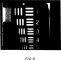
CCDsは特別に設計された、裏面入射用の開口部を有するアルミニウム窒化物回路板上に搭載された。アルミニウム窒化物が選ばれたのは、その高い熱伝導率に加え、熱膨張係数がシリコンとよく一致しているためである。リック天文台で用いられた標準パックはアルミニウム窒化物に合うように修正された。図3は−120℃で裏面入射CCDによりとられたテストパターン画像を示す。裏面電圧は25Vで、その結果基板の過空乏化が起きた。入射光の波長は400nmであった。この波長におけるシリコン内吸収深さは約0.2μmである。光子により作り出された電荷キャリアは、それ故、300μm離れたCCDポテンシャルウェルへドリフトすることになる。図3は、厚さ300μmのシリコン基板の裏面からの短波長光子を結像するために本発明によるCCDを使用した結果を示すものである。簡単に計測したところ、400nm光子に対する量子効率は約67%であった。更に、最初の計測は、25V裏面電圧における側方電荷拡散がピクセル幅であることを示している。
【0081】
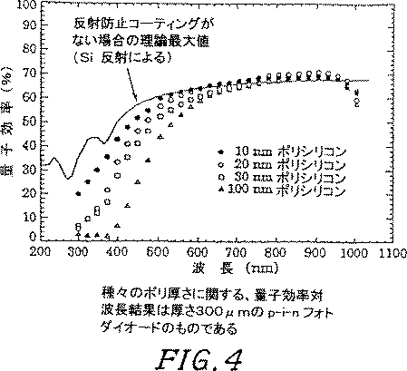
実施例7:種々の厚さの裏面層を有し、反射防止コーティングのないp−i−nフォトダイオードに関する、波長の関数としての量子効率
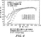
図4は、種々の厚さの裏面ポリシリコン層を有する裏面入射フォトダイオードについての、波長に対する量子効率の計測結果を示す。予想通り、短波長の応答はポリシリコンの厚さが薄くなるほど良くなる。更に、空乏化領域が比較的厚い(300μm)ために、赤外部付近の応答が波長約1μmまで伸びている。
【0082】
量子効率は、既知のスペクトル応答を持ったフォトダイオードと比較して計測した。λ=400−1100nmに対してはタングステンランプを、λ=300−450nmに対しては水銀蒸気ランプをそれぞれ使用した。光はモノクロメータを通過し、光ファイバーを通して、テストするフォトダイオード及びキャリブレーションされたフォトダイオード上に焦点を合わされた。図4は、計測した量子効率が、シリコンと空気の屈折率の不一致(シリコンの屈折率は約3.7)による反射ロスだけを想定して算出した量子効率と基本的に一致していることを示している。短い波長では、ポリシリコン接点における吸収に起因する集められた電荷のロスが、量子効率を反射限界から逸らせている。最も薄い(10nm)フィルムに関しては、量子効率の計測値が反射限界に非常に近く、λ=415nmでは、ポリシリコン層内のロスの原因となる量子効率の低下は約6%であることに留意されたい。
【0083】
実施例8:種々の厚さの裏面層を有し、反射防止コーティングのあるp−i−nフォトダイオードに関する、波長の関数としての量子効率
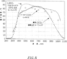
ITO反射防止コーティングの厚さは、それが対象となる波長の4分の1波長板として働くことにより反射を最小化するように選定された。即ち、
XITO=λ/4n
但し、XITOは波長λにおいて反射を最小にするフィルム厚さであり、nはITOの屈折率である。図5は、57nmのITOがコートされた10nmの裏面層を有する、裏面入射で厚さ300μmのp−i−nフォトダイオードについて、量子効率を波長の関数として示したものである(実線)。本発明によるフォトダイオードは室温で作動させた(同じくIEEE核科学)。厚さは、ルテチウム・オルトシリケート(LSO)から放射された光子の415nm波長で量子効率が最大となるように選定された。反射防止コーティングによる量子効率の改善は、100nm波長域に亘って60%を越え、λ〜450nmでピークとなり、目標値近くである。図5に示すように、薄いポリシリコン接点と4分の1波ITO層を組み合わせれば、LSO波長で約75%のQEが得られる。ビスマスゲルマニウム酸塩(BGO)に関しては、量子効率は一層高く、480nmで約90%であった。ITO厚さをBGO波長に対して最適化すれば、更に改善できるであろう。
【0084】
円形のデータ点は、約57nmのITOでコートされた、ポリシリコンの10nmの伝導裏面層を有する300μmのシリコン基板の本発明による組み合わせにより作られたCCDから採ったものである。このCCDは−120℃で作動する天体カメラに使用された。
【0085】
比較のため、薄い、低抵抗率シリコン基板上に作られた、標準的反射防止コーティングを有する従来型裏面入射CCDで採ったデータを破線で示す(M.ブルック、M.D.ネルソン「電荷結合素子のための安定した紫外線反射防止コーティング」SPIE1900、228−240、1993年)。
【0086】
実施例9:裏面電圧の関数としての電荷拡散
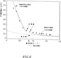
300μmの基板上に組み立てられ、厚さ50nmのITOでコートされた20nmのポリシリコンの裏面層を有するCCDを使って、幾つかの特性を計測した。その結果を下の表IIに整理して示すが、全体的には1997年2月の国際光学エンジニアリング協会会合の会報にR.J.ストーバー他の「高抵抗率シリコン上の完全空乏化CCDの特性」と題する論文(SPIEv3019、183−8頁)中で論議されており、ここに参考資料として挙げる。
先のパラグラフで述べた本発明によるCCDの裏面近くで作られた、光子に生成されたキャリアは、表面まで300μmドリフトしなければならないので、電荷の拡散と拡がりは重要な因子である。側方拡散を最小化するために、基板は、ゼロ電界領域を排除するため裏面電圧を用いて、完全に電荷空乏化される。又、裏面電圧を用いることによりドリフト電界をできるだけ高く維持することによって、300μmを横切る電子走行時間は短く保たれ、拡散を最小化する。図6は電荷の拡がり(シグマ)を裏面電圧の関数として示したものである。これは、基板が一旦完全に電荷キャリア空乏化されるとかなり弱い。電荷拡散の裏面電圧に対する依存性を調べるために、一連の小さなピンホールを有するマスクが作られた。2、4及び8μmのピンホールが使われたが、ピンホールのサイズは計測されたスポットサイズには殆ど影響を与えなかった。マスクはCCDの裏面上に直接置かれ、小さな光源から400nmの光を使って照明された。次に、裏面電圧が変えられ、画像が取られた。各スポットに対するx及びy方向の根二乗平均(RMS)の拡がりが計算され、平均が電圧の関数として図6に表示してある。一般的に、厚さ300μmのCCDの裏面電圧は25Vである(詳細はS.ホランド他「天文学及び天体物理学で使用するための裏面入射の完全空乏化CCD画像センサーの開発」電荷結合素子及び進化した画像センサーに関するIEEE研究会、ベルギー、ブルージェ、1997年6月5−7日、に述べてある)。
【0088】
このように、本発明は、高抵抗率シリコン検出器の裏面に取り付けられた電気的伝導層と、検出器の裏面と表面のパターンサイドとの間に掛けられたバイアス電圧とを提供する。電気的伝導層は、その特定の用途に応じて、(青のような)短波長光子、又は長波長光子、或いは両方に対して透過性となるように十分薄くすることができる。本発明が有用であることが分かっているデバイスには、フォトダイオード、CCDs(特に光の少ない状況に対し)、X線検出器、X線の直接検出(300μmの活性容積厚さを用いて、約5.9keVのX線までの感度が達成された)がある。原理的には、基板が厚くなるほど高エネルギーX線を検出できる。
【0089】
本発明を用いれば、デバイスに幾つかの利点が得られる。本発明による組み合わせを用いるデバイス上の光子感知容積にバイアス電圧を掛けると、出力トランジスタ特性とCCDs上のポテンシャルウェルジオメトリが改善される。更に、
・本発明によるCCD基板は表Iに示すように、Nが極端に低くなるように注文生産されており、
・基板を空乏化するために用いられる基板バイアスは、出力増幅特性と、恐らくはCCDウェルをも改善し、
・裏面ウィンドウは透過性で、電気伝導性で、要求される基板バイアスに適合でき、
・厚い光子感知容積の故にIR近傍の検出に優れ、
・現在の技術が青領域の感度を達成する場合に必要とするように薄くする必要なしに良好な青への応答性を有し、
・薄くされたCCDsと比べ曲がりが少なく、
・裏面ウィンドウを通して良好な短波長、長波長伝達を行い、
・薄くされたCCDsでは問題となる赤の縞が排除できる。
【0090】
裏面ウィンドウ層は、暗電流の顕著な増加を引き起こすことなく、高抵抗基板を完全に空乏化するに必要なバイアス電圧に耐えることができる(バイアス電圧は、高抵抗率n型基板内の少数の可動電子を取り除いて、光子によって生成された電荷が、空間解像のロスを引き起こすことになる、再結合又は拡散をする前にこれを集めるのに必要な電界となる、イオン化されたドナー原子を後に残す)。
【0091】
本発明に関わる上記説明の実施例及び最適の形態の記述は、本発明の範囲を限定する意図で行ったものではない。様々な修正、変更及びそれと同等なことが、添付する請求の範囲の精神と範囲から逸脱することなく行えるであろう。
【図面の簡単な説明】
【図1】図1は裏面入射p−i−nフォトダイオード構造で用いられる本発明による組み合わせを概略表示したものである。
【図2A】図2Aは裏面入射CCD構造で用いられる本発明による組み合わせを概略表示したものである。
【図2B】図2Bは図2Aで示されているような、高抵抗率シリコン基板上の一つのCCDのピクセルの2次元シミュレーションを示す。等電位線を0.5ボルト間隔で示している。集電ゲートには−5Vのバイアスが掛けられており、バリアフェーズは5Vにある。
【図2C】図2Cは図2Aで示されているような、高抵抗率シリコン基板上の一つのCCDの15μmのピクセルについての2次元電位分布のシミュレーションを示す。基板のドーピングは6x1011cm-3、埋め込みチャネルインプラントドーズは1.5x1012cm-2であった。
【図3】図3は、厚さ約300μmの基板を有する裏面照明CCDを使って、400nmのπ光子から作ったテストパターンの画像を示す。
【図4】図4は、厚さ300μmのp−i−nフォトダイオード上でポリシリコン裏面層の厚さを変化させた場合のQEを、波長の関数として示したものである。
【図5】図5は、厚さ300μmの基板上のポリシリコン裏面層上に57nmの反射防止コーティングを有するp−i−nフォトダイオードに関し、QEを波長の関数として示したものである(実線)。更に、厚さ300μmの基板上の本発明による裏面入射CCDに関し、QEを波長の関数として示している(円形のデータ点)。比較のため、薄い基板を有する従来型の商業ベースCCDsに関するデータも示す(破線)。
【図6】図6は電荷拡散を、厚さ300μmの基板を有するCCDにおいて、掛けられた裏面電圧の関数として示したものである。[0001]
[Technical field to which the invention belongs]
I. Background of the Invention
This invention was made with the support of the US Government under Contract No. DE-AC03-76SF00098 concerning the activities of the Lawrence Berkeley Laboratory between the US Department of Energy and the University of California. The US government has certain rights to the invention.
The present invention is disclosed in provisional application No. 60 / 030,415, and is cited here as a reference. This application claims the benefit of this provisional application filed on November 1, 1996. is there.
The present invention relates generally to electromagnetic radiation detectors, and more particularly to photosensitive silicon devices.
[0002]
[Prior art]
2. Explanation of related technology
Charge coupled devices (CCDs) were first used as memory devices for computers. Its usefulness as an image detector was developed in the 70s. James Janesic explains the general working principle of CCDs as imaging devices in his paper "CCDs: Its Inner Talk" (CCD Astronomy Winter 1997). In that paper, he also discusses the major current issues with CCD performance. Among the problems are absorption and quantum efficiency (QE) in the ultraviolet region.
[0003]
A number of techniques are used to increase the sensitivity of the blue and ultraviolet regions. The “front side” of the CCD is the side of the silicon wafer on which the electrical circuits and gates are assembled, and the “back side” is the opposite side. When a photon enters a silicon wafer (also referred to as a substrate), the photon is absorbed and generates a charge (photoelectric effect). Typically, the surface electronics are made of polycrystalline silicon (polysilicon) instead of metal, which is less reflective than metal circuitry, resulting in lower photon loss when surface incidence is used. Because. In the case of backside incidence, the image is focused on the backside, and photons generated by photoelectric action must traverse the internal thickness of the silicon substrate to the silicon area just below the surface electronics. The surface circuit is bypassed in the case of backside incidence, resulting in a high QE. Unfortunately, however, electrons do not efficiently traverse the thickness of the silicon substrate unless it is extremely thin (about 10 microns thick). Thinning the substrate to this extent is difficult, costly, and low productivity. The thinning process is described by Bark et al. In "Soft X-ray CCD imager for AXAF" (IEEE bulletin on electronic devices, 44 (10): 1633-42, 1997).
[0004]
[Problems to be solved by the invention]
Thinning the silicon substrate that forms the photosensitive volume (ie, the volume where photons are absorbed and generating charge carriers) makes it difficult to detect long wavelength photons at the same time, because thin wafers are in the red or infrared region. This is because it is transparent to photons. Long wavelength photons are not absorbed by the thin photon sensitive silicon substrate and are not detected. That is, a single conventional back-illuminator cannot be used to detect both short wavelength photons and long wavelength photons.
The sensitivity of CCDs is part of a range of functions in which the charge in each pixel can be stored without leakage of current or without external current flowing into the pixel well. A technique called pinning is used to limit dark current and affect afterimage, pixel non-uniformity, and well volume (in James Genesic, Tom Eliot's astronomical CCD observations and miniatures). “History and Evolution of Large Area Array Science CCD Imager”, Astronomical Society Pacific Conference, Vol. 23, Takson, Arizona, Book Crafts, Inc., 1992).
[0005]
[Means for Solving the Problems]
II. Summary of the Invention
The present invention is based on a combination of low resistivity or electrically conductive silicon windows that are transparent to long wavelength photons or short wavelength photons and are attached to the backside of a photon sensitive silicon layer such as a silicon wafer or chip. It is made up. This window is used for photon sensitive silicon devices such as photodiodes, charge coupled devices, active pixel sensors, low energy x-ray sensors, and other radiation detectors. A silicon window is provided on the back side of the photosensitive silicon wafer so that photons can irradiate the device from the back side without interference from circuitry printed on the front side. For this reason, it is called a back layer. When operating a device made with a combination according to the present invention, a voltage sufficient to fully deplete the high resistivity photosensitive silicon volume of charge carriers is present between the low resistivity back window and the patterned surface of the device. Hung on. This unprecedented step in operating such a photon sensing device has been made possible by the presence of an electrically conductive back layer. When a voltage is applied to the backside layer, the charge generated by the photons created on the backside can reach the surface of the device and can be processed by any circuit attached to the surface.
With the combination according to the invention, the photon sensitive silicon layer does not need to be thinner than standard manufacturing methods to achieve complete charge depletion within the silicon volume. In one embodiment, the backside window according to the present invention is applied to high resistivity silicon to allow backside incidence while maintaining charge isolation in the CCD pixel.
[0006]
DETAILED DESCRIPTION OF THE INVENTION
IV. Detailed Description of the Invention
Here, “high resistivity” means that the resistivity ρ is between 100 Ω-cm and 20 KΩ-cm for n-doped silicon, and between 100 Ω-cm and 20 KΩ-cm for p-doped silicon. It means that there is.
[0007]
Here, “substrate” means photon-sensitive silicon and does not include a circuit layer.
[0008]
Here, “substrate thickness” means the thickness of the substrate in a direction perpendicular to the plane on which the circuit is deposited on the surface.
[0009]
The present invention includes an electrically conductive, photon transmissive, layer attached to the backside of a silicon substrate. This layer is also referred to as the back window. The electrically conductive back layer or window is composed of long wavelength photons (such as red and infrared) and strongly absorbed short wavelength photons (such as blue and ultraviolet) depending on the needs of that particular application. It can be made thin enough to be permeable to both. This unprecedented combination of thin transparent conductive layers attached to a high resistivity substrate of the same thickness as a commonly produced silicon wafer (ie between 250 μm and 550 μm) is a new It is a very important component for a class of radiation detectors. When a bias voltage is applied between the back surface and the front surface of the wafer, the silicon in the middle is completely depleted of charge. The front surface circuit can detect photons that enter the back surface and generate charge. This transmissive conductive layer provides a window for back incidence of a new class of radiation detectors without the need to physically thin the intervening silicon substrate. When used in CCDs or active pixel sensors (evolved CCDs with an amplifier circuit on each pixel), fully depleted high resistivity silicon with a thickness of about 50 μm to 550 μm is near the IR region. It can be used to increase the wavelength response of the photoelectric detector (up to about 1 μ wavelength) and in the low energy X-ray region (energy between about 10 to 15 keV). Photodiodes are another type of radiation detector that would benefit from the use of the combination according to the invention.
[0010]
An electrically conductive, permeable back layer can be combined with low resistivity silicon for other applications. For example, if the conductive backside layer is applied to a CCD with a conventional thin low resistivity substrate, the backside voltage can be applied to the device. The applied voltage removes the zero electric field region on the back side of the device. Moreover, UV charging (discussed in more detail later) to keep the internal electric field in a precisely polarized state can be avoided. The applied backside voltage makes this really easy.
[0011]
FIG. 1 schematically illustrates the combination according to the invention used in a back-illuminated pin photodiode structure. Photons enter the device from the photon transmissive electrically
[0012]
Since the back layer is electrically conductive, on the other hand, when a positive voltage is applied with respect to the surface circuit, the substrate of the intermediate charge carriers can be completely depleted. This allows the dark current to be limited to a realistic level, and the charge created by the incident photons can be detected over the dark current. In addition, the application of a voltage limits the spread of charges created by photon absorption across the thickness of the substrate. Thus, when a voltage is applied, not only can the substrate of charge carriers other than those created by photon absorption be depleted, but also the resolution can be improved.
[0013]
FIG. 2A schematically shows the combination according to the invention used for back-incident charge coupled devices (CCD). Photons enter the device from the photon transmissive electrically
[0014]
FIG. 2B shows a two-dimensional simulation of one CCD pixel on a high resistivity silicon substrate as shown in FIG. 2A. Equipotential lines are shown at 0.5 volt intervals. The collector gate is biased at -5V and the barrier phase is at 5V.
[0015]
FIG. 2C shows a simulation of a two-dimensional potential distribution for a three layer 15 μm pixel. This figure shows basically the same data as shown in FIG. 2, except that it is three dimensional rather than two dimensional. 1.5x1012cm-2Channel implants are used. The substrate doping is 6 × 10 6 (corresponding to a resistivity of about 7000 Ω-cm)11cm-3It is assumed. The collecting electrode having a width of 5 μm was held at −5V, and the barrier phase was 5V. The backside bias voltage creates a drift field that extends to the backside electrical contact (y dimension in FIG. 2C).
[0016]
Applying a bias voltage to the back layer is the key to the operation of the photon detection element according to the present invention. The backside voltage completely depletes the photosensitive volume, limits charge spreading, and improves on-chip transistor characteristics. (See FIG. 2 of the IEDM paper cited later). However, this voltage must be much lower than the breakdown voltage corresponding to the electric field, and in the case of silicon, about 2 × 10 × at room temperature.FiveV / cm (SM Sze, Physics of Semiconductor Devices, 2nd Edition, John Willy and Sun, 103, 1981). High resistivity substrates with extremely few charge carriers (N) are specially fabricated so that complete charge depletion can be achieved with low backside voltage.
[0017]
If a sufficient voltage is applied, the substrate can be fully depleted of charge carriers, so that the thickness of the substrate can be much thicker than in the case of conventional back-thinned CCDs. A thick substrate has several advantages, including mechanical strength, absorption of long wavelength photons, and manufacturing economy.
[0018]
The combined substrate thickness according to the invention (8 in FIG. 1, 18 in FIG. 2A) is between about 100 μm and about 5 mm. The lower limit of the substrate thickness is preferably about 200 μm for three reasons: economic production economy, mechanical strength, and ease of electrification depletion. For economic manufacturability, for mechanical strength, and for detecting long and short wavelength photons, it is further desirable that the lower limit of the substrate thickness be about 250 microns. A 10 mm thick substrate is used for detection of high energy X-ray photons because of its long absorption length. As a practical range, the thickness of the substrate is between about 2 to 3 times the absorption length of the target photon. Therefore, for example, in order to detect a photon near the infrared region (IR), a substrate having a thickness of about 300 μm functions well.
[0019]
The thickness of the electrically conductive photon transmissive backside layer according to the present invention is partly a function of the type of radiation sensed by the detector. For short wavelength photons, the back layer must be very thin. For long wavelength photons, the back layer may be thick. A functional limitation on the thickness of the back layer is that it must be transparent to the incident photons being detected. As the back layer is progressively thickened, it becomes impermeable to short wavelength photons.
[0020]
Depending on the detector application, the conductive back layer is approximately 10nmOr a thickness between 100 μm. The thickness of the 100 μm back layer is just below the silicon band gap and is only transmissive to photons having a wavelength between about 1000 and 1100 nm. A 10 μm thick back layer is transmissive to photons having a wavelength between about 800-1100 nm. Using current deposition technology, a 10 μm polysilicon layer requires 60 hours for deposition. More generally, photon detectors according to the present invention are made with a back layer having a thickness between about 10 nm and 1 μm. The 1 μm thick back layer is transmissive to photons having a wavelength between about 550 and 1100 nm, including red and infrared regions. The backside layer of 10 to 100 nm is transmissive not only for long wavelength photons but also for blue photons, and some devices have been made with backside layers in this thickness region. The most useful range of back layer thickness is between about 10 and 50 nm, which is transparent to both short and long wavelength photons, and the time required for the deposition step is much thicker. This is because it is shorter than the layer.
[0021]
The photon absorption length in silicon depends on the temperature, and the absorption length increases as the temperature decreases. If the substrate thickness is 2 or 3 times the absorption length of the detected photon, an excessive back surface voltage is required for charge depletion. The backside voltage required for complete charge depletion increases with the square of the substrate thickness. Furthermore, if the substrate thickness is thicker than necessary for photon absorption, some loss in resolution occurs.
[0022]
In the photoelectric detector, it is important to keep the dark current low. One way to keep the dark current low is to use an in-situ doped CVD back layer that does not increase the dark current.
[0023]
The polysilicon layer is doped in situ and becomes electrically conductive. Doping is an additional element for polysilicon that increases electrical conductivity. The window layer is optically thin in order to be transparent to short wavelength light having a small absorption depth in silicon.
[0024]
There are various ways to dope polysilicon. If CVD is used, an n + layer can be secured on the backside, which is necessary for good short wavelength light absorption. Another method of doping is dopant ion implantation, but existing implanters cannot be easily implanted into such a thin (100 A) layer. Furthermore, ion implantation requires a thermal cycle that can increase dark current. Yet another doping technique is doping using thermal diffusion, but has the same problems as just described.
[0025]
Another method that can be used to dope the thin back layer is the molecular beam epitaxy method, which is very expensive. There are some advantages to doing this if cost is not an issue.
[0026]
The combination according to the invention has a particularly good long wavelength response since it is not necessary to make the silicon wafer thinner. Since the active volume (thickness of the silicon wafer) is much thicker than normal CCDs or other sensors, long wavelength photons, such as those in the infrared region, are absorbed within the active capacity of silicon and instead of passing it through Generate charge carriers.
[0027]
The thin backside polysilicon layer also acts as a transmissive electrical contact that allows for the application of a bias voltage to deplete the substrate. Since silicon has a high refractive index (3.7), the reflectivity of the layer is quite high. For example, the reflectivity is 33% at long wavelengths and much higher at short wavelengths. Applying a conductive coating that reduces the reflectivity of the back window layer increases the quantum efficiency of the combination according to the invention.
[0028]
The combination according to the invention of a transparent low resistivity back layer and a silicon wafer is further combined with an antireflection layer (10 in FIG. 1, 20 in FIG. 2). The antireflection layer is preferably electrically conductive and transmissive, for example, indium tin oxide (ITO). If in-situ doped polysilicon is coated with ITO, the reflection loss is reduced, resulting in better quantum efficiency. Using a conductive outer layer further reduces the series resistance and makes a low noise device. When the ITO coating was applied to the combination of the back layer and the silicon wafer, a dark current reduction of approximately a factor of 2 was observed.
[0029]
The ITO layer was deposited by reactive sputtering. Ionized argon atoms were attracted to the biased ITO target to sublimate the ITO molecules. The molecules are deposited on the back layer of the substrate by placing it directly opposite the ITO target.
[0030]
The main advantage of the combination according to the invention is that the back window layer is transparent to the entire spectrum of photons, including X-rays from the ultraviolet to the infrared, and the photons enter the
• Thicker devices are less susceptible to strain than thinner devices.
Apply a voltage to the back layer to create a fully charged depleted device with virtually no zero field region near the back contact (such a zero field region causes undesirably significant charge diffusion) ).
・ Red stripes, which are a problem with thin devices, are removed.
A detection device using the combination according to the invention can be back-illuminated with a good blue response corresponding to no need to be thinned.
• The active volume is not transparent to long wavelength photons.
[0031]
The thickness of the active silicon volume can be chosen to absorb and detect long-wavelength photons, while that same thickness can be used for charge carriers created by short-wavelength photons in the blue and ultraviolet regions, for example. It can lead to loss. To help detect short wavelength photons, a voltage is applied between the conductive back window layer (or optional ITO coating) and the p + region of the photodiode. In the case of a CCD or active pixel sensor, a voltage is applied between the conductive back window layer (optionally with ITO and / or other anti-reflective coating) and the polysilicon gate. The gate electrode causes a voltage drop across the buried channel, and the difference between the buried channel junction voltage and the backside voltage determines the electric field where carriers drift (for use in astronomy and astrophysics) Development of a back-illuminated fully depleted CCD image sensor "IEEE Study Group on Charge Coupled Devices and Advanced Image Sensors, Bruges, Belgium, June 5-7, 1997).
[0032]
The polysilicon layer can withstand the bias voltage required to fully deplete the high resistivity substrate without significantly increasing the dark current. The bias voltage removes a small number of mobile electrons in the high resistivity n-type substrate and the charge generated by the photons collects it before recombination or diffusion, which will cause a loss of spatial resolution. The ionized donor atoms are left behind, which is the electric field required for.
[0033]
One of the problems that can arise when applying a voltage bias between the back and front of a silicon photodevice is that voltage breakdown can occur between the pixel and an insulating structure such as a channel stop implant for CCDs. is there. The CCD column is isolated from the others by a channel stop implant, which is an ion implant that causes a greater concentration of dopant impurities on the surface of the CCD than in the volume. The effect is to create a potential barrier between adjacent columns.
[0034]
If these regions are electrically floating in the CCD, a high electric field is created between the CCD channel and the channel stop implant, which can lead to breakdown. Since the CCD channel is depleted, the potential in the channel is usually 5-10 V or more below the gate voltage applied. Channel stop implants tend to float some of the applied substrate bias, which is positive for n-type substrates.
[0035]
When a voltage is applied between the back window and the surface of the photon detection device, a fully charge depleted photon sensing volume can be created. This also improves the spatial resolution by limiting the spreading of the charge, i.e. the bloom, as the charge carriers generated by the photons move towards the detector surface.
[0036]
To avoid breakdown, a slight gap of unimplanted silicon is left between the channel and the channel stop implant. Since this region is lightly doped, the electric field is low and breakdown is avoided.
[0037]
Many of the current examples (eg CCDs, photodiodes, active pixel sensors) use n-type substrates, but this technique has also been applied to radiation detectors assembled on p-type silicon. . In that case, the insulating implant needs to compensate for the fixed charge in the silicon dioxide layer on the silicon. The absence of a fixed charge that is always positively charged results in an inversion layer of electrons that can short circuit adjacent elements.
[0038]
Bias voltage VBIs selected based on several factors including the resistance of the photon sensitive silicon capacitance.
[0039]
Available minimum bias voltage VB-MINIs equal to the depletion voltage. But from a practical standpoint, the voltage V is usually somewhat higher than the depletion voltage.BIs used. We know from experience that VB= VB-MIN+ X% (VB-MIN) Where X = N (cm in the depletion region)ThreeVariable of the number of dopant atoms per unit). When the resistance in the silicon substrate is about 10-12 kΩ-cm,B= 35V is used. Maximum VBIs limited by the presence of secondary carriers due to impact ionization of primary charge carriers, but this phenomenon is observed due to increased noise and voltage breakdown.
[0040]
Depletion voltage VDIs
VD= (0.5qN (xD)2) / ΕS
Where N is cm in the depleted region.ThreeNumber of dopant atoms per xDIs the length of the depleted region, q is the charge of the electron (1.602 10-19C), εSIs the dielectric constant of silicon (1.0 10-12F / cm). N is the resistivity,
ρ = (qμN)-1
Where ρ is the resistivity and μ is the carrier mobility (note that for lightly doped materials, the electron mobility is three times the hole mobility. For the same resistivity, N in the case of n-type silicon is three times less than that of p-type silicon).
[0041]
Depletion voltage is xDIn order to keep the depletion voltage at a reasonable value, N must be small. xDA better IR near response can be expected, and if N is smaller, the best results are obtained in both worlds, a good IR response and the possibility of back incidence under a reasonable substrate voltage.
[0042]
Table I compares ρ and N for various high resistivity CCDs (hole mobility of about 500 cm).2/ V-sec, electron mobility 1500cm2/ V-sec).
In order to deplete a substrate between 100 μm and 1000 μm with a reasonable voltage, extremely low N is required. As the above table shows, the present invention is assembled with a sufficiently low N. Other substrates, such as those with low N developed by Westinghouse researchers, exhibit extremely high dark current, much higher than can be used for normal devices. In general, if the others are the same, the lower N, the better the performance of the device according to the present invention (DM McCam et al. “Evolution in Area Array X-ray Sensor” Focal Plane Technology, SPIE Bulletin, 118- 128, 198).
[0044]
The advantage of using low N is that the substrate can be depleted at a relatively low voltage (about 20-25V). This makes breakdown problems less likely and reduces concerns about problems with one or both of the CCD pixels and the output amplifier. Both concerns are due to the strongly two-dimensional nature of extremely low N. Transistor and CCD characteristics improve with increasing backside voltage as long as the voltage stays below the breakdown voltage. The strong two-dimensional characteristics of the electric field and backside voltage make the two-dimensional electric field somewhat flat. The effect of backside voltage on the characteristics of the CCD output transistor Discussed in Holland et al., "200x200 CCD Image Sensor Made on High Resistivity Silicon" (International Electronic Devices Conference (IEDM) Technology Digest, 911-14, 1996, San Francisco, California).
[0045]
In order to obtain a sufficiently low N high resistivity silicon, German Backer Chemtronics is preparing a custom specification. The specification given to this German company is shown in the following example. W Von Amon and H Herza, in their paper “Manufacturing and Availability of High Resistivity Silicon for Use in Detectors” on the fabrication of low N high resistivity substrates (Nuclear Measurements and Methods in Physical Studies, A226, 94- 102, 1984).
[0046]
For output transistors, punch-through is a concern, and for CCD pixels, the ability to form potential wells and store charge is a concern. The insulation between pixels along a channel with a charge that spills over from one pixel to another may be poor (insensitive to channel stop implants, which insulate the channels from each other).
[0047]
If an antireflection coating is used, reflection loss can be reduced. Both silicon dioxide (an insulating material with a refractive index of 1.45) and indium tin oxide (a transmissive, refractive index 1.8-2.2 conductor) have been used successfully. There are many other things you can use.
[0048]
For photodiodes used in positron emission tomography (PET), the ITO thickness was adjusted to the desired wavelength at which the scintillating quartz crystal emits photons of a specific wavelength (S. Holland et al. “Low Noise” "Development of back-illuminated silicon photodiode arrays" IEEE Journal of Nuclear Science, 44 (3), 443-7, June 1997). About a quarter wavelength thick ITO was deposited. Another approach is to use two coatings for anti-reflective properties: an underlayer of ITO and an upper layer of silicon dioxide. Anti-reflective coating techniques are well developed and can be applied to the combined back window of the present invention. Two sources of such material and discussion are Brook and M.C. D. Nelson, “Stable UV Anti-Reflection Coating for Charge Coupled Devices” (SPIE 1900, 228-240, 1993) and M.C. Lesser's paper "Anti-reflective coating for silicon charge-coupled devices" (Optical Technology, 26 (9), 911-915, 1987).
[0049]
Films made of a class of materials called permeable conductive oxides (TCOs) provide an alternative to ITO and have similar properties. In general, any film with a low refractive index can be used as an anti-reflective coating, but high resistivity layers are undesirably non-uniform under certain circumstances, for example, very vivid images. This results in a backside voltage. Other candidate materials for antireflection coatings include hafnium oxide, lead oxide, aluminum oxide, silicon nitride, and magnesium fluoride.
[0050]
Indium tin oxide has many advantages:
[0051]
1) It is conductive and reduces the resistance of the thin backside layer (in the case of photodiodes it is important to consider noise and to create an equipotential on the backside for CCDs).
[0052]
2) Refractive index is suitable for air / ITO / silicon interface (if the intermediate film has a refractive index that is geometric intermediate between air and silicon, theoretically at a wavelength corresponding to a quarter wave plate Is zero refractive index). This is discussed in detail in the IEEE nuclear science paper cited above.
[0053]
3) It is deposited at room temperature and does not reduce leakage current.
[0054]
4) Since it is conductive, a physical back contact can be easily made.
[0055]
An insulating layer such as MgF is compatible with a thin polysilicon back layer. However, when an insulating material is used as an antireflection layer, it is necessary to remove a part of the insulating material in order to make a back contact, or to apply a voltage to the front surface and to float the back surface.
[0056]
A CCD made using a high resistivity silicon substrate as the photon sensing volume is one embodiment of the present invention. It is surprising that CCDs made of such high resistivity silicon work effectively with or without an electrically conductive layer on the back side. The high resistivity capacity makes the potential strongly two-dimensional, and many people think that the potential well will not be functionally formed in such a high resistivity material.
[0057]
Pixel is 15 × 15 μm in the device according to the invention2It is made small. It was not thought that such a small pixel could be made on a high resistivity material. Pixel size for commercial based devices on low resistivity silicon is 27x27 μm2Or 18x24μm2It is either.
[0058]
The back layer is phosphorous and is doped between about 0.0001 to 10 atomic percent doping. More preferably, it is doped with phosphorus between about 0.001 and 3 atomic percent. Most preferably, it is doped with phosphorus between about 0.1 and 3 atomic percent. The working model was made with about 1 to 1.5 atomic percent phosphorus doping and without annealing. Details are described in the IEEE bulletin on nuclear science cited above.
[0059]
Surface pinning. The dark current of a CCD has both a bulk component and a surface component. Effective gettering from a phosphorous doped polysilicon layer can greatly reduce the bulk component while leaving the surface component as the main source of dark current.
[0060]
Techniques for reducing surface current include filling the surface interface state with carriers supplied from a channel stop implant. The polysilicon gate electrode in front of the device is biased so that a carrier inversion layer is created to fill the surface state. Once satisfied, this state no longer contributes to dark current. Movable carriers are concentrated on the surface and the potential is nailed, which is called surface pinning. This technique requires that the channel stop implant be biased (usually at ground potential).
[0061]
For a fully depleted CCD, there may be an ohmic path between the bias applied to the back window and the channel stop contact outside the CCD itself, and the result is between the back and the channel stop. A large current will flow through. Using a simple diode structure with an appropriate geometry (ie n + contacts on the front side must be surrounded by p + or CCD pixels must be on both sides), the channel stop current is reduced. This geometry design reverse biases the channel stop via a nearby pn junction.
[0062]
There are other techniques that can significantly reduce the surface current when used in combination with the CCD geometry described above. Long emission times at low temperatures trap carriers in the surface state. First, a channel stop is connected to the carrier, and the surface state is satisfied under the condition that all CCD gates are held at a potential sufficient to reverse the surface carrier type. The channel stop contact is then floated and the long emission time constant keeps the surface current low during the operation of the CCD.
[0063]
Unreliable techniques such as UV charging to keep the electric field in the correct direction on the backside can be avoided using the present invention because the voltage applied to the backside layer of the present invention eliminates this problem ( "200x200 CCD image sensor made on high resistivity silicon" International Electronic Device Conference (IEDM) Technology Digest, 911-14, 1996, San Francisco, California).
[0064]
The problem is that natural oxides form naturally on silicon. The oxide on silicon always has a certain positive charge at the interface. In normally used p-type silicon, this positive charge forms a small depletion layer on the back surface. For short wavelength photons, this constant charge is added to the generated electrons towards the back. The solution is backside UV charging that creates a surface layer of electrons to overcome this constant positive charge. Another technique is a flash gate in which the work function of a thin transmissive gate overcomes the positive charge.
[0065]
In another attempt to solve this problem, RCA researchers have reflected holes towards the potential well with a conventional low resistivity CCD on n-type silicon where positive charge is applied. If this invention is used, this problem will be solved if the backside voltage is applied. Even when the CCD is made of a p-type substrate, if the present invention is used, a sufficiently large back surface voltage sufficient to deplete the substrate of charge is more than compensating for the positive charge.
[0066]
There are several important parameters for the radiation sensitive device according to the invention.
The back layer is doped with phosphorus between about 0.0001 to 10 atomic percent doping. More preferably, it is doped with phosphorus between about 0.001 and 3 atomic percent. Most preferably, it is doped with phosphorus between about 0.1 and 3 atomic percent. The working model was built without annealing, using about 1 atomic percent phosphorus doping.
For n-type substrates, the resistivity of the substrate used for the photon sensing volume may be between about 100 Ω-cm and about 20 KΩ-cm. More desirably, it is between about 6 KΩ-cm and about 12 KΩ-cm.
For the p-type substrate, the resistivity of the silicon substrate used for the photon sensing volume may be between about 100 KΩ-cm and about 20 KΩ-cm. More desirably, it is between about 6 KΩ-cm and 15 KΩ-cm.
The bias voltage applied between the electrically conductive backside layer according to the invention and the conductive region on the surface of the photon sensitive silicon volume is due to the voltage breakdown with the upper end across the silicon volume and the lower end due to the carrier velocity generated by the bias. Limited. The carrier velocity across the silicon volume must be large enough to overcome the radial carrier movement due to thermal diffusion.
As the resistivity decreases (of the silicon substrate used for the photon sensing volume), the voltage required for full depletion decreases. If the photosensitive volume silicon resistance becomes too low, the bias voltage will cause breakdown or excessive noise before the condition is depleted.
As the resistivity (of the silicon substrate used for the photon sensing volume) increases, the geometry of the potential well under the CCD gate becomes more two-dimensional and the transistor characteristics degrade. This phenomenon limits the maximum resistivity that can be used with silicon substrates. The two-dimensional effect can be partially compensated by increasing the backside voltage. When the backside voltage exceeds the depletion voltage, two terms describe the electric field (see
The thickness of the electrically conductive back layer according to the invention is partly a function of the type of radiation sensed by the detector. For short wavelength photons, the back layer must be very thin. For long wavelength photons, the back layer may be thick. A functional limitation on the thickness of the back layer is that it must be transparent to the incident photons to be detected. As the back layer is progressively thickened, it becomes impermeable to short wavelength photons. The back layer has been successfully made to have a thickness between about 10 nm and about 1000 μm depending on the detector application. More preferably, the back layer should be between about 10 nm and about 100 μm to minimize leakage current.
[0067]
Example 1: Production of back window
The back window according to the present invention comprises phosphine (PHThreeIn the presence of silane (SiH) on a high resistivity silicon substrate.Four) By low pressure chemical vapor deposition (CVD). This treatment is performed at a low temperature, ie, about 650 ° C., in an extremely clean environment, and impurities are kept at 1 billionth or less. Since this is a low temperature process, the deposition of the polycrystalline silicon (polysilicon) layer occurs near the end of the process after all the high temperature processing is complete. The following process protocol shows one sequence for applying windows. The side walls of the vacuum chamber are covered with polysilicon deposited on the chamber walls. The purity of the gas used is 99.999%. The silicon wafer is pre-cleaned according to the required protocol, if generally accepted. The substrate is subjected to a gettering process before the back window is deposited. Thick, phosphorus doped polysilicon is used for gettering and then etched before the back window is deposited. The gettering process is the same as that described in S.A. This is done according to the method published by Holland in nuclear measurements and methods in 1989 physics research entitled "Manufacture of detectors and transistors on high resistivity silicon", pages A275, 537-541. This process provides a substrate that is substantially free of metal contaminants.
[0068]
The back layer is doped with phosphorus between about 0.0001 to about 10 atomic percent doping. More preferably, it is doped with phosphorus between about 0.001 and about 3 atomic percent. Most preferably, it is doped with phosphorus between about 0.1 and about 3 atomic percent. The working model was created using about 1 atomic percent phosphorus doping.
[0069]
Basically, the deposition of a thin backside polysilicon window is performed in the following steps.
a. Standard pre-diffusion clean with final diluted HF etch followed by DI rinse.
b. LPCVD of doped polysilicon on wafer backside using therm co-recipe DPOLY.
c. Measurement of polysilicon thickness on monitor wafer.
[0070]
Processing is at a temperature of about 650 ° C., a pressure of 400 mTorr,Four
[0071]
Example 2: Obtaining a low-N substrate
Bids were obtained from several candidate wafer manufacturers to obtain the desired high resistivity, low N silicon wafers. The wafers used for most of the experiments described here are custom-made from Wacker Siltronic, a district sales office (95117, California, San Jose, # 114, Mall Park Street 4010, 408 / 554-9728). is there. The wafer was manufactured according to the following specifications.
1. Type: n-type, phosphorus doping, float zone impurity removal, no transition
2. Crystal orientation: <100>
3. Resistivity: 6000 Ω-cm or more, preferably around 10,000 Ω-cm
4). Minor carrier life: 1 ms or more
5. Diameter: 100mm
6). Nominal thickness: 300 μm
7). Flatness: According to SEMI standard
8). Edge: The edge is rounded to minimize edge cracking that can lead to wafer breakage during handling.
9. Wafer finish: polishing on one side, no damage on the other side, ie no intentional damage or gettering on the back side.
10. Thickness tolerance: +/− 15 μm max.
11. Taper: <5 μm max.
12 Bending: <30 μm max.
13. Quantity: 500 wafers
[0072]
Example 3: Fabrication of a photodiode having an electrically conductive, photon transmissive backside layer
The following process flow was used to fabricate a back-illuminated photodiode having an electrically conductive, photon transmissive polysilicon layer on the back side on an n-type substrate. An updated protocol is available from the inventor of Lawrence Berkeley National Laboratory, Berkeley, California, telephone 510 / 486-4000.
[0073]
Starting material: silicon wafer for substrate of
(1) Low temperature oxide deposition
a. Standard pre-diffusion cleaning
Piranha (WPS2) for 5 minutes at 110 ° C
DI water rinse (WPS2)
Diluted HF etching (WPS2)
DI water rinse (WPS2)
Megasonic RCA I wash (WPS2) for 5 minutes at 40 ° C
DI water rinse (WPS2)
Diluted HF etching (WPS2)
DI water rinse (WPS1)
Megasonic RCA II wash (WPS1) for 5 minutes at 40 ° C
DI water rinse (WPS1)
b. 5000A SiO2Of LPCVD and thermco recipe UDLTO at 425 ° C for 30 minutes
c. Measurement of oxide thickness on monitor wafer
(2) Backside oxide removal
a. Prepare wafer on LP3 (HMDS application)
b. Spin OCG825 photoresist (MTI recipe # 1)
c. Hard bake wafers at 120 ° C for 30 minutes
d. Etch wafer with 6: 1 buffered oxide etch (BOE) until backside oxide is completely removed
e. Strip resist in Piranha (WSP5)
(3) 1 μm in-situ doped polysilicon deposition
a. Standard pre-diffusion clean with final diluted HF etch followed by DI rinse.
b. LPCVD of doped polysilicon on wafer backside, about 6 hours deposition using thermco-recipe DPOLY
c. Polysilicon thickness measurement on monitor wafer
(4) 1000A nitride deposition
a. Pre-diffusion cleaning, but not required if wafer is loaded into nitride tube immediately following deposition of doped polysilicon
b. 47 minutes deposition using LPCVD of 1000A silicon nitride on the backside of wafer and thermco recipe NITRIDE
(5) Surface nitride / poly removal
a. Technique c Plasma etch of surface nitride / poly using etcher on campus. 100W, 280 mTorr, 13 sccm SF621 sccm He.
(6) Surface LTO removal
a. Etching surface LTO with BOE
(7) 4000A field oxidation
a. Standard pre-diffusion cleaning
b. Steam oxidation to grow 4000A field oxide, using Thermoco recipe WET 4000A, tube 2-1, 4 hours 45 minutes at 900 ° C, TCA cleaning of furnace tube using Thermoco recipe 1TCACCN before oxidation
c. Measure oxide thickness on monitor wafer
(8) Mask 1 (p + implant)
a. Prepare wafer on LP3 (HMDS application)
b. Spin OCG825 photoresist (MTI recipe # 1)
c. Exposure using mask 1 (0.6 second exposure)
d. Developed with 3: 1 DI water: OCG809 (WPS3)
e. Inspection
(9) Oxide etching
a. Hard bake wafers at 120 ° C for 30 minutes
b. Determine etch rate of 6: 1 buffered oxide etch (BOE) rate using 1000A thermal oxide test wafer
c. The required etching time is calculated based on the BOE etching rate and measured thickness. In addition to all the time required for wetting, add 20% to this time and etch the wafer.
d. After DI water rinse, test hydrophobic surface behavior on large etched surface. Measure residual oxide thickness with nano specs to ensure complete oxide removal.
e. Strip resist in Piranha (WPS5)
(10) Boron implant
a.
(11) 1000A thermal oxidation / implant annealing
a. Standard pre-diffusion cleaning:
b. Steam oxidation to grow 1000 A field oxide (37 minutes at 900 ° C.), followed by 2 hour nitride anneal, Thermoco recipe W1000DET, tube 2-1, before thermal oxidation, TCA of furnace tube using Thermocorecipe 1TCACCN Washing
c. Measure oxide thickness on monitor wafer
(12) Removal of backside oxynitride / nitride
a. Prepare wafer on LP3 (HMDS application)
b. Spin OCG825 photoresist (MTI recipe # 1)
c. Hard bake wafers at 120 ° C for 30 minutes
d. Etch wafer for 3 minutes with 6: 1 buffered oxide etch (BOE) to remove backside oxide
e. Strip resist in Piranha (WPS5)
f. Remove backside nitride in phosphoric acid at 190 ° C
(13) Removal of backside polysilicon
a. Prepare wafer on LP3 (HMDS application)
b. Spin OCG825 photoresist (MTI recipe # 1)
c. Hard bake wafers at 120 ° C for 30 minutes
d. Etch wafer with silicon etch until backside polysilicon and diffused n + layer is removed. Use a monitor wafer from the backside poly deposition to determine an appropriate etching time, and confirm removal by 4-point probe measurement on the backside wafer.
(14) Thin backside polysilicon deposition
a. Standard pre-diffusion clean with final diluted HF etch followed by DI rinse.
b. LPCVD of doped polysilicon on the backside of the wafer using the Samco Recipe DPOLY,
c. Polysilicon thickness measurement on monitor wafer
(15) Surface polysilicon removal
a. Technique c Plasma etch of surface polysilicon using etcher on campus. 100W, 280 mTorr, 13 sccm SF621 sccm He. Minimizing over-etching due to the relatively poor sensitivity of this etch to oxide.
b. Cleaning the wafer with Piranha (WPS5)
(16) Mask 2 (contact mask)
a. Prepare wafer on LP3 (HMDS application)
b. Spin OCG825 photoresist (MTI recipe # 1)
c. Exposure using mask 4 (0.6 second exposure)
d. Developed with 3: 1 DI water: OCG809 (WPS3)
e. Inspection
(17) Contact etching
a. Hard bake wafers at 120 ° C for 30 minutes
b. Determine etch rate of 6: 1 buffered oxide etch (BOE) rate using low temperature oxide monitor wafer
c. The required etching time is calculated based on the BOE etching rate and measured thickness. In addition to all the time required for wetting, add 20% to this time and etch the wafer.
d. After DI water rinse, test hydrophobic surface behavior on large etched surface. Measure residual oxide thickness with nano specs to ensure complete oxide removal.
e. Strip resist in Piranha (WPS5)
(18) 0.5 μm aluminum deposition
a. Determines the etching rate of diluted HF bath
b. Etching to remove 60A oxide based on etch rate measurement
c. Load wafer into MRC603
d. Sputtering aluminum at 6kW, 15cm / sec, 10mTorr
(19) Mask 5 (melting mask)
a. Prepare wafer on LP3 (HMDS application)
b. Spin OCG825 photoresist (MTI recipe # 1)
c. Exposure using mask 5 (0.6 second exposure)
d. Developed with 3: 1 DI water: OCG809 (WPS3)
e. Inspection
(20) Metal etching
a. Hard bake wafers at 120 ° C for 30 minutes
b. Etch wafer in aluminum etchant at 30 ° C
c. Removal of silicon residue by campus technique c plasma etcher
d. Strip resist with PRS-2000 (WPS5)
(21) Sintering
a. Sintered at 400 ° C in molding gas using Samco Recipe SINT400, tube 1-2
(22) Backside ITO deposition / annealing
See Example 5
[0074]
Example 4 CCD
The following process flow was used to fabricate a back-incident charge-coupled device having an electrically conductive, photon transmissive polysilicon layer on the back side on an n-type substrate.
[0075]
Starting material: silicon wafer for substrate of
(1) Low temperature oxide deposition
a. Standard pre-diffusion cleaning
Piranha (WPS2) for 5 minutes at 100 ° C
DI water rinse (WPS2)
Diluted HF etching (WPS2)
DI water rinse (WPS2)
Megasonic RCA I wash (WPS2) for 5 minutes at 40 ° C
DI water rinse (WPS2)
Diluted HF etching (WPS2)
DI water rinse (WPS1)
Megasonic RCA II wash at 45 ° C for 5 minutes (WPS1)
DI water rinse (WPS1)
b. 5000A SiO2Of LPCVD and thermco recipe UDLTO at 425 ° C for 30 minutes
c. Measurement of oxide thickness on monitor wafer
(2) Backside oxide removal
a. Prepare wafer on LP3 (HMDS application)
b. Spin OCG825 photoresist (MTI recipe # 1)
c. Hard bake wafers at 120 ° C for 30 minutes
d. Recoat with OCG825 photoresist (MTI recipe # 1)
e. Hard bake wafers at 120 ° C for 30 minutes
f. Etch wafer with 6: 1 buffered oxide etch (BOE) until backside oxide is completely removed
g. Strip resist in Piranha (WSP5)
(3) 1 μm in-situ doped polysilicon deposition
a. Standard pre-diffusion clean with final diluted HF etch followed by DI rinse.
b. LPCVD of doped polysilicon on wafer backside, about 6 hours deposition using thermco-recipe DPOLY
c. Polysilicon thickness measurement on monitor wafer
(4) 1000A nitride deposition
a. Pre-diffusion cleaning, but not required if wafer is loaded into nitride tube immediately following deposition of doped polysilicon
b. 47-minute deposition using LPCVD of 1000A silicon nitride on the backside of wafer and thermco recipe NITRIDE
(5) Surface nitride / poly removal
a. Technique c Plasma etch of surface nitride / poly using etcher on campus. 100W, 280 mTorr, 13 sccm SF621 sccm He.
(6) Surface LTO removal
a. Etching surface LTO with BOE
(7) 500A gate oxidation
a. Standard pre-diffusion cleaning
b. Dry the oxide with TCA to grow 500A gate oxide, use Thermoco recipe D200GATW, tube 2-2 for 3 hours 45 minutes at 900 ° C, TCA clean the furnace tube with thermco recipe 1TCACCN before oxidation
c. Measurement of oxide thickness on monitor wafer
d. Load wafers quickly into nitriding furnace
(8) 500A nitride deposition
a. The wafer is loaded directly from the gate oxidation furnace, so no cleaning is required
b. 500A nitride deposition, thermco recipe NITCCD, 20.5 minutes deposition using tube 2-4
c. Measurement of nitride thickness on monitor wafer
(9) Mask 1 (active area mask)
a. Prepare wafer on LP3 (HMDS application)
b. Spin OCG825 photoresist (MTI recipe # 1)
c. Exposure using mask 4 (0.6 second exposure)
d. Developed with 3: 1 DI water: OCG809 (WPS3)
e. Inspection
(10) Nitride etching
a. Hard bake wafers at 120 ° C for 30 minutes
b. Technique c Nitride etching using plasma etcher on campus. Set an appropriate etching time, etch half of that time, rotate the wafer 180 degrees, and etch the other half (improves etching uniformity)
c. Do not remove resist
(11) Field implant (phosphorus)
a. 1 · 1012cm-2Dose, 30 keV energy (irradiation range about 0.15 μm), 7 degree tilt angle (target: 250 V field threshold voltage with 0.5 μm oxide thickness)
(12) Resist / oxide removal
a. Strip resist in Piranha
b. Etch residual oxide with 6: 1 BHF after plasma etching
(13) 4500A field oxidation
a. Standard pre-diffusion cleaning:
b. Steam oxidation to grow 4500A field oxide, thermco recipe WET4500A, tube 2-1 for 5 hours at 450 ° C., TCA clean of furnace tube using thermco recipe 1TCACLN before oxidation
c. Measure oxide thickness on monitor wafer
(14) Mask 2 (channel mask)
a. Prepare wafer on LP3 (HMDS application)
b. Spin OCG825 photoresist (MTI recipe # 1)
c. Exposure using mask 2 (0.6 second exposure)
d. Developed with 3: 1 DI water: OCG809 (WPS3)
e. Inspection
(15) Channel implant (boron)
a. 1.0, 1.5, and 2.0 · 1012cm-2Dose, 150 keV energy (irradiation range approx. 0.4 μm), 7 degree tilt angle
(16) Resist removal
a. Remove resist with Piranha
(17) Polysilicon-1 deposition
a. Standard pre-diffusion cleaning.
b. LPCVD of undoped polysilicon, 4500A. Recipe POLY4500, 53.5 minutes deposition at 615/620/630 ° C., 40 sccm silane pre / post flow, 200 mTorr pressure
c. Polysilicon thickness measurement on monitor wafer
(18) Polysilicon-1 implant (boron)
a. 2.0.1015cm-2Dose, 150 keV energy (irradiation range approx. 0.2 μm), 7 degree tilt angle
(19) Mask 3 (polysilicon-1 mask)
a. Prepare wafer on LP3 (HMDS application)
b. Spin OCG825 photoresist (MTI recipe # 1)
c. Exposure using mask 3 (0.6 second exposure)
d. Developed with 3: 1 DI water: OCG809 (WPS3)
e. Inspection
(20) Polysilicon-1 etching
a. Hard bake wafers at 120 ° C for 30 minutes
b. Etching
c. Strip resist with oxygen plasma, then piranha cleaning
(21) Removal of backside polysilicon-1
a. Prepare wafer on LP3 (HMDS application)
b. Spin OCG825 photoresist (MTI recipe # 1)
c. Hard bake wafers at 120 ° C for 30 minutes
d. Recoat with OCG825 photoresist (MTI recipe # 1)
e. Hard bake wafers at 120 ° C for 30 minutes
f. Etching poly in silicon etchant
g. Strip resist in Piranha
(22) Polysilicon-1 oxidation
a. Standard pre-diffusion cleaning by final HF etching
b. Wet oxidation with TCA to grow 1700A interpoly oxide, use Thermoco recipe POLY2K, tube 2-1, 30 minutes at 950 ° C, TCA clean furnace tube with Thermocorecipe 1TCACCN before oxidation
c. Oxide thickness measurement on monitor wafer using campus nanoduv
(23) Polysilicon-2 deposition
a. No cleaning is required if the wafer is loaded directly from the oxidation tube
b. LPCVD of undoped polysilicon, 4500A. Recipe POLY4500, 53.5 minutes deposition at 615/620/630 ° C., 40 sccm silane pre / post flow, 200 mTorr pressure
c. Polysilicon thickness measurement on monitor wafer
(24) Polysilicon-2 implant (boron)
a. 2.0.1015cm-2Dose, 80 keV energy (irradiation range approx. 0.2 μm), 7 degree tilt angle
(25) Mask 4 (polysilicon-2 mask)
a. Prepare wafer on LP3 (HMDS application)
b. Spin OCG825 photoresist (MTI recipe # 1)
c. Exposure using mask 4 (0.6 second exposure)
d. Developed with 3: 1 DI water: OCG809 (WPS3)
e. Inspection
(26) Polysilicon-2 etching
a. Hard bake wafers at 120 ° C for 30 minutes
b. Etching
c. Strip resist with oxygen plasma, then piranha cleaning
(27) Removal of backside polysilicon-2
a. Prepare wafer on LP3 (HMDS application)
b. Spin OCG825 photoresist (MTI recipe # 1)
c. Hard bake wafers at 120 ° C for 30 minutes
d. Recoat with OCG825 photoresist (MTI recipe # 1)
e. Hard bake wafers at 120 ° C for 30 minutes
f. Etching poly in silicon etchant
g. Strip resist in Piranha
(28) Polysilicon-2 oxidation
a. Standard pre-diffusion cleaning by final HF etching
b. Wet oxidation with TCA to grow 1700A interpoly oxide, use Thermoco recipe POLY2K, tube 2-1, 30 minutes at 950 ° C, TCA clean furnace tube with Thermocorecipe 1TCACCN before oxidation
c. Oxide thickness measurement on monitor wafer using campus nanoduv
(29) Polysilicon-3 deposition
a. No cleaning is required if the wafer is loaded directly from the oxidation tube
b. LPCVD of undoped polysilicon, 4500A. Recipe POLY4500, 53.5 minutes deposition at 615/620/630 ° C., 40 sccm silane pre / post flow, 200 mTorr pressure
c. Polysilicon thickness measurement on monitor wafer
(30) Polysilicon-3 implant (boron)
a. 2.0.1015cm-2Dose, 80 keV energy (irradiation range approx. 0.2 μm), 7 degree tilt angle
(31) Mask 5 (polysilicon-3 mask)
a. Prepare wafer on LP3 (HMDS application)
b. Spin OCG825 photoresist (MTI recipe # 1)
c. Exposure using mask 5 (0.6 second exposure)
d. Developed with 3: 1 DI water: OCG809 (WPS3)
e. Inspection
(32) Polysilicon-3 etching
a. Hard bake wafers at 120 ° C for 30 minutes
b. Etching
c. Strip resist with oxygen plasma, then piranha cleaning
(33) Removal of backside polysilicon-3
a. Prepare wafer on LP3 (HMDS application)
b. Spin OCG825 photoresist (MTI recipe # 1)
c. Hard bake wafers at 120 ° C for 30 minutes
d. Recoat with OCG825 photoresist (MTI recipe # 1)
e. Hard bake wafers at 120 ° C for 30 minutes
f. Etching poly in silicon etchant
g. Strip resist in Piranha
(34) Polysilicon-3 oxidation
a. Standard pre-diffusion cleaning by final HF etching
b. Wet oxidation with TCA to grow 1700A interpoly oxide, thermco recipe POLY1K, tube 2-1, 30 minutes at 900 ° C, TCA clean of furnace tube with thermco recipe 1TCACLN before oxidation
c. Measurement of oxide thickness on monitor wafer
(35) Mask 6 (substrate contact mask)
a. Prepare wafer on LP3 (HMDS application)
b. Spin OCG825 photoresist (MTI recipe # 1)
c. Exposure using mask 6 (0.6 second exposure)
d. Developed with 3: 1 DI water: OCG809 (WPS3)
e. Inspection
(36) Oxide etching
a. Hard bake wafers at 120 ° C for 30 minutes
b. Determine etch rate of 6: 1 buffered oxide etch (BOE) rate using 1000A thermal oxidation test wafer
c. The required etching time is calculated based on the BOE etching rate and measured thickness. In addition to all the time required for wetting, add 20% to this time and etch the wafer.
d. After DI water rinse, test hydrophobic surface behavior on large etched surface. Measure residual oxide thickness with nano specs to ensure complete oxide removal.
e. Strip resist in Piranha (WPS5)
(37) Mask 7 (substrate contact implant)
a. Prepare wafer on LP3 (HMDS application)
b. Spin OCG825 photoresist (MTI recipe # 1)
c. Exposure using mask 7 (0.6 second exposure)
d. Developed with 3: 1 DI water: OCG809 (WPS3)
e. Inspection
(38) Substrate contact implant
a. Phosphorus, P+2.0 / 1015cm-2Implants in hybrid mode to limit substrate heating, 100 keV energy, 7 degree tilt angle
b. Strip the resist with oxygen plasma, followed by piranha cleaning
(39) Mask 8 (floating electrode, source / drain implant)
a. Prepare wafer on LP3 (HMDS application)
b. Spin OCG825 photoresist (MTI recipe # 1)
c. Exposure using mask 8 (0.6 second exposure)
d. Developed with 3: 1 DI water: OCG809 (WPS3)
e. Inspection
(40) Nitride etching
a. Plasma etch nitride using technique c etcher on campus
b. Do not remove resist
(41) Floating electrode, source / drain implant
a.
b. Strip the resist with oxygen plasma, followed by piranha cleaning
(42) 5000A oxide deposition (LTO / BPSG)
a. Standard pre-diffusion cleaning
b. SiO2500A LPCVD, 30 minutes deposition at 425 ° C using thermco recipe UDLTO
c. Measurement of oxide thickness on monitor wafer
(43) High temperature forming gas annealing
a. Standard pre-diffusion cleaning
b. 1 hour using thermco-recipe FGANNNEAL, tube 1-1, anneal at 950 ° C. in the forming gas, TCA clean the furnace tube using thermco-recipe 1TCACLN before oxidation
c. Measurement of oxide thickness on monitor wafer
(44) Removal of backside oxynitride / nitride
a. Prepare wafer on LP3 (HMDS application)
b. Spin OCG825 photoresist (MTI recipe # 1)
c. Hard bake wafers at 120 ° C for 30 minutes
d. Recoat with OCG825 photoresist (MTI recipe # 1)
e. Hard bake wafers at 120 ° C for 30 minutes
f. Etch wafer in 6: 1 buffered oxide etch (BOE) for 5 minutes to remove backside LTO / oxynitride
g. Strip resist in Piranha (WPS5)
f. Remove backside nitride in phosphoric acid at 190 ° C. Note that an intermediate dilution HF etch may need to be performed to remove the oxynitride between the cap and gate nitride.
(45) Backside polysilicon removal
a. Prepare wafer on LP3 (HMDS application)
b. Spin OCG825 photoresist (MTI recipe # 1)
c. Hard bake wafers at 120 ° C for 30 minutes
d. Recoat with OCG825 photoresist (MTI recipe # 1)
e. Hard bake wafers at 120 ° C for 30 minutes
f. The wafer was n-diffused with backside polysilicon during silicon etching.+Etch until the layer is removed. In order to determine the appropriate etching time, a monitor wafer from the backside poly deposition was used, and removal was confirmed by 4-point probe measurement on the backside of the wafer.
(46) Thin backside polysilicon deposition
a. Added final diluted HF etching and subsequent DI rinse to standard pre-diffusion cleaning
b. LPCVD of doped polysilicon on the backside of the wafer using the Samco Recipe DPOLY
c. Measurement of polysilicon thickness on monitor wafer
(47) Surface polysilicon removal
a. Technique c Plasma etch of surface poly using etcher on campus. 100W, 280 mTorr, 13 sccm SF621 sccm He. Minimizing over-etching due to the relatively poor sensitivity of this etch to oxide.
b. Cleaning the wafer with Piranha (WPS5)
(48) Mask 9 (contact mask)
a. Prepare wafer on LP3 (HMDS application)
b. Spin OCG825 photoresist (MTI recipe # 1)
c. Exposure using mask 9 (0.6 second exposure)
d. Developed with 3: 1 DI water: OCG809 (WPS3)
e. Inspection
(49) Contact etching
a. Hard bake wafers at 120 ° C for 30 minutes
b. Determine etch rate of 6: 1 buffered oxide etch (BOE) rate using low temperature oxide monitor wafer
c. The required etching time is calculated based on the BOE etching rate and measured thickness. In addition to all the time required for wetting, add 20% to this time and etch the wafer.
d. After DI water rinse, test hydrophobic surface behavior on large etched surface. Measure residual oxide thickness with nano specs to ensure complete oxide removal.
e. Strip resist in Piranha (WPS5)
(50) 0.5 μm aluminum deposition
a. Determines the etching rate of diluted HF bath
b. Etching to remove 60A oxide based on etch rate measurement
c. Load wafer into MRC603
d. Sputtering aluminum at 6kW, 15cm / sec, 10mTorr
(51) Mask 10 (metal mask)
a. Prepare wafer on LP3 (HMDS application)
b. Spin OCG825 photoresist (MTI recipe # 1)
c. Exposure using mask 10 (0.6 second exposure)
d. Developed with 3: 1 DI water: OCG809 (WPS3)
e. Inspection
(52) Metal etching
a. Hard bake wafers at 120 ° C for 30 minutes
b. Etch wafer in aluminum etchant at 30 ° C
c. Removal of silicon residue by campus technique c plasma etcher
d. Strip the resist with PRS-2000
(53) Sintering
a. Sintered at 400 ° C in molding gas using Samco Recipe SINT400, tube 1-2
(54) Backside ITO deposition / annealing
See Example 5 below
[0076]
Example 5: Deposition of ITO layer
The ITO layer is 90% by weight In at room temperature.2OThreeAnd 1 wt% SnO2Vapor deposition was performed by magnetron sputtering from a target (target surface is 12 cm × 38 cm). The power used for the entire deposition was 500W. Conduction in ITO is due to oxygen vacancies and therefore the oxygen concentration in the film must be well controlled. Reported in Lee et al., “Electronic and optical properties of room temperature sputtering deposited indium tin oxide” (J. Vac. Chemistry and Technology, A-11, 5, 2742-6, September / October 1993). The film is O2Sputtered reactively in a mixture of Ar and Ar. To determine the deposition conditions that give the film low resistivity and high optical transmission, the total sputter pressure is changed to 2-8 mTorr, O2The concentration was changed to 0-5%.
[0077]
A thickness-independent quantity R to account for both resistivity and transmittance when evaluating film quality□In (1 / t) is used as a performance coefficient, but here R□Is the sheet resistance and t is the optical transmission at a given wavelength. The sheet resistance of the film was measured using a four-point probe, and the optical transmittance was measured using a dual beam spectrophotometer with a tungsten halogen lamp. During film deposition, O2When plotted as a function of the partial pressure of R, R□In (1 / t) shows a noticeable minimum and the best film is O2Was obtained at a partial pressure of 0.04-0.08 mTorr.
[0078]
As the back contact to the photodiode array, ITO has a total pressure of 2 mTorr, O2Deposition was performed at a partial pressure of 0.06 mTorr. In this deposited state, the resistivity of the film is about 4.8 × 10-FourIt was Ω-cm. Low temperature, post-deposition annealing further improves film quality, N2As a result of annealing at 200 ° C. for 1 hour, the resistivity is about 3.4 × 10-FourIt decreased to Ω-cm. When the Hall effect on ITO was measured before and after annealing, the carrier density was 6.7 × 1020cm-3To 8.7x1020cm-3The carrier mobility is 19cm2/ V-sec to 21cm2It slightly changed to / V-sec. Further, the transmittance of the film having a thickness of 54.5 nm is increased by S.E. As shown in FIG. 3 of Holland et al., “Low Noise, Back-Injected Silicon Photodiode Array” (IEEE Journal on Nuclear Science, 44 (3), 443-7, June 1997). In particular, the transmission is rising just below the wavelength of 400 nm, which probably indicates an increase in the energy gap of the material. The transmittance at λ = 415 nm, which is the wavelength at the peak emission for lutetium orthosilicate, increased from 73% to 83%.
[0079]
Example 6: Test pattern image using 400 nm light
CCDs were fabricated with a 20 nm backside polysilicon layer. Further, an anti-reflective coating of about 50 nm of ITO was sputter deposited on polysilicon (S. Holland et al. “Low Noise, Back-Injected Silicon Photodiode Array” (IEEE Journal of Nuclear Science, 44 (3), 443- 7, June 1997)). This layer was electrically conductive and, in addition to acting as an anti-reflective coating, reduced the resistance of the back contact.
[0080]
The CCDs were mounted on a specially designed aluminum nitride circuit board with an opening for back incidence. Aluminum nitride was chosen because its thermal expansion coefficient is in good agreement with silicon in addition to its high thermal conductivity. The standard pack used at the Rick Observatory was modified to fit aluminum nitride. FIG. 3 shows a test pattern image taken by a back-thinned CCD at −120 ° C. The backside voltage was 25V, resulting in depletion of the substrate. The wavelength of the incident light was 400 nm. The absorption depth in silicon at this wavelength is about 0.2 μm. Charge carriers created by photons will therefore drift to CCD
[0081]
Example 7: Quantum efficiency as a function of wavelength for pin photodiodes with back layers of varying thickness and without anti-reflective coating
FIG. 4 shows the measurement results of quantum efficiency with respect to wavelength for back-illuminated photodiodes having backside polysilicon layers of various thicknesses. As expected, the short wavelength response improves with decreasing polysilicon thickness. Furthermore, since the depletion region is relatively thick (300 μm), the response near the infrared region extends to a wavelength of about 1 μm.
[0082]
The quantum efficiency was measured in comparison with a photodiode with a known spectral response. A tungsten lamp was used for λ = 400-1100 nm, and a mercury vapor lamp was used for λ = 300-450 nm. The light passed through the monochromator and was focused through the optical fiber onto the photodiode to be tested and the calibrated photodiode. Fig. 4 shows that the measured quantum efficiency basically matches the quantum efficiency calculated assuming only the reflection loss due to the mismatch of the refractive index of silicon and air (the refractive index of silicon is about 3.7). Is shown. At short wavelengths, the collected charge loss due to absorption at the polysilicon contact deviates the quantum efficiency from the reflection limit. Note that for the thinnest (10 nm) film, the measured quantum efficiency is very close to the reflection limit, and at λ = 415 nm, the decrease in quantum efficiency that causes loss in the polysilicon layer is about 6%. I want to be.
[0083]
Example 8: Quantum efficiency as a function of wavelength for p-i-n photodiodes with back layers of varying thickness and with anti-reflective coating
The thickness of the ITO anti-reflective coating was chosen to minimize reflection by acting as a quarter wave plate of the wavelength of interest. That is,
XITO= Λ / 4n
However, XITOIs the film thickness that minimizes reflection at wavelength λ, and n is the refractive index of ITO. FIG. 5 shows the quantum efficiency as a function of wavelength for a 300 μm thick back-side incident p-i-n photodiode having a 10 nm back layer coated with 57 nm ITO (solid line). The photodiode according to the invention was operated at room temperature (also IEEE nuclear science). The thickness was chosen to maximize quantum efficiency at the 415 nm wavelength of photons emitted from lutetium orthosilicate (LSO). The improvement in quantum efficiency by the antireflection coating exceeds 60% over the 100 nm wavelength region, peaks at λ to 450 nm, and is close to the target value. As shown in FIG. 5, combining a thin polysilicon contact and a quarter wave ITO layer gives a QE of about 75% at the LSO wavelength. For bismuth germanate (BGO), the quantum efficiency was even higher, about 90% at 480 nm. Further improvements can be achieved if the ITO thickness is optimized for the BGO wavelength.
[0084]
Circular data points were taken from CCDs made by a combination according to the invention of a 300 μm silicon substrate with a 10 nm conductive back layer of polysilicon coated with about 57 nm ITO. This CCD was used in an astronomical camera operating at -120 ° C.
[0085]
For comparison, data taken with a conventional back-thinned CCD with a standard anti-reflective coating made on a thin, low resistivity silicon substrate is shown in dashed lines (M. Brook, MD Nelson “Charge Coupling”). Stable UV anti-reflective coating for devices "SPIE 1900, 228-240, 1993).
[0086]
Example 9: Charge diffusion as a function of backside voltage
Several properties were measured using a CCD assembled on a 300 μm substrate and having a backside layer of 20 nm polysilicon coated with 50 nm thick ITO. The results are summarized and shown in Table II below. As a whole, it is reported in the bulletin of the International Optical Engineering Association meeting in February 1997. J. et al. Stober et al., Discussed in a paper entitled “Characteristics of fully depleted CCDs on high resistivity silicon” (SPIEv3019, pages 183-8), which is listed here as reference material.
Charge diffusion and spreading is an important factor, since the photon-generated carriers made near the backside of the CCD according to the invention described in the previous paragraph must drift 300 μm to the surface. In order to minimize side diffusion, the substrate is fully charge depleted using the backside voltage to eliminate the zero field region. Also, by keeping the drift field as high as possible by using the backside voltage, the electron transit time across 300 μm is kept short and the diffusion is minimized. FIG. 6 shows charge spread (sigma) as a function of backside voltage. This is quite weak once the substrate is fully depleted of charge carriers. To examine the dependence of charge diffusion on backside voltage, a mask with a series of small pinholes was made. Pinholes of 2, 4 and 8 μm were used, but the pinhole size had little effect on the measured spot size. The mask was placed directly on the backside of the CCD and illuminated using 400 nm light from a small light source. The backside voltage was then changed and an image was taken. The root-mean-square (RMS) spread in the x and y directions for each spot was calculated and the average is displayed in FIG. 6 as a function of voltage. In general, a 300 μm thick CCD has a backside voltage of 25 V (for details see S. Holland et al. “Development of a back-thinned fully depleted CCD image sensor for use in astronomy and astrophysics”) As described in the IEEE Study Group on Advanced Image Sensors, Bruges, Belgium, June 5-7, 1997).
[0088]
Thus, the present invention provides an electrically conductive layer attached to the back side of the high resistivity silicon detector and a bias voltage applied between the back side of the detector and the pattern side of the surface. The electrically conductive layer can be thin enough to be transmissive to short wavelength photons (such as blue), or long wavelength photons, or both, depending on the particular application. Devices found to be useful in the present invention include photodiodes, CCDs (especially for low light situations), X-ray detectors, direct detection of X-rays (using an active volume thickness of 300 μm, Sensitivity to X-rays of about 5.9 keV has been achieved). In principle, higher energy X-rays can be detected as the substrate becomes thicker.
[0089]
With the present invention, the device has several advantages. Applying a bias voltage to the photon sensing volume on the device using the combination according to the invention improves the output transistor characteristics and the potential well geometry on the CCDs. Furthermore,
The CCD substrate according to the present invention is custom-made so that N is extremely low, as shown in Table I.
The substrate bias used to deplete the substrate improves the output amplification characteristics and possibly also the CCD well,
The back window is transparent, electrically conductive, and can meet the required substrate bias,
・ Excellent detection near IR due to thick photon sensing volume,
Has good blue responsiveness without having to be as thin as the current technology requires to achieve sensitivity in the blue region,
・ There is less bending than thinned CCDs,
-Good short wavelength and long wavelength transmission through the back window,
・ Red stripes, which are problematic in thinned CCDs, can be eliminated.
[0090]
The back window layer can withstand the bias voltage required to fully deplete the high resistance substrate without causing a significant increase in dark current (the bias voltage is a small number in a high resistivity n-type substrate). Removing the mobile electrons, the charge generated by the photons will cause the loss of spatial resolution, creating an ionized donor atom that will be the electric field needed to collect this before recombination or diffusion. Leave behind).
[0091]
The description of the embodiment and the optimum mode of the above description relating to the present invention is not intended to limit the scope of the present invention. Various modifications, changes and equivalents may be made without departing from the spirit and scope of the appended claims.
[Brief description of the drawings]
FIG. 1 is a schematic representation of a combination according to the present invention used in a back-illuminated pin photodiode structure.
FIG. 2A is a schematic representation of a combination according to the invention used in a back-thinned CCD structure.
FIG. 2B shows a two-dimensional simulation of one CCD pixel on a high resistivity silicon substrate, as shown in FIG. 2A. Equipotential lines are shown at 0.5 volt intervals. The collector gate is biased at -5V and the barrier phase is at 5V.
FIG. 2C shows a simulation of the two-dimensional potential distribution for a 15 μm pixel of one CCD on a high resistivity silicon substrate, as shown in FIG. 2A. Substrate doping is 6x1011cm-3The implant channel implant dose is 1.5x1012cm-2Met.
FIG. 3 shows an image of a test pattern made from 400 nm π photons using a backside illuminated CCD having a substrate of about 300 μm thickness.
FIG. 4 shows the QE as a function of wavelength when the thickness of the polysilicon back layer is varied on a 300 μm thick pin photodiode.
FIG. 5 shows QE as a function of wavelength for a pin photodiode having a 57 nm anti-reflective coating on a polysilicon back layer on a 300 μm thick substrate (solid line). ). Furthermore, for a back-thinned CCD according to the present invention on a 300 μm thick substrate, the QE is shown as a function of wavelength (circular data points). For comparison, data for conventional commercial base CCDs with thin substrates is also shown (dashed line).
FIG. 6 shows charge diffusion as a function of the applied backside voltage in a CCD having a 300 μm thick substrate.
Claims (17)
Applications Claiming Priority (3)
| Application Number | Priority Date | Filing Date | Title |
|---|---|---|---|
| US3041596P | 1996-11-01 | 1996-11-01 | |
| US60/030,415 | 1996-11-01 | ||
| PCT/US1997/020173 WO1998020561A1 (en) | 1996-11-01 | 1997-10-31 | Low-resistivity photon-transparent window attached to photo-sensitive silicon detector |
Related Child Applications (1)
| Application Number | Title | Priority Date | Filing Date |
|---|---|---|---|
| JP2006208626A Division JP4972360B2 (en) | 1996-11-01 | 2006-07-31 | Photon sensing element and device using the same |
Publications (2)
| Publication Number | Publication Date |
|---|---|
| JP2001503918A JP2001503918A (en) | 2001-03-21 |
| JP4446292B2 true JP4446292B2 (en) | 2010-04-07 |
Family
ID=21854097
Family Applications (2)
| Application Number | Title | Priority Date | Filing Date |
|---|---|---|---|
| JP52175398A Expired - Lifetime JP4446292B2 (en) | 1996-11-01 | 1997-10-31 | Photon sensing element and device using the same |
| JP2006208626A Expired - Lifetime JP4972360B2 (en) | 1996-11-01 | 2006-07-31 | Photon sensing element and device using the same |
Family Applications After (1)
| Application Number | Title | Priority Date | Filing Date |
|---|---|---|---|
| JP2006208626A Expired - Lifetime JP4972360B2 (en) | 1996-11-01 | 2006-07-31 | Photon sensing element and device using the same |
Country Status (5)
| Country | Link |
|---|---|
| US (1) | US6025585A (en) |
| EP (2) | EP1855321A3 (en) |
| JP (2) | JP4446292B2 (en) |
| AU (1) | AU5354698A (en) |
| WO (1) | WO1998020561A1 (en) |
Families Citing this family (45)
| Publication number | Priority date | Publication date | Assignee | Title |
|---|---|---|---|---|
| US6259085B1 (en) * | 1996-11-01 | 2001-07-10 | The Regents Of The University Of California | Fully depleted back illuminated CCD |
| WO1998020561A1 (en) * | 1996-11-01 | 1998-05-14 | Lawrence Berkeley Laboratory | Low-resistivity photon-transparent window attached to photo-sensitive silicon detector |
| EP0999698B1 (en) * | 1998-11-02 | 2013-06-19 | Canon Kabushiki Kaisha | Solid-state image pickup device and method of resetting the same |
| US6534773B1 (en) * | 1998-11-09 | 2003-03-18 | Photon Imaging, Inc. | Radiation imaging detector and method of fabrication |
| JP2003504856A (en) * | 1999-07-02 | 2003-02-04 | ディジラッド・コーポレーション | Indirect back contact for semiconductor devices |
| US20010054723A1 (en) * | 2000-03-17 | 2001-12-27 | Tadashi Narui | Image sensor, method of fabricating the same, and exposure apparatus, measuring device, alignment device, and aberration measuring device using the image sensor |
| US20020020846A1 (en) * | 2000-04-20 | 2002-02-21 | Bo Pi | Backside illuminated photodiode array |
| WO2001082382A1 (en) | 2000-04-20 | 2001-11-01 | Digirad Corporation | Fabrication of low leakage-current backside illuminated photodiodes |
| US6426991B1 (en) | 2000-11-16 | 2002-07-30 | Koninklijke Philips Electronics N.V. | Back-illuminated photodiodes for computed tomography detectors |
| US6466645B1 (en) | 2000-11-22 | 2002-10-15 | Ge Medical Systems Global Technology Company, Llc | Methods and apparatus for tube-spit correction |
| US6498073B2 (en) | 2001-01-02 | 2002-12-24 | Honeywell International Inc. | Back illuminated imager with enhanced UV to near IR sensitivity |
| US6713768B2 (en) | 2001-04-16 | 2004-03-30 | Photon Imaging, Inc. | Junction-side illuminated silicon detector arrays |
| US6510195B1 (en) * | 2001-07-18 | 2003-01-21 | Koninklijke Philips Electronics, N.V. | Solid state x-radiation detector modules and mosaics thereof, and an imaging method and apparatus employing the same |
| JP2003166047A (en) * | 2001-09-20 | 2003-06-13 | Shin Meiwa Ind Co Ltd | Halogen compound film forming method and film forming apparatus, and magnesium fluoride film |
| JP4123415B2 (en) * | 2002-05-20 | 2008-07-23 | ソニー株式会社 | Solid-state imaging device |
| EP1532691B1 (en) * | 2002-08-29 | 2009-02-11 | X-FAB Semiconductor Foundries AG | Minimisation of light losses and electronic shielding on integrated photodiodes |
| US7126100B1 (en) * | 2004-05-21 | 2006-10-24 | Kla-Tencor Technologies Corporation | System and method for sensing using adjustable modulation transfer function (MTF) |
| JP4211696B2 (en) * | 2004-06-30 | 2009-01-21 | ソニー株式会社 | Method for manufacturing solid-state imaging device |
| US7816653B2 (en) * | 2004-08-20 | 2010-10-19 | Artto Aurola | Semiconductor radiation detector with a modified internal gate structure |
| DE102004055677A1 (en) * | 2004-11-18 | 2006-06-01 | Fraunhofer-Gesellschaft zur Förderung der angewandten Forschung e.V. | Compound chip carrier, as an image sensor for military night sights and the like, has a chip bonded to the substrate with contact surfaces and conductive zones through the substrate |
| US7271468B2 (en) * | 2005-02-16 | 2007-09-18 | The Regents Of The University Of California | High-voltage compatible, full-depleted CCD |
| US7605397B2 (en) * | 2005-08-17 | 2009-10-20 | Digirad Corporation | Capacitive bypass |
| JP4680763B2 (en) * | 2005-12-16 | 2011-05-11 | 住友電工デバイス・イノベーション株式会社 | Electronic device and semiconductor device |
| WO2007077286A1 (en) * | 2006-01-05 | 2007-07-12 | Artto Aurola | Semiconductor radiation detector detecting visible light |
| US8491997B2 (en) | 2006-06-22 | 2013-07-23 | Sabic Innovative Plastics Ip B.V. | Conductive wire comprising a polysiloxane/polyimide copolymer blend |
| DE602007002018D1 (en) * | 2006-06-28 | 2009-10-01 | St Microelectronics Sa | Backlit image capture device |
| US7800040B2 (en) * | 2006-09-21 | 2010-09-21 | California Institute Of Technology | Method for growing a back surface contact on an imaging detector used in conjunction with back illumination |
| WO2009146264A1 (en) * | 2008-05-30 | 2009-12-03 | Sarnoff Corporation | Method for electronically pinning a back surface of a back-illuminated imager fabricated on a utsoi wafer |
| GB2466502B (en) * | 2008-12-23 | 2013-09-04 | E2V Tech Uk Ltd | CCD Sensor |
| GB2475086B (en) | 2009-11-05 | 2014-02-05 | Cmosis Nv | Backside illuminated image sensor |
| EP2526566B1 (en) * | 2010-01-21 | 2018-03-07 | Roper Scientific, Inc. | Solid state back-illuminated photon sensor and its method of fabrication |
| JP5351066B2 (en) * | 2010-01-25 | 2013-11-27 | 浜松ホトニクス株式会社 | OCT equipment |
| US8692198B2 (en) * | 2010-04-21 | 2014-04-08 | Sionyx, Inc. | Photosensitive imaging devices and associated methods |
| JP5818238B2 (en) * | 2010-10-06 | 2015-11-18 | ラピスセミコンダクタ株式会社 | Semiconductor device |
| US9165971B2 (en) | 2010-10-25 | 2015-10-20 | California Institute Of Technology | Atomically precise surface engineering for producing imagers |
| JP5766062B2 (en) * | 2011-08-05 | 2015-08-19 | キヤノン株式会社 | Soft X-ray detection apparatus and soft X-ray detection system |
| WO2014205706A1 (en) * | 2013-06-26 | 2014-12-31 | 林大伟 | Photodiode |
| US20150084152A1 (en) * | 2013-09-24 | 2015-03-26 | Da Wei Lin | Photodiode |
| JP6595750B2 (en) * | 2014-03-14 | 2019-10-23 | キヤノン株式会社 | Solid-state imaging device and imaging system |
| US9553116B2 (en) | 2014-06-05 | 2017-01-24 | Teledyne Scientific & Imaging, Llc | Imaging detector having an integrated wide bandgap layer and method of manufacturing thereof |
| CN106325572A (en) * | 2015-06-24 | 2017-01-11 | 宸鸿科技(厦门)有限公司 | Transparent conductive oxide thin film for deformation sensing |
| US10396219B2 (en) * | 2016-06-16 | 2019-08-27 | Arizona Board Of Regents On Behalf Of Arizona State University | Transparent conductive oxide in silicon heterojunction solar cells |
| JP6451881B1 (en) * | 2018-01-24 | 2019-01-16 | 株式会社Sumco | Silicon layer evaluation method and silicon epitaxial wafer manufacturing method |
| US11295962B2 (en) | 2018-07-10 | 2022-04-05 | The Board Of Trustees Of The Leland Stanford Junior University | Low temperature process for diode termination of fully depleted high resistivity silicon radiation detectors that can be used for shallow entrance windows and thinned sensors |
| WO2021205662A1 (en) * | 2020-04-10 | 2021-10-14 | 株式会社オプトハブ | Semiconductor image sensor |
Family Cites Families (11)
| Publication number | Priority date | Publication date | Assignee | Title |
|---|---|---|---|---|
| BE793094A (en) * | 1971-12-23 | 1973-04-16 | Western Electric Co | CHARGE TRANSFER IMAGE TRAINING DEVICE |
| NL7407811A (en) * | 1974-06-12 | 1975-12-16 | Philips Nv | PHOTO DIODE. |
| JPS57124482A (en) * | 1981-01-27 | 1982-08-03 | Nippon Telegr & Teleph Corp <Ntt> | Solar cell |
| US4570329A (en) * | 1984-08-15 | 1986-02-18 | Honeywell Inc. | Apparatus and method for fabricating backside mosaic of photoconductive infrared detectors |
| US4695861A (en) * | 1985-10-21 | 1987-09-22 | Honeywell Inc. | Backside mosaic photoconductive infrared detector array |
| US5005063A (en) * | 1986-03-03 | 1991-04-02 | California Institute Of Technology | CCD imaging sensor with flashed backside metal film |
| JPH0763090B2 (en) * | 1986-03-19 | 1995-07-05 | ソニー株式会社 | Solid-state imaging device |
| US4774557A (en) * | 1986-05-15 | 1988-09-27 | General Electric Company | Back-illuminated semiconductor imager with charge transfer devices in front surface well structure |
| US5189297A (en) * | 1988-08-29 | 1993-02-23 | Santa Barbara Research Center | Planar double-layer heterojunction HgCdTe photodiodes and methods for fabricating same |
| US5494833A (en) * | 1994-07-14 | 1996-02-27 | The United States Of America As Represented By The Secretary Of The Air Force | Backside illuminated MSM device method |
| WO1998020561A1 (en) * | 1996-11-01 | 1998-05-14 | Lawrence Berkeley Laboratory | Low-resistivity photon-transparent window attached to photo-sensitive silicon detector |
-
1997
- 1997-10-31 WO PCT/US1997/020173 patent/WO1998020561A1/en not_active Ceased
- 1997-10-31 JP JP52175398A patent/JP4446292B2/en not_active Expired - Lifetime
- 1997-10-31 AU AU53546/98A patent/AU5354698A/en not_active Abandoned
- 1997-10-31 US US08/961,868 patent/US6025585A/en not_active Expired - Lifetime
- 1997-10-31 EP EP07016419A patent/EP1855321A3/en not_active Withdrawn
- 1997-10-31 EP EP97950582A patent/EP0950264A4/en not_active Withdrawn
-
2006
- 2006-07-31 JP JP2006208626A patent/JP4972360B2/en not_active Expired - Lifetime
Also Published As
| Publication number | Publication date |
|---|---|
| JP4972360B2 (en) | 2012-07-11 |
| AU5354698A (en) | 1998-05-29 |
| EP0950264A4 (en) | 2000-04-26 |
| EP1855321A2 (en) | 2007-11-14 |
| JP2006324686A (en) | 2006-11-30 |
| EP0950264A1 (en) | 1999-10-20 |
| US6025585A (en) | 2000-02-15 |
| JP2001503918A (en) | 2001-03-21 |
| EP1855321A3 (en) | 2008-08-06 |
| WO1998020561A1 (en) | 1998-05-14 |
Similar Documents
| Publication | Publication Date | Title |
|---|---|---|
| JP4446292B2 (en) | Photon sensing element and device using the same | |
| WO1998020561A9 (en) | Low-resistivity photon-transparent window attached to photo-sensitive silicon detector | |
| US9209336B2 (en) | Array of mutually isolated, geiger-mode, avalanche photodiodes and manufacturing method thereof | |
| TWI834935B (en) | Method for passivating full front-side deep trench isolation structure | |
| US7297927B2 (en) | Fabrication of low leakage-current backside illuminated photodiodes | |
| US7663165B2 (en) | Transparent-channel thin-film transistor-based pixels for high-performance image sensors | |
| US8017427B2 (en) | Backside-illuminated (BSI) image sensor with backside diffusion doping | |
| US7800040B2 (en) | Method for growing a back surface contact on an imaging detector used in conjunction with back illumination | |
| US8395243B2 (en) | Surface passivation by quantum exclusion using multiple layers | |
| US20070034914A1 (en) | Isolation trench geometry for image sensors | |
| TW201426989A (en) | Apparatus and method and components | |
| CN100517651C (en) | Method for forming pixel unit of CMOS image sensor | |
| US20070045682A1 (en) | Imager with gradient doped EPI layer | |
| KR100709645B1 (en) | Radiation hardened visible p-i-n detector |
Legal Events
| Date | Code | Title | Description |
|---|---|---|---|
| A131 | Notification of reasons for refusal |
Free format text: JAPANESE INTERMEDIATE CODE: A131 Effective date: 20041005 |
|
| A601 | Written request for extension of time |
Free format text: JAPANESE INTERMEDIATE CODE: A601 Effective date: 20041214 |
|
| A602 | Written permission of extension of time |
Free format text: JAPANESE INTERMEDIATE CODE: A602 Effective date: 20050207 |
|
| A521 | Request for written amendment filed |
Free format text: JAPANESE INTERMEDIATE CODE: A523 Effective date: 20050405 |
|
| A131 | Notification of reasons for refusal |
Free format text: JAPANESE INTERMEDIATE CODE: A131 Effective date: 20050607 |
|
| A601 | Written request for extension of time |
Free format text: JAPANESE INTERMEDIATE CODE: A601 Effective date: 20050907 |
|
| A602 | Written permission of extension of time |
Free format text: JAPANESE INTERMEDIATE CODE: A602 Effective date: 20051024 |
|
| A521 | Request for written amendment filed |
Free format text: JAPANESE INTERMEDIATE CODE: A523 Effective date: 20051207 |
|
| A131 | Notification of reasons for refusal |
Free format text: JAPANESE INTERMEDIATE CODE: A131 Effective date: 20060131 |
|
| A601 | Written request for extension of time |
Free format text: JAPANESE INTERMEDIATE CODE: A601 Effective date: 20060501 |
|
| A602 | Written permission of extension of time |
Free format text: JAPANESE INTERMEDIATE CODE: A602 Effective date: 20060724 |
|
| A521 | Request for written amendment filed |
Free format text: JAPANESE INTERMEDIATE CODE: A523 Effective date: 20060731 |
|
| A02 | Decision of refusal |
Free format text: JAPANESE INTERMEDIATE CODE: A02 Effective date: 20070724 |
|
| A521 | Request for written amendment filed |
Free format text: JAPANESE INTERMEDIATE CODE: A523 Effective date: 20071120 |
|
| A521 | Request for written amendment filed |
Free format text: JAPANESE INTERMEDIATE CODE: A523 Effective date: 20080116 |
|
| A521 | Request for written amendment filed |
Free format text: JAPANESE INTERMEDIATE CODE: A523 Effective date: 20080116 |
|
| A911 | Transfer to examiner for re-examination before appeal (zenchi) |
Free format text: JAPANESE INTERMEDIATE CODE: A911 Effective date: 20080306 |
|
| A912 | Re-examination (zenchi) completed and case transferred to appeal board |
Free format text: JAPANESE INTERMEDIATE CODE: A912 Effective date: 20081030 |
|
| A601 | Written request for extension of time |
Free format text: JAPANESE INTERMEDIATE CODE: A601 Effective date: 20090706 |
|
| A602 | Written permission of extension of time |
Free format text: JAPANESE INTERMEDIATE CODE: A602 Effective date: 20090709 |
|
| A521 | Request for written amendment filed |
Free format text: JAPANESE INTERMEDIATE CODE: A523 Effective date: 20091116 |
|
| A01 | Written decision to grant a patent or to grant a registration (utility model) |
Free format text: JAPANESE INTERMEDIATE CODE: A01 |
|
| A61 | First payment of annual fees (during grant procedure) |
Free format text: JAPANESE INTERMEDIATE CODE: A61 Effective date: 20100112 |
|
| FPAY | Renewal fee payment (event date is renewal date of database) |
Free format text: PAYMENT UNTIL: 20130129 Year of fee payment: 3 |
|
| R150 | Certificate of patent or registration of utility model |
Free format text: JAPANESE INTERMEDIATE CODE: R150 |
|
| R250 | Receipt of annual fees |
Free format text: JAPANESE INTERMEDIATE CODE: R250 |
|
| R250 | Receipt of annual fees |
Free format text: JAPANESE INTERMEDIATE CODE: R250 |
|
| R250 | Receipt of annual fees |
Free format text: JAPANESE INTERMEDIATE CODE: R250 |
|
| R250 | Receipt of annual fees |
Free format text: JAPANESE INTERMEDIATE CODE: R250 |
|
| EXPY | Cancellation because of completion of term |