JP4445281B2 - Method for manufacturing X-ray detector panel assembly and digital X-ray panel - Google Patents
Method for manufacturing X-ray detector panel assembly and digital X-ray panel Download PDFInfo
- Publication number
- JP4445281B2 JP4445281B2 JP2004033028A JP2004033028A JP4445281B2 JP 4445281 B2 JP4445281 B2 JP 4445281B2 JP 2004033028 A JP2004033028 A JP 2004033028A JP 2004033028 A JP2004033028 A JP 2004033028A JP 4445281 B2 JP4445281 B2 JP 4445281B2
- Authority
- JP
- Japan
- Prior art keywords
- layer
- detector
- dam
- moisture barrier
- ray
- Prior art date
- Legal status (The legal status is an assumption and is not a legal conclusion. Google has not performed a legal analysis and makes no representation as to the accuracy of the status listed.)
- Expired - Fee Related
Links
- 238000000034 method Methods 0.000 title claims description 9
- 238000004519 manufacturing process Methods 0.000 title claims description 4
- 239000000463 material Substances 0.000 claims description 54
- 238000005538 encapsulation Methods 0.000 claims description 39
- GWEVSGVZZGPLCZ-UHFFFAOYSA-N Titan oxide Chemical compound O=[Ti]=O GWEVSGVZZGPLCZ-UHFFFAOYSA-N 0.000 claims description 36
- 239000000758 substrate Substances 0.000 claims description 31
- 239000011159 matrix material Substances 0.000 claims description 30
- 238000007789 sealing Methods 0.000 claims description 30
- 229910052782 aluminium Inorganic materials 0.000 claims description 22
- XAGFODPZIPBFFR-UHFFFAOYSA-N aluminium Chemical compound [Al] XAGFODPZIPBFFR-UHFFFAOYSA-N 0.000 claims description 22
- 230000004888 barrier function Effects 0.000 claims description 19
- 239000004408 titanium dioxide Substances 0.000 claims description 18
- XQPRBTXUXXVTKB-UHFFFAOYSA-M caesium iodide Chemical compound [I-].[Cs+] XQPRBTXUXXVTKB-UHFFFAOYSA-M 0.000 claims description 17
- 229910052709 silver Inorganic materials 0.000 claims description 11
- 239000004332 silver Substances 0.000 claims description 11
- 239000010931 gold Substances 0.000 claims description 6
- PCHJSUWPFVWCPO-UHFFFAOYSA-N gold Chemical compound [Au] PCHJSUWPFVWCPO-UHFFFAOYSA-N 0.000 claims description 5
- 229910052737 gold Inorganic materials 0.000 claims description 5
- 239000010410 layer Substances 0.000 description 143
- 239000000853 adhesive Substances 0.000 description 22
- 230000001070 adhesive effect Effects 0.000 description 22
- 230000007797 corrosion Effects 0.000 description 18
- 238000005260 corrosion Methods 0.000 description 18
- 230000005855 radiation Effects 0.000 description 17
- 229920000052 poly(p-xylylene) Polymers 0.000 description 16
- 239000010409 thin film Substances 0.000 description 13
- 210000000779 thoracic wall Anatomy 0.000 description 13
- 230000001681 protective effect Effects 0.000 description 11
- BQCADISMDOOEFD-UHFFFAOYSA-N Silver Chemical compound [Ag] BQCADISMDOOEFD-UHFFFAOYSA-N 0.000 description 9
- 238000003384 imaging method Methods 0.000 description 7
- 239000011248 coating agent Substances 0.000 description 6
- 238000000576 coating method Methods 0.000 description 6
- ORUIBWPALBXDOA-UHFFFAOYSA-L magnesium fluoride Chemical compound [F-].[F-].[Mg+2] ORUIBWPALBXDOA-UHFFFAOYSA-L 0.000 description 6
- 229910001635 magnesium fluoride Inorganic materials 0.000 description 6
- 229910045601 alloy Inorganic materials 0.000 description 5
- 239000000956 alloy Substances 0.000 description 5
- 238000001020 plasma etching Methods 0.000 description 5
- OKTJSMMVPCPJKN-UHFFFAOYSA-N Carbon Chemical compound [C] OKTJSMMVPCPJKN-UHFFFAOYSA-N 0.000 description 4
- 238000004581 coalescence Methods 0.000 description 4
- 239000000565 sealant Substances 0.000 description 4
- 229910052582 BN Inorganic materials 0.000 description 3
- PZNSFCLAULLKQX-UHFFFAOYSA-N Boron nitride Chemical compound N#B PZNSFCLAULLKQX-UHFFFAOYSA-N 0.000 description 3
- PBZHKWVYRQRZQC-UHFFFAOYSA-N [Si+4].[O-][N+]([O-])=O.[O-][N+]([O-])=O.[O-][N+]([O-])=O.[O-][N+]([O-])=O Chemical compound [Si+4].[O-][N+]([O-])=O.[O-][N+]([O-])=O.[O-][N+]([O-])=O.[O-][N+]([O-])=O PBZHKWVYRQRZQC-UHFFFAOYSA-N 0.000 description 3
- INAHAJYZKVIDIZ-UHFFFAOYSA-N boron carbide Chemical compound B12B3B4C32B41 INAHAJYZKVIDIZ-UHFFFAOYSA-N 0.000 description 3
- 229910052799 carbon Inorganic materials 0.000 description 3
- 238000009607 mammography Methods 0.000 description 3
- LIVNPJMFVYWSIS-UHFFFAOYSA-N silicon monoxide Chemical compound [Si-]#[O+] LIVNPJMFVYWSIS-UHFFFAOYSA-N 0.000 description 3
- 239000004593 Epoxy Substances 0.000 description 2
- 238000009792 diffusion process Methods 0.000 description 2
- 230000007613 environmental effect Effects 0.000 description 2
- TWNQGVIAIRXVLR-UHFFFAOYSA-N oxo(oxoalumanyloxy)alumane Chemical compound O=[Al]O[Al]=O TWNQGVIAIRXVLR-UHFFFAOYSA-N 0.000 description 2
- -1 polyparaxylylene Polymers 0.000 description 2
- 229910052716 thallium Inorganic materials 0.000 description 2
- BKVIYDNLLOSFOA-UHFFFAOYSA-N thallium Chemical compound [Tl] BKVIYDNLLOSFOA-UHFFFAOYSA-N 0.000 description 2
- VYZAMTAEIAYCRO-UHFFFAOYSA-N Chromium Chemical compound [Cr] VYZAMTAEIAYCRO-UHFFFAOYSA-N 0.000 description 1
- 241000353345 Odontesthes regia Species 0.000 description 1
- 239000004809 Teflon Substances 0.000 description 1
- 229920006362 Teflon® Polymers 0.000 description 1
- RTAQQCXQSZGOHL-UHFFFAOYSA-N Titanium Chemical compound [Ti] RTAQQCXQSZGOHL-UHFFFAOYSA-N 0.000 description 1
- 238000010521 absorption reaction Methods 0.000 description 1
- NIXOWILDQLNWCW-UHFFFAOYSA-N acrylic acid group Chemical group C(C=C)(=O)O NIXOWILDQLNWCW-UHFFFAOYSA-N 0.000 description 1
- 230000002411 adverse Effects 0.000 description 1
- 230000000712 assembly Effects 0.000 description 1
- 238000000429 assembly Methods 0.000 description 1
- QVGXLLKOCUKJST-UHFFFAOYSA-N atomic oxygen Chemical compound [O] QVGXLLKOCUKJST-UHFFFAOYSA-N 0.000 description 1
- 230000000747 cardiac effect Effects 0.000 description 1
- 230000015556 catabolic process Effects 0.000 description 1
- 229910052804 chromium Inorganic materials 0.000 description 1
- 239000011651 chromium Substances 0.000 description 1
- 239000013078 crystal Substances 0.000 description 1
- 238000006731 degradation reaction Methods 0.000 description 1
- 230000008021 deposition Effects 0.000 description 1
- 238000002059 diagnostic imaging Methods 0.000 description 1
- 238000005516 engineering process Methods 0.000 description 1
- 239000010408 film Substances 0.000 description 1
- 239000011888 foil Substances 0.000 description 1
- 230000004927 fusion Effects 0.000 description 1
- 229910002804 graphite Inorganic materials 0.000 description 1
- 239000010439 graphite Substances 0.000 description 1
- 239000012535 impurity Substances 0.000 description 1
- 229910052742 iron Inorganic materials 0.000 description 1
- 230000004048 modification Effects 0.000 description 1
- 238000012986 modification Methods 0.000 description 1
- 230000003287 optical effect Effects 0.000 description 1
- 229910052760 oxygen Inorganic materials 0.000 description 1
- 239000001301 oxygen Substances 0.000 description 1
- 230000008569 process Effects 0.000 description 1
- 239000011241 protective layer Substances 0.000 description 1
- 230000009467 reduction Effects 0.000 description 1
- 238000009877 rendering Methods 0.000 description 1
- 239000011347 resin Substances 0.000 description 1
- 229920005989 resin Polymers 0.000 description 1
- 230000004044 response Effects 0.000 description 1
- 150000003839 salts Chemical class 0.000 description 1
- 238000003860 storage Methods 0.000 description 1
- 239000000126 substance Substances 0.000 description 1
- 229910052719 titanium Inorganic materials 0.000 description 1
- 239000010936 titanium Substances 0.000 description 1
- XLYOFNOQVPJJNP-UHFFFAOYSA-N water Substances O XLYOFNOQVPJJNP-UHFFFAOYSA-N 0.000 description 1
Images

Classifications
-
- G—PHYSICS
- G01—MEASURING; TESTING
- G01T—MEASUREMENT OF NUCLEAR OR X-RADIATION
- G01T1/00—Measuring X-radiation, gamma radiation, corpuscular radiation, or cosmic radiation
- G01T1/16—Measuring radiation intensity
- G01T1/20—Measuring radiation intensity with scintillation detectors
- G01T1/2018—Scintillation-photodiode combinations
- G01T1/20188—Auxiliary details, e.g. casings or cooling
- G01T1/20189—Damping or insulation against damage, e.g. caused by heat or pressure
-
- H—ELECTRICITY
- H01—ELECTRIC ELEMENTS
- H01L—SEMICONDUCTOR DEVICES NOT COVERED BY CLASS H10
- H01L27/00—Devices consisting of a plurality of semiconductor or other solid-state components formed in or on a common substrate
- H01L27/14—Devices consisting of a plurality of semiconductor or other solid-state components formed in or on a common substrate including semiconductor components sensitive to infrared radiation, light, electromagnetic radiation of shorter wavelength or corpuscular radiation and specially adapted either for the conversion of the energy of such radiation into electrical energy or for the control of electrical energy by such radiation
- H01L27/144—Devices controlled by radiation
- H01L27/146—Imager structures
- H01L27/14643—Photodiode arrays; MOS imagers
- H01L27/14658—X-ray, gamma-ray or corpuscular radiation imagers
-
- H—ELECTRICITY
- H01—ELECTRIC ELEMENTS
- H01L—SEMICONDUCTOR DEVICES NOT COVERED BY CLASS H10
- H01L31/00—Semiconductor devices sensitive to infrared radiation, light, electromagnetic radiation of shorter wavelength or corpuscular radiation and specially adapted either for the conversion of the energy of such radiation into electrical energy or for the control of electrical energy by such radiation; Processes or apparatus specially adapted for the manufacture or treatment thereof or of parts thereof; Details thereof
- H01L31/08—Semiconductor devices sensitive to infrared radiation, light, electromagnetic radiation of shorter wavelength or corpuscular radiation and specially adapted either for the conversion of the energy of such radiation into electrical energy or for the control of electrical energy by such radiation; Processes or apparatus specially adapted for the manufacture or treatment thereof or of parts thereof; Details thereof in which radiation controls flow of current through the device, e.g. photoresistors
- H01L31/10—Semiconductor devices sensitive to infrared radiation, light, electromagnetic radiation of shorter wavelength or corpuscular radiation and specially adapted either for the conversion of the energy of such radiation into electrical energy or for the control of electrical energy by such radiation; Processes or apparatus specially adapted for the manufacture or treatment thereof or of parts thereof; Details thereof in which radiation controls flow of current through the device, e.g. photoresistors characterised by at least one potential-jump barrier or surface barrier, e.g. phototransistors
- H01L31/115—Devices sensitive to very short wavelength, e.g. X-rays, gamma-rays or corpuscular radiation
-
- H—ELECTRICITY
- H01—ELECTRIC ELEMENTS
- H01L—SEMICONDUCTOR DEVICES NOT COVERED BY CLASS H10
- H01L31/00—Semiconductor devices sensitive to infrared radiation, light, electromagnetic radiation of shorter wavelength or corpuscular radiation and specially adapted either for the conversion of the energy of such radiation into electrical energy or for the control of electrical energy by such radiation; Processes or apparatus specially adapted for the manufacture or treatment thereof or of parts thereof; Details thereof
- H01L31/18—Processes or apparatus specially adapted for the manufacture or treatment of these devices or of parts thereof
-
- H—ELECTRICITY
- H01—ELECTRIC ELEMENTS
- H01L—SEMICONDUCTOR DEVICES NOT COVERED BY CLASS H10
- H01L31/00—Semiconductor devices sensitive to infrared radiation, light, electromagnetic radiation of shorter wavelength or corpuscular radiation and specially adapted either for the conversion of the energy of such radiation into electrical energy or for the control of electrical energy by such radiation; Processes or apparatus specially adapted for the manufacture or treatment thereof or of parts thereof; Details thereof
- H01L31/02—Details
- H01L31/0216—Coatings
Description
本発明は、一般にデジタルイメージングシステムに関し、より具体的には、X線検出器組立体の製造に関する。 The present invention relates generally to digital imaging systems, and more specifically to the manufacture of x-ray detector assemblies.
デジタルX線イメージングシステムは、有用なX線画像に再構築することができるデ
ジタルデータの作成において次第に普及している。幾つかの既知のデジタルX線イメージングシステムにおいて、線源からの放射線は、医学的診断用途で患者などの被検体に向かって配向される。放射線の一部は患者を透過して検出器に衝突し、そこで検出器が放射線を光フォトンに変換して該光フォトンが感知される。検出器は離散的画素、すなわちピクセルのマトリクスに分割され、各ピクセル領域に衝突する放射線の質又は強度に基いて出力信号をコード化する。放射線強度は放射線が患者を透過すると変化するので、出力信号に基づいて再構築された画像は、従来のX線用感光性フィルム技術により利用可能な画像像と同様の患者の組織投影を提供する。
Digital x-ray imaging systems are becoming increasingly popular in creating digital data that can be reconstructed into useful x-ray images. In some known digital x-ray imaging systems, radiation from a source is directed toward a subject such as a patient in medical diagnostic applications. Part of the radiation passes through the patient and strikes the detector, where the detector converts the radiation into light photons that are sensed. The detector is divided into discrete pixels, ie a matrix of pixels, and encodes the output signal based on the quality or intensity of the radiation impinging on each pixel area. Since the radiation intensity changes as the radiation passes through the patient, the image reconstructed based on the output signal provides a patient tissue projection similar to the image image available with conventional X-ray photosensitive film technology. .
医療用画像用途において重要な要素は、検出器の空間分解能である。シンチレータ材料で1つの検出器ピクセルにわたって発生するフォトンは、高画像解像能を得るため下に位置するピクセルよってのみ計数される必要がある。隣接するピクセルへ散乱したフォトンは、画像の鮮明度を低下させる。従って、シンチレータ材料は円柱状又は針状に蒸着される。個々の針は互いに離され、約100又はそれ以上の縦横比(長さ/直径)を持つ。個々のシンチレータ針が分離したままである条件下では、シンチレータ材料の屈折率が空気より高いことに起因して、シンチレータ針を下降するフォトンは個々の針内に収容される傾向にある。ヨウ化セシウム(CsI)シンチレータ材料は、吸湿性の高い塩として知られている。CsIシンチレータ材料を湿気に曝すと、CsIシンチレータ材料が湿気を吸収し、さらに個々のCsIシンチレータ針が合着又は融合を引き起こす。
放射線イメージング機器の運搬、保管、及び操作は、大気湿度や操作中及び輸送中のはね水からの湿気といった不利な環境条件に機器を曝す恐れがある。このような環境条件は放射線イメージング機器に損傷を与える可能性がある。例えば、このような画像装置は、放射線を可視光線に変換するシンチレータを備えるが、このような状況下で合着に直面し、結果として画像の劣化を生じさせ、放射線画像装置を使用不能にする可能性がある。用語「合着」は、湿気の吸収に起因してシンチレータの結晶が共に成長することをいう。いったん合着が始まると、損傷の初期ポイント又は領域を越えてさらに広がる恐れがある。 Transport, storage, and operation of radiation imaging equipment can expose the equipment to adverse environmental conditions such as atmospheric humidity and moisture from splashing water during operation and transport. Such environmental conditions can damage radiation imaging equipment. For example, such an imaging device includes a scintillator that converts radiation into visible light, but encounters coalescence under such circumstances, resulting in image degradation and rendering the radiation imaging device unusable. there is a possibility. The term “coalescence” refers to the growth of scintillator crystals together due to moisture absorption. Once the coalescence begins, it may spread further beyond the initial point or area of damage.
1つの態様において、X線検出器パネル組立体の製造方法が提供される。組立体は検出器基板を備え、該基板は検出器ベース面と、検出器ベース面から垂直に延びる複数の側壁とを含む。該方法は、検出器基板上に検出器マトリクスを形成し、検出器基盤上に検出器マトリクスを取り囲むダムを形成し、検出器マトリクス上にシンチレータ材料を形成し、シンチレータ材料上に少なくとも1つがダムの表面に延び、且つダムを過ぎて延びる密閉カバーを形成する段階を含む。 In one aspect, a method for manufacturing an X-ray detector panel assembly is provided. The assembly includes a detector substrate, the substrate including a detector base surface and a plurality of sidewalls extending perpendicularly from the detector base surface. The method includes forming a detector matrix on a detector substrate, forming a dam surrounding the detector matrix on a detector substrate, forming a scintillator material on the detector matrix, and at least one dam on the scintillator material. Forming a hermetic cover extending to the surface of the substrate and extending past the dam.
別の態様において、デジタルX線パネル組立体が提供される。デジタルX線パネル組立体は、検出器基板と、前記検出器基板上に形成された検出器マトリクスと、前記検出器基板上に形成され、検出器マトリクスを取り囲むダムと、検出器マトリクス上に形成されたシンチレータ材料と、シンチレータ材料上に形成され、少なくとも1つが検出器マトリクスとダムとを過ぎて延び、且つ検出器マトリクスを過ぎてダムの表面上に延びる密閉カバーとを備える。 In another aspect, a digital x-ray panel assembly is provided. A digital X-ray panel assembly is formed on a detector substrate, a detector matrix formed on the detector substrate, a dam formed on the detector substrate and surrounding the detector matrix, and the detector matrix. And a hermetic cover formed on the scintillator material, wherein at least one extends past the detector matrix and the dam and extends past the detector matrix and onto the surface of the dam.
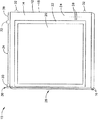
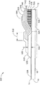
図1は、矩形の検出器基板12を含むデジタルX線パネル10の平面図であり、該基板は検出器ベース面14と、該検出器ベース面14から垂直に延びる少なくとも1つの側壁16と、検出器ベース面14の反対側にある裏面18とを含む。検出器ベース面14は、有効検出器領域20と、ダム領域22と、接触フィンガー領域24と、胸壁側面26と、を含む。
FIG. 1 is a plan view of a
有効検出器領域20は、検出器ベース面14上にある実質的に矩形の領域であり、該検出器ベース面は入射放射線に応答して該入射放射線を電気信号に変換するよう構成され、該電気信号は接触フィンガー領域24上で間隔を置いて配置された複数の接触フィンガー28で受信される。ダム領域22は、有効検出器領域20を取り囲む平坦接着剤コーティングを含む。例示的な実施形態において、パネル10は乳房撮影機器で使用される。従って、ダム領域22の胸壁側部分は幅30を含み、胸壁側面26に隣接しないダム領域22部分は幅32を含む。1つの実施形態において、幅30は0.015インチと0.055インチとの間の範囲にある。別の実施形態において、幅30は0.025インチと0.045インチとの間の範囲にある。例示的な実施形態において、幅30は約0.035インチである。1つの実施形態において、幅32は0.138インチと0.178インチとの間の範囲にある。別の実施形態において、幅32は0.148インチと0.168インチとの間の範囲にある。例示的な実施形態において、幅32は約0.158インチである。厚みの範囲は例証の目的で与えられており、限定を意図するものではない。
The
例示的な実施形態において、幅30の寸法は幅32の寸法よりも小さい。例えば、この構成は、有効検出器領域20ができるだけ患者の胸壁に近いことが望ましい乳房撮影機器においてデジタルX線パネル10が使用される場合に用いることができる。例えばRAD、又は心臓用機器などのような別の実施形態において、幅30の寸法は幅32の寸法以上とすることができる。幅34は有効検出器領域20の幅であり、幅36は胸壁側面26に隣接する基板12の幅であり、幅38は胸壁側面26に隣接しない接触フィンガー領域24の幅である。接触フィンガー28は胸壁側面26側のパネル10には存在しない。1つの実施形態において、幅36は実質的にゼロであり、これは領域30のダム106が基板12の端部まで実質的に延びていることを意味する。
In the exemplary embodiment, the
操作中、患者の一部が、デジタルX線パネル10と放射線すなわちX線源(図示せず)との間に配置される。入射放射線は患者を透過し、該入射放射線の一部は患者に吸収される。患者に吸収されなかった入射放射線の一部は、シンチレータ材料110に実質的に吸収される。シンチレータ材料110はX線信号を光信号に変換し、該光信号は次いで、検出器基板上のフォトダイオードによって電荷に変換される。従って、電気信号は、デジタルX線パネル10が受信した放射線量に比例する。電気信号は接触フィンガー28に示され、さらに解釈電子機器(図示せず)に接続される。
During operation, a portion of the patient is placed between the
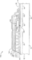
図2は、図1に示されるX線検出器パネルで使用することができる密閉シール構造の断面図である。図2に示す、図1に示された構成要素と同一のものは、図1で使用した同じ符号で示されている。従って、検出器基板12は、検出器ベース面14と、該検出器ベース面14から垂直に延びる側壁16と、検出器ベース面14と反対側にある裏面18とを含む。
FIG. 2 is a cross-sectional view of a hermetic seal structure that can be used with the X-ray detector panel shown in FIG. 2 that are the same as those shown in FIG. 1 are indicated by the same reference numerals used in FIG. Accordingly, the
検出器ベース面14は、有効検出器領域20と、ダム領域22と、接触フィンガー領域24と、接着領域102とを含む。フォトンを検出するために配置されたフォトセンサーのアレイを含む検出器マトリクス104は、有効検出器領域20内の検出器ベース面14上に形成される。検出器マトリクス104の素子は、接触フィンガー28に電気的に接続され、接触フィンガー28との接続の組み合わせにより、検出器マトリクス104の各素子のステータスを決定することができるようにする。平坦接着剤ダム106は、有効検出器領域20の周囲に形成され、検出器マトリクス104に隣接するダム106の第1の側面からダム106の反対側にある第2の面109までの距離である厚さ108を含む。例示的な実施形態において、厚さ108は約0.005インチである。本明細書で述べる、例えば「上に」、「覆って」、及び「上方に」といった用語は、図面に示されたものの相対的位置を言及するものであり、組み立てられた装置の構造的又は操作上の制限を意味するものではない。
The
シンチレータ材料110は、検出器マトリクス104上に形成され、有効検出器領域20を覆う。例示的な実施形態において、シンチレータ材料110は、ヨウ化セシウム(CsI)物質をCsIの針構造111で含む。別の実施形態において、他のシンチレータ材料もまた許容可能である。例示的な実施形態において、CsI針構造111はタリウムがドープされた物質を含む。封入層112は、シンチレータ材料110を覆って形成され、有効検出器領域20、ダム領域22、及び接着領域102の一部を覆って延びる。例示的な実施形態において、封入層112は、シンチレータ針111の各底部まで完全に、及び全シンチレータ針の側壁全体に沿ってシンチレータ針構造111間に堆積される。接着領域102は、封入層112におけるシンチレータ材料110を覆ってシールを形成するための結合領域を形成する。1つの実施形態において封入層112がコーティングしているのは、ポリパラキシリレン材料(パリレン(商標)N)である。別の実施形態において、封入層112がコーティングしているのはモノクロロポリパラキシリレン(パリレン(商標)C)である。別の実施形態において、封入層112がコーティングしているのは、パリレン(商標)C及びパリレン(商標)Nの両方である。パリレン(商標)は、インディアナ州46241インディアナポリス、ウェストミネソタ通り5701所在のSpecialty Coating Systems,Inc.の商標である。
A
反射層114は、例えば、銀、金、二酸化チタン、又はアルミニウムを含み、封入層112を覆って形成され、接着領域102の上方の封入層112の端部まで延びる。例示的な実施形態において、反射層114は、封入層112の端部まで延びる。別の実施形態において、反射層114は、封入層112の端部までではなく、封入層112の端部を超えて延びる。
The
薄膜マスク116は、例えばアルミニウム(Al)、フッ化マグネシウム(MgF)、ダイヤモンド様炭素、炭化ホウ素(B4C)、窒化ホウ素(BNO2)、硝酸ケイ素(SiNO3)、酸化ケイ素(SiO)といった比較的原子量が低い物質を含み、反射層114上に形成される。薄膜マスク116はプラズマエッチングに侵されない。1つの実施形態において、薄膜マスク116は、反応性イオンエッチング(RIE)工程中に反射層114が除去されない場合などは、使用されない。別の実施形態において、薄い障壁層(図示せず)を反射層114と薄膜マスク116との間に形成することができ、これは反射層114が銀を含み、且つ薄膜マスク116がアルミニウムを含む場合などである。このような場合、銀及びアルミニウムは共に拡散する傾向にあり、これらの間の薄い障壁層は、例えばクロムを含み、この拡散の低減を促進する。
The
密閉層118は薄膜マスク116上に形成される。密閉層118もまた、例えばアルミニウム(Al)、フッ化マグネシウム(MgF)、ダイヤモンド様炭素、炭化ホウ素(B4C)、窒化ホウ素(BNO2)、硝酸ケイ素(SiNO3)、酸化ケイ素(SiO)といった比較的原子量が低い物質を含む。密閉層118は、薄膜マスク116上に封入層112に隣接して接着領域102を覆って延びて終端するように形成される。密閉層118及び接着領域102は、水分障壁を与える。腐食保護層120は、密閉層118上に該密閉層118に隣接して接着領域102上で終端するように形成される。腐食保護層120は、例えば、アクリル、パリレン(商標)、アルミニウム(Al)、酸化アルミニウム(AlO)、フッ化マグネシウム(MgF)、ダイヤモンド型炭素、炭化ホウ素(B4C)、窒化ホウ素(BNO2)、硝酸ケイ素(SiNO3)、酸化ケイ素(SiO)、金(Au)といった低X線吸収性の物質を含む。
The
デジタルX線パネル10は、次のようにして作られる。デジタルX線パネル10の有効領域20が、基板12の周囲に配置された多数の接触フィンガー28で製造される。接着材料がダム領域22の検出器基板12上に堆積される。本発明の1つの実施形態において、接着材料はエポキシ材である。本発明の1つの実施形態において、封入コーティング112は、パリレン(商標)N、パリレン(商標)C、及びその組み合わせの少なくとも1つである。
The
エポキシ材料は、Teflon(商標)(デラウェア州19898ウィルミントン、マーケット通り1007所在のthe E.I.du Pont de Nemours and Companyの商標)平坦化取付具(図示せず)を使用して平坦化し、約0.004インチと約0.006インチとの間の範囲にある厚さ108を有する平坦接着ダム106を形成する。厚さ108の範囲は、例証の目的で与えられたものであり、限定を意図するものではない。平坦化取付具は、平坦接着ダム106の硬化後、取り除かれる。合金Kovar(商標)(デラウェア州19810ウィルミントン、シルバーサイドロード3411 Baynardビル209所在のthe CRS Holdings, Inc.の商標)(Ni29%、Fe53%、Co17%、極微量不純物1%)シャドーマスク(図示せず)が、平坦接着ダム106上に布設されて、合金シャドーマスクが接触フィンガー28を覆い、合金Kovar(商標)シャドーマスクの一方端が、接触フィンガー28に最も近接した検出器マトリクス104の周囲を過ぎて延びないようにする。
The epoxy material is flattened using a Teflon ™ (trademark of the EI du Pont de Nemours and Company, Wilmington, Delaware, 1998, Market Street 1007) flattening fixture (not shown), A flat bonded
シンチレータ材料110は、合金シャドーマスクを通って検出器基板12上に堆積され、検出器基板12上の検出器マトリクス104と接触する。シンチレータ材料110が基板12上に堆積する間、接触フィンガー28は、平坦接着ダム106によって、シンチレータ材料110でコーティングされることから保護されるが、該接着ダムは接触フィンガー28とシンチレータ材料110でコートされることになる有効領域20との間の基板12上に堆積される。次いで、接触シャドーマスクが、シンチレータ材料110の堆積中に、ダム106の上部に載置される。シャドーマスクの中央にある窓により、シンチレータ材料110を接触フィンガー28上でなく、有効領域20内にだけ堆積することが可能になる。ダム106とシャドーマスクは、接触フィンガー28がシンチレータ材料110で堆積されることから保護する。
The
合金シャドーマスクが除去される。封入層112がシンチレータ材料110上に堆積され、これはシンチレータ針構造111の間及びこれに沿ったコーティングを含む。封入層112はまた、ダム領域22、接着領域102、平坦接着ダム106、接触フィンガー28上でも堆積される。次いで接触シャドーマスク(図示せず)が、平坦接着ダム106上の封入層112に布設され、接触シャドーマスクが接触フィンガー28を覆い、該接触シャドーマスクの一方端がダム領域22を越えて延びないようにする。反射層114は、封入層112上に堆積され、シンチレータ材料110、平坦接着ダム106、接着領域102を覆う。1つの実施形態において、反射層114は、接着領域102の一部上だけに堆積される。
The alloy shadow mask is removed. An
次に、薄膜マスク116が反射層114上に堆積される。薄膜マスク116は、封入層112が酸素RIEによって除去されときに反射層114を保護する。次いで接触シャドーマスクが取り除かれる。封入層112はRIEにより接触フィンガー28から除去されている。次に密閉層接触シャドーマスク(図示せず)は、シャドーマスクが接触フィンガー28を覆い、且つ密閉層接触シャドーマスクの一方端が接着領域102の一部を覆って延びないように布設される。密閉層118は薄膜マスク116上に堆積され、該密閉層118は薄膜マスク116に隣接して接着領域102で終端し、密閉層118と接着領域102との間に水分障壁を形成するようにする。任意的な腐食保護層120は密閉層118上に堆積され、該腐食保護層120は、密閉層118に隣接して接着領域102で終端する。
Next, a
密閉層118と腐食保護層120は、パネル10の密閉カバーを構成する。任意的な腐食保護層120が使用されない場合には、密閉層118は、容易に腐食せず、密閉層及び腐食保護層の双方の目的を果たす材質から選択される。
The
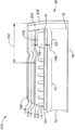
図3は、図1に示されたX線検出器パネル10で使用することができる別の密閉シール構造200の断面図である。図3に示す、図1及び図2に示された構成要素と同一のものは、図1及び2で使用した同じ符号で図3に示されている。従って、検出器基板12は、検出器ベース面14と、該検出器ベース面14から垂直に延びる側壁16と、検出器ベース面14と反対側にある裏面18とを含む。
FIG. 3 is a cross-sectional view of another
密閉シール構造200は、幅202の縮小を促進する。この構造は、例えば乳房撮影機器に使用されるデジタルX線パネル10において有効検出器領域20を胸壁側面26にできる限り近付けることを促進するのに使用される。X線検出器パネル10は、密閉層204及び腐食保護層206が、例えば図3に示されるように右側から密閉層118及び腐食保護層120に対して直角に堆積されることを除いて、構造100と同様にして構造200で作られる。密閉層204は、封入層112、反射層114、薄膜マスク116、密閉層118、及び腐食保護層120の端部と、胸壁側面126の側壁16とを覆って形成される。
The
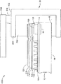
図4は図1に示されたX線検出器パネル10で使用することができる別の密閉シール構造300の断面図である。図4に示す、図1及び図2に示された構成要素と同一のものは、図1及び2で使用した同じ符号で図4に示されている。従って、検出器基板12は、検出器ベース面14と、該検出器ベース面14から垂直に延びる側壁16と、検出器ベース面14の反対側にある裏面18とを含む。
FIG. 4 is a cross-sectional view of another
密閉シール構造300は、図2及び図3にそれぞれ示された密閉シール構造100及び密閉シール構造200と同様に作られる。密閉層118と腐食保護層120に垂直に堆積された密閉層204及び腐食保護層から形成されたシールの代わりに、図4に示す実施形態では、接着シーラント302と末端チャネル304を使用して、デジタルX線パネル10の胸壁側面26を密閉している。例示的な実施形態において、胸壁側面26は、末端チャネル304を使って密閉されたデジタルX線パネル10のただ1つの側面であり、他方の側面は図2に示された実施形態に従って密閉される。
The
接着材料306は、腐食保護層120に対して保護カバー308を支持及び接着するのに十分な量で腐食保護層120に塗布され、保護カバー308と腐食保護層120の間にギャップが残るようにする。例示的な実施形態において、保護カバー308は、アルミ箔で封入された黒鉛/樹脂のコアを含む。腐食保護層120が使用されない別の実施形態においては、接着材料306は密閉層118に塗布される。接着シーラント302は、接着シーラント306及び保護カバー308を含むデジタルX線パネル10の構成要素と末端チャネル304との間の空隙を充填するのに十分な量で胸壁側面26に塗布される。
The
図5は、図1に示されたX線検出器パネル10で使用することができる別の密閉シール構造400の断面図である。図5に示す、図1、図2、図3及び図4に示された構成要素と同一のものは、図1、図2、図3及び図4で使用した同じ符号で図5に示されている。従って、検出器基板12は、検出器ベース面14と、該検出器ベース面14から垂直に延びる側壁16と、検出器ベース面14の反対側にある裏面18とを含む。
FIG. 5 is a cross-sectional view of another
密閉シール構造400は、図4に示された密閉シール構造300と同様に作られる。図4におけるような末端チャネル304内に配置された保護カバー308の代わりに、保護カバー308は図5では末端チャネル304の外面402の外に配置されて示されている。
The
接着シーラント302は、デジタルX線パネル10の構成要素と末端チャネル304との間の空隙を充填するのに十分な量で胸壁側面26に塗布される。接着材料306は、末端チャネル外面402に対して保護カバー308を支持及び接着するのに十分な量で表面402に塗布される。保護カバー308は、腐食保護層が使用されない場合には、腐食保護カバー120又は密閉層118を覆うように配置される。
The
図6は、図1に示されたX線検出器パネル10で使用することができる別の密閉シール構造500の断面図である。密閉シール構造500は、図2に示された密閉シール構造100と同様に作られる。図6に示す、図1に示された構成要素と同一のものは、図1で使用した同じ符号で図6に示されている。従って、検出器基板12は、検出器ベース面14と、検出器ベース面14から垂直に延びる側壁16と、検出器ベース面14の反対側にある裏面18とを含む。
FIG. 6 is a cross-sectional view of another
検出器ベース面14は、有効検出器領域520と、ダム領域522と、接触フィンガー領域524と、領域520とダム領域522との間にあるクリアランス領域525とを備える。フォトンを検出するために配置されたフォトセンサーのアレイを含む検出器マトリクス526は、有効検出器領域520内の検出器ベース面14上に形成される。検出器マトリクス526の素子は、接触フィンガー528に電気的に接続され、該接触フィンガー528との接続の組み合わせにより、検出器マトリクス526の各素子のステータスを決定することができるようにする。平坦接着剤ダム530は、有効検出器領域520の周囲に形成され、検出器マトリクス526に隣接するダム530の第1の側面からダム530の反対側にある第2の面533までの距離である厚さ532を含む。1つの実施形態において、厚さ532は、厚さ0.003インチと0.007インチの間の範囲にある。別の実施形態において、厚さ532は、厚さ0.004インチと0.006インチの間の範囲にある。例示的な実施形態において、厚さ532は約0.005インチである。本明細書で述べる、例えば「上に」、「覆って」、及び「上方に」といった用語は、図面に示されたものの相対的位置を言及するものであり、組み立てられた装置の構造的又は操作上の制限を意味するものではない。
The
シンチレータ材料534は、検出器マトリクス526上に形成され、有効検出器領域520を覆う。例示的な実施形態において、シンチレータ材料534は、ヨウ化セシウム(CsI)をCsI針構造536で含む。別の実施形態において、他のシンチレータ材料もまた許容可能である。例示的な実施形態において、CsI針構造536は、タリウムがドープされた物質を含む。第1封入層542は、シンチレータ材料534を覆って形成され、有効検出器領域520、クリアランス領域525、ダム領域522の一部の距離538を覆って延びる。例示的な実施形態において、封入層542は、シンチレータ針536の各底部まで完全に、及び全シンチレータ針536の側壁全体に沿ってシンチレータ針構造536間に堆積される。1つの実施形態において、封入層542は、厚さが約2.0マイクロメートルと5.0マイクロメートルの間の範囲にある。別の実施形態において、封入層542は、厚さが約2.75マイクロメートルと4.25マイクロメートルの間の範囲にある。例示的な実施形態において、封入層542は、厚さが約3.5マイクロメートルである。厚さの範囲は例証の目的で与えられたものであり、限定を意図するものではない。1つの実施形態において、封入層542はポリパラキシリレン材料(パリレン(商標)N)を含む。別の実施形態において、封入層542はモノクロロポリパラキシリレン材料(パリレン(商標)C)を含む。別の実施形態において、封入層542は、パリレン(商標)C及びパリレン(商標)Nの両方を含む。パリレン(商標)は、インディアナ州46241インディアナポリス、ウェストミネソタ通り5701所在のSpecialty Coating Systems,Inc.の商標である。
A
反射層546は、例えば、銀又は金、二酸化チタン、及びアルミニウムを含み、封入層542を覆って形成され、クリアランス領域525まで延びる。例示的な実施形態において、反射層546は、銀の層、二酸化チタン層、及び厚さ0.5マイクロメートルのアルミニウム層を含む。1つの実施形態において、銀の層は厚さが約1,000オングストロームと2,000オングストロームの間の範囲にある。別の実施形態において、銀の層は厚さが約1,250オングストロームと1,750オングストロームの間の範囲にある。例示的な実施形態において、銀の層は厚さが約1,500オングストロームである。1つの実施形態において、二酸化チタン層は、厚さが約300オングストロームと700オングストロームの間の範囲にある。別の実施形態において、二酸化チタン層は、厚さが約400オングストロームと600オングストロームの間の範囲にある。例示的な実施形態において、二酸化チタン層は、厚さが約500オングストロームである。1つの実施形態において、アルミニウム層は、厚さが約0.3マイクロメートルと0.7マイクロメートルの間の範囲にある。別の実施形態において、アルミニウム層は、厚さが約0.4マイクロメートルと0.6マイクロメートルの間の範囲にある。例示的な実施形態において、アルミニウム層は、厚さが約0.5マイクロメートルである。厚さの範囲は、例証の目的で与えられたものであり、限定を意図するものではない。反射層546の層は、シンチレータ材料534からシンチレータ針536に戻る入射光の反射を促進する大きさにされている。銀及びアルミニウムの層は、共に拡散する傾向にあり、これらの間の薄い障壁層は、例えばチタンを含み、この拡散の低減を促進する。反射層546は、領域520を覆う封入層542を覆い、クリアランス領域525の一部を越えて延びる。
The
第2の封入層548は、反射層546上に形成される。封入層548は、封入層542と実質的に同じであり、パリレン(商標)を同様に含む。層548は層546を覆い、層546の端部を通り、ダム530上の層542の端部まで延びる。1つの実施形態において、封入層548は、厚さが約5マイクロメートルと9マイクロメートルの間の範囲にある。別の実施形態において、封入層548は、厚さが約6マイクロメートルと8マイクロメートルの間の範囲にある。例示的な実施形態において、封入層548は、厚さが約7マイクロメートルである。厚さの範囲は、例証の目的で与えられたものであり、限定を意図するものではない。
The
水分障壁層550は、層548上に堆積されている。例示的な実施形態において、層550は、二酸化チタン層とアルミニウム層とを含む。1つの実施形態において、二酸化チタン層は、厚さが約300オングストロームと700オングストロームの間の範囲にある。別の実施形態において、二酸化チタン層は、厚さが約400オングストロームと600オングストロームの間の範囲にある。例示的な実施形態において、二酸化チタン層は、厚さが約500オングストロームである。1つの実施形態において、アルミニウム層は、厚さが約0.3マイクロメートルと0.7マイクロメートルの間の範囲にある。別の実施形態において、アルミニウム層は、厚さが約0.4マイクロメートルと0.6マイクロメートルの間の範囲にある。例示的な実施形態において、アルミニウム層は、厚さが約0.5マイクロメートルである。例示的な実施形態において、層550は、厚さが約500オングストロームの二酸化チタン層と、厚さが約0.5マイクロメートルのアルミニウム層を含む。厚さの範囲は、例証の目的で与えられたものであり、限定を意図するものではない。層550は層548を覆い、ダム530上の層548の端部まで延びる。
A
任意的な水分障壁層552は、使用される場合には層550上に堆積される。層552は層550を覆い、層550の端部を通ってダム530上へ延びる。1つの実施形態において、層552は、厚さが300オングストロームと700オングストロームの間の範囲にある二酸化チタン層を含む。別の実施形態において、層552は、厚さが400オングストロームと600オングストロームの間の範囲にある。例示的な実施形態において、層552は厚さが約500オングストロームである。厚さの範囲は、例証の目的で与えられたものであり、限定を意図するものではない。
An optional
上述したX線検出器パネルの密閉シールカバーは、例示的な方法で説明されている。密閉カバーの層の数及び順序の違いは、エンドユーザーの状況又は要求に適合するように企図される。 The hermetic seal cover of the X-ray detector panel described above has been described in an exemplary manner. Differences in the number and order of the layers of the hermetic cover are contemplated to suit the end user's circumstances or requirements.
例示的な実施形態において、密閉シール構造500は、末端チャネル304及び保護カバー308では使用されない。別の実施形態において、密閉シール構造500は、図4に示されるように、末端チャネル304及び保護シール308で覆われている。別の実施形態において、密閉シール構造500は、図5に示されるように末端チャネル304及び保護カバー308で覆われている。
In the exemplary embodiment,
上述のデジタルX線パネルにおいて堆積された密閉カバーは、費用効果があり信頼性が高い。堆積された密閉カバーは、複数の堆積層及び複数の密封端部を含む。さらに、任意的な保護カバーが提供され、検出器表面に当たる対象物からの該検出器の損傷を低減することを促進する。その結果、堆積された密閉カバーは、費用効果が高く信頼性のある方法で水分を減少させて検出器構成要素への損傷を低減することを促進する。 The hermetic cover deposited in the digital x-ray panel described above is cost effective and reliable. The deposited hermetic cover includes a plurality of deposited layers and a plurality of sealed edges. In addition, an optional protective cover is provided to help reduce damage to the detector from objects hitting the detector surface. As a result, the deposited hermetic cover facilitates reducing moisture and reducing damage to the detector components in a cost-effective and reliable manner.
堆積された密閉カバーの例示的な実施形態は、上に詳細に説明されている。カバーは本明細書で説明された特定の実施形態に限定されるものではなく、むしろ、カバー構成要素は、本明細書で説明された他の構成要素から独立して別個に使用することができる。堆積された密閉カバー構成要素の各々はまた、他の堆積された密閉カバー構成要素と組み合わせて使用することができる。 Exemplary embodiments of deposited hermetic covers are described in detail above. The cover is not limited to the specific embodiments described herein, but rather the cover component can be used separately and independently of the other components described herein. . Each of the deposited hermetic cover components can also be used in combination with other deposited hermetic cover components.
本発明を様々な特定の実施形態に関して説明してきたが、本発明は請求項の精神及び範囲内にある変更を実施することができることは当業者には認識されるであろう。 While the invention has been described in terms of various specific embodiments, those skilled in the art will recognize that the invention can be practiced with modification within the spirit and scope of the claims.
12 検出器基板
12 検出器ベース面
16 側壁
18 裏面
20 有効検出器領域
22 ダム領域
24 接触フィンガー領域
28 接触フィンガー
100 密閉シール構造
102 接着領域
104 検出器マトリクス
106 ダム
108 厚さ
109 第2の面
110 シンチレータ材料
111 針構造
112 封入コーティング
114 反射層
116 薄膜マスク
118 密閉層
120 腐食保護層
DESCRIPTION OF
Claims (10)
前記検出器基板上に検出器マトリクス526を形成する段階と、
前記検出器マトリクスを取り囲むダム530を前記検出器基板上に形成する段階と、
前記検出器マトリクス上にシンチレータ材料534を形成する段階と、
少なくとも1つが前記ダムの表面に延び且つ該ダムを過ぎて延びる密閉カバーを前記シンチレータ材料上に形成する段階と、
段階を含み、
前記密閉カバーを形成する段階が、
前記シンチレータ材料上に前記ダム表面に延びる第1の封入層542を形成する段階と、
前記第1の封入層上に前記検出器マトリクスと前記ダム表面の間の領域まで延びる反射層546を形成する段階と、
前記反射層546及び前記第1の封入層542上に、前記反射層546の端部を過ぎて前記ダムの表面上の第1の封入層の端部まで延びる第2の封入層548を形成する段階と、
前記第2の封入層548上に前記ダムの表面上の前記第2の封入層548の端部まで延びる第1の水分障壁層550を形成する段階と、
前記第1の水分障壁層550上に前記ダムの表面上の前記第1の水分障壁層550を過ぎて延びる第2の水分障壁層552を形成する段階と、
含む方法。 A method of manufacturing an X-ray detector panel assembly 10 comprising a detector substrate 12, the substrate including a detector base surface 14 and a plurality of sidewalls 16 extending perpendicularly from the detector base surface,
Forming a detector matrix 526 on the detector substrate;
Forming a dam 530 surrounding the detector matrix on the detector substrate;
Forming a scintillator material 534 on the detector matrix;
Forming a hermetic cover on the scintillator material, wherein at least one extends to the surface of the dam and extends past the dam;
Including stages,
Forming the sealing cover comprises:
Forming a first encapsulation layer 542 on the scintillator material extending to the dam surface;
Forming a reflective layer 546 on the first encapsulation layer extending to a region between the detector matrix and the dam surface;
On the reflective layer 546 and the first encapsulating layer 542 , a second encapsulating layer 548 extending past the end of the reflecting layer 546 to the end of the first encapsulating layer on the surface of the dam is formed. Stages,
Forming a first moisture barrier layer 550 on the second encapsulation layer 548 extending to the end of the second encapsulation layer 548 on the surface of the dam;
Forming a second moisture barrier layer 552 extending over the first moisture barrier layer 550 on the surface of the dam on the first moisture barrier layer 550;
Including methods.
前記検出器基板上に形成された検出器マトリクス526と、
前記検出器基板上に形成され、前記検出器マトリクスを取り囲むダム530と、
前記検出器マトリクス上に形成されたシンチレータ材料534と、
前記シンチレータ材料上に形成された密閉カバーと、
を備え、
前記密閉カバーが、
前記シンチレータ材料上に前記ダム表面に延びる第1の封入層542と、
前記第1の封入層上に前記検出器マトリクスと前記ダム表面の間の領域まで延びる反射層546と、
前記反射層546及び前記第1の封入層542上に、前記反射層546の端部を過ぎて前記ダムの表面上の第1の封入層の端部まで延びる第2の封入層548と、
前記第2の封入層548上に前記ダムの表面上の前記第2の封入層548の端部まで延びる第1の水分障壁層550と、
前記第1の水分障壁層550上に前記ダムの表面上の前記第1の水分障壁層550を過ぎて延びる第2の水分障壁層552と、
含むことを特徴とするデジタルX線パネル10。 A detector substrate 12;
A detector matrix 526 formed on the detector substrate;
A dam 530 formed on the detector substrate and surrounding the detector matrix;
A scintillator material 534 formed on the detector matrix;
A hermetic cover formed on the scintillator material;
With
The sealing cover is
A first encapsulating layer 542 extending to the dam surface on the scintillator material;
A reflective layer 546 extending on the first encapsulation layer to a region between the detector matrix and the dam surface;
A second encapsulation layer 548 extending over the reflective layer 546 and the first encapsulation layer 542 past the end of the reflective layer 546 to the end of the first encapsulation layer on the surface of the dam;
A first moisture barrier layer 550 extending on the second encapsulation layer 548 to the end of the second encapsulation layer 548 on the surface of the dam;
A second moisture barrier layer 552 extending over the first moisture barrier layer 550 over the first moisture barrier layer 550 on the surface of the dam;
A digital X-ray panel 10 comprising:
Applications Claiming Priority (1)
| Application Number | Priority Date | Filing Date | Title |
|---|---|---|---|
| US10/365,093 US7473903B2 (en) | 2003-02-12 | 2003-02-12 | Method and apparatus for deposited hermetic cover for digital X-ray panel |
Publications (3)
| Publication Number | Publication Date |
|---|---|
| JP2004245833A JP2004245833A (en) | 2004-09-02 |
| JP2004245833A5 JP2004245833A5 (en) | 2007-03-22 |
| JP4445281B2 true JP4445281B2 (en) | 2010-04-07 |
Family
ID=32736392
Family Applications (1)
| Application Number | Title | Priority Date | Filing Date |
|---|---|---|---|
| JP2004033028A Expired - Fee Related JP4445281B2 (en) | 2003-02-12 | 2004-02-10 | Method for manufacturing X-ray detector panel assembly and digital X-ray panel |
Country Status (4)
| Country | Link |
|---|---|
| US (1) | US7473903B2 (en) |
| JP (1) | JP4445281B2 (en) |
| DE (1) | DE102004005883A1 (en) |
| FR (1) | FR2851051A1 (en) |
Cited By (1)
| Publication number | Priority date | Publication date | Assignee | Title |
|---|---|---|---|---|
| KR20170138403A (en) | 2015-04-20 | 2017-12-15 | 하마마츠 포토닉스 가부시키가이샤 | Radiation detector and manufacturing method thereof |
Families Citing this family (17)
| Publication number | Priority date | Publication date | Assignee | Title |
|---|---|---|---|---|
| US7492019B2 (en) * | 2003-03-07 | 2009-02-17 | Ic Mechanics, Inc. | Micromachined assembly with a multi-layer cap defining a cavity |
| DE102005055176A1 (en) * | 2005-11-18 | 2007-05-31 | Siemens Ag | Flat screen detector for digital x-ray imaging, has housing with radiation entrance window that is dazzled through foil or foil like material, which is x-ray permeable and absorbs five percent of impinging x-rays |
| JP2007149842A (en) * | 2005-11-25 | 2007-06-14 | Sanyo Electric Co Ltd | Semiconductor device |
| DE102006022138A1 (en) * | 2006-05-11 | 2007-11-15 | Siemens Ag | scintillator |
| DE102006024893A1 (en) * | 2006-05-24 | 2007-12-06 | Siemens Ag | scintillator |
| DE102006038969B4 (en) * | 2006-08-21 | 2013-02-28 | Siemens Aktiengesellschaft | X-ray converter element and method for its production |
| JP5883556B2 (en) * | 2010-06-04 | 2016-03-15 | 浜松ホトニクス株式会社 | Radiation image sensor |
| JP2012168128A (en) * | 2011-02-16 | 2012-09-06 | Canon Inc | Radiation detection device and radiation imaging system |
| US8415628B1 (en) | 2011-10-31 | 2013-04-09 | General Electric Company | Hermetically sealed radiation detector and methods for making |
| EP3004930B1 (en) * | 2013-05-24 | 2019-07-10 | Teledyne Dalsa B.V. | A moisture protection structure for a device and a fabrication method thereof |
| US10712454B2 (en) * | 2014-07-25 | 2020-07-14 | General Electric Company | X-ray detectors supported on a substrate having a metal barrier |
| CA2968415C (en) | 2014-11-21 | 2020-10-27 | Anton Petrus Maria Van Arendonk | Mammography detector with small chest distance |
| US10299744B2 (en) | 2016-11-17 | 2019-05-28 | General Electric Company | Scintillator sealing for solid state x-ray detector |
| US10631801B2 (en) | 2016-11-17 | 2020-04-28 | General Electric Company | Scintillator sealing for solid state X-ray detector |
| US9871073B1 (en) | 2016-11-22 | 2018-01-16 | General Electric Company | Scintillator sealing for solid state X-ray detector |
| US9812510B1 (en) | 2016-12-14 | 2017-11-07 | General Electric Company | Packaging organic photodetectors |
| JP6877289B2 (en) * | 2017-07-31 | 2021-05-26 | キヤノン株式会社 | Manufacturing method of radiation detection device, radiation detection system, and radiation emission device |
Family Cites Families (19)
| Publication number | Priority date | Publication date | Assignee | Title |
|---|---|---|---|---|
| US5187369A (en) | 1990-10-01 | 1993-02-16 | General Electric Company | High sensitivity, high resolution, solid state x-ray imaging device with barrier layer |
| US5179284A (en) * | 1991-08-21 | 1993-01-12 | General Electric Company | Solid state radiation imager having a reflective and protective coating |
| US5231654A (en) | 1991-12-06 | 1993-07-27 | General Electric Company | Radiation imager collimator |
| US5231655A (en) | 1991-12-06 | 1993-07-27 | General Electric Company | X-ray collimator |
| US5463225A (en) | 1992-06-01 | 1995-10-31 | General Electric Company | Solid state radiation imager with high integrity barrier layer and method of fabricating |
| US5399884A (en) | 1993-11-10 | 1995-03-21 | General Electric Company | Radiation imager with single passivation dielectric for transistor and diode |
| US5435608A (en) | 1994-06-17 | 1995-07-25 | General Electric Company | Radiation imager with common passivation dielectric for gate electrode and photosensor |
| US5517031A (en) | 1994-06-21 | 1996-05-14 | General Electric Company | Solid state imager with opaque layer |
| US5430298A (en) | 1994-06-21 | 1995-07-04 | General Electric Company | CT array with improved photosensor linearity and reduced crosstalk |
| US6037609A (en) | 1997-01-17 | 2000-03-14 | General Electric Company | Corrosion resistant imager |
| US6167110A (en) | 1997-11-03 | 2000-12-26 | General Electric Company | High voltage x-ray and conventional radiography imaging apparatus and method |
| DE69833502T2 (en) * | 1998-05-15 | 2006-09-28 | The Board Of Trustees Of The Leland Stanford Junior University, Palo Alto | GLUCOCORTICOID RECEPTOR ANTAGONISTS FOR THE TREATMENT OF DEMENTIA |
| US6172371B1 (en) * | 1998-06-15 | 2001-01-09 | General Electric Company | Robust cover plate for radiation imager |
| US6414315B1 (en) | 1999-10-04 | 2002-07-02 | General Electric Company | Radiation imaging with continuous polymer layer for scintillator |
| US6396046B1 (en) | 1999-11-02 | 2002-05-28 | General Electric Company | Imager with reduced FET photoresponse and high integrity contact via |
| US6350990B1 (en) * | 1999-11-04 | 2002-02-26 | General Electric Company | End cap and sealing method for imager |
| US6353654B1 (en) | 1999-12-30 | 2002-03-05 | General Electric Company | Method and apparatus for compensating for image retention in an amorphous silicon imaging detector |
| JP4234304B2 (en) * | 2000-05-19 | 2009-03-04 | 浜松ホトニクス株式会社 | Radiation detector |
| US6642524B2 (en) * | 2002-01-09 | 2003-11-04 | Ge Medical Systems Global Technology Company, Llc | Scintillator sealing for solid state X-ray detector |
-
2003
- 2003-02-12 US US10/365,093 patent/US7473903B2/en not_active Expired - Fee Related
-
2004
- 2004-02-05 DE DE102004005883A patent/DE102004005883A1/en not_active Withdrawn
- 2004-02-10 JP JP2004033028A patent/JP4445281B2/en not_active Expired - Fee Related
- 2004-02-11 FR FR0401326A patent/FR2851051A1/en not_active Withdrawn
Cited By (2)
| Publication number | Priority date | Publication date | Assignee | Title |
|---|---|---|---|---|
| KR20170138403A (en) | 2015-04-20 | 2017-12-15 | 하마마츠 포토닉스 가부시키가이샤 | Radiation detector and manufacturing method thereof |
| US10379229B2 (en) | 2015-04-20 | 2019-08-13 | Hamamatsu Photonics K.K. | Radiation detector and method for producing same |
Also Published As
| Publication number | Publication date |
|---|---|
| JP2004245833A (en) | 2004-09-02 |
| DE102004005883A1 (en) | 2004-08-26 |
| US20040155320A1 (en) | 2004-08-12 |
| US7473903B2 (en) | 2009-01-06 |
| FR2851051A1 (en) | 2004-08-13 |
Similar Documents
| Publication | Publication Date | Title |
|---|---|---|
| JP4445281B2 (en) | Method for manufacturing X-ray detector panel assembly and digital X-ray panel | |
| JP3077941B2 (en) | Radiation detecting element and method of manufacturing the same | |
| JP3126715B2 (en) | Scintillator panel and radiation image sensor | |
| US7408177B2 (en) | Scintillator panel and radiation image sensor | |
| JP3405706B2 (en) | Radiation detection element | |
| JP4317921B2 (en) | X-ray detector assembly | |
| EP1134596A2 (en) | Radiation detection device and method of making the same | |
| US7126130B2 (en) | Direct scintillator coating for radiation detector assembly longevity | |
| KR20010052994A (en) | Radiation image sensor | |
| US20110147602A1 (en) | Radiographic imaging apparatus, radiographic imaging system, and method of producing radiographic imaging apparatus | |
| JP4099206B2 (en) | Scintillator panel and radiation image sensor | |
| US6940072B2 (en) | Radiation detection device and method of making the same | |
| EP1300693B1 (en) | Radiation detector and method of producing the same | |
| TWI591368B (en) | Radiation detector and manufacturing method thereof | |
| JP3987438B2 (en) | Scintillator panel and radiation image sensor | |
| EP1300694B1 (en) | Radiation detector and method of manufacture thereof | |
| EP1503419B1 (en) | Dual para-xylylene layers for an x-ray detector | |
| JP2004301516A (en) | Radiation detection apparatus | |
| JP4283863B2 (en) | Scintillator panel | |
| JP2014059246A (en) | Radiation detector and method for manufacturing the same | |
| JP4234305B2 (en) | Radiation detector | |
| JP2007205935A (en) | Radiation detector | |
| WO2019097847A1 (en) | Radiation imaging panel, radiation imaging device, and radiation imaging system | |
| EP4325255A1 (en) | Manufacturing method of a radiation imaging apparatus |
Legal Events
| Date | Code | Title | Description |
|---|---|---|---|
| A521 | Request for written amendment filed |
Free format text: JAPANESE INTERMEDIATE CODE: A523 Effective date: 20070206 |
|
| A621 | Written request for application examination |
Free format text: JAPANESE INTERMEDIATE CODE: A621 Effective date: 20070206 |
|
| A131 | Notification of reasons for refusal |
Free format text: JAPANESE INTERMEDIATE CODE: A131 Effective date: 20081202 |
|
| A601 | Written request for extension of time |
Free format text: JAPANESE INTERMEDIATE CODE: A601 Effective date: 20090224 |
|
| A602 | Written permission of extension of time |
Free format text: JAPANESE INTERMEDIATE CODE: A602 Effective date: 20090227 |
|
| A521 | Request for written amendment filed |
Free format text: JAPANESE INTERMEDIATE CODE: A523 Effective date: 20090402 |
|
| RD02 | Notification of acceptance of power of attorney |
Free format text: JAPANESE INTERMEDIATE CODE: A7422 Effective date: 20090402 |
|
| RD04 | Notification of resignation of power of attorney |
Free format text: JAPANESE INTERMEDIATE CODE: A7424 Effective date: 20090402 |
|
| A02 | Decision of refusal |
Free format text: JAPANESE INTERMEDIATE CODE: A02 Effective date: 20090512 |
|
| A521 | Request for written amendment filed |
Free format text: JAPANESE INTERMEDIATE CODE: A523 Effective date: 20090810 |
|
| A911 | Transfer to examiner for re-examination before appeal (zenchi) |
Free format text: JAPANESE INTERMEDIATE CODE: A911 Effective date: 20090928 |
|
| TRDD | Decision of grant or rejection written | ||
| A01 | Written decision to grant a patent or to grant a registration (utility model) |
Free format text: JAPANESE INTERMEDIATE CODE: A01 Effective date: 20091222 |
|
| A01 | Written decision to grant a patent or to grant a registration (utility model) |
Free format text: JAPANESE INTERMEDIATE CODE: A01 |
|
| A61 | First payment of annual fees (during grant procedure) |
Free format text: JAPANESE INTERMEDIATE CODE: A61 Effective date: 20100115 |
|
| R150 | Certificate of patent or registration of utility model |
Free format text: JAPANESE INTERMEDIATE CODE: R150 |
|
| FPAY | Renewal fee payment (event date is renewal date of database) |
Free format text: PAYMENT UNTIL: 20130122 Year of fee payment: 3 |
|
| R250 | Receipt of annual fees |
Free format text: JAPANESE INTERMEDIATE CODE: R250 |
|
| LAPS | Cancellation because of no payment of annual fees |