JP4431402B2 - Plasma etching method - Google Patents
Plasma etching method Download PDFInfo
- Publication number
- JP4431402B2 JP4431402B2 JP2003582803A JP2003582803A JP4431402B2 JP 4431402 B2 JP4431402 B2 JP 4431402B2 JP 2003582803 A JP2003582803 A JP 2003582803A JP 2003582803 A JP2003582803 A JP 2003582803A JP 4431402 B2 JP4431402 B2 JP 4431402B2
- Authority
- JP
- Japan
- Prior art keywords
- plasma
- chamber
- etching
- electrodes
- substrate
- Prior art date
- Legal status (The legal status is an assumption and is not a legal conclusion. Google has not performed a legal analysis and makes no representation as to the accuracy of the status listed.)
- Expired - Lifetime
Links
Images


Classifications
-
- H—ELECTRICITY
- H01—ELECTRIC ELEMENTS
- H01J—ELECTRIC DISCHARGE TUBES OR DISCHARGE LAMPS
- H01J37/00—Discharge tubes with provision for introducing objects or material to be exposed to the discharge, e.g. for the purpose of examination or processing thereof
- H01J37/32—Gas-filled discharge tubes
- H01J37/32431—Constructional details of the reactor
- H01J37/3266—Magnetic control means
- H01J37/32688—Multi-cusp fields
-
- H—ELECTRICITY
- H01—ELECTRIC ELEMENTS
- H01L—SEMICONDUCTOR DEVICES NOT COVERED BY CLASS H10
- H01L21/00—Processes or apparatus adapted for the manufacture or treatment of semiconductor or solid state devices or of parts thereof
- H01L21/02—Manufacture or treatment of semiconductor devices or of parts thereof
- H01L21/04—Manufacture or treatment of semiconductor devices or of parts thereof the devices having at least one potential-jump barrier or surface barrier, e.g. PN junction, depletion layer or carrier concentration layer
- H01L21/18—Manufacture or treatment of semiconductor devices or of parts thereof the devices having at least one potential-jump barrier or surface barrier, e.g. PN junction, depletion layer or carrier concentration layer the devices having semiconductor bodies comprising elements of Group IV of the Periodic System or AIIIBV compounds with or without impurities, e.g. doping materials
- H01L21/30—Treatment of semiconductor bodies using processes or apparatus not provided for in groups H01L21/20 - H01L21/26
- H01L21/31—Treatment of semiconductor bodies using processes or apparatus not provided for in groups H01L21/20 - H01L21/26 to form insulating layers thereon, e.g. for masking or by using photolithographic techniques; After treatment of these layers; Selection of materials for these layers
- H01L21/3105—After-treatment
- H01L21/311—Etching the insulating layers by chemical or physical means
- H01L21/31127—Etching organic layers
- H01L21/31133—Etching organic layers by chemical means
- H01L21/31138—Etching organic layers by chemical means by dry-etching
-
- H—ELECTRICITY
- H01—ELECTRIC ELEMENTS
- H01L—SEMICONDUCTOR DEVICES NOT COVERED BY CLASS H10
- H01L21/00—Processes or apparatus adapted for the manufacture or treatment of semiconductor or solid state devices or of parts thereof
- H01L21/02—Manufacture or treatment of semiconductor devices or of parts thereof
- H01L21/04—Manufacture or treatment of semiconductor devices or of parts thereof the devices having at least one potential-jump barrier or surface barrier, e.g. PN junction, depletion layer or carrier concentration layer
- H01L21/18—Manufacture or treatment of semiconductor devices or of parts thereof the devices having at least one potential-jump barrier or surface barrier, e.g. PN junction, depletion layer or carrier concentration layer the devices having semiconductor bodies comprising elements of Group IV of the Periodic System or AIIIBV compounds with or without impurities, e.g. doping materials
- H01L21/30—Treatment of semiconductor bodies using processes or apparatus not provided for in groups H01L21/20 - H01L21/26
- H01L21/31—Treatment of semiconductor bodies using processes or apparatus not provided for in groups H01L21/20 - H01L21/26 to form insulating layers thereon, e.g. for masking or by using photolithographic techniques; After treatment of these layers; Selection of materials for these layers
- H01L21/3105—After-treatment
- H01L21/311—Etching the insulating layers by chemical or physical means
- H01L21/31144—Etching the insulating layers by chemical or physical means using masks
-
- H—ELECTRICITY
- H01—ELECTRIC ELEMENTS
- H01J—ELECTRIC DISCHARGE TUBES OR DISCHARGE LAMPS
- H01J2237/00—Discharge tubes exposing object to beam, e.g. for analysis treatment, etching, imaging
- H01J2237/32—Processing objects by plasma generation
- H01J2237/33—Processing objects by plasma generation characterised by the type of processing
- H01J2237/334—Etching
- H01J2237/3343—Problems associated with etching
- H01J2237/3347—Problems associated with etching bottom of holes or trenches
Landscapes
- Engineering & Computer Science (AREA)
- Physics & Mathematics (AREA)
- Microelectronics & Electronic Packaging (AREA)
- General Physics & Mathematics (AREA)
- Manufacturing & Machinery (AREA)
- Computer Hardware Design (AREA)
- Condensed Matter Physics & Semiconductors (AREA)
- Power Engineering (AREA)
- Chemical & Material Sciences (AREA)
- Chemical Kinetics & Catalysis (AREA)
- General Chemical & Material Sciences (AREA)
- Plasma & Fusion (AREA)
- Analytical Chemistry (AREA)
- Drying Of Semiconductors (AREA)
- Plasma Technology (AREA)
Description
技 術 分 野
本発明は、半導体ウエハ等の被処理基板に形成された低誘電率膜(low−k膜)等の有機系材料膜を、当該膜の途中までプラズマエッチングするプラズマエッチング方法に関する。
背 景 技 術
半導体デバイスの配線形成工程では、配線層を導通させるために配線層間に形成された層間絶縁膜がエッチングされる。層間絶縁膜としては、近時、半導体デバイスのさらなる高速化を実現するために、より低誘電率の膜が求められている。そして、そのような低誘電率の膜として、有機系材料膜が用いられつつある。
有機系材料膜のエッチングは、プラズマエッチングにより行われている。具体的には、チャンバー内に上下に対向する一対の対向電極を設け、下部電極に半導体ウエハ(以下、単にウエハと記載する)を載置して、当該下部電極に13.56〜40MHz程度の高周波電力を供給して、エッチングが行われている。
しかしながら、有機系材料膜に対するトレンチエッチングにおいて、例えばストップレイヤーなしのシングルダマシン構造あるいはデュアルダマシン構造のように、膜の途中でエッチングを停止してエッチングにより形成された溝の底部を平坦部とする場合には、当該溝の底部のエッジ部分にマイクロトレンチングが発生するという問題がある。マイクロトレンチングが発生すると、その後の埋め込み層形成の際に、埋め込み不良が生じたり電荷の集中が生じるといった不都合がある。
発明の要旨
本発明はかかる事情に鑑みてなされたものであって、有機系材料膜をその膜の途中まで平坦な底部を有する溝が形成されるようにプラズマエッチングする際に、マイクロトレンチングの発生を抑制することができるプラズマエッチング方法を提供することを目的とする。
本発明者らの検討結果によれば、有機系材料膜のエッチングでは、プラズマ密度が支配的であって、イオンエネルギーの寄与が小さいことが判明している。一方、マイクロトレンチングは、イオンの垂直方向のエネルギーが大きいと発生する。したがって、マイクロトレンチングを抑制して、かつ、有機系材料膜を高エッチングレートでエッチングするためには、プラズマ密度が高く、かつ、イオンエネルギーがある程度低いことが必要である。この場合、プラズマのイオンエネルギーは、エッチングの際における電極の自己バイアス電圧と間接的に対応する。従って、マイクロトレンチングを抑制しつつ有機系材料膜を高エッチングレートでエッチングするためには、結局、高プラズマ密度かつ低バイアスの条件でエッチングすることが必要である。本発明者らのさらなる検討結果によれば、電極に印加する高周波電力の周波数が高ければ、よりプラズマ密度が高くかつ自己バイアス電圧が小さい状態を実現することができることが判明した。
本発明は、チャンバー内に一対の電極を対向して配置し、両電極の間に有機系材料膜を有する被処理基板が配置されるように、一方の電極によって当該被処理基板を支持させる配置工程と、少なくとも一方の電極に高周波電力を印加して前記一対の電極間に高周波電界を形成するとともに、チャンバー内に処理ガスを供給し、前記電界により処理ガスのプラズマを形成し、該プラズマにより前記被処理基板の前記有機系材料膜を当該膜の途中まで平坦な底部を有する溝が形成されるようにプラズマエッチングするエッチング工程と、を備え、前記エッチング工程において、前記少なくとも一方の電極に印加する高周波電力の周波数が、50〜150MHzであることを特徴とするプラズマエッチング方法である。
本発明によれば、電極に印加される高周波電力の周波数が50〜150MHzであって従来よりも高いため、高密度のプラズマでありながら、低い自己バイアス電圧を実現することができる。これにより、マイクロトレンチングを抑制しつつ、有機系材料膜を高エッチングレートでエッチングすることができる。
好ましくは、前記エッチング工程において、前記チャンバー内の圧力は1.33〜13.3Paである。
また、好ましくは、前記エッチング工程において、前記チャンバー内のプラズマ密度は5×10¹⁰〜1×1011cm−3である。
また、前記高周波電力は、前記被処理基板を支持する電極に印加されることが好ましい。この場合に、被処理基板を支持する電極に、前記高周波電力に重畳させて500kHz〜27MHzの第2高周波電力が印加されてもよい。このように、より低い周波数の第2高周波電力を重畳させることにより、エッチングレートをより上昇させることが可能である。
しかし一方で、第2高周波電力を重畳させると、そのイオン引き込み効果によって、マイクロトレンチングがより発生し易くなる。これに対しては、前記チャンバー内の圧力を53Pa以上の高い値とすることで対応できる。このようにチャンバー内の圧力を高くすることにより、イオン同士が衝突して散乱するので、マイクロトレンチングを有効に抑制することができる。
勿論、第2高周波電力を重畳させない場合にも、チャンバー内圧力を53Pa以上の高い値に設定することにより、より有効にマイクロトレンチングを抑制することができる。ただし、チャンバー内の圧力が133Paを越えるとCDシフトが大きくなる。従って、チャンバー内の圧力は53〜133Paが好ましい。
また、第2高周波電力を重畳させるには、電極の自己バイアス電圧が600V以下であることが好ましい。
また、前記エッチング工程において、前記チャンバー内の処理ガスの滞在時間は、70〜180msecであることが好ましい。
あるいは、被処理基板の面積に電極間距離を掛けて求めた有効チャンバー体積をV(m3)とし、排気速度をS(m3/sec)とした場合に、V/Sの値が70〜180msecであることが好ましい。
また、本発明は、チャンバー内に一対の電極を対向して配置し、両電極の間に有機系材料膜を有する被処理基板が配置されるように、一方の電極によって当該被処理基板を支持させる配置工程と、少なくとも一方の電極に高周波電力を印加して前記一対の電極間に高周波電界を形成するとともに、チャンバー内に処理ガスを供給し、前記電界により処理ガスのプラズマを形成し、該プラズマにより前記被処理基板の前記有機系材料膜を当該膜の途中まで平坦な底部を有する溝が形成されるようにプラズマエッチングするエッチング工程と、を備え、前記エッチング工程において、前記チャンバー内の圧力が1.33〜13.3Paであり、前記チャンバー内のプラズマ密度が5×10¹⁰〜1×1011cm−3であって、かつ、電極の自己バイアス電圧が300V以下であることを特徴とするプラズマエッチング方法である。
本発明によれば、前記チャンバー内の圧力が1.33〜13.3Paであり、前記チャンバー内のプラズマ密度が5×10¹⁰〜1×1011cm−3であって、かつ、電極の自己バイアス電圧が300V以下であるという条件でプラズマが形成されるため、マイクロトレンチングを抑制しつつ、有機系材料膜を高エッチングレートでエッチングすることができる。
また、本発明は、チャンバー内に一対の電極を対向して配置し、両電極の間に有機系材料膜を有する被処理基板が配置されるように、一方の電極によって当該被処理基板を支持させる配置工程と、少なくとも一方の電極に高周波電力を印加して前記一対の電極間に高周波電界を形成するとともに、チャンバー内に処理ガスを供給し、前記電界により処理ガスのプラズマを形成し、該プラズマにより前記被処理基板の前記有機系材料膜を当該膜の途中まで平坦な底部を有する溝が形成されるようにプラズマエッチングするエッチング工程と、を備え、前記エッチング工程において、前記チャンバー内の圧力が53〜133Paであり、前記チャンバー内のプラズマ密度が1×10¹¹〜2×1011cm−3であって、かつ、電極の自己バイアス電圧が600V以下であることを特徴とするプラズマエッチング方法である。
本発明によれば、前記チャンバー内の圧力が53〜133Paであり、前記チャンバー内のプラズマ密度が1×10¹¹〜2×1011cm−3であって、かつ、電極の自己バイアス電圧が600V以下であるという条件でプラズマが形成されるため、マイクロトレンチングを抑制しつつ、有機系材料膜を高エッチングレートでエッチングすることができる。
以上において、前記処理ガスは、例えば、N2ガス、H2ガス、O2ガス、COガス、NH3ガス、CxHyで表されるガス(x、yは自然数)、及び、希ガスの中から選択された少なくとも1種である。
また、前記有機系材料膜は、O、C、及び、Hを含み得る。あるいは、前記有機系材料膜は、Si、O、C、及び、Hを含み得る。典型的には、前記有機系材料膜は、低誘電率膜(low−k膜)である。
なお、マイクロトレンチングは、溝幅が広いほど発生し易い。従って、本発明は、前記平坦部の幅が0.5μm以上である場合に特に有効である。
ところで、パッシェンの法則(Paschen’s law)より、放電開始電圧Vsは、ガス圧力pと電極間距離dの積pdがある値の時に極小値(パッシェン最小値)をとり、パッシェン最小値をとる積pdの値は、高周波電力の周波数が大きいほど小さくなる。従って、高周波電力の周波数が大きい場合に、放電開始電圧Vsを小さくして放電を容易にして安定させるためには、ガス圧力pが一定であれば電極間距離dを小さくする必要がある。そのため、本発明では、電極間距離を50mm未満とすることが好ましい。また、電極間距離を50mm未満とすることで、チャンバー内でのガスのレジデンスタイムを短くすることができる。これにより、反応生成物が効率的に排出され、エッチングストップを低減することができるという効果も得られる。
発明を実施するための最良の形態
以下、添付図面を参照して本発明の実施の形態について説明する。
図1は、本発明の実施に用いられるプラズマエッチング装置を示す断面図である。このエッチング装置は、気密に構成され、小径の上部1aと大径の下部1bとからなる段つき円筒状のチャンバー1を備えている。チャンバー1の壁部は、例えばアルミニウム製である。
チャンバー1内には、被処理基板であるウエハWを水平に支持する支持テーブル2が設けられている。支持テーブル2は例えばアルミニウムで構成され、絶縁板3を介して導体の支持台4上に支持されている。また、支持テーブル2の上方の外周には、導電性材料または絶縁性材料で形成されたフォーカスリング5が設けられている。ウエハWの直径が200mmφの場合、フォーカスリング5は240〜280mmφであることが好ましい。支持テーブル2、絶縁板3、支持台4及びフォーカスリング5は、ボールねじ7を含むボールねじ機構により昇降可能となっている。支持台4の下方の昇降駆動部分は、ステンレス鋼(SUS)製のベローズ8で覆われている。チャンバー1は接地されている。また、支持テーブル2の中には冷媒流路(図示せず)が設けられて支持テーブル2を冷却可能となっている。また、ベローズ8の外側にはベローズカバー9が設けられている。
支持テーブル2のほぼ中央には、高周波電力を供給するための給電線12が接続されている。この給電線12には、マッチングボックス11を介して高周波電源10が接続されている。高周波電源10からは、所定の周波数の高周波電力が支持テーブル2に供給されるようになっている。一方、支持テーブル2の上方には、後述するシャワーヘッド16が互いに平行に対向するように設けられている。シャワーヘッド16は、接地されている。したがって、支持テーブル2は下部電極として機能し、シャワーヘッド16は上部電極として機能して、すなわち、支持テーブル2とシャワーヘッド16とは一対の平板電極を構成している。
なお、これらの電極間の距離は、50mm未満に設定されることが好ましい。その理由は以下のとおりである。
パッシェンの法則(Paschen’s law)により、放電開始電圧Vsは、ガス圧力pと電極間距離dの積pdがある値の時に極小値(パッシェン最小値)をとり、パッシェン最小値をとる積pdの値は、高周波電力の周波数が大きいほど小さくなる。従って、本実施形態のように高周波電力の周波数が大きい場合に、放電開始電圧Vsを小さくして放電を容易にして安定させるためには、ガス圧力pが一定であれば電極間距離dを小さくする必要がある。そのため、電極間距離を50mm未満とすることが好ましい。また、電極間距離を50mm未満とすることで、チャンバー内でのガスのレジデンスタイムを短くすることができる。これにより、反応生成物が効率的に排出され、エッチングストップを低減することができるという効果も得られる。
しかし、電極間距離を小さくしすぎると、被処理基板であるウエハWの表面の圧力分布(中心部と周辺部の圧力差)が大きくなる。この場合、エッチング均一性の低下等の問題が生じ得る。ガス流量によらず、圧力差を0.27Pa(2mTorr)より小さくするためには、電極間距離は35mm以上であることが好ましい。
支持テーブル2の表面上には、ウエハWを静電吸着するための静電チャック6が設けられている。この静電チャック6は、絶縁体6bの間に電極6aが介在されて構成されている。電極6aには直流電源13が接続されている。そして、電極6aに直流電源13から電圧が印加されることにより、例えばクーロン力によって半導体ウエハWが吸着されるようになっている。
支持テーブル2の内部には、図示しない冷媒流路が形成されている。その中に適宜の冷媒を循環させることによって、ウエハWを所定の温度に制御可能となっている。また、冷媒からの冷熱を効率よくウエハWに伝達するために、ウエハWの裏面にHeガスを供給するガス導入機構(図示せず)が設けられている。さらに、フォーカスリング5の外側にはバッフル板14が設けられている。バッフル板14は、支持台4及びベローズ8を通して、チャンバー1と導通している。
チャンバー1の天井壁部分には、支持テーブル2に対向するようにシャワーヘッド16が設けられている。シャワーヘッド16は、その下面に多数のガス吐出孔18が設けられており、かつその上部にガス導入部16aを有している。そして、その内部には空間17が形成されている。ガス導入部16aにはガス供給配管15aが接続されており、このガス供給配管15aの他端には、エッチング処理を行うための処理ガスを供給する処理ガス供給系15が接続されている。この処理ガスとしては、通常この分野で使用されるものを適用することができ、N2ガス、H2ガス、O2ガス、COガス、NH3ガス、CxHy(ただし、x、yは自然数である)で表されるガス、及び、希ガス、の中から選択された少なくとも1種を用いることができる。
このような処理ガスが、処理ガス供給系15からガス供給配管15a及びガス導入部16aを介してシャワーヘッド16の空間17に至り、ガス吐出孔18から吐出され、ウエハWに形成された膜がエッチングされる。
チャンバー1の下部1bの側壁には、排気ポート19が形成されており、この排気ポート19には真空ポンプを有する排気系20が接続されている。そして真空ポンプを作動させることにより、チャンバー1内は所定の真空度まで減圧され得るようになっている。一方、処理室1の下部1bの側壁上側には、ウエハWの搬入出口と、当該搬入出口を開閉するゲートバルブ24と、が設けられている。
一方、チャンバー1の上部1aの周囲には、同心状に、リング磁石21が配置されており、支持テーブル2とシャワーヘッド16との間の処理空間の周囲に磁界を形成するようになっている。このリング磁石21は、回転機構25により配置の中心軸周りに(周方向に)回転可能となっている。
リング磁石21は、図2の水平断面図に示すように、永久磁石からなる複数のセグメント磁石22が図示しない支持部材により支持された状態でリング状に配置されて構成されている。この例では、16個のセグメント磁石22がリング状(同心円状)にマルチポール状態で配置されている。すなわち、リング磁石21においては、隣接するセグメント磁石22同士の磁極の向きが互いに逆向きになるように配置されている。したがって、磁力線は図示のように隣接するセグメント磁石22間に形成され、処理空間の周辺部のみに例えば0.02〜0.2T(200〜2000Gauss)、好ましくは0.03〜0.045T(300〜450Gauss)の磁場が形成される。一方、ウエハ配置領域は、実質的に無磁場状態となる。前記のような磁場強度が規定されるのは、磁場が強すぎると洩れ磁場の原因となり得るし、磁場が弱すぎるとプラズマ閉じこめ効果が得られなくなるためである。もっとも、適正な磁場強度は、装置構造等にも依存する。すなわち、適正な磁場強度の範囲は、装置によって異なり得る。
また、処理空間の周辺部に前記のような磁場が形成される場合、フォーカスリング5上の磁場強度は0.001T(10Gauss)以上となることが望ましい。この場合、フォーカスリング上に電子のドリフト運動(E×Bドリフト)が生じて、ウエハ周辺部のプラズマ密度が上昇してプラズマ密度が均一化される。一方、ウエハWのチャージアップダメージを防止する観点から、ウエハWの存在部分の磁場強度は0.001T(10Gauss)以下となることが望ましい。
ここで、ウエハ配置領域における実質的に無磁場とは、ウエハ配置領域におけるエッチング処理に影響を与える磁場が形成されていないことをいう。すなわち、実質的にウエハ処理に影響を与えない磁場が存在する場合も含まれる。
図2に示す状態では、ウエハ周辺部に、例えば磁場強度0.42mT(4.2Gauss)以下の磁場が印加されている。これにより、プラズマを閉じ込める機能が発揮される。
このようなマルチポール状態のリング磁石によって磁場が形成されると、チャンバー1の壁部の磁極に対応する部分(例えば図2にPで示す部分)が局部的に削られる現象が生じるおそれがある。従って、上記回転機構25によりリング磁石21がチャンバーの円周方向に沿って回転させられる。これにより、チャンバー壁に対して局部的に磁極が当接する(位置する)ことが回避され、チャンバー壁が局部的に削られることが防止される。
上記各セグメント磁石22は、図示しないセグメント磁石回転機構により、垂直方向の軸を中心に回転自在に構成されている。このようにセグメント磁石22を回転させることにより、実質的にマルチポール磁場が形成される状態とマルチポール磁場が形成されない状態との間での切替が可能となっている。条件によっては、ウエハ処理にマルチポール磁場が有効に作用する場合と作用しない場合とがある。従って、このようにマルチポール磁場が形成される状態と形成されない状態とを切替可能とすることにより、条件に応じて適切な状態を選択することができる。
磁場の状態はセグメント磁石の配置に応じて変化するから、セグメント磁石の配置を種々変化させることにより、種々の磁場強度プロファイルを形成することができる。従って、必要な磁場強度プロファイルが得られるように、セグメント磁石を配置することが好ましい。
なお、セグメント磁石の数はこの例に限定されるものではない。また、その断面形状もこの例のように長方形に限らず、円、正方形、台形等、任意の形状を採用することができる。セグメント磁石22を構成する磁石材料も特に限定されるものではなく、例えば、希土類系磁石、フェライト系磁石、アルニコ磁石等、公知の磁石材料を適用することができる。
プラズマ密度およびイオン引き込み作用を調整するために、プラズマ生成用の前記高周波とプラズマ中のイオンを引き込むための第2高周波とを重畳させてもよい。具体的には、図3に示すように、プラズマ生成用の高周波電源10の他に、イオン引き込み用の第2高周波電源26がマッチングボックス11に接続されて、これらが重畳される。この場合に、イオン引き込み用の第2高周波電源26の周波数は、500kHz〜27MHzが好ましい。これにより、イオンエネルギーを制御して、有機系材料膜のエッチングレートをより上昇させることができる。
次に、以上のように構成されるプラズマエッチング装置によって、有機系材料膜である低誘電率膜(low−k膜)をエッチングする際の処理動作について説明する。
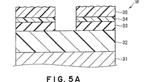
この場合に、エッチング前のウエハWにおいては、図4に示すように、シリコン基板31の上に層間絶縁層としてlow−k膜である有機系材料膜32が形成されている。そして、当該有機系材料膜32の上に、ハードマスクとして所定のパターンの無機系材料膜33が形成されている。さらにその上に、BARC層34が形成され、その上に所定パターンのレジスト膜35が形成されている。
無機系材料膜33は、一般的にハードマスクとして用いられる材料で構成されている。シリコン酸化物、シリコン窒化物、シリコン酸窒化物等が、好適な例として挙げられ得る。
エッチング対象膜である有機系材料膜32は、典型的には上述のように、層間絶縁膜として用いられるlow−k膜である。従って、有機系材料膜42の比誘電率は、従来の層間絶縁層材料であるシリコン酸化物よりも極めて小さい。このような有機系材料のlow−k膜としては、例えば、ポリオルガノシロキサン架橋ビスベンゾシクロブテン樹脂(BCB)やDowChemical社製のSiLK(商品名)やFLARE(商品名)等のポリアリーレンエーテル樹脂(PAE)、メチルシルセスキオキサン(MSQ)等の有機ポリシロキサン樹脂、等がある。ここで、有機ポリシロキサンとは、以下に示すように、シリコン酸化膜の結合構造中にC、Hを含む官能基を含む構造を有するものをいう。以下に示す構造中、Rはメチル基、エチル基、プロピル基等のアルキル基もしくはその誘導体、またはフェニル基等のアリール基もしくはその誘導体を示す。

次に、有機系材料膜32が、レジスト膜35および無機系材料膜33をマスクとしてトレンチエッチングされる。まず、図1の装置のゲートバルブ24が開けられて、搬送アームにて図5Aに示す構造のウエハWがチャンバー1内に搬入され、支持テーブル2上に載置される。その後、搬送アームが退避されてゲートバルブ24が閉じられ、支持テーブル2が図1に示す位置まで上昇される。また、排気系20の真空ポンプにより、排気ポート19を介してチャンバー1内が所定の真空度とされる。
その後、チャンバー1内に処理ガス供給系15から所定の処理ガス、例えばN2ガスおよびO2ガス、が例えば0.1〜1L/min(100〜1000sccm)で導入され、チャンバー1内が例えば133Pa(1000mT0rr)以下の所定の圧力に維持される。この状態で、高周波電源10から支持テーブル2に、周波数が50〜150MHzの高周波電力が供給される。この際の単位面積当たりのパワーは、約0.5〜約10W/cm2の範囲であることが好ましい。このとき、直流電源13から静電チャック6の電極6aに所定の電圧が印加され、ウエハWは例えばクーロン力により静電チャック6に吸着される。
このように下部電極である支持テーブル2に高周波電力が印加されることにより、上部電極であるシャワーヘッド16と下部電極である支持テーブル2との間の処理空間に高周波電界が形成される。これにより、処理空間に供給された処理ガスがプラズマ化され、そのプラズマにより有機系材料膜32がエッチングされる。
このエッチング工程の際に、マルチポール状態のリング磁石21により、処理空間の周囲に図2に示すような磁場が形成され得る。この場合、プラズマ閉じこめ効果が発揮され、本実施形態のようにプラズマの不均一が生じやすい高周波数の場合でも、ウエハWのエッチングレートが均一化され得る。また、膜の種類によっては、このような磁場の効果がない場合もある。その場合には、セグメント磁石22を回転させて、処理空間の周囲に実質的に磁場が形成されない状態にして処理を行ってもよい。
上記磁場が形成された場合には、支持テーブル2上のウエハWの周囲に設けられた導電性または絶縁性のフォーカスリング5により、プラズマ処理の均一化効果を一層高めることができる。すなわち、ウエハ周辺部のプラズマ密度が高く、ウエハ周辺部のエッチングレートがウエハ中心部のエッチングレートに比べて大きい場合は、シリコンやSiC等の導電性材料で形成されたフォーカスリングを用いることによって、フォーカスリング領域までが下部電極として機能するため、プラズマ形成領域がフォーカスリング5上まで広がり、ウエハWの周辺部におけるプラズマ処理が促進されエッチングレートの均一性が向上される。一方、ウエハ周辺部のプラズマ密度が低く、ウエハ周辺部のエッチングレートがウエハ中心部のエッチングレートに比べて小さい場合は、石英等の絶縁性材料で形成されたフォーカスリングを用いることによって、フォーカスリング5とプラズマ中の電子やイオンとの間で電荷が授受され得ないので、プラズマを閉じこめる作用が増大され得てエッチングレートの均一性が向上される。
また、必要に応じて、図3に示すイオン引き込み用の高周波電源26から500KHz〜27MHzの範囲の高周波電力を支持テーブル2に印加して、イオンエネルギーを制御して有機系材料膜32のエッチングレートをより上昇させるようにしてもよい。
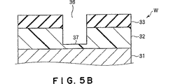
本実施形態においては、図5Bに示すように、トレンチ36を形成する際に、エッチングを有機系材料膜32の途中で停止させて、トレンチ36の底部に平坦部37を形成する。この場合に、イオンの垂直方向のエネルギーが大きいと、平坦部37のエッジ部分に、図6に示すように、さらに下方に伸びる微小な溝であるマイクロトレンチング38が発生することがある。このようなマイクロトレンチングは、埋め込み不良や電荷の集中の原因となるため、極力抑制する必要がある。そこで、本実施形態においては、マイクロトレンチングを生じ難くするため、高周波電源10から支持テーブル2に供給する高周波電力の周波数を50〜150MHzとしている。
以下、その理由について説明する。
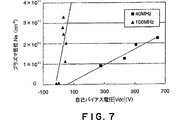
本発明者等の検討結果によると、有機系材料膜のエッチングでは、プラズマ密度が支配的であってイオンエネルギーの寄与が小さいことが判明している。一方、マイクロトレンチングは、イオンの垂直方向のエネルギーが大きいと発生する。したがって、上記有機系材料膜32のトレンチエッチングを行う際に、マイクロトレンチングを抑制して有機系材料膜32を高エッチングレートでエッチングするためには、プラズマ密度が高く、かつ、イオンエネルギーが小さい条件でエッチングを行えばよい。この場合に、プラズマのイオンエネルギーは、エッチングの際における電極の自己バイアス電圧と間接的に対応するから、マイクロトレンチングを抑制しつつ高エッチングレートで有機材料膜32をエッチングするためには、結局、高プラズマ密度かつ低バイアスの条件でエッチングすることが必要である。そして、以下に説明する図7から明らかなように、高周波電力の周波数を従来よりも高くすることにより、高プラズマ密度かつ低バイアスの条件でエッチングすることができる。
図7は、高周波電力の周波数が40MHz、100MHzにおける自己バイアス電圧の絶対値|Vdc|とプラズマ密度Neとの関係を示す図である。横軸が自己バイアス電圧Vdcであり、縦軸がプラズマ密度Neである。ここで、プラズマガスとしては、実際のエッチングガスではなく、評価用にArが用いられた。なお、各周波数において、印加する高周波パワーを変化させることにより、プラズマ密度Neおよび自己バイアス電圧の絶対値|Vdc|が変化された。つまり、各周波数とも、印加する高周波パワーが大きくなるほど、プラズマ密度Neおよび自己バイアス電圧|Vdc|はともに大きくなる。また、プラズマ密度は、マイクロ波干渉計により測定された。
図7に示すように、高周波電力の周波数が従来の40MHzの場合には、有機系材料膜のエッチングレートを高くすべくプラズマ密度を上昇させると、|Vdc|も大きく上昇し、高プラズマ密度かつ低自己バイアス電圧を実現することが困難であった。一方、高周波電力の周波数が従来よりも高い100MHzの場合には、プラズマ密度を上昇させても|Vdc|はあまり上昇せず、ほぼ100V以下に抑えられた。すなわち、高プラズマ密度および低自己バイアス電圧が実現可能であることが見出された。
このような結果に基づいて、高周波電源10から支持テーブル2に供給される高周波電力の周波数を従来よりも高い50MHzとした。ただし、プラズマ形成用の高周波電力の周波数が150MHzを超えると、プラズマの均一性が損なわれ得る。このため、プラズマ形成用の高周波電力の周波数は150MHz以下とすることが好ましい。特に上記効果を有効に発揮させるためには、プラズマ形成用の高周波電力の周波数は70〜100MHzが好ましい。
この場合に、さらなるエッチングレートの上昇を目的として、上述のように、高周波電源26から500kHz〜27MHzの高周波電力が重畳して印加されると、そのイオン引き込み効果によりマイクロトレンチングが発生しやすくなる。
これに対しては、チャンバー1内の圧力を53Pa以上の高い値に設定する。これにより、イオン同士が衝突して散乱するので、マイクロトレンチングが有効に抑制され得る。ただし、チャンバー1内の圧力が133Paを超えると、CDシフトが大きくなる。したがって、高周波電源26からの高周波電力を重畳させて大きなエッチングレートを得つつ、マイクロトレンチングを有効に抑制し、かつ、CDシフトを所望の範囲に維持するためには、チャンバー内の圧力は53〜133Paが好ましい。もちろん、高周波電源26からの高周波電力を重畳させない場合にも、チャンバー1内の圧力を53Pa以上と高い値に設定すれば、より有効にマイクロトレンチングを抑制することができる。
また、エッチングの際の処理ガスのチャンバー内滞在時間いわゆるレジデンスタイムは、70〜180msecであることが好ましい。この時間範囲が、ほぼ上記圧力範囲に対応する。なお、レジデンスタイムとは、処理ガスのチャンバー1内のエッチングに寄与する部分における滞留時間をいう。具体的には、ウエハW面積に電極間距離を掛けて求めた有効チャンバー体積をV(m3)(ウエハ外側のガスはエッチングに寄与しないから、エッチングに寄与するガスが存在する部分の体積を用いる)、排気速度をS(m3/sec)、チャンバー内圧力をp(Pa)、総流量をQ(Pa・m3/sec)とすると、レジデンスタイムτは、以下の式で求めることができる。
τ=V/S=pV/Q(sec)
なお、上記マイクロトレンチングは、トレンチ36の平坦部37の幅が0.5μmのときに発生しやすい。従って、本発明は、平坦部37の幅が0.5μm以上のときに大きな効果を発揮する。
次に、有機系材料膜に実際にトレンチを形成した実験結果について説明する。ここでは、図1の装置が用いられ、ウエハWとして300mmウエハが用いられ、エッチングガスとして、N2ガスおよびH2ガスが用いられ、電極間ギャップが40mmとされ、100MHzおよび3.2MHzの2周波数の高周波電力が重畳されて印加された。ここで、高周波電力のトータルのパワーが2400Wとされ、3.2MHzの高周波電力のパワーが800Wとされて、エッチングレートが高められた。そして、チャンバー内圧力は13.3Pa(100mTorr)、60Pa(450mTorr)、106.5Pa(800mTorr)と変化され、それぞれの圧力条件でトレンチエッチングが行われた。なお、圧力13.3Paの際には、ガス流量がN2ガス:0.5L/min、H2ガス:0.5L/minとされ、圧力60Pa、106.5Paの際には、ガス流量がN2ガス:0.65L/min、H2ガス:0.65L/minとされた。また、圧力が13.3Pa、60Pa、106.5Paの時のレジデンスタイムは、それぞれ、22.3msec、77.3msec、137.5msecであった。用いられたウエハWは、図4に示すものと同様で、シリコン基板上に有機系材料膜32としてSiLK(商品名)が形成され、その上にハードマスクとして機能する無機系材料膜33としてSiO2が形成され、さらにその上にBARC層34及びレジスト膜35が形成された構造であった。
レジスト膜35をマスクとしてBARC層34および無機系材料膜33がエッチングされた後、上記各条件にてトレンチが形成された。その後、各圧力条件毎のSiLK(商品名)のエッチングレート、マイクロトレンチ指数及びCDシフトの値が測定された。
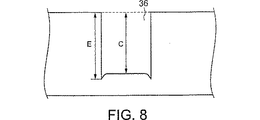
マイクロトレンチ指数は、図8に示すように、0.5μm幅のトレンチのエッジの長さEに対する中央の長さCの比であるC/Eの値に100を掛けて%表示されている。この値が100%に近ければ、マイクロトレンチがなく良好なエッチング状態であり、90%以上あれば良好である。
また、CDシフトは、エッチング後にハードマスク(SiO2膜)の上方から見たときのトップのトレンチ幅(ここでは、0.25μm)からのずれ量を示すものである。CDシフトは、トップより狭くなっている場合にはマイナス、広くなっている場合はプラスの値となる。その絶対値が小さければ、良好なエッチング状態であり、絶対値が10nm以下であれば良好である。
実験結果を図9及び図10に示す。図9に示すように、チャンバー内圧力が上昇するにつれてエッチングレートが低下していることがわかる。
一方、図10に示すように、チャンバー内圧力が上昇するにつれてマイクロトレンチ指数が上昇していることがわかる。そして、13.3Pa(100mTorr)ではマイクロトレンチ指数が好ましい値90%よりも低い88%であったのに対し、60Pa(450mTorr)では91%(>90%)、106.5Pa(800mTorr)では93%(>90%)であった。したがって、チャンバー内圧力が53Pa(400mTorr)以上であれば、マイクロトレンチが極めて発生し難いことが確認された。
また、図10に示すように、チャンバー内圧力が上昇するにしたがってCDシフトの絶対値が小さくなる傾向にある一方、チャンバー内圧力が133Pa(1000mTorr)を超えるとCDシフトがプラス側の大きな値となることが予想される。したがって、エッチングレート上昇を目的として3.2MHzの高周波電力が重畳された場合、チャンバー内圧力は約53〜約133Pa(約400〜約1000mTorr)が好ましいことが確認された。この時、レジデンスタイムは、約70〜約180msecである。なお、詳細については省略するが、100MHzの場合が50MHz未満の場合よりもマイクロトレンチ指数が高いことも確認された。
次に、有機系材料膜に実際にトレンチを形成した他の実験結果について説明する。ここでも、図1の装置が用いられ、ウエハWとして300mmウエハが用いられたが、エッチングガスとして、NH3ガスが用いられ、電極間ギャップが20mmとされ、100MHzおよび3.2MHzの2周波数の高周波電力が重畳されて印加された。
トレンチ形成の実験結果を示す前に、上記条件下で各パラメータを変化させた場合の特性について、図11乃至図14を用いて示す。
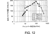
図11は、前記条件下での、チャンバー内圧力とプラズマ密度Neとの関係を示している。図12は、当該条件下での、チャンバー内圧力と自己バイアス電圧の絶対値|Vdc|との関係を示している。図11及び図12に示されたプロットデータは、ガス流量を100sccmとしてチャンバー内圧力を10mTorr(1.33Pa)近傍に調整した圧力条件、ガス流量を200sccmとしてチャンバー内圧力を10(1.33Pa)〜約100mTorr(約13.3Pa)に調整した圧力条件、更に、ガス流量を600sccmとしてチャンバー内圧力を100mTorr(約13.3Pa)以上とした圧力条件、に対応している。
また、図11及び図12のデータについては、3.2MHzの高周波電力は重畳されず、100MHzの高周波電力のパワーは2400Wとされた。
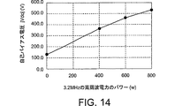
図13は、チャンバー内圧力を30mTorrとして、100MHzの高周波電力のパワーと自己バイアス電圧の絶対値|Vdc|との関係を示している。
図14は、チャンバー内圧力を30mTorrとし、100MHzの高周波電力のパワーを2400Wとして、3.2MHzの高周波電力を重畳した場合の当該高周波電力のパワーと自己バイアス電圧の絶対値|Vdc|との関係を示している。
図11乃至図14の特性から、以下のような知見が得られる。
形状制御性を高めるため等の理由で、10mTorr(1.33Pa)〜100mTorr(13.3Pa)のような低圧範囲を使用する場合、イオン同士の衝突・散乱の程度が小さい。このため、3.2MHzの高周波電力は重畳されるべきでなく、また、マイクロトレンチング抑制のためにプラズマのイオンエネルギーを抑制すべく自己バイアス電圧を比較的低くしておくべきである。また、ハードマスクとなるシリコン酸化膜などのスパッタレートを許容範囲に抑えるためには、自己バイアス電圧の上限値は300V程度とすることが好ましい。このような条件において好適な100MHzの高周波電力のパワーは、1000W(1.42W/cm2)〜5000(7.08W/cm2)Wであり、対応するチャンバー内のプラズマ密度は、5×1010〜1×1011cm−3である。
一方、エッチングレートを高めるため等の理由で、400mTorr(53Pa)〜1000mTorr(133Pa)のような高圧範囲を使用する場合、イオン同士の衝突・散乱の程度が大さい。このため、エッチングレートの更なる上昇を目的として3.2MHzの高周波電力が重畳されることが、許容される。また、自己バイアス電圧の上限値についても、低圧の場合よりも高く、ハードマスクとなるシリコン酸化膜などのスパッタレートを許容範囲に抑えるためには、600V程度とすることが好ましい。このような条件において好適な100MHzの高周波電力のパワーは、1000W(1.42W/cm2)〜5000(7.08W/cm2)Wであり、好適な3.2MHzの高周波電力のパワーは、800W(1.13W/cm2)以下であり、対応するチャンバー内のプラズマ密度は、1×1011〜2×1011cm−3である。
さて、前記条件下でのトレンチ形成の実験に用いられたウエハWは、図4に示すものと同様で、シリコン基板上に有機系材料膜32としてSiLK(商品名)が形成され、その上にハードマスクとして機能する無機系材料膜33としてSiO2が形成され、さらにその上にBARC層34及びレジスト膜35が形成された構造であった。
レジスト膜35をマスクとしてBARC層34および無機系材料膜33がエッチングされた後、トレンチが形成された。この時、チャンバー内圧力は30mTorrであり、3.2MHzの高周波電力のパワーは重畳されず、100MHzの高周波電力のパワーは、2400Wであった。トレンチは、ウエハ中央部で209nm/minのエッチングレートで、0.12μmの幅に形成され、マイクロトレンチ指数は極めて良好であった。
なお、本発明は上記実施の形態に限定されることなく、種々変更可能である。例えば、上記実施形態では、何も形成されていない有機系材料膜にトレンチエッチングにより平坦な溝を形成する場合が示されているが、図15Aに示すような下層43に繁がる層間配線のためのホール41を予め有する有機系材料膜42に対し図15Bに示すような平坦部47を有するトレンチ46を形成する場合にも本発明は適用することができる。
また、上記実施形態では、磁場形成手段として永久磁石からなる複数のセグメント磁石がチャンバーの周囲にリング状に配置されてなるマルチポール状態のリング磁石が用いられたが、処理空間の周囲に磁場を形成してプラズマを閉じこめることができれば、この態様に限定されるものではない。また、このようなプラズマ閉じこめ用の周辺磁場は、必ずしも必要ではない。つまり、磁場が存在しない状態でエッチングを行ってもよい。また、処理空間に水平磁場を印加して直交電磁界中でプラズマエッチングを行うプラズマエッチング処理にも本発明は適用可能である。
さらに、上記実施形態では下部電極にプラズマ形成用の高周波電力が印加されているが、これに限らず、上部電極に印加されてもよい。さらにまた、上記実施形態では有機系材料膜としてlow−k膜を用いたが、これに限定されることなく、O、C、Hを含む他の膜やSi、O、C、Hを含む他の膜であってもよい。また、層構造も、図4に示すものに限定されない。更には、被処理基板として半導体ウエハを用いた場合について示したが、これに限らず、LCD基板等の他の被処理基板の有機系材料膜のプラズマ処理にも適用することができる。
【図面の簡単な説明】
図1は、本発明の一実施の形態のプラズマエッチング装置を示す概略断面図である。
図2は、図1のプラズマエッチング装置のチャンバーの周囲に配置されたリング磁石を模式的に示す水平断面図である。
図3は、プラズマ生成用の高周波電源とイオン引き込み用の高周波電源とを備えたプラズマ処理装置を部分的に示す概略断面図である。
図4は、本発明のプラズマエッチングが適用されるウエハの構造例を示す断面図である。
図5A及び図5Bは、本発明のプラズマエッチングのエッチング状態を説明するための図である。
図6は、マイクロトレンチングを説明するための模式図である。
図7は、アルゴンガスのプラズマにおいて、高周波電力の周波数が40MHzと100MHzとの場合の、自己バイアス電圧の絶対値|Vdc|とプラズマ密度Neとの関係を示す図である。
図8は、マイクロトレンチ指数を説明するための模式図である。
図9は、チャンバー内圧力とエッチングレートとの関係を説明するための図である。
図10は、チャンバー内圧力とマイクロトレンチ指数との関係、及び、チャンバー内圧力とCDシフトとの関係を説明するための図である。
図11は、NH3ガスのプラズマにおいて、チャンバー内圧力とプラズマ密度Neとの関係を示す図である。
図12は、NH3ガスのプラズマにおいて、チャンバー内圧力と自己バイアス電圧の絶対値|Vdc|との関係を示す図である。
図13は、NH3ガスのプラズマにおいて、チャンバー内圧力を30mTorrとした場合の、100MHzの高周波電力のパワーと自己バイアス電圧の絶対値|Vdc|との関係を示す図である。
図14は、NH3ガスのプラズマにおいて、チャンバー内圧力を30mTorrとし、100MHzの高周波電力のパワーを2400Wとして、3.2MHzの高周波電力を重畳した場合において、3.2MHzの高周波電力のパワーと自己バイアス電圧の絶対値|Vdc|との関係を示す図である。
図15Aは、本発明のプラズマエッチングが適用されるウエハの他の構造例を示す断面図である。
図15Bは、図15Aのウエハに対するエッチング状態を説明するための図である。Technical field
The present invention relates to a plasma etching method for plasma-etching an organic material film such as a low dielectric constant film (low-k film) formed on a substrate to be processed such as a semiconductor wafer to the middle of the film.
Background technology
In the wiring formation process of the semiconductor device, the interlayer insulating film formed between the wiring layers is etched to make the wiring layer conductive. As an interlayer insulating film, a film having a lower dielectric constant has recently been demanded in order to further increase the speed of semiconductor devices. An organic material film is being used as such a low dielectric constant film.
Etching of the organic material film is performed by plasma etching. Specifically, a pair of opposing electrodes that are vertically opposed to each other are provided in the chamber, a semiconductor wafer (hereinafter simply referred to as a wafer) is placed on the lower electrode, and the lower electrode has a frequency of about 13.56 to 40 MHz. Etching is performed by supplying high-frequency power.
However, in trench etching of organic material films, for example, when the bottom of a groove formed by etching is stopped in the middle of the film, such as a single damascene structure or a dual damascene structure without a stop layer, is made flat. However, there is a problem that micro-trenching occurs at the edge portion of the bottom of the groove. When micro-trenching occurs, there is a disadvantage in that, during the subsequent formation of the buried layer, a defective filling or concentration of charges occurs.
Summary of the Invention
The present invention has been made in view of such circumstances, and suppresses the occurrence of micro-trenching when plasma etching an organic material film so that a groove having a flat bottom is formed in the middle of the film. It is an object of the present invention to provide a plasma etching method that can be used.
According to the examination results of the present inventors, it has been found that, in the etching of the organic material film, the plasma density is dominant and the contribution of ion energy is small. On the other hand, microtrenching occurs when the energy of ions in the vertical direction is large. Therefore, in order to suppress microtrenching and etch the organic material film at a high etching rate, it is necessary that the plasma density is high and the ion energy is low to some extent. In this case, the ion energy of the plasma indirectly corresponds to the self-bias voltage of the electrode during etching. Therefore, in order to etch the organic material film at a high etching rate while suppressing microtrenching, it is eventually necessary to perform etching under conditions of high plasma density and low bias. According to further examination results by the present inventors, it has been found that if the frequency of the high frequency power applied to the electrode is high, a state in which the plasma density is high and the self-bias voltage is small can be realized.
The present invention is an arrangement in which a pair of electrodes are arranged opposite to each other in a chamber, and the substrate to be processed is supported by one electrode so that the substrate to be processed having an organic material film is disposed between both electrodes. A high-frequency electric field is applied to at least one electrode to form a high-frequency electric field between the pair of electrodes, a processing gas is supplied into the chamber, and a plasma of the processing gas is formed by the electric field. An etching step of plasma-etching the organic material film of the substrate to be processed so as to form a groove having a flat bottom partway through the film, and applying to the at least one electrode in the etching step The plasma etching method is characterized in that the frequency of the high-frequency power is 50 to 150 MHz.
According to the present invention, since the frequency of the high-frequency power applied to the electrode is 50 to 150 MHz, which is higher than the conventional one, a low self-bias voltage can be realized while being a high-density plasma. Thereby, the organic material film can be etched at a high etching rate while suppressing microtrenching.
Preferably, in the etching step, the pressure in the chamber is 1.33-13.3 Pa.
Preferably, in the etching step, the plasma density in the chamber is 5 × 10 5. 10 ~ 1x10 11 cm -3 It is.
The high frequency power is preferably applied to an electrode that supports the substrate to be processed. In this case, a second high frequency power of 500 kHz to 27 MHz may be applied to the electrode supporting the substrate to be processed so as to be superimposed on the high frequency power. Thus, the etching rate can be further increased by superimposing the second high-frequency power having a lower frequency.
On the other hand, when the second high-frequency power is superimposed, microtrenching is more likely to occur due to the ion drawing effect. This can be dealt with by setting the pressure in the chamber to a high value of 53 Pa or more. By increasing the pressure in the chamber in this way, ions collide and scatter, so that microtrenching can be effectively suppressed.
Of course, even when the second high-frequency power is not superimposed, microtrenching can be more effectively suppressed by setting the chamber internal pressure to a high value of 53 Pa or higher. However, the CD shift increases when the pressure in the chamber exceeds 133 Pa. Therefore, the pressure in the chamber is preferably 53 to 133 Pa.
In order to superimpose the second high frequency power, the self-bias voltage of the electrode is preferably 600 V or less.
Moreover, in the said etching process, it is preferable that the residence time of the process gas in the said chamber is 70-180 msec.
Alternatively, the effective chamber volume obtained by multiplying the area of the substrate to be processed by the distance between the electrodes is V (m 3 ) And the exhaust speed is S (m 3 / Sec), the value of V / S is preferably 70 to 180 msec.
In addition, the present invention supports a substrate to be processed by one electrode so that a substrate to be processed having an organic material film is disposed between both electrodes in a chamber. A high-frequency electric field is applied to at least one electrode to form a high-frequency electric field between the pair of electrodes, a processing gas is supplied into the chamber, and plasma of the processing gas is formed by the electric field, An etching step of plasma-etching the organic material film of the substrate to be processed by plasma so that a groove having a flat bottom is formed partway through the film, and in the etching step, the pressure in the chamber Is 1.33-13.3 Pa, and the plasma density in the chamber is 5 × 10 5. 10 ~ 1x10 11 cm -3 The plasma etching method is characterized in that the self-bias voltage of the electrode is 300 V or less.
According to the present invention, the pressure in the chamber is 1.33-13.3 Pa, and the plasma density in the chamber is 5 × 10 5. 10 ~ 1x10 11 cm -3 In addition, since plasma is formed under the condition that the electrode self-bias voltage is 300 V or less, the organic material film can be etched at a high etching rate while suppressing microtrenching.
In addition, the present invention supports a substrate to be processed by one electrode so that a substrate to be processed having an organic material film is disposed between both electrodes in a chamber. A high-frequency electric field is applied to at least one electrode to form a high-frequency electric field between the pair of electrodes, a processing gas is supplied into the chamber, and plasma of the processing gas is formed by the electric field, An etching step of plasma-etching the organic material film of the substrate to be processed by plasma so that a groove having a flat bottom is formed partway through the film, and in the etching step, the pressure in the chamber Is 53 to 133 Pa, and the plasma density in the chamber is 1 × 10 11 ~ 2x10 11 cm -3 The plasma etching method is characterized in that the self-bias voltage of the electrode is 600 V or less.
According to the present invention, the pressure in the chamber is 53 to 133 Pa, and the plasma density in the chamber is 1 × 10. 11 ~ 2x10 11 cm -3 In addition, since plasma is formed under the condition that the self-bias voltage of the electrode is 600 V or less, the organic material film can be etched at a high etching rate while suppressing microtrenching.
In the above, the processing gas is, for example, N 2 Gas, H 2 Gas, O 2 Gas, CO gas, NH 3 Gas, C x H y (X and y are natural numbers) and at least one selected from rare gases.
The organic material film may include O, C, and H. Alternatively, the organic material film may include Si, O, C, and H. Typically, the organic material film is a low dielectric constant film (low-k film).
Micro-trenching tends to occur as the groove width increases. Therefore, the present invention is particularly effective when the flat portion has a width of 0.5 μm or more.
By the way, according to Paschen's law, the discharge start voltage Vs takes a minimum value (Paschen minimum value) and takes a Paschen minimum value when the product pd of the gas pressure p and the inter-electrode distance d is a certain value. The value of the product pd decreases as the frequency of the high frequency power increases. Therefore, when the frequency of the high frequency power is large, in order to reduce the discharge start voltage Vs to facilitate and stabilize the discharge, it is necessary to reduce the inter-electrode distance d if the gas pressure p is constant. Therefore, in the present invention, the distance between the electrodes is preferably less than 50 mm. Moreover, the residence time of the gas in a chamber can be shortened because the distance between electrodes is less than 50 mm. Thereby, the reaction product can be efficiently discharged, and the effect that the etching stop can be reduced is also obtained.
BEST MODE FOR CARRYING OUT THE INVENTION
Hereinafter, embodiments of the present invention will be described with reference to the accompanying drawings.
FIG. 1 is a cross-sectional view showing a plasma etching apparatus used for carrying out the present invention. This etching apparatus is airtightly configured and includes a stepped
In the
A
In addition, it is preferable that the distance between these electrodes is set to less than 50 mm. The reason is as follows.
According to Paschen's law, the discharge start voltage Vs takes a minimum value (Paschen minimum value) and a Paschen minimum value pd when the product pd of the gas pressure p and the interelectrode distance d is a certain value. The value of becomes smaller as the frequency of the high-frequency power increases. Accordingly, when the frequency of the high frequency power is large as in the present embodiment, in order to make the discharge start voltage Vs small and facilitate discharge and stabilize, the inter-electrode distance d is made small if the gas pressure p is constant. There is a need to. For this reason, the distance between the electrodes is preferably less than 50 mm. Moreover, the residence time of the gas in a chamber can be shortened because the distance between electrodes is less than 50 mm. Thereby, the reaction product can be efficiently discharged, and the effect that the etching stop can be reduced is also obtained.
However, if the distance between the electrodes is too small, the pressure distribution (pressure difference between the central portion and the peripheral portion) on the surface of the wafer W that is the substrate to be processed increases. In this case, problems such as a decrease in etching uniformity may occur. Regardless of the gas flow rate, in order to make the pressure difference smaller than 0.27 Pa (2 mTorr), the distance between the electrodes is preferably 35 mm or more.
An
A coolant channel (not shown) is formed inside the support table 2. The wafer W can be controlled to a predetermined temperature by circulating an appropriate refrigerant therein. In addition, in order to efficiently transmit the cold heat from the refrigerant to the wafer W, a gas introduction mechanism (not shown) for supplying He gas to the back surface of the wafer W is provided. Further, a
A
Such a processing gas reaches the
An
On the other hand, a
As shown in the horizontal sectional view of FIG. 2, the
Further, when the magnetic field as described above is formed in the periphery of the processing space, it is desirable that the magnetic field intensity on the
Here, “substantially no magnetic field in the wafer arrangement region” means that a magnetic field that affects the etching process in the wafer arrangement region is not formed. That is, the case where there is a magnetic field that does not substantially affect the wafer processing is included.
In the state shown in FIG. 2, a magnetic field having a magnetic field strength of 0.42 mT (4.2 Gauss) or less is applied to the periphery of the wafer, for example. Thereby, the function of confining plasma is exhibited.
When a magnetic field is formed by such a multi-pole ring magnet, a portion corresponding to the magnetic pole of the wall portion of the chamber 1 (for example, a portion indicated by P in FIG. 2) may be locally scraped. . Therefore, the
Each of the
Since the state of the magnetic field changes according to the arrangement of the segment magnets, various magnetic field strength profiles can be formed by changing the arrangement of the segment magnets in various ways. Therefore, it is preferable to arrange the segment magnets so that the required magnetic field strength profile can be obtained.
The number of segment magnets is not limited to this example. Further, the cross-sectional shape is not limited to a rectangle as in this example, and an arbitrary shape such as a circle, a square, or a trapezoid can be adopted. The magnet material constituting the
In order to adjust the plasma density and the ion drawing action, the high frequency for plasma generation and the second high frequency for drawing ions in the plasma may be superimposed. Specifically, as shown in FIG. 3, in addition to the high-
Next, a processing operation when a low dielectric constant film (low-k film) that is an organic material film is etched by the plasma etching apparatus configured as described above will be described.
In this case, in the wafer W before etching, as shown in FIG. 4, an
The
The
Next, the
Thereafter, a predetermined processing gas such as N 2 Gas and O 2 Gas is introduced at, for example, 0.1 to 1 L / min (100 to 1000 sccm), and the inside of the
Thus, by applying the high frequency power to the support table 2 that is the lower electrode, a high frequency electric field is formed in the processing space between the
During this etching step, a magnetic field as shown in FIG. 2 can be formed around the processing space by the
When the magnetic field is formed, the effect of uniformizing plasma processing can be further enhanced by the conductive or insulating
Further, if necessary, a high frequency power in the range of 500 KHz to 27 MHz is applied to the support table 2 from the high
In the present embodiment, as shown in FIG. 5B, when forming the
The reason will be described below.
According to the examination results of the present inventors, it has been found that in the etching of the organic material film, the plasma density is dominant and the contribution of ion energy is small. On the other hand, microtrenching occurs when the energy of ions in the vertical direction is large. Therefore, when performing trench etching of the
FIG. 7 is a diagram showing the relationship between the absolute value | Vdc | of the self-bias voltage and the plasma density Ne when the frequency of the high-frequency power is 40 MHz and 100 MHz. The horizontal axis is the self-bias voltage Vdc, and the vertical axis is the plasma density Ne. Here, as the plasma gas, Ar was used for evaluation, not an actual etching gas. At each frequency, the plasma density Ne and the absolute value | Vdc | of the self-bias voltage were changed by changing the applied high frequency power. That is, for each frequency, as the applied high frequency power increases, both the plasma density Ne and the self-bias voltage | Vdc | increase. The plasma density was measured with a microwave interferometer.
As shown in FIG. 7, when the frequency of the high frequency power is 40 MHz in the past, if the plasma density is increased to increase the etching rate of the organic material film, | Vdc | It was difficult to realize a low self-bias voltage. On the other hand, when the frequency of the high frequency power is 100 MHz, which is higher than the conventional frequency, | Vdc | does not increase so much even if the plasma density is increased, and is suppressed to about 100 V or less. That is, it has been found that high plasma density and low self-bias voltage are feasible.
Based on such results, the frequency of the high-frequency power supplied from the high-
In this case, for the purpose of further increasing the etching rate, when high frequency power of 500 kHz to 27 MHz is superimposed and applied from the high
For this, the pressure in the
Further, the residence time of the processing gas in the chamber during etching, so-called residence time, is preferably 70 to 180 msec. This time range substantially corresponds to the pressure range. The residence time refers to a residence time in a portion that contributes to etching of the processing gas in the
τ = V / S = pV / Q (sec)
The micro-trenching is likely to occur when the width of the
Next, an experimental result in which a trench is actually formed in an organic material film will be described. Here, the apparatus of FIG. 1 is used, a 300 mm wafer is used as the wafer W, and N is used as the etching gas. 2 Gas and H 2 Gas was used, the gap between the electrodes was 40 mm, and high frequency power of two frequencies of 100 MHz and 3.2 MHz was superimposed and applied. Here, the total power of the high frequency power is 2400 W, the power of the high frequency power of 3.2 MHz is 800 W, and the etching rate is increased. The pressure in the chamber was changed to 13.3 Pa (100 mTorr), 60 Pa (450 mTorr), and 106.5 Pa (800 mTorr), and trench etching was performed under each pressure condition. When the pressure is 13.3 Pa, the gas flow rate is N. 2 Gas: 0.5 L / min, H 2 Gas: 0.5 L / min. When the pressure is 60 Pa and 106.5 Pa, the gas flow rate is N. 2 Gas: 0.65 L / min, H 2 Gas: 0.65 L / min. The residence times when the pressure was 13.3 Pa, 60 Pa, and 106.5 Pa were 22.3 msec, 77.3 msec, and 137.5 msec, respectively. The used wafer W is the same as that shown in FIG. 4, SiLK (trade name) is formed on the silicon substrate as the
After the
As shown in FIG. 8, the micro-trench index is expressed in% by multiplying the value of C / E, which is the ratio of the center length C to the edge length E of the 0.5 μm wide trench, by 100. If this value is close to 100%, there is no microtrench and the etching state is good, and if it is 90% or more, it is good.
Also, CD shift is caused by a hard mask (
The experimental results are shown in FIGS. As shown in FIG. 9, it can be seen that the etching rate decreases as the pressure in the chamber increases.
On the other hand, as shown in FIG. 10, it can be seen that the micro-trench index increases as the pressure in the chamber increases. At 13.3 Pa (100 mTorr), the micro-trench index was 88%, which is lower than the preferred value of 90%, whereas at 60 Pa (450 mTorr), 91% (> 90%), and at 106.5 Pa (800 mTorr), 93 % (> 90%). Therefore, it was confirmed that when the pressure in the chamber was 53 Pa (400 mTorr) or more, micro-trench was hardly generated.
Also, as shown in FIG. 10, the absolute value of the CD shift tends to decrease as the chamber pressure increases. On the other hand, when the chamber pressure exceeds 133 Pa (1000 mTorr), the CD shift increases to a large value on the plus side. It is expected to be. Therefore, it was confirmed that the chamber pressure is preferably about 53 to about 133 Pa (about 400 to about 1000 mTorr) when high frequency power of 3.2 MHz is superimposed for the purpose of increasing the etching rate. At this time, the residence time is about 70 to about 180 msec. Although details are omitted, it was also confirmed that the micro-trench index was higher in the case of 100 MHz than in the case of less than 50 MHz.
Next, another experimental result in which a trench is actually formed in an organic material film will be described. Here again, the apparatus of FIG. 1 was used, and a 300 mm wafer was used as the wafer W, but
Before showing the experimental results of trench formation, the characteristics when each parameter is changed under the above conditions will be described with reference to FIGS.
FIG. 11 shows the relationship between the pressure in the chamber and the plasma density Ne under the above conditions. FIG. 12 shows the relationship between the pressure in the chamber and the absolute value | Vdc | of the self-bias voltage under the above conditions. The plot data shown in FIG. 11 and FIG. 12 are the pressure conditions in which the gas flow rate is 100 sccm and the pressure in the chamber is adjusted to around 10 mTorr (1.33 Pa), the gas flow rate is 200 sccm, and the chamber pressure is 10 (1.33 Pa). To a pressure condition adjusted to about 100 mTorr (about 13.3 Pa), and a pressure condition where the gas flow rate is 600 sccm and the pressure in the chamber is 100 mTorr (about 13.3 Pa) or more.
11 and 12, the high frequency power of 3.2 MHz is not superimposed, and the power of the high frequency power of 100 MHz is 2400 W.
FIG. 13 shows the relationship between the power of high-frequency power of 100 MHz and the absolute value | Vdc | of the self-bias voltage when the pressure in the chamber is 30 mTorr.
FIG. 14 shows the relationship between the power of the high-frequency power and the absolute value | Vdc | of the self-bias voltage when the pressure in the chamber is 30 mTorr, the power of the high-frequency power of 100 MHz is 2400 W, and the high-frequency power of 3.2 MHz is superimposed. Is shown.
The following knowledge is obtained from the characteristics shown in FIGS.
When a low pressure range such as 10 mTorr (1.33 Pa) to 100 mTorr (13.3 Pa) is used for reasons such as improving shape controllability, the degree of collision and scattering between ions is small. For this reason, the high frequency power of 3.2 MHz should not be superimposed, and the self-bias voltage should be relatively low in order to suppress the ion energy of the plasma in order to suppress microtrenching. Further, in order to keep the sputtering rate of a silicon oxide film or the like serving as a hard mask within an allowable range, the upper limit value of the self-bias voltage is preferably about 300V. The power of 100 MHz high frequency power suitable under such conditions is 1000 W (1.42 W / cm 2 ) To 5000 (7.08 W / cm) 2 ) W and the plasma density in the corresponding chamber is 5 × 10 10 ~ 1x10 11 cm -3 It is.
On the other hand, when a high pressure range such as 400 mTorr (53 Pa) to 1000 mTorr (133 Pa) is used for reasons such as increasing the etching rate, the degree of collision / scattering between ions is large. For this reason, it is allowed that high frequency power of 3.2 MHz is superimposed for the purpose of further increasing the etching rate. The upper limit value of the self-bias voltage is also higher than in the case of a low pressure, and is preferably about 600 V in order to keep the sputtering rate of a silicon oxide film or the like serving as a hard mask within an allowable range. The power of 100 MHz high frequency power suitable under such conditions is 1000 W (1.42 W / cm 2 ) To 5000 (7.08 W / cm) 2 ) W, and the preferred 3.2 MHz high frequency power is 800 W (1.13 W / cm). 2 ) And the plasma density in the corresponding chamber is 1 × 10 11 ~ 2x10 11 cm -3 It is.
Now, the wafer W used in the trench formation experiment under the above-described conditions is the same as that shown in FIG. 4, and SiLK (trade name) is formed as an
After the
The present invention is not limited to the above-described embodiment, and various modifications can be made. For example, in the above-described embodiment, a case where a flat groove is formed by trench etching in an organic material film on which nothing is formed is shown, but the interlayer wiring that hangs in the
In the above embodiment, a multi-pole ring magnet in which a plurality of segment magnets made of permanent magnets are arranged in a ring shape around the chamber is used as the magnetic field forming means. The present invention is not limited to this mode as long as the plasma can be formed and confined. Further, such a peripheral magnetic field for confining plasma is not always necessary. That is, etching may be performed in the absence of a magnetic field. The present invention is also applicable to a plasma etching process in which a horizontal magnetic field is applied to a processing space and plasma etching is performed in an orthogonal electromagnetic field.
Furthermore, in the above-described embodiment, high-frequency power for plasma formation is applied to the lower electrode, but the present invention is not limited to this, and may be applied to the upper electrode. Furthermore, in the above embodiment, the low-k film is used as the organic material film. However, the present invention is not limited to this, and other films including O, C, and H and other films including Si, O, C, and H are used. This film may be used. Further, the layer structure is not limited to that shown in FIG. Furthermore, although the case where a semiconductor wafer is used as the substrate to be processed has been described, the present invention is not limited to this, and the present invention can also be applied to plasma processing of organic material films on other substrates to be processed such as LCD substrates.
[Brief description of the drawings]
FIG. 1 is a schematic sectional view showing a plasma etching apparatus according to an embodiment of the present invention.
FIG. 2 is a horizontal sectional view schematically showing a ring magnet disposed around the chamber of the plasma etching apparatus of FIG.
FIG. 3 is a schematic cross-sectional view partially showing a plasma processing apparatus provided with a high-frequency power source for plasma generation and a high-frequency power source for ion attraction.
FIG. 4 is a sectional view showing an example of the structure of a wafer to which the plasma etching of the present invention is applied.
5A and 5B are diagrams for explaining the etching state of the plasma etching according to the present invention.
FIG. 6 is a schematic diagram for explaining microtrenching.
FIG. 7 is a diagram showing the relationship between the absolute value | Vdc | of the self-bias voltage and the plasma density Ne when the frequency of the high-frequency power is 40 MHz and 100 MHz in the argon gas plasma.
FIG. 8 is a schematic diagram for explaining the micro-trench index.
FIG. 9 is a diagram for explaining the relationship between the pressure in the chamber and the etching rate.
FIG. 10 is a diagram for explaining the relationship between the pressure in the chamber and the micro-trench index, and the relationship between the pressure in the chamber and the CD shift.
FIG. 11 shows NH 3 It is a figure which shows the relationship between the chamber internal pressure and plasma density Ne in the plasma of gas.
FIG. 12 shows NH 3 FIG. 6 is a diagram showing the relationship between the pressure in the chamber and the absolute value | Vdc | of the self-bias voltage in gas plasma.
FIG. 13 shows NH 3 FIG. 6 is a diagram showing the relationship between the power of high-frequency power of 100 MHz and the absolute value | Vdc | of the self-bias voltage when the pressure in the chamber is 30 mTorr in the gas plasma.
FIG. 14 shows NH 3 In gas plasma, when the pressure in the chamber is 30 mTorr, the power of the high frequency power of 100 MHz is 2400 W, and the high frequency power of 3.2 MHz is superimposed, the absolute value of the power of the 3.2 MHz high frequency power and the self-bias voltage | It is a figure which shows the relationship with Vdc |.
FIG. 15A is a cross-sectional view showing another structural example of a wafer to which the plasma etching of the present invention is applied.
FIG. 15B is a diagram for explaining an etching state on the wafer of FIG. 15A.
Claims (13)
少なくとも一方の電極に高周波電力を印加して前記一対の電極間に高周波電界を形成するとともに、チャンバー内に処理ガスを供給し、前記電界により処理ガスのプラズマを形成し、該プラズマにより前記被処理基板の前記有機系材料膜を当該膜の途中まで平坦な底部を有する溝が形成されるように前記一枚の被処理基板をプラズマエッチングするエッチング工程と、
を備え、
前記エッチング工程において、前記少なくとも一方の電極に印加する高周波電力の周波数が、50〜150MHzであり、
前記エッチング工程において、前記チャンバー内の圧力が、1.33〜13.3Paであり、
前記エッチング工程において、前記チャンバー内の処理ガスの滞在時間は、70〜180msecである
ことを特徴とするプラズマエッチング方法。Arrangement step of supporting a substrate to be processed by one electrode so that a pair of electrodes are arranged opposite to each other in the chamber, and one substrate to be processed having an organic material film is arranged between both electrodes. When,
A high frequency electric field is applied to at least one of the electrodes to form a high frequency electric field between the pair of electrodes, a processing gas is supplied into the chamber, a plasma of the processing gas is formed by the electric field, and the processing target is formed by the plasma. An etching step of plasma-etching the one substrate to be processed so that a groove having a flat bottom is formed in the middle of the organic material film of the substrate ;
With
In the etching process, the high-frequency power of a frequency to be applied to at least one electrode, Ri 50~150MHz der,
In the etching step, the pressure in the chamber is 1.33-13.3 Pa,
The plasma etching method , wherein, in the etching step, a residence time of the processing gas in the chamber is 70 to 180 msec .
ことを特徴とする請求項1に記載のプラズマエッチング方法。2. The plasma etching method according to claim 1, wherein in the etching step, a plasma density in the chamber is 5 × 10 10 to 1 × 10 11 cm −3 .
少なくとも一方の電極に高周波電力を印加して前記一対の電極間に高周波電界を形成するとともに、チャンバー内に処理ガスを供給し、前記電界により処理ガスのプラズマを形成し、該プラズマにより前記被処理基板の前記有機系材料膜を当該膜の途中まで平坦な底部を有する溝が形成されるように前記一枚の被処理基板をプラズマエッチングするエッチング工程と、
を備え、
前記エッチング工程において、前記少なくとも一方の電極に印加する高周波電力の周波数が、50〜150MHzであり、
前記エッチング工程において、前記チャンバー内の圧力が、53〜133Paであり、
前記エッチング工程において、前記チャンバー内の処理ガスの滞在時間は、70〜180msecである
ことを特徴とするプラズマエッチング方法。Arrangement step of supporting a substrate to be processed by one electrode so that a pair of electrodes are arranged opposite to each other in the chamber, and one substrate to be processed having an organic material film is arranged between both electrodes. When,
A high frequency electric field is applied to at least one of the electrodes to form a high frequency electric field between the pair of electrodes, a processing gas is supplied into the chamber, a plasma of the processing gas is formed by the electric field, and the processing target is formed by the plasma. An etching step of plasma-etching the one substrate to be processed so that a groove having a flat bottom is formed in the middle of the organic material film of the substrate ;
With
In the etching process, the high-frequency power of a frequency to be applied to at least one electrode, Ri 50~150MHz der,
In the etching step, the pressure in the chamber is 53 to 133 Pa,
The plasma etching method , wherein, in the etching step, a residence time of the processing gas in the chamber is 70 to 180 msec .
ことを特徴とする請求項3に記載のプラズマエッチング方法。In the etching step, the high-frequency power is applied to an electrode that supports the substrate to be processed, and a second high-frequency power of 500 kHz to 27 MHz is applied to the electrode that supports the substrate to be processed so as to be superimposed on the high-frequency power. The plasma etching method according to claim 3 .
ことを特徴とする請求項3または4に記載のプラズマエッチング方法。5. The plasma etching method according to claim 3 , wherein in the etching step, a self-bias voltage of the electrode is 600 V or less.
ことを特徴とする請求項1乃至5のいずれかに記載のプラズマエッチング方法。The processing gas is selected from N 2 gas, H 2 gas, O 2 gas, CO gas, NH 3 gas, gas represented by C x H y (x and y are natural numbers), and a rare gas. 6. The plasma etching method according to claim 1, wherein the plasma etching method is at least one kind.
ことを特徴とする請求項1乃至6のいずれかに記載のプラズマエッチング方法。The organic material film, O, C, and plasma etching method according to any one of claims 1 to 6, characterized in that it comprises an H.
ことを特徴とする請求項1乃至7のいずれかに記載のプラズマエッチング方法。The organic material film, Si, O, C, and plasma etching method according to any one of claims 1 to 7, characterized in that it comprises an H.
ことを特徴とする請求項1乃至8のいずれかに記載のプラズマエッチング方法。The organic material film, a plasma etching method according to any one of claims 1 to 8, characterized in that a low dielectric constant film.
ことを特徴とする請求項1乃至9のいずれかに記載のプラズマエッチング方法。Width of the flat portion, a plasma etching method according to any one of claims 1 to 9, wherein the at 0.5μm or more.
ことを特徴とする請求項1乃至10のいずれかに記載のプラズマエッチング方法。The distance between the electrodes of the pair of electrodes, a plasma etching method according to any one of claims 1 to 10 and less than 50 mm.
少なくとも一方の電極に高周波電力を印加して前記一対の電極間に高周波電界を形成するとともに、チャンバー内に処理ガスを供給し、前記電界により処理ガスのプラズマを形成し、該プラズマにより前記被処理基板の前記有機系材料膜を当該膜の途中まで平坦な底部を有する溝が形成されるように前記一枚の被処理基板をプラズマエッチングするエッチング工程と、
を備え、
前記エッチング工程において、前記チャンバー内の圧力が1.33〜13.3Paであり、前記チャンバー内のプラズマ密度が5×10¹⁰ 〜1×1011cm−3であって、かつ、電極の自己バイアス電圧が300V以下であり、
前記エッチング工程において、前記チャンバー内の処理ガスの滞在時間は、70〜180msecである
ことを特徴とするプラズマエッチング方法。Arrangement step of supporting a substrate to be processed by one electrode so that a pair of electrodes are arranged opposite to each other in the chamber, and one substrate to be processed having an organic material film is arranged between both electrodes. When,
A high frequency electric field is applied to at least one of the electrodes to form a high frequency electric field between the pair of electrodes, a processing gas is supplied into the chamber, a plasma of the processing gas is formed by the electric field, and the processing target is formed by the plasma. An etching step of plasma-etching the one substrate to be processed so that a groove having a flat bottom is formed in the middle of the organic material film of the substrate ;
With
In the etching step, the pressure in the chamber is 1.33 to 13.3 Pa, the plasma density in the chamber is 5 × 10 10 to 1 × 10 11 cm −3 , and the self-bias of the electrode voltage Ri der less than 300V,
The plasma etching method , wherein, in the etching step, a residence time of the processing gas in the chamber is 70 to 180 msec .
少なくとも一方の電極に高周波電力を印加して前記一対の電極間に高周波電界を形成するとともに、チャンバー内に処理ガスを供給し、前記電界により処理ガスのプラズマを形成し、該プラズマにより前記被処理基板の前記有機系材料膜を当該膜の途中まで平坦な底部を有する溝が形成されるように前記一枚の被処理基板をプラズマエッチングするエッチング工程と、
を備え、
前記エッチング工程において、前記チャンバー内の圧力が53〜133Paであり、前記チャンバー内のプラズマ密度が1×10¹¹ 〜2×1011cm−3であって、かつ、電極の自己バイアス電圧が600V以下であり、
前記エッチング工程において、前記チャンバー内の処理ガスの滞在時間は、70〜180msecである
ことを特徴とするプラズマエッチング方法。Arrangement step of supporting a substrate to be processed by one electrode so that a pair of electrodes are arranged opposite to each other in the chamber, and one substrate to be processed having an organic material film is arranged between both electrodes. When,
A high frequency electric field is applied to at least one of the electrodes to form a high frequency electric field between the pair of electrodes, a processing gas is supplied into the chamber, a plasma of the processing gas is formed by the electric field, and the processing target is formed by the plasma. An etching step of plasma-etching the one substrate to be processed so that a groove having a flat bottom is formed in the middle of the organic material film of the substrate ;
With
In the etching step, the pressure in the chamber is 53 to 133 Pa, the plasma density in the chamber is 1 × 10 11 to 2 × 10 11 cm −3 , and the self-bias voltage of the electrode is 600 V or less. der is,
The plasma etching method , wherein, in the etching step, a residence time of the processing gas in the chamber is 70 to 180 msec .
Applications Claiming Priority (3)
| Application Number | Priority Date | Filing Date | Title |
|---|---|---|---|
| JP2002105250 | 2002-04-08 | ||
| JP2002105250 | 2002-04-08 | ||
| PCT/JP2003/004411 WO2003085717A1 (en) | 2002-04-08 | 2003-04-07 | Plasma etching method |
Publications (2)
| Publication Number | Publication Date |
|---|---|
| JPWO2003085717A1 JPWO2003085717A1 (en) | 2005-08-18 |
| JP4431402B2 true JP4431402B2 (en) | 2010-03-17 |
Family
ID=28786374
Family Applications (1)
| Application Number | Title | Priority Date | Filing Date |
|---|---|---|---|
| JP2003582803A Expired - Lifetime JP4431402B2 (en) | 2002-04-08 | 2003-04-07 | Plasma etching method |
Country Status (5)
| Country | Link |
|---|---|
| US (1) | US7749914B2 (en) |
| JP (1) | JP4431402B2 (en) |
| AU (1) | AU2003236309A1 (en) |
| TW (1) | TW591715B (en) |
| WO (1) | WO2003085717A1 (en) |
Families Citing this family (47)
| Publication number | Priority date | Publication date | Assignee | Title |
|---|---|---|---|---|
| US20050103441A1 (en) * | 2001-11-14 | 2005-05-19 | Masanobu Honda | Etching method and plasma etching apparatus |
| US20040025791A1 (en) * | 2002-08-09 | 2004-02-12 | Applied Materials, Inc. | Etch chamber with dual frequency biasing sources and a single frequency plasma generating source |
| JP4571880B2 (en) * | 2004-03-25 | 2010-10-27 | ルネサスエレクトロニクス株式会社 | Manufacturing method of semiconductor device |
| US7242007B2 (en) * | 2004-10-01 | 2007-07-10 | Honeywell International Inc. | Small-gap light sensor |
| US7695633B2 (en) * | 2005-10-18 | 2010-04-13 | Applied Materials, Inc. | Independent control of ion density, ion energy distribution and ion dissociation in a plasma reactor |
| US7780864B2 (en) * | 2006-04-24 | 2010-08-24 | Applied Materials, Inc. | Process using combined capacitively and inductively coupled plasma sources for controlling plasma ion radial distribution |
| US7727413B2 (en) * | 2006-04-24 | 2010-06-01 | Applied Materials, Inc. | Dual plasma source process using a variable frequency capacitively coupled source to control plasma ion density |
| US20070245961A1 (en) * | 2006-04-24 | 2007-10-25 | Applied Materials, Inc. | Dual plasma source process using a variable frequency capacitively coupled source for controlling plasma ion dissociation |
| US20070246162A1 (en) * | 2006-04-24 | 2007-10-25 | Applied Materials, Inc. | Plasma reactor apparatus with an inductive plasma source and a VHF capacitively coupled plasma source with variable frequency |
| US20070246161A1 (en) * | 2006-04-24 | 2007-10-25 | Applied Materials, Inc. | Plasma reactor apparatus with a toroidal plasma source and a VHF capacitively coupled plasma source with variable frequency |
| US20070246163A1 (en) * | 2006-04-24 | 2007-10-25 | Applied Materials, Inc. | Plasma reactor apparatus with independent capacitive and inductive plasma sources |
| US20070245960A1 (en) * | 2006-04-24 | 2007-10-25 | Applied Materials, Inc. | Process using combined capacitively and inductively coupled plasma sources for controlling plasma ion density |
| US7645357B2 (en) * | 2006-04-24 | 2010-01-12 | Applied Materials, Inc. | Plasma reactor apparatus with a VHF capacitively coupled plasma source of variable frequency |
| US20070245958A1 (en) * | 2006-04-24 | 2007-10-25 | Applied Materials, Inc. | Dual plasma source process using a variable frequency capacitively coupled source for controlling ion radial distribution |
| US20070246443A1 (en) * | 2006-04-24 | 2007-10-25 | Applied Materials, Inc. | Process using combined capacitively and inductively coupled plasma process for controlling plasma ion dissociation |
| US7541289B2 (en) * | 2006-07-13 | 2009-06-02 | Applied Materials, Inc. | Process for removing high stressed film using LF or HF bias power and capacitively coupled VHF source power with enhanced residue capture |
| US7674394B2 (en) * | 2007-02-26 | 2010-03-09 | Applied Materials, Inc. | Plasma process for inductively coupling power through a gas distribution plate while adjusting plasma distribution |
| JP4660498B2 (en) * | 2007-03-27 | 2011-03-30 | 株式会社東芝 | Substrate plasma processing equipment |
| US20090159213A1 (en) * | 2007-12-19 | 2009-06-25 | Applied Materials, Inc. | Plasma reactor gas distribution plate having a path splitting manifold immersed within a showerhead |
| US8512509B2 (en) * | 2007-12-19 | 2013-08-20 | Applied Materials, Inc. | Plasma reactor gas distribution plate with radially distributed path splitting manifold |
| US20090162261A1 (en) * | 2007-12-19 | 2009-06-25 | Kallol Baera | Plasma reactor gas distribution plate having a vertically stacked path splitting manifold |
| US20090162262A1 (en) * | 2007-12-19 | 2009-06-25 | Applied Material, Inc. | Plasma reactor gas distribution plate having path splitting manifold side-by-side with showerhead |
| US20090159002A1 (en) * | 2007-12-19 | 2009-06-25 | Kallol Bera | Gas distribution plate with annular plenum having a sloped ceiling for uniform distribution |
| JP5224837B2 (en) * | 2008-02-01 | 2013-07-03 | 株式会社東芝 | Substrate plasma processing apparatus and plasma processing method |
| DK2251454T3 (en) | 2009-05-13 | 2014-10-13 | Sio2 Medical Products Inc | Container coating and inspection |
| US9458536B2 (en) | 2009-07-02 | 2016-10-04 | Sio2 Medical Products, Inc. | PECVD coating methods for capped syringes, cartridges and other articles |
| JPWO2011115008A1 (en) * | 2010-03-16 | 2013-06-27 | 株式会社アルバック | Etching method and etching apparatus |
| US11624115B2 (en) | 2010-05-12 | 2023-04-11 | Sio2 Medical Products, Inc. | Syringe with PECVD lubrication |
| US9878101B2 (en) | 2010-11-12 | 2018-01-30 | Sio2 Medical Products, Inc. | Cyclic olefin polymer vessels and vessel coating methods |
| US9272095B2 (en) | 2011-04-01 | 2016-03-01 | Sio2 Medical Products, Inc. | Vessels, contact surfaces, and coating and inspection apparatus and methods |
| US11116695B2 (en) | 2011-11-11 | 2021-09-14 | Sio2 Medical Products, Inc. | Blood sample collection tube |
| WO2013071138A1 (en) | 2011-11-11 | 2013-05-16 | Sio2 Medical Products, Inc. | PASSIVATION, pH PROTECTIVE OR LUBRICITY COATING FOR PHARMACEUTICAL PACKAGE, COATING PROCESS AND APPARATUS |
| US9554968B2 (en) | 2013-03-11 | 2017-01-31 | Sio2 Medical Products, Inc. | Trilayer coated pharmaceutical packaging |
| US9679751B2 (en) | 2012-03-15 | 2017-06-13 | Lam Research Corporation | Chamber filler kit for plasma etch chamber useful for fast gas switching |
| CA2887352A1 (en) | 2012-05-09 | 2013-11-14 | Sio2 Medical Products, Inc. | Saccharide protective coating for pharmaceutical package |
| US9664626B2 (en) | 2012-11-01 | 2017-05-30 | Sio2 Medical Products, Inc. | Coating inspection method |
| WO2014078666A1 (en) | 2012-11-16 | 2014-05-22 | Sio2 Medical Products, Inc. | Method and apparatus for detecting rapid barrier coating integrity characteristics |
| BR112015012470B1 (en) | 2012-11-30 | 2022-08-02 | Sio2 Medical Products, Inc | PRODUCTION METHOD OF A MEDICAL DRUM FOR A MEDICAL CARTRIDGE OR SYRINGE |
| US9764093B2 (en) | 2012-11-30 | 2017-09-19 | Sio2 Medical Products, Inc. | Controlling the uniformity of PECVD deposition |
| EP2961858B1 (en) | 2013-03-01 | 2022-09-07 | Si02 Medical Products, Inc. | Coated syringe. |
| US9937099B2 (en) | 2013-03-11 | 2018-04-10 | Sio2 Medical Products, Inc. | Trilayer coated pharmaceutical packaging with low oxygen transmission rate |
| WO2014144926A1 (en) | 2013-03-15 | 2014-09-18 | Sio2 Medical Products, Inc. | Coating method |
| JP2015015425A (en) | 2013-07-08 | 2015-01-22 | 株式会社東芝 | Pattern formation method |
| WO2015148471A1 (en) | 2014-03-28 | 2015-10-01 | Sio2 Medical Products, Inc. | Antistatic coatings for plastic vessels |
| JP2018523538A (en) | 2015-08-18 | 2018-08-23 | エスアイオーツー・メディカル・プロダクツ・インコーポレイテッド | Drug packaging and other packaging with low oxygen transmission rate |
| JP7089881B2 (en) * | 2018-01-10 | 2022-06-23 | 東京エレクトロン株式会社 | Film formation method |
| US11774686B2 (en) | 2021-05-06 | 2023-10-03 | Globalfoundries U.S. Inc. | Edge couplers including a rounded region adjacent to an opening in the interconnect structure |
Family Cites Families (11)
| Publication number | Priority date | Publication date | Assignee | Title |
|---|---|---|---|---|
| JP2774367B2 (en) | 1990-08-07 | 1998-07-09 | 忠弘 大見 | Apparatus and method for plasma process |
| US5259922A (en) * | 1990-08-14 | 1993-11-09 | Matsushita Electric Industrial Co., Ltd. | Drying etching method |
| JP3067289B2 (en) | 1990-08-14 | 2000-07-17 | 松下電器産業株式会社 | Dry etching method |
| JP3323530B2 (en) * | 1991-04-04 | 2002-09-09 | 株式会社日立製作所 | Method for manufacturing semiconductor device |
| JPH05267249A (en) * | 1992-03-18 | 1993-10-15 | Hitachi Ltd | Dry etching method and dry etching apparatus |
| US6696366B1 (en) * | 1998-08-17 | 2004-02-24 | Lam Research Corporation | Technique for etching a low capacitance dielectric layer |
| WO2000079586A1 (en) | 1999-06-24 | 2000-12-28 | Hitachi, Ltd. | Production method for semiconductor integrated circuit device and semiconductor integrated circuit device |
| JP3920015B2 (en) * | 2000-09-14 | 2007-05-30 | 東京エレクトロン株式会社 | Si substrate processing method |
| US6962879B2 (en) * | 2001-03-30 | 2005-11-08 | Lam Research Corporation | Method of plasma etching silicon nitride |
| US6706138B2 (en) * | 2001-08-16 | 2004-03-16 | Applied Materials Inc. | Adjustable dual frequency voltage dividing plasma reactor |
| WO2003085716A1 (en) * | 2002-04-08 | 2003-10-16 | Tokyo Electron Limited | Plasma etching method and plasma etching device |
-
2003
- 2003-04-07 WO PCT/JP2003/004411 patent/WO2003085717A1/en active Application Filing
- 2003-04-07 AU AU2003236309A patent/AU2003236309A1/en not_active Abandoned
- 2003-04-07 TW TW092107901A patent/TW591715B/en not_active IP Right Cessation
- 2003-04-07 JP JP2003582803A patent/JP4431402B2/en not_active Expired - Lifetime
-
2004
- 2004-10-08 US US10/960,538 patent/US7749914B2/en not_active Expired - Fee Related
Also Published As
| Publication number | Publication date |
|---|---|
| AU2003236309A8 (en) | 2003-10-20 |
| TW591715B (en) | 2004-06-11 |
| TW200308014A (en) | 2003-12-16 |
| US7749914B2 (en) | 2010-07-06 |
| WO2003085717A1 (en) | 2003-10-16 |
| AU2003236309A1 (en) | 2003-10-20 |
| JPWO2003085717A1 (en) | 2005-08-18 |
| US20050082256A1 (en) | 2005-04-21 |
Similar Documents
| Publication | Publication Date | Title |
|---|---|---|
| JP4431402B2 (en) | Plasma etching method | |
| US7625494B2 (en) | Plasma etching method and plasma etching unit | |
| JP4377698B2 (en) | Plasma etching method and plasma etching apparatus | |
| US10529539B2 (en) | Plasma processing apparatus and method | |
| JP4827081B2 (en) | Plasma etching method and computer-readable storage medium | |
| JP4812991B2 (en) | Plasma processing equipment | |
| TWI328253B (en) | ||
| JP2015207790A (en) | Plasma processing apparatus, plasma processing method, and storage medium capable of being read by computer | |
| JP2006270019A (en) | Plasma processing system and method, and computer-readable storage medium | |
| JPH08264515A (en) | Plasma treatment device, processing device and etching device | |
| JP2006270017A (en) | Plasma etching system and method, and computer-readable storage medium | |
| US20100144157A1 (en) | Plasma etching apparatus and method | |
| JP2006186323A (en) | Plasma processing apparatus | |
| US20070218681A1 (en) | Plasma etching method and computer-readable storage medium | |
| JP3319083B2 (en) | Plasma processing method | |
| JP4128365B2 (en) | Etching method and etching apparatus | |
| JP4373061B2 (en) | Plasma processing apparatus and plasma processing method |
Legal Events
| Date | Code | Title | Description |
|---|---|---|---|
| A621 | Written request for application examination |
Free format text: JAPANESE INTERMEDIATE CODE: A621 Effective date: 20060317 |
|
| A131 | Notification of reasons for refusal |
Free format text: JAPANESE INTERMEDIATE CODE: A131 Effective date: 20090424 |
|
| A521 | Request for written amendment filed |
Free format text: JAPANESE INTERMEDIATE CODE: A523 Effective date: 20090603 |
|
| TRDD | Decision of grant or rejection written | ||
| A01 | Written decision to grant a patent or to grant a registration (utility model) |
Free format text: JAPANESE INTERMEDIATE CODE: A01 Effective date: 20091215 |
|
| A01 | Written decision to grant a patent or to grant a registration (utility model) |
Free format text: JAPANESE INTERMEDIATE CODE: A01 |
|
| A61 | First payment of annual fees (during grant procedure) |
Free format text: JAPANESE INTERMEDIATE CODE: A61 Effective date: 20091221 |
|
| FPAY | Renewal fee payment (event date is renewal date of database) |
Free format text: PAYMENT UNTIL: 20121225 Year of fee payment: 3 |
|
| R150 | Certificate of patent or registration of utility model |
Ref document number: 4431402 Country of ref document: JP Free format text: JAPANESE INTERMEDIATE CODE: R150 Free format text: JAPANESE INTERMEDIATE CODE: R150 |
|
| FPAY | Renewal fee payment (event date is renewal date of database) |
Free format text: PAYMENT UNTIL: 20121225 Year of fee payment: 3 |
|
| FPAY | Renewal fee payment (event date is renewal date of database) |
Free format text: PAYMENT UNTIL: 20131225 Year of fee payment: 4 |
|
| R250 | Receipt of annual fees |
Free format text: JAPANESE INTERMEDIATE CODE: R250 |
|
| R250 | Receipt of annual fees |
Free format text: JAPANESE INTERMEDIATE CODE: R250 |
|
| R250 | Receipt of annual fees |
Free format text: JAPANESE INTERMEDIATE CODE: R250 |
|
| R250 | Receipt of annual fees |
Free format text: JAPANESE INTERMEDIATE CODE: R250 |
|
| R250 | Receipt of annual fees |
Free format text: JAPANESE INTERMEDIATE CODE: R250 |
|
| S111 | Request for change of ownership or part of ownership |
Free format text: JAPANESE INTERMEDIATE CODE: R313115 |
|
| R350 | Written notification of registration of transfer |
Free format text: JAPANESE INTERMEDIATE CODE: R350 |
|
| R250 | Receipt of annual fees |
Free format text: JAPANESE INTERMEDIATE CODE: R250 |
|
| S111 | Request for change of ownership or part of ownership |
Free format text: JAPANESE INTERMEDIATE CODE: R313117 |
|
| R350 | Written notification of registration of transfer |
Free format text: JAPANESE INTERMEDIATE CODE: R350 |
|
| R250 | Receipt of annual fees |
Free format text: JAPANESE INTERMEDIATE CODE: R250 |
|
| R250 | Receipt of annual fees |
Free format text: JAPANESE INTERMEDIATE CODE: R250 |
|
| S111 | Request for change of ownership or part of ownership |
Free format text: JAPANESE INTERMEDIATE CODE: R313111 |
|
| R350 | Written notification of registration of transfer |
Free format text: JAPANESE INTERMEDIATE CODE: R350 |
|
| EXPY | Cancellation because of completion of term |