JP4424698B2 - Field effect transistor package - Google Patents
Field effect transistor package Download PDFInfo
- Publication number
- JP4424698B2 JP4424698B2 JP02679799A JP2679799A JP4424698B2 JP 4424698 B2 JP4424698 B2 JP 4424698B2 JP 02679799 A JP02679799 A JP 02679799A JP 2679799 A JP2679799 A JP 2679799A JP 4424698 B2 JP4424698 B2 JP 4424698B2
- Authority
- JP
- Japan
- Prior art keywords
- fet
- gate
- fets
- field effect
- effect transistor
- Prior art date
- Legal status (The legal status is an assumption and is not a legal conclusion. Google has not performed a legal analysis and makes no representation as to the accuracy of the status listed.)
- Expired - Fee Related
Links
Images


Classifications
-
- H—ELECTRICITY
- H01—ELECTRIC ELEMENTS
- H01L—SEMICONDUCTOR DEVICES NOT COVERED BY CLASS H10
- H01L23/00—Details of semiconductor or other solid state devices
- H01L23/52—Arrangements for conducting electric current within the device in operation from one component to another, i.e. interconnections, e.g. wires, lead frames
- H01L23/538—Arrangements for conducting electric current within the device in operation from one component to another, i.e. interconnections, e.g. wires, lead frames the interconnection structure between a plurality of semiconductor chips being formed on, or in, insulating substrates
- H01L23/5389—Arrangements for conducting electric current within the device in operation from one component to another, i.e. interconnections, e.g. wires, lead frames the interconnection structure between a plurality of semiconductor chips being formed on, or in, insulating substrates the chips being integrally enclosed by the interconnect and support structures
-
- H—ELECTRICITY
- H01—ELECTRIC ELEMENTS
- H01L—SEMICONDUCTOR DEVICES NOT COVERED BY CLASS H10
- H01L24/00—Arrangements for connecting or disconnecting semiconductor or solid-state bodies; Methods or apparatus related thereto
- H01L24/01—Means for bonding being attached to, or being formed on, the surface to be connected, e.g. chip-to-package, die-attach, "first-level" interconnects; Manufacturing methods related thereto
- H01L24/18—High density interconnect [HDI] connectors; Manufacturing methods related thereto
- H01L24/23—Structure, shape, material or disposition of the high density interconnect connectors after the connecting process
- H01L24/24—Structure, shape, material or disposition of the high density interconnect connectors after the connecting process of an individual high density interconnect connector
-
- H—ELECTRICITY
- H01—ELECTRIC ELEMENTS
- H01L—SEMICONDUCTOR DEVICES NOT COVERED BY CLASS H10
- H01L24/00—Arrangements for connecting or disconnecting semiconductor or solid-state bodies; Methods or apparatus related thereto
- H01L24/80—Methods for connecting semiconductor or other solid state bodies using means for bonding being attached to, or being formed on, the surface to be connected
- H01L24/82—Methods for connecting semiconductor or other solid state bodies using means for bonding being attached to, or being formed on, the surface to be connected by forming build-up interconnects at chip-level, e.g. for high density interconnects [HDI]
-
- H—ELECTRICITY
- H01—ELECTRIC ELEMENTS
- H01L—SEMICONDUCTOR DEVICES NOT COVERED BY CLASS H10
- H01L25/00—Assemblies consisting of a plurality of individual semiconductor or other solid state devices ; Multistep manufacturing processes thereof
- H01L25/03—Assemblies consisting of a plurality of individual semiconductor or other solid state devices ; Multistep manufacturing processes thereof all the devices being of a type provided for in the same subgroup of groups H01L27/00 - H01L33/00, or in a single subclass of H10K, H10N, e.g. assemblies of rectifier diodes
- H01L25/04—Assemblies consisting of a plurality of individual semiconductor or other solid state devices ; Multistep manufacturing processes thereof all the devices being of a type provided for in the same subgroup of groups H01L27/00 - H01L33/00, or in a single subclass of H10K, H10N, e.g. assemblies of rectifier diodes the devices not having separate containers
- H01L25/07—Assemblies consisting of a plurality of individual semiconductor or other solid state devices ; Multistep manufacturing processes thereof all the devices being of a type provided for in the same subgroup of groups H01L27/00 - H01L33/00, or in a single subclass of H10K, H10N, e.g. assemblies of rectifier diodes the devices not having separate containers the devices being of a type provided for in group H01L29/00
- H01L25/072—Assemblies consisting of a plurality of individual semiconductor or other solid state devices ; Multistep manufacturing processes thereof all the devices being of a type provided for in the same subgroup of groups H01L27/00 - H01L33/00, or in a single subclass of H10K, H10N, e.g. assemblies of rectifier diodes the devices not having separate containers the devices being of a type provided for in group H01L29/00 the devices being arranged next to each other
-
- H—ELECTRICITY
- H01—ELECTRIC ELEMENTS
- H01L—SEMICONDUCTOR DEVICES NOT COVERED BY CLASS H10
- H01L2224/00—Indexing scheme for arrangements for connecting or disconnecting semiconductor or solid-state bodies and methods related thereto as covered by H01L24/00
- H01L2224/01—Means for bonding being attached to, or being formed on, the surface to be connected, e.g. chip-to-package, die-attach, "first-level" interconnects; Manufacturing methods related thereto
- H01L2224/02—Bonding areas; Manufacturing methods related thereto
- H01L2224/04—Structure, shape, material or disposition of the bonding areas prior to the connecting process
- H01L2224/04105—Bonding areas formed on an encapsulation of the semiconductor or solid-state body, e.g. bonding areas on chip-scale packages
-
- H—ELECTRICITY
- H01—ELECTRIC ELEMENTS
- H01L—SEMICONDUCTOR DEVICES NOT COVERED BY CLASS H10
- H01L2224/00—Indexing scheme for arrangements for connecting or disconnecting semiconductor or solid-state bodies and methods related thereto as covered by H01L24/00
- H01L2224/01—Means for bonding being attached to, or being formed on, the surface to be connected, e.g. chip-to-package, die-attach, "first-level" interconnects; Manufacturing methods related thereto
- H01L2224/18—High density interconnect [HDI] connectors; Manufacturing methods related thereto
- H01L2224/23—Structure, shape, material or disposition of the high density interconnect connectors after the connecting process
- H01L2224/24—Structure, shape, material or disposition of the high density interconnect connectors after the connecting process of an individual high density interconnect connector
- H01L2224/241—Disposition
- H01L2224/24135—Connecting between different semiconductor or solid-state bodies, i.e. chip-to-chip
- H01L2224/24137—Connecting between different semiconductor or solid-state bodies, i.e. chip-to-chip the bodies being arranged next to each other, e.g. on a common substrate
-
- H—ELECTRICITY
- H01—ELECTRIC ELEMENTS
- H01L—SEMICONDUCTOR DEVICES NOT COVERED BY CLASS H10
- H01L2224/00—Indexing scheme for arrangements for connecting or disconnecting semiconductor or solid-state bodies and methods related thereto as covered by H01L24/00
- H01L2224/01—Means for bonding being attached to, or being formed on, the surface to be connected, e.g. chip-to-package, die-attach, "first-level" interconnects; Manufacturing methods related thereto
- H01L2224/26—Layer connectors, e.g. plate connectors, solder or adhesive layers; Manufacturing methods related thereto
- H01L2224/31—Structure, shape, material or disposition of the layer connectors after the connecting process
- H01L2224/32—Structure, shape, material or disposition of the layer connectors after the connecting process of an individual layer connector
- H01L2224/321—Disposition
- H01L2224/32151—Disposition the layer connector connecting between a semiconductor or solid-state body and an item not being a semiconductor or solid-state body, e.g. chip-to-substrate, chip-to-passive
- H01L2224/32221—Disposition the layer connector connecting between a semiconductor or solid-state body and an item not being a semiconductor or solid-state body, e.g. chip-to-substrate, chip-to-passive the body and the item being stacked
- H01L2224/32245—Disposition the layer connector connecting between a semiconductor or solid-state body and an item not being a semiconductor or solid-state body, e.g. chip-to-substrate, chip-to-passive the body and the item being stacked the item being metallic
-
- H—ELECTRICITY
- H01—ELECTRIC ELEMENTS
- H01L—SEMICONDUCTOR DEVICES NOT COVERED BY CLASS H10
- H01L2224/00—Indexing scheme for arrangements for connecting or disconnecting semiconductor or solid-state bodies and methods related thereto as covered by H01L24/00
- H01L2224/73—Means for bonding being of different types provided for in two or more of groups H01L2224/10, H01L2224/18, H01L2224/26, H01L2224/34, H01L2224/42, H01L2224/50, H01L2224/63, H01L2224/71
- H01L2224/732—Location after the connecting process
- H01L2224/73251—Location after the connecting process on different surfaces
- H01L2224/73267—Layer and HDI connectors
-
- H—ELECTRICITY
- H01—ELECTRIC ELEMENTS
- H01L—SEMICONDUCTOR DEVICES NOT COVERED BY CLASS H10
- H01L2924/00—Indexing scheme for arrangements or methods for connecting or disconnecting semiconductor or solid-state bodies as covered by H01L24/00
- H01L2924/01—Chemical elements
- H01L2924/01004—Beryllium [Be]
-
- H—ELECTRICITY
- H01—ELECTRIC ELEMENTS
- H01L—SEMICONDUCTOR DEVICES NOT COVERED BY CLASS H10
- H01L2924/00—Indexing scheme for arrangements or methods for connecting or disconnecting semiconductor or solid-state bodies as covered by H01L24/00
- H01L2924/01—Chemical elements
- H01L2924/01005—Boron [B]
-
- H—ELECTRICITY
- H01—ELECTRIC ELEMENTS
- H01L—SEMICONDUCTOR DEVICES NOT COVERED BY CLASS H10
- H01L2924/00—Indexing scheme for arrangements or methods for connecting or disconnecting semiconductor or solid-state bodies as covered by H01L24/00
- H01L2924/01—Chemical elements
- H01L2924/01006—Carbon [C]
-
- H—ELECTRICITY
- H01—ELECTRIC ELEMENTS
- H01L—SEMICONDUCTOR DEVICES NOT COVERED BY CLASS H10
- H01L2924/00—Indexing scheme for arrangements or methods for connecting or disconnecting semiconductor or solid-state bodies as covered by H01L24/00
- H01L2924/01—Chemical elements
- H01L2924/01013—Aluminum [Al]
-
- H—ELECTRICITY
- H01—ELECTRIC ELEMENTS
- H01L—SEMICONDUCTOR DEVICES NOT COVERED BY CLASS H10
- H01L2924/00—Indexing scheme for arrangements or methods for connecting or disconnecting semiconductor or solid-state bodies as covered by H01L24/00
- H01L2924/01—Chemical elements
- H01L2924/01015—Phosphorus [P]
-
- H—ELECTRICITY
- H01—ELECTRIC ELEMENTS
- H01L—SEMICONDUCTOR DEVICES NOT COVERED BY CLASS H10
- H01L2924/00—Indexing scheme for arrangements or methods for connecting or disconnecting semiconductor or solid-state bodies as covered by H01L24/00
- H01L2924/01—Chemical elements
- H01L2924/01027—Cobalt [Co]
-
- H—ELECTRICITY
- H01—ELECTRIC ELEMENTS
- H01L—SEMICONDUCTOR DEVICES NOT COVERED BY CLASS H10
- H01L2924/00—Indexing scheme for arrangements or methods for connecting or disconnecting semiconductor or solid-state bodies as covered by H01L24/00
- H01L2924/01—Chemical elements
- H01L2924/01029—Copper [Cu]
-
- H—ELECTRICITY
- H01—ELECTRIC ELEMENTS
- H01L—SEMICONDUCTOR DEVICES NOT COVERED BY CLASS H10
- H01L2924/00—Indexing scheme for arrangements or methods for connecting or disconnecting semiconductor or solid-state bodies as covered by H01L24/00
- H01L2924/01—Chemical elements
- H01L2924/01033—Arsenic [As]
-
- H—ELECTRICITY
- H01—ELECTRIC ELEMENTS
- H01L—SEMICONDUCTOR DEVICES NOT COVERED BY CLASS H10
- H01L2924/00—Indexing scheme for arrangements or methods for connecting or disconnecting semiconductor or solid-state bodies as covered by H01L24/00
- H01L2924/01—Chemical elements
- H01L2924/01039—Yttrium [Y]
-
- H—ELECTRICITY
- H01—ELECTRIC ELEMENTS
- H01L—SEMICONDUCTOR DEVICES NOT COVERED BY CLASS H10
- H01L2924/00—Indexing scheme for arrangements or methods for connecting or disconnecting semiconductor or solid-state bodies as covered by H01L24/00
- H01L2924/01—Chemical elements
- H01L2924/01082—Lead [Pb]
-
- H—ELECTRICITY
- H01—ELECTRIC ELEMENTS
- H01L—SEMICONDUCTOR DEVICES NOT COVERED BY CLASS H10
- H01L2924/00—Indexing scheme for arrangements or methods for connecting or disconnecting semiconductor or solid-state bodies as covered by H01L24/00
- H01L2924/013—Alloys
- H01L2924/014—Solder alloys
-
- H—ELECTRICITY
- H01—ELECTRIC ELEMENTS
- H01L—SEMICONDUCTOR DEVICES NOT COVERED BY CLASS H10
- H01L2924/00—Indexing scheme for arrangements or methods for connecting or disconnecting semiconductor or solid-state bodies as covered by H01L24/00
- H01L2924/10—Details of semiconductor or other solid state devices to be connected
- H01L2924/11—Device type
- H01L2924/13—Discrete devices, e.g. 3 terminal devices
- H01L2924/1304—Transistor
- H01L2924/1305—Bipolar Junction Transistor [BJT]
- H01L2924/13055—Insulated gate bipolar transistor [IGBT]
-
- H—ELECTRICITY
- H01—ELECTRIC ELEMENTS
- H01L—SEMICONDUCTOR DEVICES NOT COVERED BY CLASS H10
- H01L2924/00—Indexing scheme for arrangements or methods for connecting or disconnecting semiconductor or solid-state bodies as covered by H01L24/00
- H01L2924/10—Details of semiconductor or other solid state devices to be connected
- H01L2924/11—Device type
- H01L2924/13—Discrete devices, e.g. 3 terminal devices
- H01L2924/1304—Transistor
- H01L2924/1306—Field-effect transistor [FET]
- H01L2924/13091—Metal-Oxide-Semiconductor Field-Effect Transistor [MOSFET]
-
- H—ELECTRICITY
- H01—ELECTRIC ELEMENTS
- H01L—SEMICONDUCTOR DEVICES NOT COVERED BY CLASS H10
- H01L2924/00—Indexing scheme for arrangements or methods for connecting or disconnecting semiconductor or solid-state bodies as covered by H01L24/00
- H01L2924/10—Details of semiconductor or other solid state devices to be connected
- H01L2924/11—Device type
- H01L2924/14—Integrated circuits
-
- H—ELECTRICITY
- H01—ELECTRIC ELEMENTS
- H01L—SEMICONDUCTOR DEVICES NOT COVERED BY CLASS H10
- H01L2924/00—Indexing scheme for arrangements or methods for connecting or disconnecting semiconductor or solid-state bodies as covered by H01L24/00
- H01L2924/15—Details of package parts other than the semiconductor or other solid state devices to be connected
- H01L2924/151—Die mounting substrate
- H01L2924/156—Material
- H01L2924/15786—Material with a principal constituent of the material being a non metallic, non metalloid inorganic material
- H01L2924/15787—Ceramics, e.g. crystalline carbides, nitrides or oxides
-
- H—ELECTRICITY
- H01—ELECTRIC ELEMENTS
- H01L—SEMICONDUCTOR DEVICES NOT COVERED BY CLASS H10
- H01L2924/00—Indexing scheme for arrangements or methods for connecting or disconnecting semiconductor or solid-state bodies as covered by H01L24/00
- H01L2924/19—Details of hybrid assemblies other than the semiconductor or other solid state devices to be connected
- H01L2924/1901—Structure
- H01L2924/1904—Component type
- H01L2924/19041—Component type being a capacitor
-
- H—ELECTRICITY
- H01—ELECTRIC ELEMENTS
- H01L—SEMICONDUCTOR DEVICES NOT COVERED BY CLASS H10
- H01L2924/00—Indexing scheme for arrangements or methods for connecting or disconnecting semiconductor or solid-state bodies as covered by H01L24/00
- H01L2924/19—Details of hybrid assemblies other than the semiconductor or other solid state devices to be connected
- H01L2924/1901—Structure
- H01L2924/1904—Component type
- H01L2924/19043—Component type being a resistor
-
- H—ELECTRICITY
- H01—ELECTRIC ELEMENTS
- H01L—SEMICONDUCTOR DEVICES NOT COVERED BY CLASS H10
- H01L2924/00—Indexing scheme for arrangements or methods for connecting or disconnecting semiconductor or solid-state bodies as covered by H01L24/00
- H01L2924/30—Technical effects
- H01L2924/301—Electrical effects
- H01L2924/30105—Capacitance
-
- H—ELECTRICITY
- H01—ELECTRIC ELEMENTS
- H01L—SEMICONDUCTOR DEVICES NOT COVERED BY CLASS H10
- H01L2924/00—Indexing scheme for arrangements or methods for connecting or disconnecting semiconductor or solid-state bodies as covered by H01L24/00
- H01L2924/30—Technical effects
- H01L2924/301—Electrical effects
- H01L2924/30107—Inductance
-
- H—ELECTRICITY
- H01—ELECTRIC ELEMENTS
- H01L—SEMICONDUCTOR DEVICES NOT COVERED BY CLASS H10
- H01L2924/00—Indexing scheme for arrangements or methods for connecting or disconnecting semiconductor or solid-state bodies as covered by H01L24/00
- H01L2924/30—Technical effects
- H01L2924/301—Electrical effects
- H01L2924/3011—Impedance
Description
【0001】
【発明の属する技術分野】
本発明は電界効果トランジスタに関するものである。
【0002】
【従来の技術】
電界効果トランジスタ(FET)、特に金属−酸化物−半導体電界効果トランジスタ(MOSFET)は、高い周波数での固有のスイッチング能力〔10ナノ秒以内のターンオン及びターンオフ〕を有するため、各種の電力スイッチング用途において使用するために益々普及してきた。このような高いスイッチング能力のため、FETデバイスを使用する電力回路は益々高い周波数での動作に向けて改良されてきた。高い周波数(f)での動作を追求することの主な目的は、デバイスの体積の相当部分を占めることがある変圧器やフィルタ・コンデンサのごとき受動部品の(1/fに比例する)サイズを縮小することにある。高い周波数で電力用半導体(FET)のスイッチングを行うことができれば、(磁束密度の低下のために)磁気デバイス及び(エネルギ貯蔵量がCV2 fに比例するために)フィルタを1/fに縮小することが可能となる。1MHzまでの動作では、FETの性能は満足すべきものである。しかしながら、周波数が10MHz以上にまで増大するのに伴い、それのスイッチング効率及び安全動作領域(SOA)が幾つかの要因によって制限される。最も重大な制限は、シリコン・ウェーハ又はダイ上において電気的に並列に集積されるFETアレイのゲート配置に関するものである。ほとんどの電力用FETにおいて、ゲート電極は他の金属(たとえばアルミニウム)より1桁高い抵抗率を持った多結晶質シリコン材料から成る。多結晶質シリコンの使用が選ばれる理由は、主として、高温に耐える能力や酸化シリコンに対して十分に管理された電気的界面を与える能力を含む優れた性質をそれが有することにある。
【0003】
多結晶質シリコンが有利な特性を有するとは言え、ゲート電極として多結晶質シリコンを使用することには幾つかの欠点が伴う。従来の回路網100を示す図1に参照しながらそれらの欠点を説明しよう。図1においては、複数の多結晶質ゲート電極が複数のポリシリコン抵抗器−MOSゲート回路網1021 、1022 、1023 …102N によって示されている。図1からわかる通り、通例、ゲート信号104はダイの中央に配置されたパッド106からアルミニウム結線によって外方に伝達される。このようなアルミニウム結線は一般にゲート・ランナと呼ばれていて、それはゲート抵抗を効果的に低減させるための制約を有している。ここで言う「パッド」とは、他の回路チップとの相互接続のために特別の設計され且つ配置された集積回路の導電領域であって、通例はチップの外周に配置されている。ゲート信号104はゲート・パッド106からポリシリコン抵抗器−MOSゲート回路網1021 、1022 、1023 …102N に伝送されるが、これらの回路網は遅延線として作用する。こうして生じる遅延は、図1中の式108の考察によって想像することができる。
【0004】
その結果、ターンオンに際しては、ポリシリコン抵抗器−MOSゲート回路網1021 、1022 、1023 …102N の内でゲート・パッド106に最も近い回路網によって表わされるFETが最初にオン状態になり、そしてゲート・パッド106から最も遠いFETが最後にオン状態になる。このような不均一なターンオンは幾つかの不都合をもたらし、且つそれらは動作周波数(f)の増大に伴って顕著となる。かかる不都合の1つは、実効平均オン抵抗が静止オン抵抗よりも小さくなることである。より大きな関心事を成すもう1つの不都合は、ゲート・パッド106に近いFETが過大な応力を受けることである。なぜなら、それらはゲート・パッド106から離れて位置するものよりも高い割合の負荷電流を流すからである。更にまた、同様な状況はターンオフに際しても生じる。この場合には、ゲート・パッド106から最も遠いFETが最後にオフ状態になるため、やはり不均一な電流分布状態が生まれる。図1の構成の場合、サージ条件下ではFETの破壊が起こるが、かかる破壊は通例ゲート・パッドの近くで起こることが認められている。
【0005】
より早いスイッチング速度を得るためには、アレイ中の1つのFETから別のFETへの相互接続に伴う容量性負荷及び相互結線長さを最小にし、それによって相互結線のインダクタンスを低く保つことが必要である。容量性負荷及び誘導性負荷は信号の伝送を遅くする傾向があり、そのためにFET同士の交信に際して早い速度を維持することができない。このことは近接したFETに関しては問題にならないが、それ以外のFETに関しては問題となる。図1の構成はこのような制約を受けるのである。
【0006】
更にまた、大電力スイッチング用途のために使用されるFETが正弦波によって励起される場合、多結晶質シリコン・ゲート電極を使用する際に見られるゲート抵抗はスイッチング損失にも影響を及ぼす。かかる励起の場合、ゲートのスイッチング損失は電力用FETのゲート抵抗及びゲート駆動回路中のその他の抵抗に比例する。従来のゲート駆動回路におけるその他の抵抗としては、駆動装置と該駆動装置によって駆動される主な電力用FETとの間に直列に配置される相互接続抵抗が挙げられる。高い周波数でのスイッチングを行うためには、スイッチング損失が周波数ではなくゲート抵抗に比例するように正弦波(共振)駆動技術を使用することが知られている。しかるに、これらの技術ではFETチップの外部の装置を使用することが要求されるが、それは相互接続用リードのインダクタンスを増大させ、ひいてはFETのスイッチング速度性能を低下させることになる。
【0007】
FETの効率は、伝導及びスイッチングに寄与する因子の影響を受ける。一般に、伝導損失は電力用FETダイのサイズ(又は抵抗)に反比例する一方、ゲート・スイッチング損失はサイズ(又はゲート容量)に正比例する。従って、伝導損失とスイッチング損失とのバランスを取ることは困難な仕事となる。特に、スイッチング周波数が増大するのに伴い、伝導損失を低減させるためにより大きいデバイスを使用することはスイッチング周波数に比例するスイッチング損失の増大のために逆の結果を招くことになる。所定のスイッチング周波数で動作する任意の電力用回路には、電力損失を最小にする最適のFETサイズ(抵抗及び容量)が存在する。しかしながら、実際問題として、かかる最適のFETサイズは容易に達成されるとは限らない。なぜなら、経済上の理由から、販売業者は(FETダイのサイズを決定する)所定の降伏電圧及び電力レベルをそれぞれに有する多数の市販FETダイを提供しないからである。
【0008】
このようなわけで、任意の所定電力レベルに対して容易に最適化することのできるFET及びFETアレイを提供することは望ましいのである。更にまた、通例入手可能なFETダイの限られた在庫品を用いて上記のごとくにFET及びFETアレイを最適化することも望ましい。
最近、製造業者達は図1に関連して述べた不均一なゲート信号分布の問題と様々なやり方で取組んでいる。その一例は、余分のメタライズ・レベルのゲート・ランナを組込み、それによってゲート・ランナ抵抗を低下させようとするものである。比較的高い電圧のデバイスについては、多数のアルミニウム・ゲート・ランナを実現し得るのが通例であるが、限られたトポロジーを有する比較的低い電圧のデバイスについては、かかる多数のゲート・ランナを実現することは不可能である。比較的高い電圧のデバイスについてゲート・ランナ抵抗を低下させることは有利な効果をもたらすとは言え、余分のメタライズ・レベルはデバイス製造プロセスの負担を大きくする。
【0009】
更にまた、電流ミラーのごとき追加の回路をデバイス・パッケージ中に組込むことにより、より遅いスイッチング速度からデバイスを保護することも試みられたが、このような追加の回路は原価の増大を意味する。
たとえば米国特許第4783695号及び同第5384691号明細書中に一層詳しく記載されているような集積回路パッケージング用の高密度相互接続(HDI)構造物は、デバイスの相互接続に関する幾つかの欠点を解消する。HDIパッケージングにおいて使用されるメタライズ層は、個々のチップ同士の相互接続のために優れた導電性を与える結果、チップ間及びチップ内接続のためにリードを使用することによって引起こされる欠点である不要の自己インダクタンスや容量性負荷を実質的に低減させる。従って、市販のFETデバイスをスイッチング速度上及び性能上の制約から解放するためにHDI技術を利用することが望ましいわけである。
【0010】
【発明が解決しようとする課題】
以上のことから、各種の市販FETの限られた入手可能性のために回路性能が低下するという制約から解放されるFETアレイであって、多結晶質シリコン・ゲート電極の実効抵抗を低下させるため、且つFETアレイのスイッチング能力を制限する相互結線の容量性及び誘導性負荷効果を低減させるために高密度相互接続(HDI)技術を用いたFETアレイを提供することが望ましい。
【0011】
【課題を解決するための手段】
本発明は、1個以上の市販電界効果トランジスタ(FET)のソース端子、ドレイン端子及びゲート端子に対して3つ以上のメタライズ層を設置することにより、多結晶質シリコン・ゲート電極の高い抵抗を補償すると共に、伝導(抵抗)損失とスイッチング(容量)損失との間に最適のバランスを有する高レベルの回路性能を与えるようなパッケージを形成する。
【0012】
すなわち本発明は、ゲート端子、ソース端子及びドレイン端子をそれぞれに有する1個以上のFETを含んでいて、各々のゲート端子が所定の抵抗を有し、且つゲート端子とソース端子との間に所定の重なり容量が存在するような(FET)パッケージに関する。かかるFETパッケージにおいて、第1、第2及び第3のメタライズ層が設置される。第1のメタライズ層は各々のFETがその上に取付けられる支持体を構成し、且つ各々のFETのドレイン端子に対して電気的に相互接続されている。第2のメタライズ層は第1のメタライズ層と平行に配置され、且つゲート端子とソース端子との間の重なり容量を低減させるように形成されている。また、第2のメタライズ層は複数のスルーホールによって各々のFETのソース端子に対して電気的に相互接続されている。第3のメタライズ層はゲート・ランナを構成し、各々のFETのゲート端子に対して電気的に相互接続され、且つ1個以上のFETのゲート抵抗を低減させるように形成されている。
【0013】
上記のFETパッケージ中には、メタライズ層を介して相互接続された追加の端子を用いて追加の半導体デバイスを組込むことができる。それにより、たとえばゲート駆動装置、過温度モニタ及び電流ミラー装置のごとき追加の構成要素を付加することができる。
【0014】
【発明の実施の形態】
新規であると考えられる本発明の特徴は特許請求の範囲に記載されているが、本発明の構成及び実施方法並びにそれの追加の目的及び利点は、添付の図面を参照しながら以下の説明を考察することによって最も明確に理解されるはずである。なお、全ての図面中において同じ構成要素は同じ番号によって示されている。
【0015】
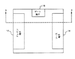
図2には、本発明の好適な実施の態様に基づく電界効果トランジスタ(FET)10のアレイ・ブロックが示されている。FETは、好ましくは1995年1月24日付けの米国特許第5384691号明細書中に記載のごとき電力用途のために特に適した金属−酸化物−半導体電界効果トランジスタ(MOSFET)である。かかるFETブロックは、たとえば通常の市販タイプのFETの1個以上から成るものである。かかるFETブロックは、1988年11月8日付けの米国特許第4783695号明細書中に記載のごとき高密度相互接続(HDI)技術を用いて製造される。FET10はドレイン端子12、ソース端子14及びゲート端子16を有するが、それらは本明細書中においてそれぞれドレイン電極、ソース電極及びゲート電極と呼ばれることもあり、またそれぞれドレイン・パッド、ソース・パッド及びゲート・パッドと呼ばれることもある。後述のごとく、複数のFET10を配列してマルチデバイス・パッケージが形成されることもあるが、かかるパッケージは外部接続用(すなわち、ゲート制御回路、電源及びドレインに対する接続用)の3つの端子を有している。これら3つの端子は、表面取付用のポスト、ワイヤ・ボンディング用のパッド、又はその他適宜の端子であり得る。
【0016】
一実施態様に従えば、図1のFETアレイ・ブロックは、ドレイン、ゲート及びソース用の結線を上側に有する自立したマルチチップ・モジュールである。接点が上側及び下側の両方にあるのではなく全ての接点が一方の側にあれば、片側パッケージング技術を有利に使用することができる。
図3には、2個以上のFET10を含むマルチデバイス高密度相互接続(HDI)パッケージ18が示されている。なお、説明の都合上、FET10は電力用FETである。図3について説明すれば、熱拡散体として役立つ銅パッド22がセラミック基板20上に取付けられている。各々のFET10は実質的に従来通りのものであって、メタライズ表面を有するN+ 型基板のドレイン層24を含んでいる。それのメタライズ表面は銅パッド22にはんだ付けされ、そしてドレイン端子12(図2)として役立つ。各々のドレイン層24上にはN- エピタキシャル層26が配置されているが、それの中央部分はP- ベース層28によって占められており、またその中にはN+ 層30が含まれている。図3に示されるごとく、層28及び30の一部分上には多結晶質シリコンのゲート層32が配置され、また層30及び32の一部分上にはN+ 拡散層34が配置されている。やはり図3に示されるごとく、層32及び34の一部分上には前記のゲート端子16に対応するゲート金属層16が配置され、また層28、30及び34の一部分上には前記のソース端子14に対応するソース金属層14が配置されている。
【0017】
一実施態様に従えば、ドレイン端子12はFET10の下部に配置することができる。すなわち、ドレイン層24のメタライズ表面が銅パッド22にはんだ付けされる結果、全てのFETのドレイン端子が銅パッド22によって相互接続される。かかる下部のドレイン端子に対しては、ドレイン端子を外部装置に対して電気的に接続するため、図4の要素48に関連して後述されるような電気的貫通部材が設けられる。別の実施態様に従えば、図3中の参照番号36によって示されるようなFET10から分離した銅ポストを使用することにより、(図2に示されるごとく)ドレイン端子12をFET10の上部に配置することもできる。かかる銅ポスト36は銅パッド22にはんだ付けされ、そして少なくとも1個のFET10の上面の位置まで上方に延びている。前記の各々のFET10がそれの下部にドレイン端子24を有し、各々のFET10の下部のドレイン端子24が下部メタライズ層22に電気的に接触している。ポスト36は前記下部メタライズ層22から延びる。
【0018】
図3にはまた、ドレイン端子12、ソース端子14及びゲート端子16をそれぞれ相互接続するための第1のメタライズ層38、第2のメタライズ層40及び第3のメタライズ層42が示されている。第1のメタライズ層38及び第2のメタライズ層40はそれぞれ0.5ミルの典型的な厚さを有する銅層から成ることが好ましいのに対し、第3のメタライズ層42は約0.5〜1.0ミルの典型的な厚さを有する銅層から成ることが好ましい。マルチデバイス・パッケージ18の総合寄生インダクタンスを低減させるため、第1のメタライズ層38及び第2のメタライズ層40は互いに平行な2つの平面内に配置されている。なお、下側のドレイン端子の場合には銅ポスト36が不要となり、そして5ミルの典型的な厚さを有する銅パッド22が第1のメタライズ層38と同じ機能を果たすことになる。
【0019】
やはり図3からわかる通り、デュポン社(E.I. DuPont de Nemours & Co.)から入手可能なカプトン(Kapton;登録商標)のごとき樹脂ベース重合体複合物から成り且つ1ミルの典型的な厚さを有するポリイミド誘電体層44により、層38、40及び42は互いに分離されている。
層38、40及び42は、関連する誘電体層44中に形成された1つ以上のスルーホール46を通して、ドレイン端子12、ソース端子14及びゲート端子16にそれぞれ接続されている。あるいはまた、誘電体層44のアブレーションによってドレイン端子12(銅ポスト36)、ソース端子14及びゲート端子16をそれぞれ露出させ、そしてそれらに対し適宜に接続を行うこともできる。図3の実施態様においては、層38は2段構造のスルーホール46を有し、層40は1段構造のスルーホール46を有し、また層42は3段構造のスルーホール46を有している。なお、図示を簡明にするため、最後のスルーホール46は図3中の右側のFET10についてのみ示してある。スルーホール46の構造は、層38、40及び42が互いに任意の位置関係を有するように選定することができる。かかるマルチデバイス高密度相互接続パッケージ18は、図4に関連して一層詳しく説明される。
【0020】
図4は、16個の電力用FET10の配列を示すものである。図示を簡明にするため、図4中にはゲート端子16に付随する第3のメタライズ層42のみが完全に示されていて、ドレイン端子12及びソース端子14にそれぞれ関連する(図3中に示された)第1のメタライズ層38及び第2のメタライズ層40は示されていない。ただし、図4中には、導電性材料から成り且つドレイン端子12及びソース端子14にそれぞれ付随する接点パッド48及び50が示されている。
【0021】
接点パッド48は図3に関連して前記に貫通部材48として記載されたものであって、適宜の手段(たとえば、はんだ付け又は直接の銅ボンディング)により銅パッド22に対して電気的に接続されている。なお、図3に関連して前記に記載した通り、銅パッド22はマルチデバイス・パッケージ18を構成する各々のFET10のドレイン端子に対して電気的に接続されている。接点パッド48は、外部装置に対するドレイン端子12の電気的接続を1箇所において可能にする。このような構造の接点パッド48に対しては、図4中に示される銅ポスト36は不要となる。
【0022】
接点パッド50が、(図3中に示された)第2のメタライズ層40及び(図4中に示されているが一層完全には図3中に示された)スルーホール46を介し、各々のFET10のソース端子に対して電気的に接続されている。接点パッド50は、外部装置に対するソース端子14の電気的接続を1箇所において可能にする。
【0023】
第3のメタライズ層42は、全てのFET10のゲート端子16を互いに並列に配置させるただ1つの連続層を与える点で有利である。更にまた、第3のメタライズ層42は第1の(ドレイン)メタライズ層38及び第2の(ソース)メタライズ層40のそれぞれに対して両者間の重なりが最小となるように配置されている。その結果、ゲート端子16(層42)とドレイン端子12(層38)との間の重なり容量が最小になると共に、ゲート端子16(層42)とソース端子14(層40)との間の重なり容量が最小になり、それはまたFET10のスイッチング速度の低下を最少限に抑える。
【0024】
図5は、図4のFETアレイ18と同様なFETアレイ52を示している。この場合には、アレイ52の一部を成すように組込まれ且つそれの中心領域に配置されたゲート駆動回路網54が追加されている点で異なっている。ゲート駆動回路網54が中心に配置されている結果、ゲート駆動回路網54を構成する4個のFETのゲート端子14に対して末端が電気的に接続されたX字形の中心部分を有する信号分配手段56によって可能となる対称的なレイアウトを利用することができる。図5にはまた、ゲート駆動回路網54のスルーホール60を介してFET10のソース端子を相互接続するメタライズ領域58も示されている。所望ならば、メタライズ領域58は接点パッド50に接続される(図3中に示された)第2のメタライズ層40の一部を成していてもよい。ゲート駆動回路網54をメタライズ層40から分離したままにしたい場合には、図3中の接点パッド50及び48に関して記載されたごとくにして、ゲート駆動回路網54のFETのソース端子用の接点パッド(図示せず)をドレイン端子用の接点パッドと共に設けることが必要である。図4及び5中のFETは、図2及び3中のFETと同じく、1つの実効ゲート抵抗を生み出すようにただ1個のゲート接点を有している。実効ゲート抵抗を更に低下させるためには、図6に関連して記載されるごとくに4個のゲート接点パッドを有するFETを使用すればよい。
【0025】
図6は、FET62の外周の四隅に配置され且つ第3のメタライズ層42によって相互接続された4個のゲート端子16A、16B、16C及び16Dを有するFET62を示している。かかるFET62はまた、第2のメタライズ層40に対して電気的に接続された接点パッドアレイ64を含んでいるが、これは図4及び5中のソース接点パッド50の代りに使用することができる。図6に示されたもののごとき第2及び第3レベルの相互接続構造物を得るためには、HDI構造物を使用するのが有利である。
【0026】
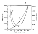
図4を参照しながら動作を説明すれば、FETアレイ18はそれを構成する個々のFET10と同じ降伏電圧及び(又は)電力レベルを有している。実際には、かかる降伏電圧は最低の降伏電圧を有するFET10によって決定される。本明細書中において、「降伏電圧」及び「電力レベル」という用語はFET10の電力スイッチング・パラメータを記述するため互換的に使用されることがある。FETアレイ18の全オン抵抗は個々のFET10のオン抵抗を並列に組合わせたものである。それ故、図4に示されるごとくに16個のFETが使用された場合には、FETアレイ18の全抵抗は1個のFET10の抵抗の16分の1に等しく、このことは伝導損失についても同様である。他方、FETアレイ18のゲート・スイッチング容量は個々のFET10の容量の16倍に等しい。しかるに、特定の用途に対しては、伝導(抵抗)損失とスイッチング(容量)損失との間に最適のバランスが得られるようにFET10の数を選定することができる。更にまた、このように数が選定可能であることはFET10の歩留りを向上させる。なぜなら、それは所望の伝導損失及びスイッチング損失を有する1個のFET10を製造することの必要性を排除するからである。FET10の数の選定によってFET10のゲート抵抗に関連する所望の伝導損失及びスイッチング損失が得られることは、図7に関連して下記に一層詳しく説明される。
【0027】
図7は、全FET電力分布をFETの面積に対してプロットした1群の曲線から成るグラフ66を示している。このグラフ66は曲線68、70及び72を含んでいて、曲線68及び70は市販のFETタイプ1RF150及び1RF230の動作応答を表わし、また曲線72は1MHzを越えるスイッチング能力を有する特定のFETの容量を表わす。図7において、X軸はFETのチップ・サイズ(ミル)を表わし、また第1のY軸は抵抗損失(ワット)を表わし、且つ第2のY軸は容量性損失(pf)を表わす。
【0028】
図7からわかる通り、最小電力損失はFETサイズの強い関数であり、またこの最小電力損失は定格電圧、スイッチング周波数及び電力レベルにも依存する。図7に示されたパラメータは、FET10又はFETアレイ18及び52がオン抵抗及びスイッチング容量に関して最適の構成を有するように選定することができる。更に詳しく述べれば、FET10は50ミル(図7のX軸の勾配)のチップ・サイズを有するように選定すればよく、次いでFET10の数は曲線68、70及び72に関する任意所望の動作領域に対応するように選定すればよい。
【0029】
FETアレイを構成するFETの数を選定し得ることの利点の1つは、大型の装置を形成し得ることである。このことは、大型のFETアレイについてばかりでなく、100KHz〜10MHzのスイッチング速度を有する上記のごときFET10に比べて比較的低いスイッチング周波数(10KHz〜150KHz)で動作するIGBTから構成されたもののような大型のMOSゲート・アレイについても言える。これらのスイッチング周波数については伝導損失が支配的になることが多いから、このようにして選定可能なアレイには利益がある。更にまた、本発明の実施はたとえば米国特許第5384691号明細書中に一層詳しく記載された利用法を有する電力用MOS−FETデバイスにも等しく適用することができる。
【0030】
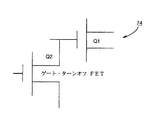
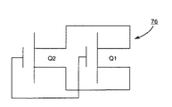
本発明のFETアレイ中には、一層良好な性能及び(又は)より多くの機能を付与するためにその他のデバイス(すなわち、ゲート駆動回路網54のFET以外のデバイス)を組込むこともできる。かかる追加のデバイスを本発明のFETアレイ中に組込むためには、追加のリードを使用するのではなく(すなわち、不都合な容量性及び誘導性負荷効果を回避しながら)、最小の容量性負荷及び最小の相互接続長さを有する前述のメタライズ層を使用することに注意されたい。かかるその他のデバイスから成るビルディング・ブロックの代表例としては、過温度モニタ、静電放電(ESD)損傷保護装置及び電流ミラー装置が挙げられる。図8乃至図11には、かかるその他のデバイスの具体例が略示されている。
【0031】
図8はゲート・ターンオフ回路74、図9は並列FET76、図10は電流ミラー78、及び図11はゲート・ドライバ回路80をそれぞれ示している。図8にはFET(Q1及びQ2)が示されているが、Q2はターンオフに際してゲート電流に対する低抵抗の流路として働くゲート・ターンオフFETとして配置されている。かかる低インピーダンスの流路は、Q2をターンオンさせる場合に重要である。図9には、図示のごとくに配置された2個のFET(Q1及びQ2)によって構成される並列回路が示されている。
【0032】
図10には、電流ミラーFETとして働くFET(Q2)を含む電流ミラー回路が示されている。電流ミラーFET(Q2)は隔離された独立のソース接点を有していて、それはたとえば図10の回路中を流れる全電流の代表サンプルを与える。かかるサンプルは制御ループの一部として使用することができる。
図11は、FET(Q2)がたとえば図5のFETアレイ46の一部を成すゲート駆動FETとして働くようなゲート駆動回路を示している。
【0033】
全ての図示されたFET配置以外にも、図4及び5のFETアレイの各々は熱拡散支持体(たとえば銅パッド22)上に配置された自給式装置として取扱うこともできる。それの最も簡単な形態である図2及び3のFET10は(ゲート、ソース及びドレイン端子を有する)三端子デバイスであるが、一連のスルーホールを用いて図3に略示されるごとくに全ての接点を同じ表面に移動させることによってそれら3個の端子の全てを同一平面上に配置することもできる。これは、銅パッド22がたとえば約40ミルの厚さを有する場合に特に重要である。
【0034】
本発明は、アレイ状に配列された1個以上のFETから成るFETアレイにおいて、全てのFETのゲート、ソース及びドレイン端子を3つのメタライズ層により電気的に相互接続して成るFETアレイを提供するという点で有利である。かかるFETアレイは、電力レベルが選定可能であるという要求を満たすため、所望のオン抵抗及びスイッチング容量を生み出すように選定することができる。
【0035】
本発明はまた、幾つかの製造上の利点をも有する。第一に、ただ一つのサイズのFETを製造すれば事足りるのであって、これらのFETの数を選定することによって特定の電力レベルに対する所望の動作応答を得ることができる。第二に、ビルディング・ブロック(ただ一つのサイズのFET)を用いて大きなダイを形成することは歩留りを向上させる。
【0036】
以上、特定の実施の態様に関連して本発明を説明したが、それ以外にも数多くの変更態様が可能であることは当業者にとって自明であろう。それ故、本発明の真の精神に反しない限り、特許請求の範囲はかかる変更態様の全てを包括するものであることを理解すべきである。
【図面の簡単な説明】
【図1】ポリシリコン抵抗器−MOSゲート回路網によって表わされる多結晶質ゲート電極を使用した従来の電界効果トランジスタを示す回路図である。
【図2】本発明の実施の一態様に基づく電界効果トランジスタを示す略図である。
【図3】図2中の線3−3に沿って取った、図2のFETの断面図である。
【図4】本発明の好適な実施態様のFETアレイを示す平面図である。
【図5】本発明の別の好適な実施態様のFETアレイを示す平面図である。
【図6】本発明の別の好適な実施態様のFETアレイを示す平面図である。
【図7】本発明の動作に係わる性能曲線を示すグラフである。
【図8】本発明のFETアレイ中に組込むことのできるデバイスの模式図である。
【図9】本発明のFETアレイ中に組込むことのできる別のデバイスの模式図である。
【図10】本発明のFETアレイ中に組込むことのできる別のデバイスの模式図である。
【図11】本発明のFETアレイ中に組込むことのできる別のデバイスの模式図である。
【符号の説明】
10 電界効果トランジスタ(FET)
12 ドレイン端子
14 ソース端子
16 ゲート端子
18 パッケージ(FETアレイ)
20 セラミック基板
22 銅パッド
36 銅ポスト
38 第1のメタライズ層
40 第2のメタライズ層
42 第3のメタライズ層
46 スルーホール
48 接点パッド
50 接点パッド
52 FETアレイ
54 ゲート・ドライバ回路網
56 信号分配手段
58 メタライズ領域[0001]
BACKGROUND OF THE INVENTION
The present invention relates to a field effect transistor.
[0002]
[Prior art]
Field effect transistors (FETs), particularly metal-oxide-semiconductor field effect transistors (MOSFETs), have inherent switching capabilities at high frequencies (turn-on and turn-off within 10 nanoseconds), which makes them suitable for various power switching applications. It has become increasingly popular for use. Because of this high switching capability, power circuits using FET devices have been improved for operation at increasingly higher frequencies. The main goal of pursuing operation at high frequencies (f) is to reduce the size (proportional to 1 / f) of passive components such as transformers and filter capacitors that can occupy a significant portion of the device volume. It is to reduce. If power semiconductors (FETs) can be switched at high frequencies, magnetic devices and energy storage (CV)2It is possible to reduce the filter to 1 / f (because it is proportional to f). For operation up to 1 MHz, FET performance is satisfactory. However, as the frequency increases to over 10 MHz, its switching efficiency and safe operating area (SOA) are limited by several factors. The most serious limitation relates to the gate arrangement of FET arrays that are integrated electrically in parallel on a silicon wafer or die. In most power FETs, the gate electrode is made of a polycrystalline silicon material having a resistivity that is an order of magnitude higher than other metals (eg, aluminum). The reason for choosing the use of polycrystalline silicon is mainly because of its superior properties including the ability to withstand high temperatures and the ability to provide a well-controlled electrical interface to silicon oxide.
[0003]
Although polycrystalline silicon has advantageous properties, the use of polycrystalline silicon as the gate electrode has several drawbacks. These drawbacks will be described with reference to FIG. In FIG. 1, a plurality of polycrystalline gate electrodes comprise a plurality of polysilicon resistor-MOS gate networks 102.1, 1022, 102Three... 102NIndicated by. As can be seen from FIG. 1, typically the
[0004]
As a result, at turn-on, the polysilicon resistor-
[0005]
To achieve faster switching speeds, it is necessary to minimize the capacitive load and interconnect length associated with the interconnection from one FET to another in the array, thereby keeping the interconnect inductance low It is. Capacitive loads and inductive loads tend to slow down signal transmission, so that high speeds cannot be maintained when communicating between FETs. This is not a problem for adjacent FETs, but is a problem for other FETs. The configuration of FIG. 1 is subject to such restrictions.
[0006]
Furthermore, when FETs used for high power switching applications are excited by a sine wave, the gate resistance seen when using a polycrystalline silicon gate electrode also affects switching losses. For such excitation, the switching loss of the gate is proportional to the gate resistance of the power FET and other resistances in the gate drive circuit. Other resistors in the conventional gate drive circuit include interconnect resistors arranged in series between the drive device and the main power FET driven by the drive device. In order to perform switching at a high frequency, it is known to use a sinusoidal (resonant) driving technique so that the switching loss is proportional to the gate resistance rather than the frequency. However, these techniques require the use of devices external to the FET chip, which increases the inductance of the interconnect leads and thus reduces the switching speed performance of the FET.
[0007]
The efficiency of the FET is affected by factors that contribute to conduction and switching. In general, conduction loss is inversely proportional to the size (or resistance) of the power FET die, while gate switching loss is directly proportional to size (or gate capacitance). Therefore, it is a difficult task to balance conduction loss and switching loss. In particular, as the switching frequency increases, the use of larger devices to reduce conduction losses will have the opposite result due to the increase in switching losses proportional to the switching frequency. In any power circuit operating at a given switching frequency, there is an optimal FET size (resistance and capacitance) that minimizes power loss. However, as a practical matter, such an optimal FET size is not always easily achieved. This is because, for economic reasons, vendors do not provide a number of commercially available FET dies that each have a predetermined breakdown voltage and power level (which determines the size of the FET die).
[0008]
As such, it would be desirable to provide FETs and FET arrays that can be easily optimized for any given power level. Furthermore, it is also desirable to optimize FETs and FET arrays as described above using a limited inventory of commonly available FET dies.
Recently, manufacturers have addressed the non-uniform gate signal distribution problem described in connection with FIG. 1 in various ways. One example is to incorporate an extra metallization level gate runner, thereby reducing the gate runner resistance. For relatively high voltage devices, it is customary to achieve a large number of aluminum gate runners, but for relatively low voltage devices with limited topologies, such a large number of gate runners are achieved. It is impossible to do. Although reducing the gate runner resistance for relatively high voltage devices has an advantageous effect, the extra metallization level increases the burden of the device manufacturing process.
[0009]
Furthermore, attempts have been made to protect the device from slower switching speeds by incorporating additional circuitry such as current mirrors in the device package, but such additional circuitry represents an increase in cost.
High density interconnect (HDI) structures for integrated circuit packaging, such as those described in more detail in U.S. Pat. Nos. 4,783,695 and 5,384,691, for example, present several drawbacks related to device interconnection. Eliminate. The metallization layer used in HDI packaging is a drawback caused by using leads for chip-to-chip and intra-chip connections as a result of providing excellent conductivity for interconnection between individual chips. Substantially reduce unnecessary self-inductance and capacitive load. Therefore, it is desirable to utilize HDI technology to release commercially available FET devices from switching speed and performance constraints.
[0010]
[Problems to be solved by the invention]
From the above, it is an FET array freed from the restriction that the circuit performance is degraded due to the limited availability of various commercially available FETs, in order to reduce the effective resistance of the polycrystalline silicon gate electrode It would be desirable to provide an FET array that uses high density interconnect (HDI) technology to reduce the capacitive and inductive loading effects of the interconnect that limit the switching capability of the FET array.
[0011]
[Means for Solving the Problems]
The present invention increases the high resistance of a polycrystalline silicon gate electrode by providing three or more metallization layers for the source terminal, drain terminal and gate terminal of one or more commercial field effect transistors (FETs). A package is formed that compensates and provides a high level of circuit performance with an optimal balance between conduction (resistance) loss and switching (capacitance) loss.
[0012]
That is, the present invention includes one or more FETs each having a gate terminal, a source terminal, and a drain terminal, each gate terminal having a predetermined resistance, and a predetermined resistance between the gate terminal and the source terminal. The present invention relates to an (FET) package in which there is an overlap capacitance of. In such a FET package, first, second and third metallization layers are provided. The first metallization layer constitutes a support on which each FET is mounted and is electrically interconnected to the drain terminal of each FET. The second metallized layer is disposed in parallel with the first metallized layer and is formed so as to reduce the overlapping capacitance between the gate terminal and the source terminal. The second metallization layer is electrically connected to the source terminal of each FET by a plurality of through holes. The third metallization layer forms a gate runner, is electrically interconnected to the gate terminal of each FET, and is formed to reduce the gate resistance of one or more FETs.
[0013]
Additional semiconductor devices can be incorporated into the FET package using additional terminals interconnected through a metallization layer. Thereby, additional components such as a gate drive, an overtemperature monitor and a current mirror device can be added.
[0014]
DETAILED DESCRIPTION OF THE INVENTION
While the features of the invention believed to be novel are set forth in the appended claims, the construction and implementation of the invention and its additional objects and advantages will be described in the following with reference to the accompanying drawings. It should be understood most clearly by consideration. Note that the same constituent elements are denoted by the same numbers in all the drawings.
[0015]
FIG. 2 shows an array block of field effect transistors (FETs) 10 according to a preferred embodiment of the present invention. The FET is preferably a metal-oxide-semiconductor field effect transistor (MOSFET) that is particularly suitable for power applications such as those described in US Pat. No. 5,384,691, dated January 24, 1995. Such a FET block comprises, for example, one or more conventional commercially available FETs. Such FET blocks are manufactured using high density interconnect (HDI) technology such as that described in US Pat. No. 4,783,695, issued Nov. 8, 1988. The
[0016]
According to one embodiment, the FET array block of FIG. 1 is a free standing multichip module with drain, gate and source connections on the top side. If all contacts are on one side rather than being on both the upper and lower sides, a one-side packaging technique can be advantageously used.
FIG. 3 shows a multi-device high density interconnect (HDI)
[0017]
According to one embodiment, the drain terminal 12 can be located below the
[0018]
FIG. 3 also shows a
[0019]
As can also be seen from FIG. 3, it consists of a resin-based polymer composite such as Kapton® available from EI DuPont de Nemours & Co. and has a typical thickness of 1 mil. The
[0020]
FIG. 4 shows an arrangement of 16
[0021]
[0022]
Contact
[0023]
The
[0024]
FIG. 5 shows an
[0025]
FIG. 6 shows an FET 62 having four
[0026]
In operation, with reference to FIG. 4, the
[0027]
FIG. 7 shows a
[0028]
As can be seen from FIG. 7, the minimum power loss is a strong function of the FET size, and this minimum power loss also depends on the rated voltage, switching frequency and power level. The parameters shown in FIG. 7 can be selected so that
[0029]
One advantage of being able to select the number of FETs that make up the FET array is that large devices can be formed. This is not only for large FET arrays, but also for large ones such as those composed of IGBTs that operate at a relatively low switching frequency (10 KHz to 150 KHz) compared to
[0030]
Other devices (i.e., devices other than FETs in the gate drive network 54) can be incorporated into the FET array of the present invention to provide better performance and / or more functionality. In order to incorporate such additional devices into the FET array of the present invention, rather than using additional leads (ie, avoiding adverse capacitive and inductive loading effects), the minimum capacitive load and Note the use of the aforementioned metallization layer with the minimum interconnect length. Typical examples of such other building blocks include over-temperature monitors, electrostatic discharge (ESD) damage protection devices, and current mirror devices. Specific examples of such other devices are schematically shown in FIGS.
[0031]
8 shows a gate turn-
[0032]
FIG. 10 shows a current mirror circuit including an FET (Q2) that functions as a current mirror FET. The current mirror FET (Q2) has an isolated independent source contact, which provides a representative sample of the total current flowing through, for example, the circuit of FIG. Such a sample can be used as part of a control loop.
FIG. 11 shows a gate drive circuit in which FET (Q2) acts as a gate drive FET that forms part of, for example,
[0033]
In addition to all the illustrated FET arrangements, each of the FET arrays of FIGS. 4 and 5 can also be treated as a self-contained device placed on a thermal diffusion support (eg, copper pad 22). In its simplest form, the
[0034]
The present invention provides an FET array comprising one or more FETs arranged in an array, wherein the gate, source and drain terminals of all FETs are electrically interconnected by three metallization layers. This is advantageous. Such FET arrays can be selected to produce the desired on-resistance and switching capacitance to meet the requirement that the power level be selectable.
[0035]
The present invention also has several manufacturing advantages. First, it is sufficient to produce only one size FET, and by selecting the number of these FETs, a desired operating response for a particular power level can be obtained. Secondly, using a building block (only one size FET) to form a large die improves yield.
[0036]
While the invention has been described with reference to specific embodiments, it will be apparent to those skilled in the art that many other modifications are possible. Therefore, it is to be understood that the claims are intended to cover all such modifications as long as they do not depart from the true spirit of the invention.
[Brief description of the drawings]
FIG. 1 is a circuit diagram illustrating a conventional field effect transistor using a polycrystalline gate electrode represented by a polysilicon resistor-MOS gate network.
FIG. 2 is a schematic diagram illustrating a field effect transistor according to an embodiment of the present invention.
3 is a cross-sectional view of the FET of FIG. 2 taken along line 3-3 in FIG.
FIG. 4 is a plan view showing an FET array according to a preferred embodiment of the present invention.
FIG. 5 is a plan view showing an FET array according to another preferred embodiment of the present invention.
FIG. 6 is a plan view showing an FET array according to another preferred embodiment of the present invention.
FIG. 7 is a graph showing a performance curve related to the operation of the present invention.
FIG. 8 is a schematic diagram of a device that can be incorporated into the FET array of the present invention.
FIG. 9 is a schematic diagram of another device that can be incorporated into the FET array of the present invention.
FIG. 10 is a schematic diagram of another device that can be incorporated into the FET array of the present invention.
FIG. 11 is a schematic diagram of another device that can be incorporated into the FET array of the present invention.
[Explanation of symbols]
10 Field Effect Transistor (FET)
12 Drain terminal
14 Source terminal
16 Gate terminal
18 Package (FET array)
20 Ceramic substrate
22 Copper pads
36 Copper post
38 First metallization layer
40 Second metallization layer
42 Third metallization layer
46 Through hole
48 contact pads
50 contact pads
52 FET array
54 Gate driver network
56 Signal distribution means
58 Metallized area
Claims (9)
前記2個以上のFETの各々のドレイン端子に対して電気的に相互接続されている第1のメタライズ層、
前記2個以上のFETの各々のソース端子に対して電気的に相互接続されている第2のメタライズ層、並びに
前記2個以上のFETの各々のゲート端子に対して電気的に相互接続されており、ゲート・ランナを構成する第3のメタライズ層を含み、
前記2個以上のFETの各々のドレイン端子が前記第1のメタライズ層と電気的に接続された下部メタライズ層の上に取付けられ、
前記ゲート・ランナが前記第1及び第2のメタライズ層と平行に配置され、
前記各々のFETのドレイン端子とソース端子とが、ゲート端子に対して重なり容量を有するように前記ゲート・ランナが前記第1及び第2のメタライズ層と重なる部分を有すること、を特徴とする電界効果トランジスタ・パッケージ。Each includes a gate terminal, a source terminal, and a drain terminal, and includes two or more field effect transistors (FETs) mounted on the substrate, each gate terminal having a resistance and a drain terminal of each FET And a field effect transistor package comprising a field effect transistor array such that the source terminal overlaps the gate terminal and has a capacitance.
A first metallization layer electrically interconnected to a drain terminal of each of the two or more FETs;
A second metallization layer electrically interconnected to the source terminal of each of the two or more FETs, and electrically interconnected to the gate terminal of each of the two or more FETs. Including a third metallization layer constituting the gate runner,
A drain terminal of each of the two or more FETs is mounted on a lower metallization layer electrically connected to the first metallization layer ;
The gate runner is disposed in parallel with the first and second metallization layers;
The electric field characterized in that the gate runner has a portion overlapping the first and second metallization layers so that the drain terminal and the source terminal of each FET have an overlapping capacitance with respect to the gate terminal. Effect transistor package.
Applications Claiming Priority (2)
| Application Number | Priority Date | Filing Date | Title |
|---|---|---|---|
| US09/024,485 US5959357A (en) | 1998-02-17 | 1998-02-17 | Fet array for operation at different power levels |
| US09/024485 | 1998-02-17 |
Publications (2)
| Publication Number | Publication Date |
|---|---|
| JPH11274370A JPH11274370A (en) | 1999-10-08 |
| JP4424698B2 true JP4424698B2 (en) | 2010-03-03 |
Family
ID=21820831
Family Applications (1)
| Application Number | Title | Priority Date | Filing Date |
|---|---|---|---|
| JP02679799A Expired - Fee Related JP4424698B2 (en) | 1998-02-17 | 1999-02-04 | Field effect transistor package |
Country Status (3)
| Country | Link |
|---|---|
| US (1) | US5959357A (en) |
| EP (1) | EP0938138A3 (en) |
| JP (1) | JP4424698B2 (en) |
Families Citing this family (37)
| Publication number | Priority date | Publication date | Assignee | Title |
|---|---|---|---|---|
| KR100230428B1 (en) * | 1997-06-24 | 1999-11-15 | 윤종용 | Semiconductor device comprising a multi-conductive pad and method for manufacturing the same |
| US6057779A (en) | 1997-08-14 | 2000-05-02 | Micron Technology, Inc. | Method of controlling access to a movable container and to a compartment of a vehicle, and a secure cargo transportation system |
| US6356535B1 (en) * | 1998-02-04 | 2002-03-12 | Micron Technology, Inc. | Communication systems and methods of communicating |
| US6413576B1 (en) * | 1998-10-05 | 2002-07-02 | Kulicke & Soffa Investments, Inc. | Semiconductor copper bond pad surface protection |
| US6965165B2 (en) | 1998-12-21 | 2005-11-15 | Mou-Shiung Lin | Top layers of metal for high performance IC's |
| US6303423B1 (en) * | 1998-12-21 | 2001-10-16 | Megic Corporation | Method for forming high performance system-on-chip using post passivation process |
| US6936531B2 (en) | 1998-12-21 | 2005-08-30 | Megic Corporation | Process of fabricating a chip structure |
| US10973397B2 (en) | 1999-03-01 | 2021-04-13 | West View Research, Llc | Computerized information collection and processing apparatus |
| US8636648B2 (en) | 1999-03-01 | 2014-01-28 | West View Research, Llc | Endoscopic smart probe |
| JP4094174B2 (en) * | 1999-06-04 | 2008-06-04 | 株式会社ルネサステクノロジ | Manufacturing method of semiconductor device |
| US8065155B1 (en) | 1999-06-10 | 2011-11-22 | Gazdzinski Robert F | Adaptive advertising apparatus and methods |
| US7710273B2 (en) * | 1999-09-02 | 2010-05-04 | Round Rock Research, Llc | Remote communication devices, radio frequency identification devices, wireless communication systems, wireless communication methods, radio frequency identification device communication methods, and methods of forming a remote communication device |
| US20020020898A1 (en) | 2000-08-16 | 2002-02-21 | Vu Quat T. | Microelectronic substrates with integrated devices |
| US6713859B1 (en) | 2000-09-13 | 2004-03-30 | Intel Corporation | Direct build-up layer on an encapsulated die package having a moisture barrier structure |
| US6818545B2 (en) * | 2001-03-05 | 2004-11-16 | Megic Corporation | Low fabrication cost, fine pitch and high reliability solder bump |
| US7498196B2 (en) | 2001-03-30 | 2009-03-03 | Megica Corporation | Structure and manufacturing method of chip scale package |
| US7932603B2 (en) | 2001-12-13 | 2011-04-26 | Megica Corporation | Chip structure and process for forming the same |
| TW503496B (en) | 2001-12-31 | 2002-09-21 | Megic Corp | Chip packaging structure and manufacturing process of the same |
| US6673698B1 (en) | 2002-01-19 | 2004-01-06 | Megic Corporation | Thin film semiconductor package utilizing a glass substrate with composite polymer/metal interconnect layers |
| TW584950B (en) | 2001-12-31 | 2004-04-21 | Megic Corp | Chip packaging structure and process thereof |
| TW544882B (en) | 2001-12-31 | 2003-08-01 | Megic Corp | Chip package structure and process thereof |
| JP3616605B2 (en) * | 2002-04-03 | 2005-02-02 | 沖電気工業株式会社 | Semiconductor device |
| CN100403537C (en) * | 2002-06-13 | 2008-07-16 | 松下电器产业株式会社 | Semiconductor device and its manufacturing method |
| US7119437B2 (en) * | 2002-12-26 | 2006-10-10 | Yamaha Hatsudoki Kabushiki Kaisha | Electronic substrate, power module and motor driver |
| US7427024B1 (en) | 2003-12-17 | 2008-09-23 | Gazdzinski Mark J | Chattel management apparatus and methods |
| DE102004019447A1 (en) * | 2004-04-19 | 2005-11-10 | Siemens Ag | Device, in particular intelligent power module, with planar connection technology |
| US7560808B2 (en) * | 2005-10-19 | 2009-07-14 | Texas Instruments Incorporated | Chip scale power LDMOS device |
| US20090015407A1 (en) * | 2007-07-13 | 2009-01-15 | Micron Technology, Inc. | Rifid tags and methods of designing rfid tags |
| US7777630B2 (en) * | 2007-07-26 | 2010-08-17 | Round Rock Research, Llc | Methods and systems of RFID tags using RFID circuits and antennas having unmatched frequency ranges |
| US8179232B2 (en) * | 2008-05-05 | 2012-05-15 | Round Rock Research, Llc | RFID interrogator with adjustable signal characteristics |
| US7852221B2 (en) * | 2008-05-08 | 2010-12-14 | Round Rock Research, Llc | RFID devices using RFID circuits and antennas having unmatched frequency ranges |
| US8712334B2 (en) | 2008-05-20 | 2014-04-29 | Micron Technology, Inc. | RFID device using single antenna for multiple resonant frequency ranges |
| US8053898B2 (en) * | 2009-10-05 | 2011-11-08 | Samsung Electronics Co., Ltd. | Connection for off-chip electrostatic discharge protection |
| US8847293B2 (en) * | 2012-03-02 | 2014-09-30 | Taiwan Semiconductor Manufacturing Company, Ltd. | Gate structure for semiconductor device |
| US9337163B2 (en) * | 2012-11-13 | 2016-05-10 | General Electric Company | Low profile surface mount package with isolated tab |
| US9006584B2 (en) * | 2013-08-06 | 2015-04-14 | Texas Instruments Incorporated | High voltage polymer dielectric capacitor isolation device |
| US9899484B1 (en) * | 2016-12-30 | 2018-02-20 | Texas Instruments Incorporated | Transistor with source field plates under gate runner layers |
Family Cites Families (11)
| Publication number | Priority date | Publication date | Assignee | Title |
|---|---|---|---|---|
| US4182023A (en) * | 1977-10-21 | 1980-01-08 | Ncr Corporation | Process for minimum overlap silicon gate devices |
| US4198250A (en) * | 1979-02-05 | 1980-04-15 | Intel Corporation | Shadow masking process for forming source and drain regions for field-effect transistors and like regions |
| US4343078A (en) * | 1979-03-05 | 1982-08-10 | Nippon Electric Co., Ltd. | IGFET Forming method |
| US4471524A (en) * | 1982-06-01 | 1984-09-18 | At&T Bell Laboratories | Method for manufacturing an insulated gate field effect transistor device |
| CA1198226A (en) * | 1982-06-01 | 1985-12-17 | Eliezer Kinsbron | Method for manufacturing a semiconductor device |
| JPH06101652B2 (en) * | 1987-02-12 | 1994-12-12 | 三菱電機株式会社 | Bias circuit |
| US4783695A (en) * | 1986-09-26 | 1988-11-08 | General Electric Company | Multichip integrated circuit packaging configuration and method |
| US5384691A (en) * | 1993-01-08 | 1995-01-24 | General Electric Company | High density interconnect multi-chip modules including embedded distributed power supply elements |
| US5696403A (en) * | 1993-10-25 | 1997-12-09 | Lsi Logic Corporation | System having input-output drive reduction |
| US5455442A (en) * | 1993-11-17 | 1995-10-03 | Harris Corporation | COMFET switch and method |
| US5498556A (en) * | 1995-01-10 | 1996-03-12 | United Microelectronics Corp. | Metal-oxide-semiconductor field-effect transistor and its method of fabrication |
-
1998
- 1998-02-17 US US09/024,485 patent/US5959357A/en not_active Expired - Lifetime
-
1999
- 1999-02-04 JP JP02679799A patent/JP4424698B2/en not_active Expired - Fee Related
- 1999-02-17 EP EP99301160A patent/EP0938138A3/en not_active Ceased
Also Published As
| Publication number | Publication date |
|---|---|
| JPH11274370A (en) | 1999-10-08 |
| EP0938138A2 (en) | 1999-08-25 |
| EP0938138A3 (en) | 2003-08-20 |
| US5959357A (en) | 1999-09-28 |
Similar Documents
| Publication | Publication Date | Title |
|---|---|---|
| JP4424698B2 (en) | Field effect transistor package | |
| JP4192396B2 (en) | Semiconductor switching module and semiconductor device using the same | |
| KR100695031B1 (en) | Electronic semiconductor module | |
| Fisher et al. | High frequency, low cost, power packaging using thin film power overlay technology | |
| US10665398B1 (en) | Direct current solid-state switch | |
| EP2899756A1 (en) | Semiconductor device | |
| US6900537B2 (en) | High power silicon carbide and silicon semiconductor device package | |
| US7019362B2 (en) | Power MOSFET with reduced dgate resistance | |
| CN210349834U (en) | Double-side radiating power device module | |
| US8030758B2 (en) | Semiconductor module and method for fabricating semiconductor module | |
| US5366932A (en) | Semi-conductor chip packaging method and semi-conductor chip having interdigitated gate runners with gate bonding pads | |
| US10573585B2 (en) | Power converter having a conductive clip | |
| US7042730B2 (en) | Non-isolated heatsink(s) for power modules | |
| US11133303B2 (en) | Semiconductor device and semiconductor arrangement comprising semiconductor devices | |
| US11527456B2 (en) | Power module with organic layers | |
| JP3525823B2 (en) | Mounting structure of complementary IGBT | |
| KR20210146809A (en) | Power module | |
| KR20220004442A (en) | Power module | |
| JPH08340082A (en) | Power semiconductor device | |
| KR20220004437A (en) | Power module | |
| KR20220010180A (en) | Power module | |
| EP3660896A1 (en) | Semiconductor arrangement | |
| EP3376538B1 (en) | Semiconductor arrangement with controllable semiconductor elements | |
| CN113748509B (en) | Semiconductor device with a semiconductor device having a plurality of semiconductor chips | |
| US20230052830A1 (en) | Power circuit module |
Legal Events
| Date | Code | Title | Description |
|---|---|---|---|
| A621 | Written request for application examination |
Free format text: JAPANESE INTERMEDIATE CODE: A621 Effective date: 20060201 |
|
| A521 | Request for written amendment filed |
Free format text: JAPANESE INTERMEDIATE CODE: A523 Effective date: 20080602 |
|
| A977 | Report on retrieval |
Free format text: JAPANESE INTERMEDIATE CODE: A971007 Effective date: 20081226 |
|
| A131 | Notification of reasons for refusal |
Free format text: JAPANESE INTERMEDIATE CODE: A131 Effective date: 20090113 |
|
| A521 | Request for written amendment filed |
Free format text: JAPANESE INTERMEDIATE CODE: A523 Effective date: 20090223 |
|
| RD02 | Notification of acceptance of power of attorney |
Free format text: JAPANESE INTERMEDIATE CODE: A7422 Effective date: 20090401 |
|
| RD04 | Notification of resignation of power of attorney |
Free format text: JAPANESE INTERMEDIATE CODE: A7424 Effective date: 20090401 |
|
| A131 | Notification of reasons for refusal |
Free format text: JAPANESE INTERMEDIATE CODE: A131 Effective date: 20090915 |
|
| A521 | Request for written amendment filed |
Free format text: JAPANESE INTERMEDIATE CODE: A523 Effective date: 20091008 |
|
| TRDD | Decision of grant or rejection written | ||
| A01 | Written decision to grant a patent or to grant a registration (utility model) |
Free format text: JAPANESE INTERMEDIATE CODE: A01 Effective date: 20091117 |
|
| A01 | Written decision to grant a patent or to grant a registration (utility model) |
Free format text: JAPANESE INTERMEDIATE CODE: A01 |
|
| A61 | First payment of annual fees (during grant procedure) |
Free format text: JAPANESE INTERMEDIATE CODE: A61 Effective date: 20091207 |
|
| R150 | Certificate of patent or registration of utility model |
Free format text: JAPANESE INTERMEDIATE CODE: R150 |
|
| FPAY | Renewal fee payment (event date is renewal date of database) |
Free format text: PAYMENT UNTIL: 20121218 Year of fee payment: 3 |
|
| LAPS | Cancellation because of no payment of annual fees |