JP4422851B2 - Coordinate input apparatus and method - Google Patents
Coordinate input apparatus and method Download PDFInfo
- Publication number
- JP4422851B2 JP4422851B2 JP2000062272A JP2000062272A JP4422851B2 JP 4422851 B2 JP4422851 B2 JP 4422851B2 JP 2000062272 A JP2000062272 A JP 2000062272A JP 2000062272 A JP2000062272 A JP 2000062272A JP 4422851 B2 JP4422851 B2 JP 4422851B2
- Authority
- JP
- Japan
- Prior art keywords
- photoelectric conversion
- conversion element
- coordinate
- output
- period
- Prior art date
- Legal status (The legal status is an assumption and is not a legal conclusion. Google has not performed a legal analysis and makes no representation as to the accuracy of the status listed.)
- Expired - Fee Related
Links
Images


Classifications
-
- G—PHYSICS
- G06—COMPUTING; CALCULATING OR COUNTING
- G06F—ELECTRIC DIGITAL DATA PROCESSING
- G06F3/00—Input arrangements for transferring data to be processed into a form capable of being handled by the computer; Output arrangements for transferring data from processing unit to output unit, e.g. interface arrangements
- G06F3/01—Input arrangements or combined input and output arrangements for interaction between user and computer
- G06F3/03—Arrangements for converting the position or the displacement of a member into a coded form
- G06F3/041—Digitisers, e.g. for touch screens or touch pads, characterised by the transducing means
- G06F3/042—Digitisers, e.g. for touch screens or touch pads, characterised by the transducing means by opto-electronic means
- G06F3/0425—Digitisers, e.g. for touch screens or touch pads, characterised by the transducing means by opto-electronic means using a single imaging device like a video camera for tracking the absolute position of a single or a plurality of objects with respect to an imaged reference surface, e.g. video camera imaging a display or a projection screen, a table or a wall surface, on which a computer generated image is displayed or projected
-
- G—PHYSICS
- G06—COMPUTING; CALCULATING OR COUNTING
- G06F—ELECTRIC DIGITAL DATA PROCESSING
- G06F3/00—Input arrangements for transferring data to be processed into a form capable of being handled by the computer; Output arrangements for transferring data from processing unit to output unit, e.g. interface arrangements
- G06F3/01—Input arrangements or combined input and output arrangements for interaction between user and computer
- G06F3/03—Arrangements for converting the position or the displacement of a member into a coded form
- G06F3/033—Pointing devices displaced or positioned by the user, e.g. mice, trackballs, pens or joysticks; Accessories therefor
- G06F3/038—Control and interface arrangements therefor, e.g. drivers or device-embedded control circuitry
- G06F3/0386—Control and interface arrangements therefor, e.g. drivers or device-embedded control circuitry for light pen
Description
【0001】
【発明の属する技術分野】
本発明は、例えば座標のような位置情報を入力し得る、特に大型表示システムに好適な方法及び装置に関する。より詳しくは、本発明は座標情報のような、表示画面上でオペレータにより指示された位置を表す位置情報を入力する装置及び方法に関するものである。オペレータは指示具を用いて位置の指示を行うことができる。その入力された位置情報は外部接続されたコンピュータを制御したり、文字や図形などを書き込む等の処理に用いられ得る。
【0002】
【従来の技術】
従来の座標入力装置としては、CCDエリアセンサやリニアセンサを用いて画面上の光スポットを撮像し、重心座標あるいはパターンマッチングを用いるなどの画像処理を行って座標値を演算して出力するものがあった。また、座標入力装置として、PSD(Position Sensitive Device)と呼ばれる位置検出素子(スポットの位置に対応した出力電圧が得られるアナログデバイス)を用いるものもある。
【0003】
例えば、特公平7−76902号公報には、可視光の平行ビームによる光スポットをビデオカメラで撮像して座標を検出し、同時に赤外拡散光で制御信号を送受する装置が開示されている。また、特開平6−274266号公報には、リニアCCDセンサと特殊な光学マスクを用いて座標検出を行う装置が開示されている。一方、日本国特許第2503182号には、PSDを用いた装置について、その構成と出力座標の補正方法が開示されている。
【0004】
【発明が解決しようとする課題】
近年、大画面ディスプレイの画面の明るさが改善され、明るく照明された環境においても十分使用できるようになってきており、その需要が拡大されつつある。このような環境では、座標入力装置は、そのような大画面ディスプレイと組み合わせて使用できるように、外乱光に対する耐性が望まれている。また、近年、無線通信手段として、赤外線を利用する機器が増加しており、赤外、可視光ともに外乱光は、増加傾向にあるため、外乱光に対する耐性は装置の重要な特性の一つとなる。
【0005】
しかしながら、前記特公平7−76902号公報及び前記特開平6−274266号公報にも開示されているように、従来のCCDセンサを用いる装置においては、光学フィルタでしか外乱光を抑制することができない。これに対して、前記特許第2503182号に開示されているPSDを用いる装置においては、光強度を周波数変調し、この変調波を同期検波することにより、外乱光の影響を抑制している。光学フィルタと併用した装置は外乱光に対しては強い特性を持ち得る。
【0006】
また、大画面ディスプレイの明るさの改善と高解像度化が進められている。このため、座標入力装置の分解能も向上させる必要があるが、外乱光に強いPSDを用いた装置ではこの点において問題がある。すなわち、センサ出力電圧のダイナミックレンジが入力範囲にそのまま対応しているため、例えば1mmの分解能或いは解像度を得る為には少なくとも60dB以上のS/N比が必要になる。特許第2503182号で開示されているように、直線性誤差のデジタル補正が必須であるため、高精度なアナログ回路と、多ビットのAD変換器と演算回路とが必要になる。さらに、センサ出力信号のS/N比は光量と光スポットのシャープさとに依存するため、外乱光の抑圧だけでなく、光スポットを作るための明るく高精度な光学系も必要になる。このようなことから、装置は非常に高価で、大型なものになってしまう。
【0007】
さらに、CCDセンサを用いて分解能を高める為に、前記特公平7−76902号公報では、複数台のビデオカメラを同時に使用する方法が開示されているが、この方法は装置を大型化し、高価にすることは明らかである。また、一台で画素数の多いビデオカメラを使用した場合には、複数のカメラを用いるよりもさらに装置が大型化し、高価となる。また、実際の画素数よりも高い分解能を画像処理によってリアルタイムで実現させるには、膨大な画像データの高速処理が必要となり、装置が大型化し、高価になる。
【0008】
また、前記特開平6−274266号公報では、特殊な光学マスクと信号処理とによって高分解能を得ることについて開示している。外乱光が小さくかつ良好なS/N比が確保できれば高分解能化は可能である。しかし実際には、リニアセンサの結像は線であって面内で外乱光との分離ができないため、結像が点になるエリアセンサに比べて外乱光の影響を受けやすい。この為、このような装置は外乱光の少ない特殊な環境においてのみしか使用され得ない。
【0009】
また一般にCCD等の光学素子は、半導体プロセスにより量産されるが、光−電気変換効率等その諸特性は、製造環境、製造条件、製造ロット等に従って大きく変動する。例えば部品公差として約±30%の光−電気変換効率の差が存在する。電源電圧5VでCCDが動作する時に、暗時のCCD出力電圧の代表値は約1.5Vであり、部品公差を考慮すればその値は一般的に約1.0〜2.0V(約±30%)のバラツキを有する。従って、その出力を固定の閾値電圧と比較することにより光出力が得られていると判定する場合には、その閾値は2.0V以上に設定されなければならないが、低いレベルの光しか到達しない構成(即ちCCD出力が小さい)においては、耐性の限界にある素子は満足な判定が不可能となり、歩留まりが低下する。前述のような個々のCCDでの閾値の調整は光の感度を向上させるが、調整組み立てが必要となるため、組み立て工数が増大し、コストアップの要因となる。
【0010】
本発明は上記の従来技術の問題に鑑みてなされたものであり、その目的の一つは外乱光影響を抑制し、高分解能で高性能な座標入力装置及び方法を提供することにある。
【0011】
また、本発明の他の目的は、小型で、低コストな座標入力装置を提供することにある。
【0012】
【課題を解決するための手段】
上記の目的を達成するための本発明の一態様による座標入力装置は例えば以下の構成を有する。すなわち、
周期的に輝度が変化するスクリーン上の光源の座標位置に対応する情報を出力する装置であって、
所定の態様に配列された複数の光電変換素子を含み、前記光源の光を受ける検出手段と、
周期的に輝度が変化する光源の周期における第1の輝度範囲の期間での光電変換素子の出力と、その周期における前記第1の輝度範囲より低い第2の輝度範囲の期間での前記光電変換素子の出力との間の差分信号を光電変換素子ごとに生成する差分信号生成手段と、
最大の差分信号を有する光電変換素子を検出し、その最大の差分信号を有する光電変換素子に隣接する所定数の光電変換素子の差分信号に基づいて、前記光電変換素子ごとの差分信号に対する閾値を設定する設定手段と、
前記閾値と前記光電変換素子ごとの差分信号に基づいて光電変換素子を選択する選択手段と、
前記選択された光電変換素子から出力される差分信号に基づいて座標演算を実行する演算手段と、
前記演算手段により得た座標値を出力する座標出力手段とを有する。
【0013】
上記の目的を達成するための本発明の他の態様による座標入力方法は、
周期的に輝度が変化する光源の、スクリーン上における座標位置に対応する電気信号を提供する為の方法であって、
周期的に輝度が変化する光源の、スクリーン上における座標位置に対応する電気信号を提供する為の方法であって、
所定の態様に配置された複数の光電変換素子を使って周期的に輝度が変化する光源から照射された光を受光し、
各光電変換素子について、前記光源の前記周期における第1の輝度範囲の期間での光電変換素子の出力と、前記第1の輝度範囲より低い第2の輝度範囲の期間での前記光電変換素子の出力との間の差分信号を求め、
最大の差分信号を有する光電変換素子を検出し、その最大の差分信号を有する光電変換素子に隣接する所定数の光電変換素子の差分信号に基づいて、各光電変換素子からの前記差分信号に対する閾値を設定し、
前記閾値と前記光電変換素子ごとの差分信号に基づいて差分信号を選択し、
前記選択された光電変換素子から出力される差分信号に基づいて座標演算を実行し、
前記座標演算により得た座標値を出力する。
【0016】
【発明の実施の形態】
以下、添付の図面を参照して本発明の実施形態を詳細に説明する。
【0017】
[第1の実施形態]
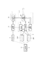
図1は第1の実施形態による光学式座標入力装置の構成を示すブロック図である。図1が示すように、装置は座標入力面であるスクリーン10に対して光スポットを形成する指示具4と、スクリーン10上の光スポット5に関する位置座標及びその他のパラメータを検出する座標検出器1とを含む。図1において、それらの構成と合わせて、出力装置として、スクリーン10に画像、或いは前述の位置情報等を表示する投射型表示装置8も記載されている。
【0018】
図2は指示具4の構成を示すブロック図である。指示具4は、光ビームを発射する半導体レーザ、或いはLED素子、電球等の発光素子41と、その発光を制御する発光制御部42、複数の操作用スイッチ43A〜43D(以下、これらのスイッチをひとまとめにいう場合、スイッチ43という)、本実施形態では電池を用いている電源部44とを含む。電源部44は、主電源或いは自家発電によっても良い(a mains connection or a manually-operated generator.)。
【0019】
発光制御部42は、所定周期の周波数で発光のON(オン)及びOFF(オフ)をするよう発光素子41を制御し、更に後述する変調方法とによって、制御信号を発光に重畳することができる。交互に起こる発光のON時とOFF時の間で、2つの明るさのレベル(HIGHとLOW)となる。この発光周期は、操作者により視認されるフリッカーと区別されるべく、十分高速なものとする。
【0020】
本実施形態においては、ON及びOFFはまたHIGH及びLOWである場合を含む。制御信号変調は操作スイッチ43Aから43Dの状態に応じて2つの状態を交互に生成する光ビームを可能とする。この制御信号変調においても、前述と同様にフリッカーと区別され得る周期とする。指示具は4つのスイッチ43Aから43Dを示しているが、他の数及び配置が可能である。
【0021】
また、図1において、座標検出器1はスクリーン10を透過した指示具4からの光を検出する。座標検出器1は座標検出センサ部2と、座標検出センサ部2の制御および座標演算などを行うコントローラ3、制御信号検出センサ(受光素子)6と、信号処理部7とを含む。
【0022】
座標検出器1は、スクリーン10上の光スポット5の位置座標及び指示具4の各スイッチの状態に対応する制御信号とを検出する。座標検出器1はその検出した情報を出力手段3Aを介してコンピュータ200のような外部装置に送る。外部装置はRAM202及びROM203といったデータやプログラム等を記憶するためのメモリを備える処理部201と、キーボード204やマウス205のような入力装置と、脱着可能なディスク207へのデータの読み取り及び書き込みをするディスクドライブ206と、表示器208とを含むコンピュータ200である。プリンタ209もまたコンピューター200に接続可能であり、モデム210を用いることにより、ネットワークにおけるデータの交信を可能とする。
【0023】
投射型表示装置8は、発光光学系と投影レンズを含む。発光光学系は、外部装置200から出力される画像信号を受けて液晶パネル82を制御する制御信号を提供する画像信号処理部81を含む。投射型表示装置8は更にランプ83、ミラー84、コンデンサーレンズ85を含む。投射型表示装置8は任意の画像をスクリーン10に表示することができる。スクリーン10は投射画像の観察範囲を広くするための適度な光拡散性を持つ。このため、指示具4により発光された光ビームもまたスクリーン10を伝わって光スポット5の位置で拡散される。光スポットのスクリーン上での位置や指示具4の光ビーム45のスクリーン10の面に対する方向によらず、座標検出器1は拡散された光の一部を検出できる。
【0024】
本実施形態の座標入力装置によれば、スクリーン10上で光スポット5を移動させることにより、スクリーン10上で文字情報や線画情報を入力することができ、操作スイッチ43Aから43Dを使って指示具4により発光する光ビームを変調することができる。光スポット5に関する座標情報及び変調情報は出力手段3Aを介してコンピュータ200に送られる。その情報を投射型表示装置8を用いて表示すべく、その情報は処理され、コンピュータ100から信号処理部81に送られる画像信号に作用する。指示具4は入出力手段としても使用される。例えば画面に表示されるカーソルの移動、スクリーンに表示されているボタンの指示、或いはアイコンを選択することによる入力操作の実行などである。以下、本実施形態の光学式座標入力装置の詳細に付いて具体的に説明する。
【0025】
<指示具4の詳細説明>
発光制御部42は発光素子41の発光のON及びOFF(或いはHIGHレベル及びLOWレベル間で交互に発光する)及び後述する変調方法とによる制御信号の光への重畳といった制御を行う。制御信号の種類は操作スイッチ43Aから43Dの状態に応じて定まる。指示具のスイッチ入力と制御信号との関係を表す真理値表を図3に示す。
【0026】
図3において、スイッチA〜Dは図2におけるスイッチ43Aから43Dに対応し、“発光”は光スポット5を作る発光素子41の光ビームの発光に対応し、“ペンダウン”及び“ペンボタン”は光ビームの変調により送られる制御信号に対応する。
【0027】
操作者は、指示具4を握ってスクリーン10に向ける。スイッチ43Aは操作者の親指に便利な位置に配置されている。スイッチ43Aが押されると光ビーム45が発光される。光スポット5はスクリーン10上に生成され、座標信号が出力され始める。この状態では、ペンダウン及びペンボタンの制御信号はOFFの状態である。このため、スクリーン上の座標位置のみが出力手段3Aから出力される。
【0028】
スイッチ43C及び43Dは操作者の人差し指及び中指に便利な位置に配置されている。これらのスイッチが押されると、図3に示されるようにペンダウン及びペンボタンに対応する制御信号が光ビームに重畳される。すなわち、スイッチ43Cが押されると“ペンダウン”制御信号が光ビームを介して送られ、文字や線画の入力、アイコンとしてスクリーンに表示されているボタンの選択及び決定などの画面制御機能を実行できる。
【0029】
スイッチ43Dが押されると“ペンボタン”制御信号が光ビームを介して送られ、メニューの呼び出しなどの別機能を実行できる。
【0030】
これにより、操作者はスクリーン10上の任意の位置ですばやく正確に文字や図形を描いたり、ボタンやメニューを選択決定したりすることができ、効果的な操作が可能となる。
【0031】
指示具4を直接入力専用として使用する、即ちポインタとして使用せず、スクリーンに接触して使用する指示具とするならば、光ビームを生成する必要はなく拡散光を指示具の光源として用いることができる。これは、半導体レーザよりも安価で長寿命のLEDを用いることを可能とするものである。
【0032】
図1に示したシステムはリアプロジェクションシステム、即ち表示装置がスクリーン10の後方(オペレーターから見てスクリーンの逆の位置)に位置する構成である。表示装置からの画像出力はスクリーンの後方から投影される。指示具4により発光される光はスクリーン10を通過した後に座標検出器1に到達する。一方、図23に示すような、表示装置から出力される画像を部屋の壁や不透明なスクリーンに投影するフロントタイププロジェクションが普及しており、本発明はこのようなシステムでも使用可能である。
【0033】
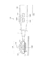
フロントプロジェクションタイプの座標検出器100(図23)の構成は、前述したリアプロジェクションタイプのシステムとほぼ同様であるので、詳細な説明は省略する。ただし、フロントプロジェクションタイプの実施形態においては、光の位置はスクリーン110を介さずに検出されなければならない。このようなフロントタイププロジェクションシステムで用いられる指示具140の構成を図23及び図24を用いて以下に説明する。
【0034】
指示具140は伸縮自在のセンター部Cを有し、その一端にはグリップ部140aを備える。グリップ部140aには操作スイッチ143A、143C及び143Dと、電源部144及び発光制御部142といった内部処理手段が備わっている。発光源141はセンター部の多端に位置する先端部146に配置される。先端部146は発光素子141、スイッチ143B,透明保護カバー147とを備える。発光素子141とカバー147とは、スイッチ143Bがスクリーン110に押圧されたときに発光素子141から発光された光がスクリーン110から遠ざかる方向に進むような関係に構成されている。
【0035】
従って、このシステムにおいては発光145の一部がスクリーン110を通過することなく座標検出器100に到達することができる。スイッチ143Bはスクリーンに押圧されることによって操作され、発光素子141は発光を開始する。発光素子141により発光された光の一部が保護カバー147を介して座標検出器100に到達するが、保護カバー147が光145が指示具140の長さ方向に向かって幅広い光拡散をするような光拡散性とレンズ機能を持つことにより、例え指示具の角度が変わっても光は座標検出器100に到達できる。図24に示した指示具140に含まれる各処理手段は、図2の指示具において対応する番号(下2桁が一致する番号)を付された各手段と同様の機能を有する。
【0036】
例えば、投影型表示装置が座標検出器及び指示具なしで会議において用いられた場合、話者は投影型表示装置からの光を遮ることを避ける為に投影型表示装置とスクリーンの間に立つことができず、スクリーン上の位置を特定するためにポインターのような道具が使用される。プレゼンテーションを進めるにあたり、話者は表示する画像の変更を指示する為に画像の表示を制御しているコンピュータの所に移動するか、或いはその操作の為にコンピューターの所に他の人を配置することが要求される。
【0037】
しかしながら、図23及び図24に示されるシステムでは、話者はコンピュータの所に移動することなく所望の位置に情報を加えたり位置情報を入力したりすることができる。更に、同様にしてスクリーンマウスのように機能させて、コマンド入力ボタンとしてのアイコンをクリックすることにより、移動したり他者の補助を求めることなく話者は自在にコンピュータを制御することができる。
【0038】
また、図2の指示具4のスイッチ43Bは指示具4の一端に設けられている。同様に図24の指示具のスイッチ143Bが指示具140の一端(グリップ140aの多端)に設けられている。スイッチ43B及びスイッチ143Bは、スクリーン10或いは110に押し付けられることによって動作する。操作者は指示具4或いは140を握り、指示具4の端或いは先端部をスクリーン10或いは110に押し付けると“ペンダウン”制御信号が指示具4或いは140から発光される光ビームに重畳される。座標検出センサ部2は光スポット5の位置を検出し、制御信号検出センサ6は光ビームに重畳されている制御信号を検出する。図3の表に示されているように、発光がONかつ指示具がスクリーンに押されているときは、位置信号と制御信号の両方が光ビームを介して転送されている。従って、自然な入力のためのペン操作に余分なボタン操作は不要となる。
【0039】
スイッチ43A及び143Aはペンボタンの一部として機能する。指示具を画面に押し付けない状態でスイッチ43Aを押せば、位置信号のみが出力され、外部装置においてスクリーンカーソルの位置制御に用いることができる。実際上、文字や図形の入力は画面から離れて行うより、直接画面に触れた方が遥に操作性、正確性が良い。本実施形態では、このように4個のスイッチを用いて画面から離れていても、また、直前にいても、自然で快適な繰作が可能であり、各状況に応じて使い分けることができるように構成されている。
【0040】
また、近接用、遠隔用の2種類の指示具4或いは140を用いたり、同時に2人以上で操作する、あるいは色や太さなど属性の異なる複数の指示具4を用いるといった場合のために、発光制御部42(142)は、ID番号等の固有の識別信号を光ビーム45或いは145の変調情報の一部として送信するように設定されている。なお、送信された装置のID番号に対応して、指示具4或いは140により描かれた線の太さや色などの属性を外部接続機器のソフトウェアなどで決定するようにも構成できる。各装置における線の属性は、スクリーン10上のボタンやメニューなどを用いて設定及び変更することができる。また、この操作は、指示具4(140)に別途操作ボタン等を設けて変更指示信号を送信するようにしてもよい。これらの設定については指示具4(140)内部あるいは座標検出器1(100)内に状態を保持するようにして、ID番号ではなく、例えば線の太さや色を示す属性情報を外部接続機器へ送信するように構成することも可能である。
【0041】
このような追加の操作ボタンは、他の機能にも使用可能である。例えば表示装置の点滅や信号源の切換、録画装置や外部装置(コンピュータ200)、或いは端子3Aとは別の予備出力端子を介して直接接続された座標検出器1の制御である。さらに、スイッチ43Aと43B(或いは143Aと143B)のいずれか一方、または両方に圧力検出手段を設けることにより、筆圧検出を行ってこの筆圧データを制御信号と共に送信することができる。このような方法により、各種の有用な信号を座標検出器1に送信することが可能である。
【0042】
指示具4のスイッチ43Aまたはスイッチ43BがONになると発光が開始され、図7のLSG信号に示すような発光信号が出力される。すなわち、本実施形態の発光信号は、比較的長い連続するパルス列からなるリーダ部(LEADER)と、これに続くコード(メーカーIDなど)とからなるヘッダ部がまず出力され、その後、ペンIDや制御信号などからなる送信データ列が予め定義された順序と形式に従って順次出力される。
【0043】
本実施形態では各データビットにおいて、“1”ビットは光を受けていない3つのクロックインターバルが続いている光を受けていることを示すクロックインターバルにより定義され、“0”ビットは光を受けていない一つのクロックが続いている光を受けていることを示すクロックインターバルにより定義されている。この変調方式では“1”ビットは“0”ビットの2倍のインターバルを必要としている。しかしながら、データの符号化方式については種々のものが使用可能である。後述する様に、効果的な座標検出のためには平均光量が一定していること、またPLLの同調を行うにはクロック成分が十分大きいことが望ましい。また、送信すべきデータ量から見て冗長度を比較的高くしても支障はないことを勘案して、本例においては、6ビット(64個)のデータを10ビット長のコードのうち、1と0が同数で、かつ、1あるいは0の連続数が3以下の108個のコードに割り付ける方法で符号化している。このような符号化方式をとることによって、平均電力が一定になり、また十分なクロック成分が含まれるので、復調時に容易に安定した同期信号を生成することができる。
【0044】
また、前述したように、ペンダウンおよびペンボタンを表す制御信号に2ビットの信号を用いるが、IDなどその他の長いデータも送信しなければならない。そこで、本例では、24ビットを1ブロックとして、先頭の2ビットは制御信号、次の2ビットは内容識別コード(例えば、筆圧信号は00、IDは11等)、次の2ビットはこれらのパリティ、その後に、16ビットのデータと2ビットのパリティとを並べて、1ブロックのデータとして構成する。このようなデータを前述したような方式により符号化すると、40ビット長の信号になる。その先頭に10ビット長のシンクコードを付加する。このシンクコードは0が4個、1が5個連続する、あるいはその反転パターン(直前のブロックの終わりが、1か0かで切り替える)という特殊なコードを使用して、データワードとの識別が容易で、データ列の途中においても確実にその位置を識別してデータの復元ができるようになっている。従って、1ブロックで50ビット長の伝送信号となり、制御信号と16ビットのIDまたは筆圧等のデータを送信していることになる。
【0045】
本例では、第1の周波数60kHzの1/8の7.5kHzを第2の周波数としているが、前述のような符号化方式を採用しているため、平均伝送ビットレートは、この2/3の5kHzとなる。さらに、1ブロックが50ビットなので、100Hzでは1ブロック24ビットのデータを送信していることになる。したがって、パリティを除いた実効ビットレートは、2000ビット/秒である。このように冗長性は高いが、誤検出を防止し、同期を容易にすることが非常に簡単な構成で通信を実現できる方式となっている。また、後述のセンサ制御のための位相同期信号と、シンクコードの繰り返し周期のチェックとを併用することによって、信号に短いドロップアウトが発生した場合でも追従ができ、逆に実際に、ペンアップやダブルタップのような素早い操作を行った場合との識別は、ヘッダ信号の有無によって確実に行えるようにもなっている。
【0046】
<座標検出器1の詳細説明>
図4は、座標検出器1の内部構成を示す。この座標検出器1には、集光光学系によって高感度に光量検出を行う受光素子6と、結像光学系によって光の到来方向を検出する2つのリニアセンサ20X,20Y(座標検出センサ部2を構成する)とが設けられている。表示装置としてリアタイプを用いるかフロントタイプを用いるかに拠らず、座標検出処理は同じである。以後、リアタイプの実施態様について説明するが、フロントタイプの場合においても光スポットの位置の検出は同様に実行される。
【0047】
座標検出装置1は指示具4に内蔵された発光素子41からの光ビームにより、スクリーン10上に生成された光スポット5からの拡散光を受光する。コントローラ3は、センサ制御部31、AD変換部31A、座標演算部32、通信制御部33を有し、コントローラ7は周波数検波部71、制御信号検出部72を備える。各部の機能は以下の説明から明らかとなろう。
【0048】
<集光光学系の動作説明>
受光素子6には、集光光学系としての集光レンズ6aが装着されており(図1)、スクリーン10上の全範囲から高感度で所定波長の光量を検知する。この検知出力は、周波数検波部71によって検波された後、制御信号検出部72において制御信号(指示具4の発光制御部42によって重畳された信号)などのデータを含むデジタル信号が復調される。
【0049】
座標検出装置1の機能構成図を図25に示す。この装置は処理を制御及び実行する中央処理装置(CPU)301と制御プログラムや各処理において生成される様様なデータを格納するメモリ302を有する。図12、16、17及び20のフローチャートに示した各種処理を実行するための制御プログラムはメモリ302に記憶され、CPU301はこの制御プログラムに基づいて処理を実行する。従って、図4に示した座標演算部32、周波数検波部71及び制御信号検出部72の処理はCPU301により実行される。プログラムは処理が開始される以前にフロッピーディスクやCDROMのようなデータ保持手段から読み出すか、或いはモデム210を介して接続された通信ネットワークの外部端末からダウンロードしてメモリ302に格納することも可能である。
【0050】
メモリ302がCPU301に接続されているときには、処理はメモリ302に格納されている制御プログラムに基づいて実効され得る。通信インタフェース303は本装置と他の装置、例えばコンピュータ200、情報処理部、形態端末、電話等(図示せず)との間の通信を制御する。通信インターフェース303は信号或いはデータの転送及び受信を制御する。信号或いはデータは本装置と外部装置との間を、公衆回線、インターネット、LAN(Local Area Network)等のネットワークを介して転送及び受信され得る。入力インタフェース304は信号及びデータの入力を制御し、出力インタフェース305は信号及びデータの出力を制御する。センサ307、センサ制御部306及びAD変換部308は図4におけるユニット2、31及び31Aに対応する。
【0051】
図25においては、装置内にセンサ307、センサ制御部306及びAD変換部308を有したが、センサ307は他の手段と切り離して他の装置に配置することも可能である。ここでは、入力インタフェース304はセンサ307から転送された信号を受信し、それらをセンサ制御部306かAD変換部308に送り、出力インタフェース305はセンサ制御部306から外部センサ307への信号及びデータの転送制御を行うものである。更に、センサ307だけでなくセンサ制御手段306或いはAD変換部308も他の外部装置に配置可能である。その場合、入力インタフェース304はセンサ制御部306或いはAD変換部308から転送されてくる信号及びデータを受信し、他の内部手段に送る。出力インタフェース305は他の内部手段からの信号及びデータをセンサ制御部306或いはAD変換部308に転送する。入力インタフェース304及び出力インタフェース305における装置と外部装置との間の通信における処理は、CPU301により制御される。図25の装置における各手段はバス309により接続され、信号及びデータがそれらの間を転送される。
【0052】
なお、図25に示されている装置は、処理や入力信号及びデータの状況を示す画像やメッセージを表示する表示器、処理を制御する為の指示を入力するためのキーボードやポインティングデバイスなどの入力手段をも備え得る。
【0053】
図7は、制御信号の復元動作を説明するタイミングチャートである。先に述べたようなビット列からなるデータ信号は、受光素子6で光出力信号LSGとして検出され、周波数検波部71で検波される。周波数検波部71は、光出力信号LSGの中で最も高い第1の周波数のパルス周期に同調するように構成され、光学的なフィルタと併用することによって、外乱光の影響を受けることなく、変調信号CMDを復調する。この検波方法は広く実用されている赤外線リモートコントローラと同様であり、信頼性の高い無線通信方式である。本例では、この第1の周波数としては、一般に使用されている赤外線リモートコントローラより高い帯域である60KHzを用い、赤外線リモートコントローラを同時に使用しても誤動作することのないように構成してある。しかしながら、この第1の周波数を一般に使用されている赤外線リモートコントローラと同じ帯域にすることも可能であり、このような場合にはIDなどで識別することによって誤動作を防止することになる。
【0054】
さて、周波数検波部71により検波された変調信号CMDは、制御信号検出部72によってデジタルデータとして解釈され、前述した“ペンダウン”や“ペンボタン”などの制御信号が複元される。この複元された制御信号は、通信制御部33に送られる。また変調信号CMDに含まれる第2の周波数であるコード変調の周期は、センサ制御部31によって検出され、この信号によってリニアセンサ20X,20Yを制御する事になる。すなわち、センサ制御部31では、図7に示したヘッダ部のタイミングで各部をリセットし、その後、変調信号CMDの立ち下がりに位相同期した信号LCKを生成する。従って、この生成された信号LCKは、指示具4の発光の有無に同期した一定周波数の信号となる。また、変調信号CMDからは、光スポットが現れた時にハイレベルを生成し、指示具が光を投影しなくなった時にローレベルを生成する信号LONと、この信号LONによって起動されるセンサリセット信号RCLとが生成される。このセンサリセット信号RCLがハイレベルの間に2つのリニアセンサ20X,20Yはリセットされ、信号LCKの立ち上がりに同期したセンサリセット信号RCLの立ち下がりのタイミングによって後述する同期積分動作が開始される。
【0055】
一方、制御信号検出部72は信号中のヘッダ部を検出し、他の機器やノイズではなく、指示具4からの入力が開始されたことを確認すると、この確認を示す信号が通信制御部33からセンサ制御部31に伝達され、リニアセンサ20X,20Yの動作有効を示す信号CONがハイレベルにセットされ、座標演算部32の動作が開始される。
【0056】
図8は、光出力信号LSGが無くなり、一連動作の終了時におけるタイミングチャートを示す。光出力信号LSGから検波された変調信号CMDがローレベルを一定時間以上続けると、光入力の有無を示す信号LONがローレベルになり、さらに、センサ動作有効を示す信号CONもローレベルとなる。そして、その結果、リニアセンサ20X,20Yによる座標の出力動作が終了する。
【0057】
<結像光学系の動作説明>
図5は、2つのリニアセンサ20X,20Yの配置を示す図である。結像光学系としての円筒レンズ90X、90Yによって光スポット5の像が各センサの感光部21X,21Yに線状に結像する(91X,91Y)。これら2つのセンサを正確に直角に配置することによって、それぞれがX座標、Y座標を反映した画素にピークを持つ出力が得られる。そして、これら2つのセンサは、センサ制御部31によって制御され、出力信号はセンサ制御部31に接続されたAD変換部31Aによってデジタル信号に変換されて座標演算部32に送られる。座標演算部32はこれらのデジタル信号から出力座標値を計算し、その結果を制御信号検出部72へ提供する。制御信号検出部72は、座標演算制御部32からの座標値を、制御信号などのデータと共に通信制御部33を介して、所定の通信方法で外部制御装置(例えばコンピューター200)に送出する。
【0058】
また、調整時など通常と異なる動作(例えば、ユーザ校正値の設定)を行わせるために、通信制御部33の方からセンサ制御部31、座標演算部32へモード切換え信号が送られる。
【0059】
本実施形態では、光スポット5の像が各センサの画素の数倍の像幅となるように焦点調節を行って、故意にボケを生じさせている。直径1.5mmのプラスチック製の円筒レンズと画素ピッチ約15μm、有効画素が64画素のリニアCCD及び赤外線LEDを用いた実験によれば、最もシャープな結像をさせると、約40度の画角全面にわたって15μm以下の像幅となり、このような状態では画素間分割演算結果が階段状に歪んでしまうことがわかった。これに対して、像幅が30μmから60μmとなるようにレンズの位置を調節すると、非常に滑らかな座標データが得られる。もちろん、大きくボケさせると、ピークレベルが小さくなってしまうので、数画素程度の像幅にするのが最適であると思われる。画素数の少ないCCDと、適度な画素数の像幅を持つ線像を形成する光学系を用いることが、本実施形態のポイントの一つであり、このような組み合わせを用いることによって、演算データ量が少なく、小さなセンサと光学糸で非常に高分解能、高精度、高速でかつ低コストな座標入力装置を実現できる。
【0060】
アレイ状に配置されたX座標検出用リニアセンサ20X,Y座標検出用リニアセンサ20Yは同一の構成であるので、以下ではX座標検出用リニアセンサ20の構成について説明する。図6はX座標検出用リニアセンサ20X(Y座標検出用リニアセンサ20Y)の内部構成を示すブロック図である。
【0061】
受光部であるセンサアレイ21はN個の画素(本実施形態では64画素)からなり、受光量に応じた電荷が積分部22に貯えられる。積分部22は、N個からなり、ゲートICGに電圧を加えることによってリセットできるため、電子シャッタ動作が可能である。この積分部22に貯えられた電荷は、電極STにパルス電圧を加えることによって蓄積部23に転送される。この蓄積部23は、2×N個からなり、指示具4の発光タイミングに同期した信号LCKのH(ハイレベル)とL(ローレベル)とのそれぞれに対応して別々に電荷が蓄積される。この結果、発光素子の点灯時と非点灯時で別々に電荷が蓄積される。その後、光の点滅に同期して各々別々に蓄積された電荷は、2×N個からなるシフト部24を介して、2×N個からなるリニアCCD部25に転送される。このシフト部24は転送クロックを簡単にすべく設けられている。
【0062】
これにより、リニアCCD部25には、N画素の各画素毎に、点灯時と非点灯時のセンサ出力に対応した、計64画素の電荷が隣接して並んで記憶されることになる。これらリニアCCD部25に並べられた電荷は、2×N個からなるリングCCD部26に順次転送される。このリングCCD26は、信号RCLに応じてCLR部27で空にされた後、リニアCCD部25からの電荷を順次蓄積していく。
【0063】
このようにして蓄積された電荷は、アンプ29によって読み出される。このアンプ29は、非破壊で蓄積電荷量に比例した電圧を出力するものであり、実際には、隣接して格納されている電荷量の差分、すなわち、N画素の各画素について、その画素の発光素子41の点灯時の電荷量とその画素の発光素子41の非点灯時の電荷量との差分に対応する値を増幅して出力する。
【0064】
また、センサを、エリアセンサとして構成する場合は、分解能を2倍にするには、4倍の画素数と演算データとが必要となるのに対して、リニアセンサとして構成する場合には、X座標,Y座標各々2倍の画素数にするだけで済む。従って、画素数を増やしてさらに高分解能にすることも容易にできる。
【0065】
また、線上に光電変換素子を配列したセンサ(20X及び20Y)を用いる例を説明したが、光電変換素子を2次元に配列したセンサを用いることもできる。この場合、円筒形レンズ(90X及び90Y)の替わりにボケた点像が得られるような構成の集光レンズを用いる。光電変換素子の出力を各光電変換素子の二次元位置情報に関連付けてメモリに格納し、その格納された光電変換素子の出力信号から差分信号が最大となるpeak画素を求め、そのpeak画素を中心とする円状、或いは円内の画素の差分信号から閾値を求めるという処理を実行する。この場合、分解能を2倍にするには、4倍の画素数と演算データとが必要となるのに対して、リニアセンサとして構成する場合には、X座標,Y座標各々2倍の画素数にするだけで済む。従って、画素数を増やしてさらに高分解能にすることも容易にできる。
【0066】
図9は、リニアセンサ20X,20Yの出力波形の一例を示す図である。図中、縦軸は電荷量を、横軸は画素位置を示す。Bの波形は発光素子41の点灯時に読み出した信号の波形であり、Aの波形は非点灯時の波形であって、即ち外乱光のみの波形を示すものである(図6を用いて説明したように、リングCCD26には、これらA,Bの波形に対応する画素の電荷が隣接して並んでいる)。アンプ29は、その隣接する電荷量の差分値(B−Aの波形)を非破壊増幅して出力するが、これにより指示具4からの光のみの像の信号を得ることができ、外乱光の影響を受けることなく安定した座標入力が可能となる。
【0067】
ここで、図9に示したB−Aの波形の最大値をPEAK値と定義する。光に対してセンサが機能する蓄積時間を増大させる、即ち、連続するクロックの間電荷を蓄積し続けた場合、その時間に応じてPEAK値は増大する。言い換えれば、信号LCKの1周期分の時間を単位蓄積時間とし、それを単位として蓄積回数nを定義すれば、蓄積回数nを増大させることでPEAK値は増大する。このPEAK値が所定の大ささTH1に達するまで検出を続けることで、常に一定した品位の出力波形を得ることができる。
【0068】
外乱光が非常に強い場合、差分波形B−Aのピークが十分な大ささになる前に、リングCCD26の転送電荷が飽和してしまう恐れがある。このような場合を考慮して、センサにはスキム機能を有するスキム部28が付設されている。スキム部28は、非点灯信号のレベルを監視し、図10に示されるように、n回目のクロック周期であるAnにおいて信号レベルが所定の値(図中、一点鎖線のレベル)を超えている場合、一定量の電荷を各画素の蓄積電荷から抜き取るようにする。これにより、次のn+1回目には、波形An+1が得られる。信号が閾値より下になるまで電荷の抜き取りを繰り返すことによって、非常に強い外乱光があっても飽和しない。従って、点滅光の光量が微弱であっても、複数回積分動作を継続することによって、十分な大ささの信号波形を得ることが可能になる。特に指示具4に可視光域の発光源を用いる場合、表示画像の信号が重畳するので、前述したスキム機能と差分出力を用いることによって、非常にノイズの少ないシャープな波形を得ることが可能となる。
【0069】
また非常に強い外乱光が入射された場合には、前述のPEAK値を監視し、そのPEAK値が所定レベルに達した時に前述の蓄積動作を停止させても良い。つまりこのような場合には、蓄積処理を増大させなくても十分な品位の出力波形が得られるので、信頼性の高い座標演算が可能となるとともに、蓄積回数が比較的少なくて済むことから、入射光が弱い場合に比べて、単位時間あたりの座標算出サンプリングレートが向上する(たとえば20点/秒で座標算出としていたものが40点/秒とより高速で座標演算が可能という意味)という利点が得られる。
【0070】
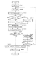
図11は、リニアセンサ20X,20Yのセンサ制御の一連の動作を示すものである。センサ制御部31は、まず、ステップS101によりセンサ制御動作を開始し、ステップS102において信号CONを監視する。そして、信号CONがハイレベルになると、ステップS103でカウンターponを1にセットし、蓄積回数nを0にリセットし、ステップS104でセンサ出力のPEAK値(ピ―クレベル)が所定の大きさTH1より大きいか否かを判定する。
【0071】
PEAK値がTH1より小さい場合はステップS105に進み、蓄積回数nが第1の所定回数n0を超えているかを判定する。超えていなければステップS106に移り、蓄積回数nを1インクリメントしてステップS104に戻る。こうして、PEAK値がTH1より大きくなるか、蓄積回数nが限界値n0を超えると、ステップS107に進み、積分停止信号RONがハイレベル(Hi)になって積分動作は停止される。そして、座標演算部32による座標値演算の処理が開始される。なお、座標演算処理については後述する。
【0072】
その後、ステップS108とステップS109のループでカウンターnが第2の所定回数n1を超えると、積分停止信号RONがローレベルになり、同時に、信号LCKの周期の数倍(図8では2倍)の間センサリセット信号RCLがハイレベルになる。その後、処理は、ステップS112に進み、信号CONがハイレベルである間はこの動作が繰り返され、上述の所定回数n1で決まる周期ごとに座標値演算が行われる。
【0073】
また、ごみなどの影響で、信号CONがドロップしても、1回のみは状態を保持するように、ステップS111が設けられている。もし、連続して2周期の間、信号CONがローレベルであれば、ステップS102からステップS113に進み、カウンターponが0にリセットされ、シンク信号待ちの状態になってステップS101に戻る。
【0074】
なお、このドロップアウト対策部分は、1周期でなくもっと長くすることも可能であるし、外乱が少なければ、無くしてしまってもよい。なお、ここの1周期を前述のデータブロックの周期の自然数倍として、シンクコードのタイミングと一致させ、信号CONの代りにシンクコード検出信号を用いても同様の動作を行える。
【0075】
座標検出器1に入射する指示具4の光は、指示具4における電源の消耗(電池の電圧変化)に応じて変化する。特に、スクリーン10の光るの拡散性が低い場合、及び表示される画像の表面輝度が増加している場合、センサに入射する光量は光スポットの位置と指示具4とに応じて様々に変化する。しかしながら本実施形態においては、このような場合であっても、このような影響を補償するべく積分回数を自動的に変化させるので、常に安定した出力信号が得られ、現実的な座標検出が可能となる。レーザーポインターのビームが直接センサに入射した場合においても、安定した座標検出が可能である。
【0076】
また、画面に直接接触させて使用するLEDを用いたペンタイプとレーザポインタとを併用する場合、LEDはより大きな光量のものが使用可能であるので、使用中の指示具がペンかポインタかに応じて図11に示した積分回数n0及びn1を切換える。ここでは、指示具がペンかポインタかの識別は、使用中の指示具から供給されるID信号に基づいて行われる。ペンが使用されている時はサンプリングを高速に、ポインタが使用されている時は低速にすることも可能である。実際、文字入力のように繊細な描画作業はポインタでは不可能であり、むしろ低速サンプリングによって滑らかな線を描けるほうが使い勝手がよい。
【0077】
以上述べてきたように、点滅光に高周波数のキャリアを加え、そのキャリアを周波数検波して得た所定周期の復調信号によって積分動作のタイミング制御を行うようにしたので、指示具と撮像部とをコードレスで同期させることができ、使い勝手の良い座標入力装置を実現することができる。
【0078】
また、レーザービームを用いることによって画面から離れた位置で容易に操作することが可能となる。また、積分手段からの差分信号中のピークレベルが所定レベルを超えことを検出し積分動作を停止させる積分制御手段を設けたので、光量が変化してもほぼ一定レベルの光スポット像の信号を作成でき、これにより、常に安定した高分解能な座標演算結果を得ることができる。
【0079】
以上、センサに入射する光量の多少にかかわらず、信号の品位を一定に保つ方法を説明したが、ここでひとつ課題が発生する。前述の光量は、先に説明したように、指示具4に内蔵された電源(電池)44の消耗により変動する他、指示具4のスクリーンに対する姿勢、つまり座標入力を行う通常の筆記動作により指示具4が傾く、あるいは、センサあるいは発行素子の変換効率の個体間差等によって、変動することが想定される。検出部に到達する光が減少した場合、その到達した光のレベルに応じて積分時間を長くする、すなわち、n0、n1の値を大きくし、積分回数を増大させることで品位の良い信号波形を得ることができるが、積分時間の増大は、座標サンプリングレート、つまり単位時間に算出できる座標点数の減少を意味し、本願発明とするところの座標入力装置として、操作者の筆跡を忠実に再現するためには、おのずと限界がある。例えば、その筆跡を忠実に再現するために25点/秒の座標算出サンプリングレートが必要であると仮定すれば、1回の座標算出動作時間は少なくとも40mSEC以下であることが必要であり、その時間内の積分時間で信号波形が所定のピークレベルに到達することが求められる。しかしながら、所定レベルのピークレベルが得られなかった場合でも、信頼性の高い座標を算出することが可能となれば、操作者にとって筆記性の良い指示具(例えば指示具の傾きより大きくできる)を実現可能であり、また電池寿命を延ばすことも可能となる。
【0080】
<座標値演算>
以下、座標演算部32における座標演算処理について説明する。
【0081】
上述のようにして得られた2つのリニアセンサ20X,20Yの出力信号(アンプ29からの差分信号)は、センサ制御部31に設けられたAD変換部31Aでデジタル信号として座標演算部32に送られ、座標値が計算される。座標値の演算では、まず、X座標、Y座標の各方向の出力データに対して、センサ上の座標値(X1,Y1)が求められる。なお、演算処理は、X座標もY座標も同様であるので、以下ではX座標に関する演算を説明する。
【0082】
図12は第1の実施形態による座標計算の手順を説明するフローチャートである。座標計算処理が開始されると、まずステップS201で変数contが0にセットされる。変数contは基準点設定モード(後述)において用いられる。そして、ステップS202において、任意の座標入力点(後述する基準点設定モードでは座標が既知の所定点)での各画素の点灯時と非点灯時の出力値の差分信号である差分データDx(n)(本実施形態の場合画素数n=64)が読み込まれ、バッファメモリに貯えられる。次に、ステップS203では、あらかじめ設定しておいた閾値VとDx(n)とを比較し、閾値以上のデータ値Ex(n)を導出する。このデータEx(n)を用いて、ステップS204でセンサ上の座標X1を算出する。本実施形態では重心法により出力デ―タの重心を算出しているが、出力データEx(n)のピーク値を求める方法(例えば微分法による)等、計算の方法は複数あることは言うまでもない。
【0083】
ステップS205で座標演算処理のモード判定を行う。出力データの重心X1から座標を算出するためには、あらかじめ所定値を求めておく必要があり、その所定値を導出する方法(基準点設定モード)について述べる。
【0084】
同様にX方向のみについて説明すれば、スクリーン10上のX座標、Y座標が既知の2点(α0,β0)、及び(α1,β1)に指示具4からの光スポットを順次位置せしめ、前述のステップS202〜S204を各々実行し、各々の点で得られるX方向センサの重心値を、X10,X11として導出し、その値、及び既知の座標値α0,α1を各々ステップS210で記憶する(2回の繰り返しにより、X1cont及びαcontとして、X10,X11及びα0,α1が得られる)。
【0085】
そして、通常の座標算出時には、ステップS210で格納された値(X10,X11及びα0,α1)を用いて、ステップS206で座標入力点のX座標を算出する。ステップS207ではより高性能な座標入力装置を提供することを目的として、必要に応じて座標値の校正(例えば光学系のレンズ収差を補正するためにソフト的な演算でその歪みを補正する等)を行い、座標値を確定する。
【0086】
以上の処理において、確定した座標をそのままリアルタイムで出力することも可能であるし、目的に応じてデータを間引く(例えば確定座標10個毎で1個のデータのみ出力)等も可能である事は言うまでもないが、以下の仕様等を想定する場合には、これらの処理の選定は重要である。
【0087】
指示具4をペンのように使う場合と、ポインタとして画面から離れて使う場合では、使用者の手の安定性が異なる。ポインタとして使う場合には、画面上のカ―ソルが細かく震えてしまうので、このような細かい動きを抑制したほうが使いやすい。一方、ペンのように使う場合には、できるだけ忠実に速く追従することが求められる。特に文字を書く場合などには小さな素早い操作ができないと、正しく入力できなくなってしまう。
【0088】
本例では、制御信号によりIDを送信しているため、その装置がポインタとして使われているかペンとして使われているか、端のスイッチが押されているか否かの検出により判定することができる。装置がポインタとして使われている時は、既に求められている出力座標値(X−1,Y−1)、(X−2,Y−2)から推測することにより現在の出力座標値(X,Y)を求めることができる。実際、有用な構成においても少しの補正はある。本例では、単純な移動平均を用いているが、このような平滑化処理に用いる関数としては、他にも差分絶対値を大きさにより非線型圧縮したり、移動平均による予測値を用いてこれとの差分を非線型圧縮するなどの各種方式が使用可能である。要は、ポインタとして使用している場合は平滑化を強目にし、そうでない場合は弱めに切り替えることが、制御信号により可能であるため、それぞれ使い勝手のよい状態を実現可能であり、この点でも本実施形態の効果は大きい。
【0089】
なお、これらの演算処理は、前述したように座標サンプリング周波数が100Hzの場合には10msecの間に終了すればよく、原データは64画素×2(各々xおよびy座標に対応する)×AD変換部8ビットと非常に少ない上、収束演算も必要ないので低速の8ビット1チップマイクロプロセッサで十分処理が可能である。このようなことは、コスト的に有利なだけでなく、仕様変更が容易で、開発期間の短縮や様々な派生商品の開発が容易になる利点もある。特に、エリアセンサを用いる場合のように、高速の画像データ処理を行う専用のLSIの開発などは不要であるので、開発費用、開発期間などの優位性は非常に大きなものである。
【0090】
上述したような演算処理によって求めた座標値(X,Y)を示すデータ信号は、座標演算部32から通信制御部33に送られる。この通信制御部33には、そのデータ信号と、制御信号検出部72からの制御信号とが入力される。そして、これらデータ信号および制御信号は、ともに所定の形式の通信信号に変換され、外部の表示制御装置に送出される。これにより、スクリーン10上のカーソルやメニュー、文字や線画の入力などの各種操作を行うことができる。前述したように、64画素のセンサを使った場合でも、1000超の分解能と十分な精度とが得られ、センサ、光学系ともに小型、低コストな構成でよく、また、演算回路も非常に小規模な構成とすることが可能な座標入力装置を得ることができる。
【0091】
また、センサを、エリアセンサとして構成する場合は、分解能を2倍にするには、4倍の画素数と演算データとが必要となるのに対して、リニアセンサとして構成する場合には、X座標,Y座標各々2倍の画素数にするだけで済む。従って、画素数を増やしてさらに高分解能にすることも容易にできる。
【0092】
以上説明したように、本実施形態によれば、指示具4により所定の周期で点滅する光スポットの点灯時と非点灯時との信号を別々に積分して差信号を求め、ピ―ク画素の位置を精度よく求める様に構成したので、高精度、高分解能の座標値を得ることができ、さらには外乱光の影響を抑制し、小型、軽量、低コストな装置を実現することができる優れた効果が得られる。
【0093】
[第2の実施形態]
上記第1の実施形態では、図12で示した座表計算処理において電圧Vに対応する固定された閾値TH1と差分データDx(n)との比較を行っている。このため、例えば図11の処理においてn0回の積分を行ってもDx(n)のPEAK値がTH1を越えない場合、すなわち光量が不足している場合には座標検出精度が低下することになる。一方、十分な光量を得るためにn0を増加させれば検出速度の低下を招くことになる。第2の実施形態はこのような状況に対処するものである。
【0094】
<光量と座標算出サンプリングレート>
第1の実施形態で述べてきたように、指示具4に内蔵された発光素子41からの光を、センサ20の積分動作により安定した信号として検出する事ができる。しかしながら、発光素子からセンサ20へ到達する光量が減少すると、検出信号のピークレベルを所定レベルに到達させるために積分動作がより多くの回数繰り返されなければならず、ひいては座標算出サンプリングレート(単位時間で座標算出可能な点数)が低下する。座標入力装置としてユーザによる筆記を忠実に再現するためには、数十点/sec程度のサンプリングレートが望まれ、好ましくは100点/sec程度の実力が求められる。一方、本実施形態の構成で発光素子41にLEDを用いた場合、実使用状態を想定、或いは量産を考慮(個体間差を考慮)して実験を行った結果、最悪ではLEDから発せられる光量の数%程度しかセンサ20に到達することができない。一方、光量を増大させる一方法としては、LEDの順方向電流をより大きくしてLED発光量を増す事が挙げられるが、これは指示具4に内蔵された電源部(電池)44の消耗を増大させ、電池寿命を減少させる。電源部44を充電可能とする打開策も考えられるが、充電回数の増加をもたらす等、ユーザにとって実使用上好ましい状態とは言えず、発光素子41の光量をアップさせると言う観点での対策は自ずと限界が有る。この点を鑑みて成されたのが本実施形態の主眼とする所であり、その詳細に付いて以下説明する。
【0095】
本実施形態では、所定の積分動作(例えば、座標サンプリングレート100点/secを達成するために、1サンプルあたりの最大積分時間を10m/secとなるように積分回数n0,n1を設定する)を完了した際、センサから出力される信号のPEAK値がTH1に達しない場合でも、精度良く座標算出を行える様に構成したものである。図13はセンサの各画素の出力レベルを模式的に示したものであり、一般には、閾値レベルVをもって有効なデータが判別される。出力信号が十分に得られる状態では、閾値レベルVをノイズレベルから十分マージンをとって設定し、ノイズの影響を受けることなく安定した座標算出が可能である。しかしながら前述の光量不足による検出信号レベルの低下が、実使用状態の条件により想定されるので、この閾値レベルは十分小さく設定するのがより好ましい。例えば、閾値レベルをVLOWに設定すれば、より出力信号の小さなレベルでの座標算出が可能となるが、ノイズの影響を受けやすく、その算出精度は低下する。
【0096】
図16は本実施形態における座標計算の手順を説明するフローチャートである。図16に示される手順では、閾値レベルの低下に伴うノイズの影響を排除して座標計算を行う。
【0097】
処理が開始されると、まず、ステップS301で変数contが0に初期化される。そして、ステップS302では、任意の座標入力点での各画素の差分信号である差分データDx(n)(本実施形態の場合画素数n=64)が読み込まれ、ステップS311でそのDx(n)は閾値と比較されバッファメモリに各画素毎のEx(n)が貯えられる。以上のステップS301、S302、S311の処理は図12を用いて説明したステップS201〜S203の処理と同じである。
【0098】
次に、ステップS303で、出力信号が最大となる画素npeakを検出する。そして、ステップS304で最大出力信号に対応する画素npeakとその画素の両隣m画素ずつのデータを用いて(従って、用いられる画素データ数は2m+1となる)、センサ上の座標X1を以下の式に従って算出する。座標演算はこの式により行われる。
【0099】
【数1】

その他のステップ(ステップS305〜S310)については図12で述べた動作(ステップS205〜S210)と同一であり、ここでは説明を省略する。
【0101】
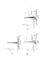
以上のステップS304に示す如く重心計算を行うことの作用効果に付いて図15を用いて説明する。図15は従来例(最も左)の計算方法、即ちすべての画素差分信号を用いて重心を求める方法と、第二の実施形態の方法、即ち重心計算に異なる画素数m(例えば各方向から選択する画素数を変える)を用いる方法との精度を示すものである。実際の光スポットの位置と検出された座標とを比較し、その差、即ち座標演算精度をスクリーン全体で10000点について求めている。計算方法と条件は横軸に示し、演算した座標の精度は縦軸に示している。図15において、“Max”はその10000点で演算された差の最大値を表し、“精度”は10000点の平均値Avg、及び標準偏差σから導出されるAvg+3σの値である。
【0102】
例えば閾値電圧を0.75Vに設定して図12に示した手順により座標計算を行うと、精度の最大値Maxが大きく劣化するばかりか、光量が不足して座標算出すら行えない領域が存在することが判明した。もちろん閾値レベルをより高くすることで、座標算出精度は向上するが、座標算出不能領域が拡大する。しかしながら図16に示した計算方法を用いてmの値を4程度に設定すれば、全領域で座標算出が可能であり、しかもその座標算出精度は実使用上十分な値が得られる。
【0103】
このことは、図12による座標計算手順に比ベ、センサで出力される信号レベルが小さくても、十分な性能を発揮できることを意味し、信頼性の高い座標入力装置を提供できるものである。また、図12による計算手順に比べ、積分時間の縮小により座標サンプリングレートを増す事も可能であり、または、LEDの発光をより弱くする事で、指示具4内に内蔵された電池44の寿命を延ばし、取り扱いのしやすい構成を実現することも可能となる。
【0104】
[第3の実施形態]
第3の実施形態では、以下のような構成を具備することによって、低光量であってもより高精度、高分解に座標を算出する事を可能とする。
【0105】
図17は第3の実施形態による座標計算の手順を説明するフローチャートである。図17に於いて、処理が開始されると、まずステップS401で変数contが0に初期化される。そして、ステップS402で任意の座標入力点での各画素の差分信号である差分データDx(n)が読み込まれ、バッファメモリにその情報を貯える。次に、ステップS403で、出力信号が最大となる画素npeakを検出する。そして、ステップS411で最大画素npeakの前後m番目の画素を選択し、両者の画素の信号レベルDx(npeak−m)及びDx(npeak+m)の比較を行う。その比較の結果、より小さい方の信号レベルを閾値に設定し、ステップS413もしくはステップS414でnpeakの両側の画素の出力信号と閾値との比較を行なう。本実施形態の場合、信号レベルがより小さい値を閾値レベルとしており、m=3とした場合のその様子を図14の(A)に示す。この図において、閾値がDx(npeak−m)に設定されている事が理解される。
【0106】
次に、ステップS415において、重心計算に用いる有効画素の判定を行う。先の動作で得られた画素nにおけるデータEx(n)が正の値であれば閾値レベル以上の信号が画素nで出力されていることが判明するが、設定される閾値レベルはPEAK値の両側の画素の出力信号に応じて変動する変動閾値であるから、光量が弱い状況ではその設定レベルがノイズレベルとなることもあり得る。最大画素npeakから十分離れた画素でノイズによる信号が出力されると、信号成分がたとえ小さい値であっても、モーメント(nEx(n)の項)として計算されるので、その誤差は少なからずとも影響する。従って本実施形態では、ステップS415で画素nにおけるEx(n)が正の値であって、最大画素npeakを含む連続した画素番号の一連の画素からの出力データのみを有効画素として判定し、演算に用いる画素の最小画素番号nmin及び最大画素番号nmaxを決定する(nmin<npeak<nmax)。その際選択される有効データを模式的に図14の(B)に示す。図16の処理ではそれらが固定であったが、図14(B)においては閾値が可変であり、演算に用いる画素の数が可変である。
【0107】
次に、ステップS404において、ステップS415で求めた有効画素、すなわち、nminからnmaxの画素を用いて、以下の式により重心X1を求める計算を行う。
【0108】
【数2】
なお、以下の処理(ステップS405〜S410)は先に説明した処理(ステップS205〜S210)と同様であり、ここでは説明を省略する。以下、上記の重心計算を用いた場合の利点に付いて説明する。
【0110】
座標入力可能有効エリアサイズが1200×900mmの座標入力装置の一部分(40×40mm)における座標算出精度を導出した様子を図18及び図19に示す。図のX軸、Y軸は入力ペン4の指示位置を示し、図のZ軸は本座標入力装置が出力したY座標値と実際の入力位置に対応するY座標値との差を示したものである。従って、その差がほぼ0と言うことは座標入力装置の精度が非常に優れている事を示す。
【0111】
図18は、上述の図16のフローチャートに示される手順で座標計算を行った結果である。同様に、図19は図17に示されるフローチャートで座標計算を行った結果である。図16で示される演算方法の測定誤差が約10mm程度であるのに対し、図17で示される演算方法で演算した結果は、その誤差が約2〜2.5mm程度と激減しているばかりか、図18に示されるような階段状の誤差の増加が発生しておらず、滑らかな誤差発生分布となっている。この事は、図16の演算方法に比べて、図17に示した演算方法は座標入力装置の分解能を更に改善していることを意味し、高精度かつ高分解能な座標入力装置を実現できる優れた効果が得られていることがわかる。
【0112】
なお、上述した実施形態では、ステップS415で有効画素を抽出するのに用いる閾値として、差分データの最大値を有する画素npeakの前後m番目の画素の差分デ―タのうちの小さいほうの値を採用した。しかしながら、この閾値の設定はこれに限られるものではなく、例えば、mの値をより大きくし、信号レベルDx(npeak−m)及びDx(npeak+m)のうち大きい値を閾値レベルとして採用しても同等の効果が得られる。或いは、例えば差分データの最大値を有する画素の前後m個の画素に対応する2m+1個の差分データから平均を求める等の所定の演算を行い、その平均或いは複合して閾値を設定しても良い。
【0113】
以上説明したように、上記実施形態によれば、指示具4により所定の周期で点滅する光スポットの点灯時と非点灯時との信号を別々に積分して差信号を求め、差分信号の最大値を有する画素(画素番号n)を検知し、この最大画素の前後m番目の画素のデータ、或いは、各々m個の画素を選択して得られる2m+1個の画素のデータを用いてデータの有効性を設定するための閾値を設定する。そして、この設定された閾値を用いて有効画素を選択し、選択された画素の出力データを用いて座標演算を行う。この結果、高精度、かつ高分解能な座標入力装置を実現することができる優れた効果が得られる。
【0114】
更に本願発明では、座標検出の信頼性を向上させるために、設定された前述の閾値が有効であるか(光信号による出力かどうか)を判定するための手段を有する。以下に説明を加えるが、その場合、次の点を十分に考慮しなければならない。これらのセンサを用いた製品を量産する場合、部品の個体間差、特に問題となるのは、センサが光をまったく受光していない時の出力電圧、つまり暗時出力電圧である。一般的な仕様として、この暗時出力電圧は±数10%変動するのが一般的であり、例えば電源電圧5Vと仮定して標準的な仕様が暗時出力電圧1Vとすれば、部品の個体間差により、その分布は0.7V〜1.3V程度となる。従って、前述した閾値レベルは1.3V以上であることが必要条件となるが、この場合暗時出力電圧0.7Vの部品で閾値電圧1.3Vという状態が存在することになる。つまり光量が弱くなってピークレベルが1.3V程度しか得られない場合には、座標演算不能になる。逆に暗時出力レベル1.3Vの部品では、閾値が1.3Vに設定されているのでノイズに対するマージンが全く設定されていないので、座標演算の信頼性が低く、より高い値に閾値を設定することが必要となる。つまり、その様な部品交差を考慮すれば、部品に応じた閾値レベルを設定することが必要であり、製品毎に調整することはコストアップの要因となることは明らかである。
【0115】
その影響を除去するために、図20において、ステップS501で処理を開始し、ステップS502では、任意の座標入力点の各画素における差分信号である差分データDx(n)(本実施形態の場合画素数n=64)が読み込まれる。この時、全画素(64画素)からの出力値の平均値を演算し、その平均値に所定のオフセット量Voffを加えて第一の閾値Vth1と定義する(ステップ503)。第1の閾値は、出力信号の有効性を判定する為に用いる(図21(A)参照)。つまり、Vth1はセンサに入力される光量、つまり信号レベルに応じて可変するとともに、前述の光量が全く入射されていない状態での暗時出力電圧にも依存することになるので、センサ個体間の部品公差を吸収し、最適な閾値レベルを自動的に設定できる。
【0116】
次にステップS504で差分データDx(n)の最大値を有する画素npeakを検出し、ステップS505でピーク画素番号npeakの前後m番目の画素の出力値、Dx(npeak―m)及びDx(npeak+m)を各々求めその値を比較する。次にステップS506、S507で比較結果に応じて第2の閾値Vth2を設定する。本実施形態の場合、Dx(npeak―m)及びDx(npeak+m)のうち、信号レベルがより小さい値を閾値レベルとしているが、m=3とした場合のその様子を図21(B)に示す。閾値がDx(npeak−m)に設定されている事が理解される。本実施形態の場合、信号レベルがより小さい値を閾値レベルとして採用しているが、mの値をより大きくし、信号レベルの高い値を閾値レベルとして採用すべく、信号レベルがより大きい方の値を閾値レベルとして設定しても良い。
【0117】
次にステップS508で第1の閾値レベルVth1と第2の閾値レベルVth2を比較する。第2の閾値レベルVth2が第1の閾値レベルVth1より大きければ、座標を計算するために十分な光がセンサに入射されたものとして、座標演算を実行する。一方、Vth2がVth1より小さい場合は、座標値を判定するために必要な光量がないとして、処理を中止し、ステップS501に戻る。
【0118】
ステップS509では、第2の閾値Vth2と各画素の出力Dx(n)が比較されバッファメモリにEx(n)が貯えられる。次に、ステップS510で、ピーク画素番号npeakを含み、閾値Vth2を越えた連続画素のみを選択し、センサ上の座標X1を算出する。なおその他のステップで行われる処理は先に述べた動作において説明した各処理と同一であるので、ここでは説明を省略する。
【0119】
本実施形態におけるステップS510において判定される有効画素を図21(C)に示す。第2の閾値Vth2はDx(npeak−m)(画素npeak−mの値)に設定されるので、この図の例においては、画素npeak−mのみならず画素npeak+mの出力値が有効画素として座標計算に用いられる。第1及び第2の閾値は可変であり、座標計算に用いられる画素数も可変であるが、図16の処理において、それらは固定値である。
【0120】
図22は座標入力可能有効エリアサイズが1200×900mmの座標入力装置におけるその一部分(40×40mm)の座標算出精度を示す。この図において誤差発生分布は滑らかであり、図20の演算が座標入力装置において好判定を得ていることが示されている。従って、その演算により、高精度及び高解像度の座標入力装置を得ることができる。
【0121】
なお、本発明に係る座標入力方法及び装置は、複数の機器(例えばホストコンピュータ、インタフェイス機器、リーダ、プリンタなど)から構成されるシステムに適用しても、一つの機器からなる装置(例えば、複写機、ファクシミリ装置など)に適用してもよい。
【0122】
【発明の効果】
以上説明したように、本発明によれば、外乱光の影響を抑制し、高分解能で高性能な座標入力装置を提供することができる。また、本発明によれば、小型で、低コストな座標入力装置を提供できる。
【図面の簡単な説明】
【図1】本実施形態に係る光学式座標入力装置の構成を示すブロック図である。
【図2】指示具4の構成を示すブロック図である。
【図3】図2の装置におけるスイッチ入力と制御出力との関連を示す表である。
【図4】図1の座標検出器の概略構成を示すブロック図である。
【図5】リニアセンサ20X,20Yの構成を示す図である。
【図6】X或いはY座標検出用リニアセンサの内部構成を示すブロック図である。
【図7】制御信号の復元動作を示すタイミングチャートである。
【図8】受光素子の出力信号から制御信号を復元する一連の動作の終了時のタイミングチャートである。
【図9】X或いはY座標検出用リニアセンサの出力波形の一例を示す図である。
【図10】リニアセンサにおけるスキム動作を示す波形図である。
【図11】リニアセンサを制御する一連の動作を示すフローチャートである。
【図12】第1の実施形態による座標演算処理を示すフローチャートである。
【図13】リニアCCDセンサの素子の出力の一例を示す図である。
【図14】リニアCCDセンサの素子の出力の一例を示す図であって、(A)は閾値の設定を示し、(B)は有効画素の抽出を示す図である。
【図15】各計算法における座標算出精度を示す図である。
【図16】第2の実施形態による座標演算処理を示すフローチャートである。
【図17】第3の実施形態による座標計算処理を示すフローチャートである。
【図18】第2の実施形態の演算処理による座標算出精度とXY位置との関係を示す図である。
【図19】第3の実施形態の演算処理による座標算出精度とXY位置との関係を示す図である。
【図20】第4の実施形態による座標計算処理を示すフローチャートである。
【図21】有効画素選択モードの例を示す図である。
【図22】第4の実施形態の演算処理による座標算出精度とXY位置との関係を示す図である。
【図23】フロント投影タイプの表示装置の構成を示す図である。
【図24】図23のフロント投影タイプの表示装置において用いる指示具を示す図である。
【図25】座標入力装置の機能構成を示す図である。[0001]
BACKGROUND OF THE INVENTION
The present invention relates to a method and an apparatus particularly suitable for a large display system capable of inputting position information such as coordinates. More particularly, the present invention relates to an apparatus and method for inputting position information such as coordinate information representing a position designated by an operator on a display screen. The operator can instruct the position using the pointing tool. The input position information can be used for processing such as controlling an externally connected computer or writing characters or figures.
[0002]
[Prior art]
As a conventional coordinate input device, a device that captures a light spot on a screen using a CCD area sensor or a linear sensor, performs image processing such as using barycentric coordinates or pattern matching, and calculates and outputs coordinate values. there were. Some coordinate input devices use a position detection element called PSD (Position Sensitive Device) (an analog device that obtains an output voltage corresponding to the spot position).
[0003]
For example, Japanese Examined Patent Publication No. 7-76902 discloses an apparatus that captures a light spot by a parallel beam of visible light with a video camera to detect coordinates, and simultaneously transmits and receives a control signal with infrared diffused light. Japanese Patent Application Laid-Open No. 6-274266 discloses an apparatus for performing coordinate detection using a linear CCD sensor and a special optical mask. On the other hand, Japanese Patent No. 2503182 discloses a configuration and output coordinate correction method for an apparatus using PSD.
[0004]
[Problems to be solved by the invention]
In recent years, the brightness of the screen of a large screen display has been improved, and it has become possible to use it even in a brightly lit environment, and its demand is expanding. In such an environment, the coordinate input device is desired to be resistant to ambient light so that it can be used in combination with such a large screen display. In recent years, devices using infrared rays as wireless communication means are increasing, and disturbance light for both infrared and visible light tends to increase. Therefore, resistance to disturbance light is one of the important characteristics of the apparatus. .
[0005]
However, as disclosed in Japanese Patent Publication No. 7-76902 and Japanese Patent Application Laid-Open No. Hei 6-274266, in a device using a conventional CCD sensor, disturbance light can be suppressed only by an optical filter. . On the other hand, in the apparatus using PSD disclosed in Japanese Patent No. 2503182, the influence of disturbance light is suppressed by frequency-modulating the light intensity and synchronously detecting the modulated wave. An apparatus used in combination with an optical filter can have strong characteristics against disturbance light.
[0006]
In addition, the brightness of large-screen displays has been improved and the resolution has been increased. For this reason, it is necessary to improve the resolution of the coordinate input device, but there is a problem in this point in the device using PSD which is strong against disturbance light. That is, since the dynamic range of the sensor output voltage directly corresponds to the input range, for example, in order to obtain a resolution or resolution of 1 mm, an S / N ratio of at least 60 dB is required. As disclosed in Japanese Patent No. 2503182, since digital correction of linearity error is essential, a highly accurate analog circuit, a multi-bit AD converter, and an arithmetic circuit are required. Furthermore, since the S / N ratio of the sensor output signal depends on the amount of light and the sharpness of the light spot, not only disturbance light suppression but also a bright and highly accurate optical system for creating the light spot is required. Because of this, the device is very expensive and large.
[0007]
Furthermore, in order to increase the resolution using a CCD sensor, Japanese Patent Publication No. 7-76902 discloses a method of using a plurality of video cameras at the same time. However, this method increases the size of the apparatus and makes it expensive. It is clear to do. Further, when a single video camera having a large number of pixels is used, the apparatus becomes larger and more expensive than using a plurality of cameras. In addition, in order to realize resolution higher than the actual number of pixels in real time by image processing, high-speed processing of enormous image data is required, and the apparatus becomes large and expensive.
[0008]
Japanese Patent Laid-Open No. 6-274266 discloses obtaining high resolution by a special optical mask and signal processing. If the disturbance light is small and a good S / N ratio can be secured, high resolution can be achieved. However, in reality, the image formation of the linear sensor is a line and cannot be separated from the disturbance light in the plane, and thus is more susceptible to disturbance light than the area sensor where the image formation is a point. For this reason, such a device can be used only in a special environment with little disturbance light.
[0009]
In general, an optical element such as a CCD is mass-produced by a semiconductor process, but various characteristics such as photoelectric conversion efficiency vary greatly according to a manufacturing environment, manufacturing conditions, a manufacturing lot, and the like. For example, there is a difference in photoelectric conversion efficiency of about ± 30% as part tolerance. When the CCD operates at a power supply voltage of 5 V, the representative value of the CCD output voltage in the dark is about 1.5 V, and the value is generally about 1.0 to 2.0 V (about ± (30%) variation. Therefore, when it is determined that the light output is obtained by comparing the output with a fixed threshold voltage, the threshold must be set to 2.0 V or higher, but only low level light reaches. In the configuration (that is, the CCD output is small), an element at the limit of tolerance cannot be satisfactorily determined, and the yield decreases. Adjustment of the threshold value in each CCD as described above improves the sensitivity of light, but requires adjustment and assembly, which increases the number of assembly steps and increases costs.
[0010]
The present invention has been made in view of the above-described problems of the prior art, and one of its purposes is to provide a high-resolution and high-performance coordinate input apparatus and method that suppresses the influence of ambient light.
[0011]
Another object of the present invention is to provide a coordinate input device that is small in size and low in cost.
[0012]
[Means for Solving the Problems]
In order to achieve the above object, a coordinate input device according to an aspect of the present invention has, for example, the following configuration.HaveThe That is,
An apparatus for outputting information corresponding to the coordinate position of a light source on a screen whose luminance periodically changes,
A plurality of photoelectric conversion elements arranged in a predetermined manner, and detecting means for receiving light from the light source;
The output of the photoelectric conversion element in the period of the first luminance range in the period of the light source whose luminance changes periodically, and the photoelectric conversion in the period of the second luminance range lower than the first luminance range in the period Differential signal generating means for generating a differential signal between the output of each element for each photoelectric conversion element;
A photoelectric conversion element having the maximum difference signal is detected, and based on the difference signal of a predetermined number of photoelectric conversion elements adjacent to the photoelectric conversion element having the maximum difference signal,AboveFor each photoelectric conversion elementSetting means for setting a threshold for the differential signal;
Selection means for selecting a photoelectric conversion element based on the threshold value and a differential signal for each photoelectric conversion element;
A calculation means for performing a coordinate calculation based on a difference signal output from the selected photoelectric conversion element;
Coordinate output means for outputting coordinate values obtained by the calculation means;Have
[0013]
In order to achieve the above object, a coordinate input method according to another aspect of the present invention includes:
A method for providing an electrical signal corresponding to a coordinate position on a screen of a light source whose luminance periodically changes,
A method for providing an electrical signal corresponding to a coordinate position on a screen of a light source whose luminance periodically changes,
Receiving light emitted from a light source whose luminance periodically changes using a plurality of photoelectric conversion elements arranged in a predetermined manner,
For each photoelectric conversion element, the output of the photoelectric conversion element in the period of the first luminance range in the period of the light source and the photoelectric conversion element in the period of the second luminance range lower than the first luminance range. Find the difference signal from the output,
A photoelectric conversion element having the maximum difference signal is detected, and based on the difference signal of a predetermined number of photoelectric conversion elements adjacent to the photoelectric conversion element having the maximum difference signal,Set a threshold for the differential signal from each photoelectric conversion element,
Select a difference signal based on the threshold and the difference signal for each photoelectric conversion element,
The selectedPerform coordinate calculation based on the difference signal output from the photoelectric conversion element,
Coordinate value obtained by the coordinate calculationIs output.
[0016]
DETAILED DESCRIPTION OF THE INVENTION
Hereinafter, embodiments of the present invention will be described in detail with reference to the accompanying drawings.
[0017]
[First Embodiment]
FIG. 1 is a block diagram showing the configuration of the optical coordinate input device according to the first embodiment. As shown in FIG. 1, the apparatus includes an
[0018]
FIG. 2 is a block diagram showing the configuration of the
[0019]
The light
[0020]
In the present embodiment, ON and OFF also include cases of HIGH and LOW. The control signal modulation enables a light beam that alternately generates two states according to the states of the operation switches 43A to 43D. Also in this control signal modulation, the period can be distinguished from flicker as described above. The indicator shows four
[0021]
In FIG. 1, the coordinate
[0022]
The coordinate
[0023]
The
[0024]
According to the coordinate input device of the present embodiment, by moving the
[0025]
<Detailed description of the
The light
[0026]
3, switches A to D correspond to the
[0027]
The operator holds the
[0028]
The
[0029]
When the
[0030]
As a result, the operator can draw characters and figures quickly and accurately at an arbitrary position on the
[0031]
If the
[0032]
The system shown in FIG. 1 is a rear projection system, that is, a configuration in which the display device is located behind the screen 10 (the position opposite to the screen as viewed from the operator). The image output from the display device is projected from behind the screen. The light emitted by the
[0033]
Since the configuration of the front projection type coordinate detector 100 (FIG. 23) is substantially the same as that of the rear projection type system described above, detailed description thereof is omitted. However, in the front projection type embodiment, the position of the light must be detected without going through the
[0034]
The
[0035]
Therefore, in this system, a part of the
[0036]
For example, if the projection display device is used in a meeting without coordinate detectors and indicators, the speaker must stand between the projection display device and the screen to avoid blocking light from the projection display device. A tool like a pointer is used to identify the position on the screen. As the presentation progresses, the speaker moves to the computer that controls the display of the image to direct the change of the displayed image, or places another person at the computer for the operation. Is required.
[0037]
However, in the system shown in FIGS. 23 and 24, the speaker can add information to a desired position or input position information without moving to the computer. Further, by similarly functioning as a screen mouse and clicking an icon as a command input button, the speaker can freely control the computer without moving or asking for assistance from others.
[0038]
2 is provided at one end of the
[0039]
The
[0040]
In addition, for the case of using two types of pointing
[0041]
Such additional operation buttons can also be used for other functions. For example, it is the control of the coordinate
[0042]
When
[0043]
In the present embodiment, in each data bit, “1” bit is defined by a clock interval indicating that light is received followed by three clock intervals not receiving light, and “0” bit is receiving light. It is defined by a clock interval that indicates that no single clock is receiving the following light. In this modulation method, the “1” bit requires an interval twice as long as the “0” bit. However, various data encoding methods can be used. As will be described later, it is desirable that the average light amount is constant for effective coordinate detection, and that the clock component is sufficiently large for PLL tuning. In consideration of the fact that there is no problem even if the redundancy is relatively high in view of the amount of data to be transmitted, in this example, 6 bits (64 pieces) of data are converted into 10 bits long codes. Encoding is performed by a method of assigning to 108 codes in which 1 and 0 are the same number, and the number of consecutive 1 or 0 is 3 or less. By adopting such an encoding method, the average power becomes constant and a sufficient clock component is included, so that a stable synchronization signal can be easily generated at the time of demodulation.
[0044]
Further, as described above, a 2-bit signal is used as a control signal indicating the pen down and the pen button, but other long data such as an ID must be transmitted. Therefore, in this example, 24 bits are one block, the first 2 bits are the control signal, the next 2 bits are the content identification code (for example, the pressure signal is 00, the ID is 11, etc.), and the next 2 bits are these Parity, and then 16-bit data and 2-bit parity are arranged as one block of data. When such data is encoded by the method described above, a 40-bit signal is obtained. A 10-bit sync code is added to the head. This sync code is distinguished from the data word by using a special code of 4 0s, 5 consecutive 1s, or its inversion pattern (switching according to whether the previous block ends at 1 or 0). It is easy and data can be restored by reliably identifying the position even in the middle of the data string. Therefore, one block is a 50-bit transmission signal, and a control signal and 16-bit ID or writing pressure data are transmitted.
[0045]
In this example, 7.5 kHz, which is 1/8 of the first frequency 60 kHz, is used as the second frequency. However, since the encoding method described above is employed, the average transmission bit rate is 2/3 of this. 5 kHz. Furthermore, since one block is 50 bits, data of 24 bits per block is transmitted at 100 Hz. Therefore, the effective bit rate excluding the parity is 2000 bits / second. Thus, although redundancy is high, it is a system which can implement | achieve communication with a very simple structure which prevents misdetection and makes synchronization easy. In addition, by using a phase synchronization signal for sensor control, which will be described later, and checking the repetition cycle of the sync code, it is possible to follow even when a short dropout occurs in the signal. Identification from a case where a quick operation such as a double tap is performed can be surely performed by the presence or absence of a header signal.
[0046]
<Detailed description of the coordinate
FIG. 4 shows the internal configuration of the coordinate
[0047]
The coordinate
[0048]
<Description of the operation of the condensing optical system>
The light receiving element 6 is equipped with a condensing
[0049]
The functional block diagram of the coordinate
[0050]
When the
[0051]
In FIG. 25, the apparatus includes the
[0052]
Note that the apparatus shown in FIG. 25 is a display that displays images and messages indicating the status of processing and input signals and data, and a keyboard and pointing device for inputting instructions for controlling the processing. Means may also be provided.
[0053]
FIG. 7 is a timing chart for explaining the restoration operation of the control signal. The data signal composed of the bit string as described above is detected as the light output signal LSG by the light receiving element 6 and detected by the
[0054]
The modulation signal CMD detected by the
[0055]
On the other hand, when the control
[0056]
FIG. 8 shows a timing chart at the end of a series of operations when the optical output signal LSG disappears. When the modulation signal CMD detected from the optical output signal LSG is kept at a low level for a certain time or more, the signal LON indicating the presence / absence of optical input becomes the low level, and the signal CON indicating the sensor operation is also low. As a result, the coordinate output operation by the
[0057]
<Description of operation of imaging optical system>
FIG. 5 is a diagram showing the arrangement of the two
[0058]
In addition, a mode switching signal is sent from the
[0059]
In this embodiment, focus adjustment is performed so that the image of the
[0060]
Since the X coordinate detection
[0061]
The
[0062]
As a result, the
[0063]
The charge accumulated in this way is read out by the
[0064]
In addition, when the sensor is configured as an area sensor, four times the number of pixels and calculation data are required to double the resolution, whereas when configured as a linear sensor, X It is only necessary to double the number of pixels for each of the coordinates and Y coordinates. Therefore, it is possible to easily increase the number of pixels to achieve higher resolution.
[0065]
Moreover, although the example using the sensor (20X and 20Y) which arranged the photoelectric conversion element on the line was demonstrated, the sensor which arranged the photoelectric conversion element in two dimensions can also be used. In this case, a condensing lens configured to obtain a blurred point image is used instead of the cylindrical lenses (90X and 90Y). The output of the photoelectric conversion element is stored in the memory in association with the two-dimensional position information of each photoelectric conversion element, and the peak pixel having the maximum differential signal is obtained from the stored output signal of the photoelectric conversion element, and the peak pixel is centered. A process of obtaining a threshold value from a circular signal or a difference signal of pixels in the circle is executed. In this case, in order to double the resolution, four times the number of pixels and calculation data are required. On the other hand, when configured as a linear sensor, the X and Y coordinates are twice as many pixels. Just do it. Therefore, it is possible to easily increase the number of pixels to achieve higher resolution.
[0066]
FIG. 9 is a diagram illustrating an example of output waveforms of the
[0067]
Here, the maximum value of the waveform B-A shown in FIG. 9 is defined as a PEAK value. If the accumulation time during which the sensor functions with respect to light is increased, that is, if charges are continuously accumulated during successive clocks, the PEAK value increases with that time. In other words, if the time for one cycle of the signal LCK is defined as a unit accumulation time and the number of accumulations n is defined as a unit, the PEAK value increases by increasing the number of accumulations n. By continuing the detection until the PEAK value reaches a predetermined magnitude TH1, an output waveform having a constant quality can be obtained at all times.
[0068]
When the disturbance light is very strong, the transfer charge of the
[0069]
Further, when very strong disturbance light is incident, the above-described PEAK value may be monitored, and when the PEAK value reaches a predetermined level, the above-described accumulation operation may be stopped. That is, in such a case, an output waveform with sufficient quality can be obtained without increasing the accumulation process, so that coordinate calculation with high reliability is possible and the number of accumulation times is relatively small. Compared to the case where the incident light is weak, the coordinate calculation sampling rate per unit time is improved (for example, the coordinate calculation at 20 points / second is 40 points / second, meaning that coordinate calculation can be performed at a higher speed). Is obtained.
[0070]
FIG. 11 shows a series of sensor control operations of the
[0071]
When the PEAK value is smaller than TH1, the process proceeds to step S105, and it is determined whether the number of accumulations n exceeds the first predetermined number n0. If not, the process moves to step S106, the number of accumulations n is incremented by 1, and the process returns to step S104. Thus, when the PEAK value becomes greater than TH1 or the accumulation count n exceeds the limit value n0, the process proceeds to step S107, the integration stop signal RON becomes high level (Hi), and the integration operation is stopped. And the process of the coordinate value calculation by the coordinate
[0072]
After that, when the counter n exceeds the second predetermined number n1 in the loop of step S108 and step S109, the integration stop signal RON becomes low level, and at the same time, is several times the period of the signal LCK (twice in FIG. 8). The inter-sensor reset signal RCL becomes high level. Thereafter, the process proceeds to step S112, and this operation is repeated while the signal CON is at a high level, and coordinate value calculation is performed for each period determined by the predetermined number of times n1.
[0073]
Further, step S111 is provided so that the state is maintained only once even if the signal CON drops due to the influence of dust or the like. If the signal CON is at a low level for two consecutive cycles, the process proceeds from step S102 to step S113, the counter pon is reset to 0, and the process waits for a sync signal and returns to step S101.
[0074]
Note that this dropout countermeasure portion can be longer than one cycle, and can be eliminated if there is little disturbance. It should be noted that the same operation can be performed by setting one period here as a natural number multiple of the period of the above-described data block to match the sync code timing and using the sync code detection signal instead of the signal CON.
[0075]
The light of the
[0076]
In addition, when a pen type using an LED that is used in direct contact with the screen and a laser pointer are used in combination, an LED having a larger light amount can be used. In response, the integration times n0 and n1 shown in FIG. 11 are switched. Here, identification of whether the pointing tool is a pen or a pointer is performed based on an ID signal supplied from the pointing tool in use. Sampling can be faster when the pen is used and slower when the pointer is used. Actually, delicate drawing work like character input is impossible with a pointer, but it is rather convenient to draw a smooth line by low-speed sampling.
[0077]
As described above, since the high-frequency carrier is added to the blinking light, and the timing control of the integration operation is performed by the demodulated signal of a predetermined period obtained by frequency detection of the carrier, the indicator, the imaging unit, Can be synchronized cordlessly, and an easy-to-use coordinate input device can be realized.
[0078]
Further, by using a laser beam, it is possible to easily operate at a position away from the screen. In addition, since the integration control means for detecting that the peak level in the differential signal from the integration means exceeds a predetermined level and stopping the integration operation is provided, the signal of the light spot image at a substantially constant level can be obtained even if the light quantity changes. Thus, a stable and high-resolution coordinate calculation result can always be obtained.
[0079]
The method for keeping the signal quality constant regardless of the amount of light incident on the sensor has been described above, but one problem arises here. As described above, the amount of light varies depending on the consumption of the power supply (battery) 44 built in the
[0080]
<Coordinate value calculation>
Hereinafter, the coordinate calculation process in the coordinate
[0081]
The output signals (difference signals from the amplifier 29) of the two
[0082]
FIG. 12 is a flowchart for explaining the procedure of coordinate calculation according to the first embodiment. When the coordinate calculation process is started, first, a variable cont is set to 0 in step S201. The variable cont is used in a reference point setting mode (described later). In step S202, difference data Dx (n) that is a difference signal between output values at the time of lighting and non-lighting of each pixel at an arbitrary coordinate input point (a predetermined point whose coordinates are known in a reference point setting mode described later). ) (In this embodiment, the number of pixels n = 64) is read and stored in the buffer memory. Next, in step S203, a preset threshold value V and Dx (n) are compared, and a data value Ex (n) equal to or greater than the threshold value is derived. Using this data Ex (n), a coordinate X1 on the sensor is calculated in step S204. In the present embodiment, the centroid of the output data is calculated by the centroid method, but it goes without saying that there are a plurality of calculation methods such as a method of obtaining the peak value of the output data Ex (n) (for example, by a differential method). .
[0083]
In step S205, the mode of coordinate calculation processing is determined. In order to calculate the coordinates from the centroid X1 of the output data, it is necessary to obtain a predetermined value in advance, and a method for deriving the predetermined value (reference point setting mode) will be described.
[0084]
Similarly, only the X direction will be described. Two points (α0, Β0) And (α1, Β1), The light spot from the
[0085]
When normal coordinates are calculated, the value stored in step S210 (X10, X11And α0, Α1In step S206, the X coordinate of the coordinate input point is calculated. In step S207, for the purpose of providing a higher-performance coordinate input apparatus, calibration of coordinate values is performed as necessary (for example, the distortion is corrected by a software operation to correct lens aberration of the optical system). To confirm the coordinate value.
[0086]
In the above processing, it is possible to output the determined coordinates as they are in real time, and it is possible to thin out data according to the purpose (for example, output only one data for every 10 determined coordinates). Needless to say, selection of these processes is important when the following specifications are assumed.
[0087]
The stability of the user's hand is different between when the
[0088]
In this example, since the ID is transmitted by the control signal, it can be determined by detecting whether the device is used as a pointer or a pen, or whether an end switch is pressed. When the device is used as a pointer, the current output coordinate value (X) is estimated by estimating from the output coordinate values (X-1, Y-1) and (X-2, Y-2) that have already been obtained. , Y). In fact, there is a slight correction even in useful configurations. In this example, a simple moving average is used, but as a function used for such smoothing processing, other than that, the absolute difference value is nonlinearly compressed depending on the size, or a predicted value based on the moving average is used. Various methods such as non-linear compression of the difference from this can be used. In short, smoothing is emphasized when used as a pointer, and switching to a weaker when it is not, so it is possible to realize a state that is easy to use. The effect of this embodiment is great.
[0089]
It should be noted that these calculation processes may be completed within 10 msec when the coordinate sampling frequency is 100 Hz as described above, and the original data is 64 pixels × 2 (corresponding to x and y coordinates respectively) × AD conversion. Since the number of bits is very small as 8 bits and no convergence calculation is required, a low-speed 8-bit 1-chip microprocessor can be processed sufficiently. This is not only advantageous in terms of cost, but also has the advantage that the specification can be easily changed, the development period can be shortened, and various derivative products can be easily developed. In particular, unlike the case of using an area sensor, it is not necessary to develop a dedicated LSI that performs high-speed image data processing. Therefore, advantages such as development cost and development period are very large.
[0090]
A data signal indicating the coordinate value (X, Y) obtained by the arithmetic processing as described above is sent from the coordinate
[0091]
In addition, when the sensor is configured as an area sensor, four times the number of pixels and calculation data are required to double the resolution, whereas when configured as a linear sensor, X It is only necessary to double the number of pixels for each of the coordinates and Y coordinates. Therefore, it is possible to easily increase the number of pixels to achieve higher resolution.
[0092]
As described above, according to the present embodiment, the difference signal is obtained by separately integrating the light spot lighting and non-lighting signals flashed at a predetermined cycle by the
[0093]
[Second Embodiment]
In the first embodiment, the fixed threshold value TH1 corresponding to the voltage V and the difference data Dx (n) are compared in the table calculation process shown in FIG. For this reason, for example, if the PEAK value of Dx (n) does not exceed TH1 even if n0 integrations are performed in the process of FIG. 11, the coordinate detection accuracy is reduced if the light quantity is insufficient. . On the other hand, if n0 is increased to obtain a sufficient amount of light, the detection speed is reduced. The second embodiment addresses such a situation.
[0094]
<Light intensity and coordinate calculation sampling rate>
As described in the first embodiment, the light from the
[0095]
In this embodiment, a predetermined integration operation (for example, in order to achieve a coordinate sampling rate of 100 points / sec, the number of integrations n0 and n1 is set so that the maximum integration time per sample is 10 m / sec). When completed, even if the PEAK value of the signal output from the sensor does not reach TH1, the coordinates can be calculated accurately. FIG. 13 schematically shows the output level of each pixel of the sensor. In general, valid data is discriminated with a threshold level V. In a state where a sufficient output signal is obtained, the threshold level V is set with a sufficient margin from the noise level, and stable coordinate calculation is possible without being affected by noise. However, since the decrease in the detection signal level due to the above-described insufficient light amount is assumed depending on the conditions of actual use, it is more preferable to set this threshold level sufficiently low. For example, if the threshold level is VLOWIf it is set to, coordinates can be calculated at a smaller level of the output signal, but it is easily affected by noise, and the calculation accuracy decreases.
[0096]
FIG. 16 is a flowchart for explaining the procedure of coordinate calculation in this embodiment. In the procedure shown in FIG. 16, coordinate calculation is performed while eliminating the influence of noise accompanying a decrease in threshold level.
[0097]
When the process is started, first, a variable cont is initialized to 0 in step S301. In step S302, difference data Dx (n) (the number of pixels n = 64 in this embodiment), which is a difference signal of each pixel at an arbitrary coordinate input point, is read. In step S311, the difference data Dx (n) Is compared with the threshold value and Ex (n) for each pixel is stored in the buffer memory. The processes in steps S301, S302, and S311 are the same as the processes in steps S201 to S203 described with reference to FIG.
[0098]
Next, in step S303, the pixel n having the maximum output signal.peakIs detected. In step S304, the pixel n corresponding to the maximum output signalpeakThen, using the data of m pixels on both sides of the pixel (therefore, the number of pixel data used is 2m + 1), the coordinate X1 on the sensor is calculated according to the following equation. Coordinate calculation is performed by this formula.
[0099]
[Expression 1]
The other steps (steps S305 to S310) are the same as the operations (steps S205 to S210) described in FIG. 12, and the description thereof is omitted here.
[0101]
The effect of performing the center of gravity calculation as shown in step S304 above will be described with reference to FIG. FIG. 15 shows a calculation method of the conventional example (leftmost), that is, a method for obtaining the centroid using all pixel difference signals, and a method of the second embodiment, that is, a centroid calculation in which the number of pixels m (for example, selected from each direction) This shows the accuracy with the method using the method of changing the number of pixels to be changed. The actual position of the light spot is compared with the detected coordinates, and the difference, that is, the coordinate calculation accuracy is obtained for 10,000 points on the entire screen. The calculation method and conditions are shown on the horizontal axis, and the accuracy of the calculated coordinates is shown on the vertical axis. In FIG. 15, “Max” represents the maximum value of the difference calculated at 10,000 points, and “Accuracy” is a value of Avg + 3σ derived from the average value Avg of 10,000 points and the standard deviation σ.
[0102]
For example, when coordinate calculation is performed according to the procedure shown in FIG. 12 with the threshold voltage set to 0.75 V, there is a region where not only the maximum value Max of accuracy greatly deteriorates but also the coordinates cannot be calculated due to insufficient light quantity. It has been found. Of course, by increasing the threshold level, the coordinate calculation accuracy is improved, but the area where the coordinate calculation is impossible is expanded. However, if the value of m is set to about 4 using the calculation method shown in FIG. 16, the coordinates can be calculated in the entire region, and the coordinate calculation accuracy can be a value sufficient for practical use.
[0103]
This means that sufficient performance can be exhibited even if the signal level output from the sensor is small compared to the coordinate calculation procedure shown in FIG. 12, and a highly reliable coordinate input device can be provided. Compared with the calculation procedure shown in FIG. 12, the coordinate sampling rate can be increased by reducing the integration time, or the lifetime of the battery 44 built in the
[0104]
[Third Embodiment]
In the third embodiment, by providing the following configuration, it is possible to calculate coordinates with higher accuracy and higher resolution even when the amount of light is low.
[0105]
FIG. 17 is a flowchart for explaining a coordinate calculation procedure according to the third embodiment. In FIG. 17, when the process is started, first, a variable cont is initialized to 0 in step S401. In step S402, difference data Dx (n), which is a difference signal of each pixel at an arbitrary coordinate input point, is read and stored in the buffer memory. Next, in step S403, the pixel n having the maximum output signalpeakIs detected. In step S411, the maximum pixel npeakAnd the signal level Dx (n of both pixels is selected.peak-M) and Dx (npeak+ M) is compared. As a result of the comparison, the smaller signal level is set as the threshold value, and the output signals of the pixels on both sides of npeak are compared with the threshold value in step S413 or step S414. In the case of this embodiment, a value with a smaller signal level is set as the threshold level, and FIG. 14 (A) shows the situation when m = 3. In this figure, the threshold is Dx (npeak-M) is understood.
[0106]
Next, in step S415, the effective pixel used for the center of gravity calculation is determined. If the data Ex (n) in the pixel n obtained in the previous operation is a positive value, it is found that a signal equal to or higher than the threshold level is output from the pixel n, but the threshold level to be set is the PEAK value. Since the variation threshold varies depending on the output signals of the pixels on both sides, the setting level may become a noise level in a situation where the amount of light is weak. Maximum pixel npeakIf a signal due to noise is output at a pixel sufficiently away from the signal, even if the signal component is a small value, it is calculated as a moment (term of nEx (n)), so that the error has at least an influence. Therefore, in this embodiment, Ex (n) at the pixel n is a positive value at step S415, and the maximum pixel npeakOnly the output data from a series of pixels having consecutive pixel numbers including the effective pixel is determined, and the minimum pixel number n of the pixels used in the calculationminAnd maximum pixel number nmax(Nmin<Npeak<Nmax). The effective data selected at that time is schematically shown in FIG. In the processing of FIG. 16, they are fixed, but in FIG. 14B, the threshold value is variable, and the number of pixels used for the calculation is variable.
[0107]
Next, in step S404, the effective pixel obtained in step S415, that is, nminTo nmaxIs used to calculate the center of gravity X1 by the following equation.
[0108]
[Expression 2]
The following processing (steps S405 to S410) is the same as the processing described above (steps S205 to S210), and the description thereof is omitted here. Hereinafter, advantages of using the above-described center of gravity calculation will be described.
[0110]
FIG. 18 and FIG. 19 show how coordinate calculation accuracy is derived in a part (40 × 40 mm) of a coordinate input device having a coordinate input effective area size of 1200 × 900 mm. The X axis and Y axis in the figure indicate the indicated position of the
[0111]
FIG. 18 shows the result of coordinate calculation in the procedure shown in the flowchart of FIG. Similarly, FIG. 19 shows the result of coordinate calculation in the flowchart shown in FIG. The measurement error of the calculation method shown in FIG. 16 is about 10 mm, whereas the result calculated by the calculation method shown in FIG. 17 is not only drastically reduced to about 2 to 2.5 mm. As shown in FIG. 18, the step-like error does not increase, and the error distribution is smooth. This means that the calculation method shown in FIG. 17 further improves the resolution of the coordinate input device compared to the calculation method of FIG. 16, and it is possible to realize a coordinate input device with high accuracy and high resolution. It can be seen that the effect is obtained.
[0112]
In the above-described embodiment, the pixel n having the maximum value of the difference data is used as the threshold value used for extracting the effective pixel in step S415.peakThe smaller value of the difference data of the mth pixel before and after is adopted. However, the setting of the threshold value is not limited to this, and for example, the value of m is increased and the signal level Dx (npeak-M) and Dx (npeakThe same effect can be obtained even if a larger value of + m) is adopted as the threshold level. Alternatively, for example, a predetermined calculation such as obtaining an average from 2m + 1 difference data corresponding to m pixels before and after the pixel having the maximum value of the difference data may be performed, and the threshold value may be set by averaging or combining them. .
[0113]
As described above, according to the above-described embodiment, the difference signal is obtained by separately integrating the light spot flashing light and non-lighting signals with the
[0114]
Furthermore, in the present invention, in order to improve the reliability of coordinate detection, there is provided means for determining whether the set threshold value is valid (whether it is output by an optical signal). The explanation is added below, but in that case, the following points must be fully considered. When mass-producing products using these sensors, the difference between parts, particularly a problem, is an output voltage when the sensor is not receiving light at all, that is, a dark output voltage. As a general specification, this dark output voltage generally fluctuates by ± several tens of percent. For example, assuming that the power supply voltage is 5 V and the standard specification is a dark output voltage 1 V, individual parts Due to the difference, the distribution is about 0.7V to 1.3V. Accordingly, the above-described threshold level is required to be 1.3 V or more. In this case, a state where the threshold voltage is 1.3 V exists in a part having a dark output voltage of 0.7 V. That is, when the light intensity becomes weak and only a peak level of about 1.3 V can be obtained, coordinate calculation is impossible. On the contrary, in the dark output level 1.3V component, since the threshold is set to 1.3V, no noise margin is set, so the reliability of coordinate calculation is low and the threshold is set to a higher value. It is necessary to do. In other words, in consideration of such part intersection, it is necessary to set a threshold level according to the part, and it is clear that adjustment for each product causes an increase in cost.
[0115]
In order to remove the influence, in FIG. 20, the processing is started in step S501, and in step S502, difference data Dx (n) (a pixel in this embodiment) that is a difference signal in each pixel at an arbitrary coordinate input point. The number n = 64) is read. At this time, an average value of output values from all pixels (64 pixels) is calculated, and a predetermined offset amount Voff is added to the average value to define a first threshold value Vth1 (step 503). The first threshold is used to determine the effectiveness of the output signal (see FIG. 21A). In other words, Vth1 varies according to the amount of light input to the sensor, that is, the signal level, and also depends on the dark output voltage in a state where the above-described amount of light is not incident at all. Absorbs component tolerances and automatically sets the optimal threshold level.
[0116]
In step S504, the pixel n having the maximum value of the difference data Dx (n)peak, And in step S505, the peak pixel number npeakThe output value of the mth pixel before and after Dx (npeak-M) and Dx (npeak+ M) is obtained and the values are compared. Next, in steps S506 and S507, the second threshold value Vth2 is set according to the comparison result. In this embodiment, Dx (npeak-M) and Dx (npeak+ M), a value with a smaller signal level is set as the threshold level. FIG. 21B shows the state when m = 3. The threshold is Dx (npeak-M) is understood. In the present embodiment, a value with a smaller signal level is adopted as the threshold level. However, in order to adopt a larger value of m and a value with a higher signal level as the threshold level, the larger signal level is used. A value may be set as a threshold level.
[0117]
In step S508, the first threshold level Vth1 is compared with the second threshold level Vth2. If the second threshold level Vth2 is greater than the first threshold level Vth1, the coordinate calculation is performed assuming that sufficient light is incident on the sensor to calculate the coordinates. On the other hand, if Vth2 is smaller than Vth1, it is determined that there is no light amount necessary for determining the coordinate value, and the process is stopped, and the process returns to step S501.
[0118]
In step S509, the second threshold value Vth2 and the output Dx (n) of each pixel are compared, and Ex (n) is stored in the buffer memory. Next, in step S510, the peak pixel number npeakAnd only the continuous pixels exceeding the threshold value Vth2 are selected, and the coordinate X1 on the sensor is calculated. The processing performed in other steps is the same as the processing described in the above-described operation, and thus description thereof is omitted here.
[0119]
The effective pixels determined in step S510 in the present embodiment are shown in FIG. The second threshold Vth2 is Dx (npeak-M) (pixel npeak-M) in the example of this figure.peak-M as well as pixel npeakAn output value of + m is used for coordinate calculation as an effective pixel. The first and second threshold values are variable, and the number of pixels used for coordinate calculation is also variable. However, in the processing of FIG. 16, they are fixed values.
[0120]
FIG. 22 shows the coordinate calculation accuracy of a part (40 × 40 mm) of the coordinate input device having a coordinate input effective area size of 1200 × 900 mm. In this figure, the error occurrence distribution is smooth, and it is shown that the calculation of FIG. Therefore, a high-precision and high-resolution coordinate input device can be obtained by the calculation.
[0121]
The coordinate input method and apparatus according to the present invention can be applied to a system including a plurality of devices (for example, a host computer, an interface device, a reader, a printer, etc.), The present invention may be applied to a copying machine, a facsimile machine, and the like.
[0122]
【The invention's effect】
As described above, according to the present invention, it is possible to provide a coordinate input device with high resolution and high performance that suppresses the influence of disturbance light. In addition, according to the present invention, it is possible to provide a small-sized and low-cost coordinate input device.
[Brief description of the drawings]
FIG. 1 is a block diagram illustrating a configuration of an optical coordinate input device according to an embodiment.
FIG. 2 is a block diagram showing a configuration of an indicating
FIG. 3 is a table showing the relationship between switch inputs and control outputs in the apparatus of FIG. 2;
4 is a block diagram showing a schematic configuration of the coordinate detector of FIG. 1; FIG.
FIG. 5 is a diagram illustrating a configuration of
FIG. 6 is a block diagram illustrating an internal configuration of a linear sensor for detecting X or Y coordinates.
FIG. 7 is a timing chart showing a control signal restoration operation;
FIG. 8 is a timing chart at the end of a series of operations for restoring a control signal from an output signal of a light receiving element.
FIG. 9 is a diagram illustrating an example of an output waveform of a linear sensor for detecting X or Y coordinates.
FIG. 10 is a waveform diagram showing a skim operation in a linear sensor.
FIG. 11 is a flowchart showing a series of operations for controlling the linear sensor.
FIG. 12 is a flowchart showing coordinate calculation processing according to the first embodiment.
FIG. 13 is a diagram illustrating an example of an output of an element of a linear CCD sensor.
FIGS. 14A and 14B are diagrams illustrating an example of an output of an element of a linear CCD sensor, where FIG. 14A illustrates threshold setting and FIG. 14B illustrates extraction of effective pixels.
FIG. 15 is a diagram showing the coordinate calculation accuracy in each calculation method.
FIG. 16 is a flowchart showing coordinate calculation processing according to the second embodiment;
FIG. 17 is a flowchart showing coordinate calculation processing according to the third embodiment;
FIG. 18 is a diagram illustrating a relationship between coordinate calculation accuracy and XY position by the calculation processing of the second embodiment.
FIG. 19 is a diagram illustrating the relationship between the coordinate calculation accuracy and the XY position by the arithmetic processing according to the third embodiment.
FIG. 20 is a flowchart illustrating coordinate calculation processing according to the fourth embodiment.
FIG. 21 is a diagram illustrating an example of an effective pixel selection mode.
FIG. 22 is a diagram showing the relationship between the coordinate calculation accuracy and the XY position by the arithmetic processing of the fourth embodiment.
FIG. 23 is a diagram illustrating a configuration of a front projection type display device.
24 is a diagram showing an indicator used in the front projection type display device of FIG. 23. FIG.
FIG. 25 is a diagram illustrating a functional configuration of the coordinate input device.
Claims (11)
所定の態様に配列された複数の光電変換素子を含み、前記光源の光を受ける検出手段と、
周期的に輝度が変化する光源の周期における第1の輝度範囲の期間での光電変換素子の出力と、その周期における前記第1の輝度範囲より低い第2の輝度範囲の期間での前記光電変換素子の出力との間の差分信号を光電変換素子ごとに生成する差分信号生成手段と、
最大の差分信号を有する光電変換素子を検出し、その最大の差分信号を有する光電変換素子に隣接する所定数の光電変換素子の差分信号に基づいて、前記光電変換素子ごとの差分信号に対する閾値を設定する設定手段と、
前記閾値と前記光電変換素子ごとの差分信号に基づいて光電変換素子を選択する選択手段と、
前記選択された光電変換素子から出力される差分信号に基づいて座標演算を実行する演算手段と、
前記演算手段により得た座標値を出力する座標出力手段とを有することを特徴とする座標入力装置。An apparatus for outputting information corresponding to the coordinate position of a light source on a screen whose luminance periodically changes,
A plurality of photoelectric conversion elements arranged in a predetermined manner, and detecting means for receiving light from the light source;
The output of the photoelectric conversion element in the period of the first luminance range in the period of the light source whose luminance changes periodically, and the photoelectric conversion in the period of the second luminance range lower than the first luminance range in the period Differential signal generating means for generating a differential signal between the output of each element for each photoelectric conversion element;
A photoelectric conversion element having the maximum difference signal is detected, and a threshold for the difference signal for each photoelectric conversion element is determined based on the difference signals of a predetermined number of photoelectric conversion elements adjacent to the photoelectric conversion element having the maximum difference signal. Setting means for setting;
Selection means for selecting a photoelectric conversion element based on the threshold value and a differential signal for each photoelectric conversion element;
A calculation means for performing a coordinate calculation based on a difference signal output from the selected photoelectric conversion element;
A coordinate input device comprising coordinate output means for outputting coordinate values obtained by the calculation means .
前記設定手段は、最大の差分信号を有する光電変換素子の両側に位置する光電変換素子に対応する差分信号に基づいて閾値を設定することを特徴とする請求項1に記載の座標入力装置。The detection means includes photoelectric conversion elements arranged on a line,
The coordinate input device according to claim 1 , wherein the setting unit sets a threshold based on difference signals corresponding to photoelectric conversion elements located on both sides of the photoelectric conversion element having the maximum difference signal.
所定の態様に配列された複数の光電変換素子と、周期的に輝度が変化する光源の周期における第1の輝度範囲の期間における各光電変換素子の各々の出力を積分し、前記周期における前記第1の輝度範囲より低い第2の輝度範囲の期間における各光電変換素子の各々の出力を積分する積分手段とを含み、前記光源の光を受ける検出手段と、
前記周期における前記第1の輝度範囲の期間で積分された光電変換素子の出力と、前記周期における前記第2の輝度範囲の期間で積分された前記光電変換素子の出力との間の差分信号を光電変換素子ごとに生成する差分信号生成手段と、
前記光電変換素子の積分された出力から演算される差分信号に基づいて、前記差分信号に対する閾値を設定する設定手段と、
前記閾値と前記光電変換素子ごとの差分信号に基づいて光電変換素子を選択する選択手段と、
前記選択された光電変換素子から出力される差分信号に基づいて座標演算を実行する演算手段と、
前記演算手段により得た座標値を出力する座標出力手段とを備えることを特徴とする座標入力装置。 An apparatus for outputting information corresponding to the coordinate position of a light source on a screen whose luminance periodically changes,
Integrating a plurality of photoelectric conversion elements arranged in a predetermined manner, each of the outputs of the photoelectric conversion elements in the period of the first luminance range in the period of the light source which varies periodically luminance, the in the cycle first Integrating means for integrating each output of each photoelectric conversion element in a period of the second luminance range lower than the luminance range of 1, and detecting means for receiving the light of the light source ;
A difference signal between the output of the photoelectric conversion element integrated in the period of the first luminance range in the period and the output of the photoelectric conversion element integrated in the period of the second luminance range in the period Differential signal generation means for generating each photoelectric conversion element;
A setting unit based on the difference signal is calculated from the integrated output of the photoelectric conversion elements, to set a threshold value for the difference signal,
Selection means for selecting a photoelectric conversion element based on the threshold value and a differential signal for each photoelectric conversion element;
A calculation means for performing a coordinate calculation based on a difference signal output from the selected photoelectric conversion element;
A coordinate input device comprising: coordinate output means for outputting coordinate values obtained by the calculation means .
所定の態様に配置された複数の光電変換素子を使って周期的に輝度が変化する光源から照射された光を受光し、
各光電変換素子について、前記光源の前記周期における第1の輝度範囲の期間での光電変換素子の出力と、前記第1の輝度範囲より低い第2の輝度範囲の期間での前記光電変換素子の出力との間の差分信号を求め、
最大の差分信号を有する光電変換素子を検出し、その最大の差分信号を有する光電変換素子に隣接する所定数の光電変換素子の差分信号に基づいて、各光電変換素子からの前記差分信号に対する閾値を設定し、
前記閾値と前記光電変換素子ごとの差分信号に基づいて差分信号を選択し、
前記選択された光電変換素子から出力される差分信号に基づいて座標演算を実行し、
前記座標演算により得た座標値を出力することを特徴とする座標入力方法。A method for providing an electrical signal corresponding to a coordinate position on a screen of a light source whose luminance periodically changes,
Receiving light emitted from a light source whose luminance periodically changes using a plurality of photoelectric conversion elements arranged in a predetermined manner,
For each photoelectric conversion element, the output of the photoelectric conversion element in the period of the first luminance range in the period of the light source and the photoelectric conversion element in the period of the second luminance range lower than the first luminance range. Find the difference signal from the output,
A photoelectric conversion element having the maximum difference signal is detected, and a threshold for the difference signal from each photoelectric conversion element based on a difference signal of a predetermined number of photoelectric conversion elements adjacent to the photoelectric conversion element having the maximum difference signal Set
Select a difference signal based on the threshold and the difference signal for each photoelectric conversion element,
Perform coordinate calculation based on the difference signal output from the selected photoelectric conversion element,
A coordinate input method comprising outputting coordinate values obtained by the coordinate calculation .
所定の態様に配置された複数の光電変換素子を使って周期的に輝度が変化する光源から照射された光を受光し、Receiving light emitted from a light source whose luminance periodically changes using a plurality of photoelectric conversion elements arranged in a predetermined manner,
周期的に輝度が変化する光源の周期における第1の輝度範囲の期間における各光電変換素子の各々の出力を積分し、前記周期における前記第1の輝度範囲よりも低い第2の輝度範囲の期間における各光電変換素子の各々の出力を積分し、The output of each photoelectric conversion element in the period of the first luminance range in the period of the light source whose luminance changes periodically is integrated, and the period of the second luminance range lower than the first luminance range in the period Integrating each output of each photoelectric conversion element in
前記周期における前記第1の輝度範囲の期間で積分された光電変換素子の出力と、前記周期における前記第2の輝度範囲の期間で積分された前記光電変換素子の出力との間の差分信号を光電変換素子ごとに生成し、A difference signal between the output of the photoelectric conversion element integrated in the period of the first luminance range in the period and the output of the photoelectric conversion element integrated in the period of the second luminance range in the period Generated for each photoelectric conversion element,
前記光電変換素子の積分された出力から演算される差分信号に基づいて、前記差分信号に対する閾値を設定し、Based on the difference signal calculated from the integrated output of the photoelectric conversion element, a threshold for the difference signal is set,
前記閾値と前記光電変換素子ごとの差分信号に基づいて光電変換素子を選択し、Select a photoelectric conversion element based on the threshold and the difference signal for each photoelectric conversion element,
前記選択された光電変換素子から出力される差分信号に基づいて座標演算を実行し、Perform coordinate calculation based on the difference signal output from the selected photoelectric conversion element,
前記座標演算により得た座標値を出力することを特徴とする座標入力方法。A coordinate input method comprising outputting coordinate values obtained by the coordinate calculation.
Priority Applications (3)
| Application Number | Priority Date | Filing Date | Title |
|---|---|---|---|
| JP2000062272A JP4422851B2 (en) | 1999-03-17 | 2000-03-07 | Coordinate input apparatus and method |
| US09/525,021 US6963331B1 (en) | 1999-03-17 | 2000-03-14 | Position information input apparatus and method |
| EP00302148A EP1037163A3 (en) | 1999-03-17 | 2000-03-16 | Coordinate input apparatus and method |
Applications Claiming Priority (5)
| Application Number | Priority Date | Filing Date | Title |
|---|---|---|---|
| JP7254299 | 1999-03-17 | ||
| JP9156599 | 1999-03-31 | ||
| JP11-72542 | 1999-03-31 | ||
| JP11-91565 | 1999-03-31 | ||
| JP2000062272A JP4422851B2 (en) | 1999-03-17 | 2000-03-07 | Coordinate input apparatus and method |
Publications (3)
| Publication Number | Publication Date |
|---|---|
| JP2000347797A JP2000347797A (en) | 2000-12-15 |
| JP2000347797A5 JP2000347797A5 (en) | 2007-04-19 |
| JP4422851B2 true JP4422851B2 (en) | 2010-02-24 |
Family
ID=27300984
Family Applications (1)
| Application Number | Title | Priority Date | Filing Date |
|---|---|---|---|
| JP2000062272A Expired - Fee Related JP4422851B2 (en) | 1999-03-17 | 2000-03-07 | Coordinate input apparatus and method |
Country Status (3)
| Country | Link |
|---|---|
| US (1) | US6963331B1 (en) |
| EP (1) | EP1037163A3 (en) |
| JP (1) | JP4422851B2 (en) |
Families Citing this family (43)
| Publication number | Priority date | Publication date | Assignee | Title |
|---|---|---|---|---|
| US20060152498A1 (en) * | 2003-08-08 | 2006-07-13 | Gehlot Narayan L | Method and apparatus for improved computer monitoring pad pointing device |
| DE202005001702U1 (en) * | 2005-02-02 | 2006-06-14 | Sata Farbspritztechnik Gmbh & Co.Kg | Virtual painting system and paint spray gun |
| JP4577612B2 (en) * | 2005-03-30 | 2010-11-10 | カシオ計算機株式会社 | Information display system and information display method |
| EP1821184A3 (en) * | 2006-02-08 | 2007-11-14 | Almeva AG | System and method for interacting with a display through a shop window |
| US7839417B2 (en) * | 2006-03-10 | 2010-11-23 | University Of Northern Iowa Research Foundation | Virtual coatings application system |
| US7839416B2 (en) | 2006-03-10 | 2010-11-23 | University Of Northern Iowa Research Foundation | Virtual coatings application system |
| TW200802036A (en) * | 2006-06-01 | 2008-01-01 | Micro Nits Co Ltd | Input method of a pointer input system |
| CN101101509B (en) * | 2006-07-03 | 2010-05-12 | 微光科技股份有限公司 | Index input system input and correction method |
| US20080124698A1 (en) * | 2006-11-28 | 2008-05-29 | Ebensberger Jason M | Virtual coatings application system with structured training and remote instructor capabilities |
| US8089455B1 (en) | 2006-11-28 | 2012-01-03 | Wieder James W | Remote control with a single control button |
| EP1930084B1 (en) | 2006-12-05 | 2009-06-03 | SATA GmbH & Co. KG | Vent for the gravity cup of a paint spray gun |
| JP2008225554A (en) * | 2007-03-08 | 2008-09-25 | Takram Design Engineering:Kk | Projector system |
| US8004502B2 (en) * | 2007-10-05 | 2011-08-23 | Microsoft Corporation | Correcting for ambient light in an optical touch-sensitive device |
| JP4987680B2 (en) * | 2007-12-07 | 2012-07-25 | 三菱自動車工業株式会社 | Touch sensor device and program for touch sensor |
| US7817162B2 (en) * | 2008-02-11 | 2010-10-19 | University Of Northern Iowa Research Foundation | Virtual blasting system for removal of coating and/or rust from a virtual surface |
| WO2009113980A1 (en) | 2008-03-12 | 2009-09-17 | Fox Jeffrey D | Disposable spray gun cartridge |
| DE202008014389U1 (en) | 2008-10-29 | 2010-04-08 | Sata Gmbh & Co. Kg | Gravity cup for a paint spray gun |
| DE102009032399A1 (en) | 2009-07-08 | 2011-01-13 | Sata Gmbh & Co. Kg | Spray Gun |
| JP5471778B2 (en) * | 2010-04-28 | 2014-04-16 | セイコーエプソン株式会社 | Equipment with position detection function |
| DE202010007355U1 (en) | 2010-05-28 | 2011-10-20 | Sata Gmbh & Co. Kg | Nozzle head for a spraying device |
| EP2646166B1 (en) | 2010-12-02 | 2018-11-07 | SATA GmbH & Co. KG | Spray gun and accessories |
| JP5240289B2 (en) * | 2010-12-24 | 2013-07-17 | パルステック工業株式会社 | 3D shape measuring device |
| JP2012145646A (en) * | 2011-01-07 | 2012-08-02 | Sanyo Electric Co Ltd | Projection type video display apparatus |
| CN102135842B (en) * | 2011-04-06 | 2013-02-27 | 南京方瑞科技有限公司 | Synchronous light pen electronic whiteboard system |
| ES2855001T5 (en) | 2011-06-30 | 2024-02-23 | Sata Gmbh & Co Kg | Easy to clean spray gun, accessory for it, assembly and disassembly procedure |
| KR101984737B1 (en) * | 2012-09-21 | 2019-06-03 | 삼성디스플레이 주식회사 | Touch system comprising optical touch panel and touch pen, and method of controlling interference optical signal in touch system |
| CA155474S (en) | 2013-09-27 | 2015-08-27 | Sata Gmbh & Co Kg | Spray gun |
| JP2015094768A (en) * | 2013-11-08 | 2015-05-18 | セイコーエプソン株式会社 | Display device, display system, and control method |
| DE202013105779U1 (en) | 2013-12-18 | 2015-03-19 | Sata Gmbh & Co. Kg | Air nozzle termination for a paint spray gun |
| USD758537S1 (en) | 2014-07-31 | 2016-06-07 | Sata Gmbh & Co. Kg | Paint spray gun rear portion |
| CN105289870B (en) | 2014-07-31 | 2019-09-24 | 萨塔有限两合公司 | Manufacturing method, spray gun, gun body and the lid of spray gun |
| CA159961S (en) | 2014-07-31 | 2015-07-17 | Sata Gmbh & Co Kg | Spray gun |
| USD768820S1 (en) | 2014-09-03 | 2016-10-11 | Sata Gmbh & Co. Kg | Paint spray gun with pattern |
| JP6472670B2 (en) * | 2015-01-26 | 2019-02-20 | 国立大学法人山口大学 | One-dimensional luminance distribution detector |
| DE102015006484A1 (en) | 2015-05-22 | 2016-11-24 | Sata Gmbh & Co. Kg | Nozzle arrangement for a spray gun, in particular paint spray gun and spray gun, in particular paint spray gun |
| EP3144889A1 (en) | 2015-09-17 | 2017-03-22 | Thomson Licensing | Method and system for calibrating an image acquisition device and corresponding computer program product |
| DE102015016474A1 (en) | 2015-12-21 | 2017-06-22 | Sata Gmbh & Co. Kg | Air cap and nozzle assembly for a spray gun and spray gun |
| CN205995666U (en) | 2016-08-19 | 2017-03-08 | 萨塔有限两合公司 | Spray gun and its trigger |
| CN205966208U (en) | 2016-08-19 | 2017-02-22 | 萨塔有限两合公司 | Hood subassembly and spray gun |
| CN108021326A (en) * | 2016-11-04 | 2018-05-11 | 中强光电股份有限公司 | Interactive display device |
| WO2018184636A2 (en) | 2018-08-01 | 2018-10-11 | Sata Gmbh & Co. Kg | Set of nozzles for a spray gun, spray gun system, method for embodying a nozzle module, method for seelcting a nozzle module from a set of nozzles for a paint job, selection system and computer program product |
| DE102018118738A1 (en) | 2018-08-01 | 2020-02-06 | Sata Gmbh & Co. Kg | Base body for a spray gun, spray guns, spray gun set, method for producing a base body for a spray gun and method for converting a spray gun |
| DE102018118737A1 (en) | 2018-08-01 | 2020-02-06 | Sata Gmbh & Co. Kg | Nozzle for a spray gun, nozzle set for a spray gun, spray guns and method for producing a nozzle for a spray gun |
Family Cites Families (20)
| Publication number | Priority date | Publication date | Assignee | Title |
|---|---|---|---|---|
| US4243879A (en) * | 1978-04-24 | 1981-01-06 | Carroll Manufacturing Corporation | Touch panel with ambient light sampling |
| WO1986000447A1 (en) * | 1984-06-18 | 1986-01-16 | Amp Incorporated | Touch input device having digital ambient light sampling |
| US4707689A (en) * | 1985-03-25 | 1987-11-17 | AT&T Information Systems Inc. American Telephone & Telegraph Company | Adaptive thresholding scheme for optically-based touch screens |
| US4894608A (en) | 1987-07-22 | 1990-01-16 | Square D Company | Electric current sensor using the faraday effect |
| GB8802369D0 (en) | 1988-02-03 | 1988-03-02 | Amerada Hess Ltd | Subsea vehicle |
| US5504501A (en) * | 1989-11-07 | 1996-04-02 | Proxima Corporation | Optical input arrangement and method of using same |
| US5341155A (en) * | 1990-11-02 | 1994-08-23 | Xerox Corporation | Method for correction of position location indicator for a large area display system |
| US5235363A (en) * | 1991-05-10 | 1993-08-10 | Nview Corporation | Method and apparatus for interacting with a computer generated projected image |
| US5448261A (en) * | 1992-06-12 | 1995-09-05 | Sanyo Electric Co., Ltd. | Cursor control device |
| JP3230539B2 (en) | 1992-10-01 | 2001-11-19 | キヤノン株式会社 | Coordinate input device |
| JP3400485B2 (en) * | 1993-03-23 | 2003-04-28 | 株式会社ワコム | Optical position detecting device and optical coordinate input device |
| JPH0776902A (en) | 1993-09-10 | 1995-03-20 | Sekisui Chem Co Ltd | Panel and production thereof |
| US5712658A (en) * | 1993-12-28 | 1998-01-27 | Hitachi, Ltd. | Information presentation apparatus and information display apparatus |
| ATE224567T1 (en) * | 1994-06-09 | 2002-10-15 | Corp For Nat Res Initiatives | NOTICE ARRANGEMENT INTERFACE |
| JPH0844485A (en) | 1994-07-29 | 1996-02-16 | Canon Inc | Coordinate input device |
| JPH0973360A (en) | 1995-09-07 | 1997-03-18 | Canon Inc | Coordinate input device |
| US5831614A (en) * | 1996-07-01 | 1998-11-03 | Sun Microsystems, Inc. | X-Y viewport scroll using location of display with respect to a point |
| JP3705871B2 (en) * | 1996-09-09 | 2005-10-12 | 株式会社リコー | Display device with touch panel |
| JP3814904B2 (en) * | 1996-12-25 | 2006-08-30 | ソニー株式会社 | Position detection device and remote control device |
| US6050690A (en) * | 1998-01-08 | 2000-04-18 | Siemens Information And Communication Networks, Inc. | Apparatus and method for focusing a projected image |
-
2000
- 2000-03-07 JP JP2000062272A patent/JP4422851B2/en not_active Expired - Fee Related
- 2000-03-14 US US09/525,021 patent/US6963331B1/en not_active Expired - Fee Related
- 2000-03-16 EP EP00302148A patent/EP1037163A3/en not_active Withdrawn
Also Published As
| Publication number | Publication date |
|---|---|
| EP1037163A2 (en) | 2000-09-20 |
| US6963331B1 (en) | 2005-11-08 |
| EP1037163A3 (en) | 2007-11-14 |
| JP2000347797A (en) | 2000-12-15 |
Similar Documents
| Publication | Publication Date | Title |
|---|---|---|
| JP4422851B2 (en) | Coordinate input apparatus and method | |
| JP3513419B2 (en) | Coordinate input device, control method therefor, and computer-readable memory | |
| JP2001075736A (en) | Coordinate input device | |
| JP3492180B2 (en) | Coordinate input device | |
| JP4697916B2 (en) | Coordinate input device, control method therefor, and program | |
| US6847356B1 (en) | Coordinate input device and its control method, and computer readable memory | |
| JP2009505305A (en) | Free space pointing and handwriting | |
| JP2001075735A (en) | Coordinate input device, its method and computer readable memory | |
| JP2017142726A (en) | Electronic blackboard system, display device, and display method | |
| JP2001022520A (en) | Coordinate input device | |
| JP2001075737A (en) | Coordinate input device, its method and computer readable memory | |
| JP3513420B2 (en) | Coordinate input device, control method therefor, and computer-readable memory | |
| JP4434381B2 (en) | Coordinate input device | |
| US6795061B2 (en) | Coordinate input apparatus, control method therefor and computer-readable memory | |
| JP2002229726A (en) | Coordinate input device | |
| JP4612751B2 (en) | Input / output integrated device | |
| JP2002351612A (en) | Coordinate input device, its control method and program | |
| JP2002132448A (en) | Input device and projector | |
| JP2000207118A (en) | Coordinate input indicator | |
| JP2000181627A (en) | Indicating tool for coordinate input and coordinate input device | |
| JP2001075734A (en) | Coordinate input device | |
| JP2000231444A (en) | Coordinate inputting device and coordinate value outputting method for the same and storage medium for storing computer readable program | |
| JP2001051797A (en) | Coordinate inputting device, its controlling method and computer readable memory | |
| JP2000347806A (en) | Coordinate input pen | |
| JP2005339269A (en) | Image display device |
Legal Events
| Date | Code | Title | Description |
|---|---|---|---|
| A521 | Request for written amendment filed |
Free format text: JAPANESE INTERMEDIATE CODE: A523 Effective date: 20070307 |
|
| A621 | Written request for application examination |
Free format text: JAPANESE INTERMEDIATE CODE: A621 Effective date: 20070307 |
|
| RD03 | Notification of appointment of power of attorney |
Free format text: JAPANESE INTERMEDIATE CODE: A7423 Effective date: 20070307 |
|
| RD04 | Notification of resignation of power of attorney |
Free format text: JAPANESE INTERMEDIATE CODE: A7424 Effective date: 20080812 |
|
| A131 | Notification of reasons for refusal |
Free format text: JAPANESE INTERMEDIATE CODE: A131 Effective date: 20090814 |
|
| A521 | Request for written amendment filed |
Free format text: JAPANESE INTERMEDIATE CODE: A523 Effective date: 20090915 |
|
| TRDD | Decision of grant or rejection written | ||
| A01 | Written decision to grant a patent or to grant a registration (utility model) |
Free format text: JAPANESE INTERMEDIATE CODE: A01 Effective date: 20091130 |
|
| A01 | Written decision to grant a patent or to grant a registration (utility model) |
Free format text: JAPANESE INTERMEDIATE CODE: A01 |
|
| A61 | First payment of annual fees (during grant procedure) |
Free format text: JAPANESE INTERMEDIATE CODE: A61 Effective date: 20091207 |
|
| FPAY | Renewal fee payment (event date is renewal date of database) |
Free format text: PAYMENT UNTIL: 20121211 Year of fee payment: 3 |
|
| R150 | Certificate of patent or registration of utility model |
Free format text: JAPANESE INTERMEDIATE CODE: R150 |
|
| FPAY | Renewal fee payment (event date is renewal date of database) |
Free format text: PAYMENT UNTIL: 20131211 Year of fee payment: 4 |
|
| LAPS | Cancellation because of no payment of annual fees |