JP4414100B2 - Method and apparatus for generating a linearly modulated signal using polar coordinate spatial modulation - Google Patents
Method and apparatus for generating a linearly modulated signal using polar coordinate spatial modulation Download PDFInfo
- Publication number
- JP4414100B2 JP4414100B2 JP2000575213A JP2000575213A JP4414100B2 JP 4414100 B2 JP4414100 B2 JP 4414100B2 JP 2000575213 A JP2000575213 A JP 2000575213A JP 2000575213 A JP2000575213 A JP 2000575213A JP 4414100 B2 JP4414100 B2 JP 4414100B2
- Authority
- JP
- Japan
- Prior art keywords
- phase
- signal
- component
- amplitude
- modulator
- Prior art date
- Legal status (The legal status is an assumption and is not a legal conclusion. Google has not performed a legal analysis and makes no representation as to the accuracy of the status listed.)
- Expired - Fee Related
Links
Images


Classifications
-
- H—ELECTRICITY
- H03—ELECTRONIC CIRCUITRY
- H03C—MODULATION
- H03C5/00—Amplitude modulation and angle modulation produced simultaneously or at will by the same modulating signal
Abstract
Description
【0001】
(背景)
本発明は、極座標空間変調技術を用いた通信システムに関し、特に、セルラ通信システムのリモート端末における極座標空間変調を用いた線形変調信号を発生する方法および装置に関する。
【0002】
セルラ無線システム、衛星無線システム等の近年の通信システムは、さまざまな方式の処理(アナログ、ディジタル、デュアルモード等)およびアクセス技術(周波数分割多元接続(FDMA)、自分かつ多元接続(TDMA)、符号分割多元接続(CDMA)、あるいはこれらの複合技術等)を使用している。
【0003】
図1Aは、セルラ移動無線電話システムの一例を示すブロック図であり、典型的な基地局110および移動局120を含んでいる。基地局は、制御・処理部130を含む。この制御・処理部130は、移動交換局(MSC)140を介して公衆交換電話網(PSTN)(図示せず)に接続される。かかるセルラ無線電話システムの概要は公知である。基地局110は、制御・処理部130により制御される音声チャネル送信機150を経由する複数の音声チャネルを取り扱う。また、各基地局は、2以上の制御チャネルの取り扱いを可能とする制御チャネル送信機160も含む。制御チャネル送信機160は、制御・処理部130によって制御される。制御チャネル送信機160は、基地局またはセルの制御チャネルを介して、その制御チャネルに同期した移動局に制御情報を報知する。送信機150および160は、同一の無線搬送波を共用する制御チャネルおよびトラフィックチャネルで使用するために、音声・制御送信機170の如く単一の装置として実現することができることは理解されよう。
【0004】
移動局120にような典型的な送信機において、ベースバンド通信信号は、搬送波信号上に変調される位相、周波数、あるいは振幅であり、変調された信号が送信機から送信されることになる。
【0005】
さまざまな変調技術が存在する。直交振幅変調(QAM)およびディジタル位相変調(PSK)は、線形変調技術の例である。これらの技術は一般に、図1Bに示すような直交(I-Q)振幅変調を使用する。送信しようとする情報100に基づいて、ディジタル・シグナル・プロセッサ(DSP)101は、ディジタルの同相(I)成分および直交(Q)成分を生成する。これらディジタルのIおよびQ成分はその後、D/Aコンバータ102a,bによりアナログ信号に変換される。そのアナログ信号はローパスフィルタ103a,bでローパスフィルタリングされる。フィルタ103a,bの出力は各々、乗積器104a,bを用いて、位相が90°分離した搬送波信号105a,bを変調する。乗積器104a,bの出力は加算器106で加算されて信号107を形成し、この信号がパワーアンプで増幅されて送信されることになる。
【0006】
多くの場合でより効率的であると考えられている別の変調技術に、極座標空間変調(polar modulation)がある。この技術はベースバンド信号の極座標表現に基づくものであり、例えば米国特許第5,430,416号に開示され、図2に示されている。この技術によれば、極性成分(すなわち、振幅(r)成分および位相(φ)成分)が、I成分およびQ成分のかわりに用いられる。送信しようとする情報200に基づいて、ディジタル・シグナル・プロセッサ(DSP)201は、振幅成分202および位相成分203を生成する。位相成分203は位相変調器(PMOD)205で搬送波信号を変調して、定包絡線位相変調を得る。振幅成分202はD/Aコンバータ204でアナログ信号に変換され、そのアナログ信号と出力信号208とに基づいてパワーアンプ(PA)207の電力を目標電力値に制御する信号の電流または電圧を調整するレギュレータ(REG)206に供給される。調整されたアナログ信号はパワーアンプ207において、そのパワーアンプの電力を制御することで位相変調された搬送波信号を変調する。そして、得られた増幅信号が送信出力される。
【0007】
振幅成分で位相変調された信号を変調するためには、搬送波信号によって生じた位相遷移で位相合わせされた振幅成分を有することが必要である。従来の極座標空間変調装置においては、パワーアンプのような構成要素で位相歪みが生じ、振幅成分と位相変調された搬送波信号との間で調整ずれを起こす。その結果の振幅成分と位相変調された搬送波信号とでは、所望する変調搬送波信号と異なることになる。
【0008】
この問題を解決するために、米国特許第4,972,440号に開示された技術を含む、さまざまな試みがなされてきた。この特許によれば、パワーアンプで生じた位相歪みは、それに対応する位相歪みを搬送波信号に加えることで補償される。
【0009】
パワーアンプにより生じた位相歪みに加え、ローパスフィルタとして機能する構成要素を含む可能性のある位相変調器によって生じる位相歪みもある。位相変調器は多くの場合において理想的であることが前提とされている。すなわち、位相変調器は位相歪みを生じないことが前提とされている。しかしながら、実際の応用においては位相変調器は理想的ではなく、振幅成分と位相変調された搬送波信号との間の調整ずれを起こす位相歪みが発生する。このことは、所望の出力信号の周波数スペクトルよりもかなり広い周波数スペクトルを持った歪んだ出力信号を出力する可能性がある。パワーアンプで生じた位相歪みを補償するための公知の技術では、位相変調器で生じた位相歪みの問題を解決することはできない。
【0010】
そのため、極座標空間変調システムにおいて位相変調により生じた位相歪みを補償する方法および装置が必要である。
【0011】
(概要)
以上より、本発明の目的は、極座標空間変調システムにおいて位相変調により生じた位相歪みを補償して、線形変調信号することにある。本発明の他の目的は、極座標空間変調の効率性を利用して信号送信のためのスペクトル要求を満たすことにある。
【0012】
実施形態によれば、これらの目的およびその他の目的は、極座標空間変調システムにおける線形変調信号(例えば、QAM信号またはPSK信号)を生成する装置および方法によって達せられる。送信のための信号は位相成分と振幅成分とに分離され、搬送波信号はその位相成分で位相変調される。位相変調器は位相歪みを生じるが、その位相歪みは振幅成分の修正に対する補償を受ける。位相変調された信号は、補償された振幅成分によって振幅変調されて、線形変調信号を生成する。
【0013】
(詳細な説明)
説明のために、以下の説明ではセルラ無線通信システムが示されるが、本発明はそれに限定されるものではなく、他のタイプの通信システムにも適用可能であることは理解されよう。
【0014】
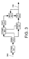
本発明の実施形態によれば、QAM信号またはPSK信号等の線形変調信号を得るために、極座標空間変調システムにおける位相変調器によって生じる位相歪みが補償される。図3に、本発明による極座標空間変調システムの一例を示す。
【0015】
図3に示すように、送信しようとする情報300(例えば2進情報)はまず、ディジタル波形フィルタ(FILTER)301でディジタル波形に変換された後、ディジタル・シグナル・プロセッサ(DSP)302で位相成分と振幅成分とに分離される。位相成分は、位相変調器(PMOD)305に送られ、ここで搬送波信号を変調し、定包絡線位相変調を得る。位相変調器は、例えばI-Q位相変調器またはΣΔフラクショナルN・PLL変調器であるが、いかなるタイプの従来の位相変調器であってもよい。このような変調器の例は、
係属中の米国特許出願第08/931,302号および米国特許出願第08/931,430号、ならびに、
T.Riley等による「簡略型連続位相変調技術(A Simplified Continuous Phase Modulator Technique)」(IEEE Transactions on Circuits and Systems-II, Vol. 41, pp. 321-326 (1994))、および、
T.Riley等による「フラクショナルn周波数合成によるΔΣ変調(Delta-sigma Modulation in Fractional-n frequency Synthesis)」(IEEE Transactions on Solid State Circuits, Vol. 28, pp. 553-559 (1993))
に開示されており、参照により本明細書に編入される。位相変調器305は位相変調された搬送波信号において位相歪みを生じる。
【0016】
この位相歪みを修正し、線形変調信号を供給するために、振幅成分が補償回路(COMP)303に送られ、ここでその振幅成分を修正して位相変調器305により生じた位相歪みを補償する。例えば、補償回路303は、位相変調器305で生じた遅延、ならびに理想位相成分および歪んだ位相成分(すなわち位相変調器により生じた位相歪みを含む位相成分)に基づいて、補償関数を導き出す。補償回路303はこの補償関数を振幅成分に適用する。補償回路303は、これらの関数の実行を、数多くの方法で実現することができる。例えば、補償回路303は、振幅成分をどのように修正するかを決定するための(例えば、補償関数を決定するための)、ルックアップテーブルと、補償関数を振幅成分に適用するための非線形ディジタルフィルタとを有することが可能である。かわりに、いくつかの関数またはすべての関数がマイクロプロセッサによって実行されるようにしてもよい。
【0017】
補償されたディジタル振幅成分は、D/Aコンバータ304でアナログ信号に変換される。得られたアナログ信号はレギュレータ(REG)307に送られ、ここでそのアナログ信号と出力信号308とに基づいてパワーアンプ306の電力を目標値に制御する信号の電流または電圧を調整する。そして、調整されたアナログ信号はパワーアンプ306において、そのパワーアンプの電力を制御することで位相変調された搬送波信号を変調し、増幅信号308が出力される。
【0018】
補償回路303がどのように動作するのかを理解するために、所望の線形変調ベースバンド信号sb(t)が、次式で表されると仮定する。
【0019】
![]()
ただし、I(t)は所望の線形変調ベースバンド信号の同相成分、Q(t)はその直交成分である。このベースバンド信号の極座標表示は、次式で与えられる。
【0021】
![]()
そして、所望の送信信号s(t)は、次式で表される。
【0023】

ただし、φtは送信しようとする信号の位相成分、r(t)は送信しようとする信号の振幅成分、ω0は搬送波周波数である。
【0025】
そして、位相変調器305からの信号出力は次式で表される。
【0026】
理想位相成分および位相変調器305からの信号出力に基づいて、補償回路303は次式で与えられる補償関数c(t)を導出する。
【0028】
ここで、q- τは遅延演算子(すなわちq- τ=x(t-τ))であり、関数A(t)は、
|c(t)|<∞,∀tとなるように、すなわち、補償関数c(t)の絶対値がすべてのtに対して無限大より小さくなるように、選択される。ω0=0のとき、すなわちベースバンド信号の場合は、式(4)が最適補償関数であることが分かる。
【0030】
Hregulator(f)=1∀f、すなわち、レギュレータの伝達関数Hregulator(f)がすべての周波数に対して1である、と仮定すると、送信信号は次式で表される。
【0031】
ただし、εtは位相誤差、すなわち、歪んだ位相成分と理想位相成分との位相歪み、を表す。εtがφtと比較して小さいと仮定し、三角恒等式およびテイラー展開を用いると、以下の関係が存在する。
【0034】
ただし、O(εt)はノイズ成分である。よって、補償された送信信号st(t)は、次式で表される。
【0036】
式(8)より、式(4)の補償関数を用いることで、送信信号は所望の信号と帯域制限された小さなノイズ成分とを有することが分かる。このノイズ成分は小さいので無視できる。したがって、補償された信号st(t)は、送信信号のための周波数スペクトル要求を満たす周波数スペクトルを有する。
【0038】
図4は、本発明による極座標空間変調システムを用いた線形変調信号を発生する方法の一例を示している。まず、ステップ400で、送信しようとする情報をフィルタリングしてディジタル波形を出力する。次に、ステップ410で、フィルタを通過した信号を振幅成分と位相成分とに分離する。ステップ420で、位相成分が搬送波信号を変調する。ステップ430で、振幅成分に例えば非線形フィルタリングを通して補償関数を適用することで振幅成分を修正して、位相変調で生じた位相歪みを補償する。ステップ440で、補償された振幅成分をアナログ信号に変換し、ステップ450で、アナログ信号と出力信号とに基づいてパワーアンプのパワーレベルを調整する。ステップ460で、位相変調された搬送波信号を振幅変調して線形変調信号を生成する。そして、線形変調信号を送信出力する。
【0039】
実施形態による装置および方法は、極座標空間変調を用いて、位相変調における位相歪みを補償することによって線形変調信号を生成する。
【0040】
本発明は、その本質的な特徴から逸脱することなく他の特定の形態によっても実現が可能であることは理解されよう。したがって、上述した実施形態は説明のためのものであってそれに限定されるものではない。
【図面の簡単な説明】
【図1A】 セルラ通信システムを示す図である。
【図1B】 従来のI-Q直交振幅変調器を示す図である。
【図2】 従来の極座標空間変調器を示す図である。
【図3】 本発明による極座標空間変調を用いて線形変調信号を発生する装置の一例を示す図である。
【図4】 本発明による極座標空間変調を用いて線形変調信号を発生する方法の一例を示す図である。[0001]
(background)
The present invention relates to a communication system using polar coordinate spatial modulation technology, and more particularly to a method and apparatus for generating a linear modulation signal using polar coordinate spatial modulation in a remote terminal of a cellular communication system.
[0002]
Recent communication systems such as cellular radio systems, satellite radio systems, etc. have various processing (analog, digital, dual mode, etc.) and access technologies (frequency division multiple access (FDMA), self and multiple access (TDMA), code Division multiple access (CDMA), or a combination of these).
[0003]
FIG. 1A is a block diagram illustrating an example of a cellular mobile radiotelephone system, including a
[0004]
In a typical transmitter, such as
[0005]
There are various modulation techniques. Quadrature amplitude modulation (QAM) and digital phase modulation (PSK) are examples of linear modulation techniques. These techniques typically use quadrature (IQ) amplitude modulation as shown in FIG. 1B. Based on the
[0006]
Another modulation technique that is often considered more efficient is polar modulation. This technique is based on a polar representation of the baseband signal and is disclosed, for example, in US Pat. No. 5,430,416 and shown in FIG. According to this technique, polar components (ie, amplitude (r) component and phase (φ) component) are used instead of the I component and the Q component. Based on the
[0007]
In order to modulate a signal that is phase modulated with an amplitude component, it is necessary to have the amplitude component phase aligned with the phase transition caused by the carrier signal. In a conventional polar coordinate space modulation device, phase distortion occurs in a component such as a power amplifier, and adjustment deviation occurs between the amplitude component and the phase-modulated carrier wave signal. The resulting amplitude component and the phase modulated carrier signal will differ from the desired modulated carrier signal.
[0008]
Various attempts have been made to solve this problem, including the technique disclosed in US Pat. No. 4,972,440. According to this patent, the phase distortion generated in the power amplifier is compensated by adding the corresponding phase distortion to the carrier signal.
[0009]
In addition to the phase distortion caused by the power amplifier, there is also phase distortion caused by a phase modulator that may include a component that functions as a low pass filter. It is assumed that the phase modulator is ideal in many cases. That is, it is assumed that the phase modulator does not cause phase distortion. However, in actual applications, the phase modulator is not ideal, and phase distortion occurs that causes a misalignment between the amplitude component and the phase modulated carrier signal. This can result in a distorted output signal having a frequency spectrum that is significantly wider than the frequency spectrum of the desired output signal. Known techniques for compensating for phase distortion caused by a power amplifier cannot solve the problem of phase distortion caused by a phase modulator.
[0010]
Therefore, there is a need for a method and apparatus that compensates for phase distortion caused by phase modulation in a polar coordinate spatial modulation system.
[0011]
(Overview)
In view of the above, an object of the present invention is to compensate for phase distortion caused by phase modulation in a polar coordinate spatial modulation system and provide a linear modulation signal. Another object of the present invention is to meet the spectral requirements for signal transmission utilizing the efficiency of polar spatial modulation.
[0012]
According to embodiments, these and other objectives are achieved by an apparatus and method for generating a linear modulation signal (eg, a QAM signal or a PSK signal) in a polar spatial modulation system. A signal for transmission is separated into a phase component and an amplitude component, and the carrier signal is phase-modulated with the phase component. The phase modulator produces phase distortion that is compensated for correction of the amplitude component. The phase modulated signal is amplitude modulated by the compensated amplitude component to produce a linearly modulated signal.
[0013]
(Detailed explanation)
For illustrative purposes, a cellular wireless communication system is shown in the following description, but it will be understood that the present invention is not limited thereto and is applicable to other types of communication systems.
[0014]
According to embodiments of the present invention, phase distortion caused by a phase modulator in a polar spatial modulation system is compensated to obtain a linear modulation signal such as a QAM signal or a PSK signal. FIG. 3 shows an example of a polar coordinate spatial modulation system according to the present invention.
[0015]
As shown in FIG. 3, information 300 (for example, binary information) to be transmitted is first converted into a digital waveform by a digital waveform filter (FILTER) 301 and then phase components by a digital signal processor (DSP) 302. And amplitude components. The phase component is sent to a phase modulator (PMOD) 305, where the carrier signal is modulated to obtain constant envelope phase modulation. The phase modulator is, for example, an IQ phase modulator or a ΣΔ fractional N · PLL modulator, but may be any type of conventional phase modulator. Examples of such modulators are
Pending U.S. patent application Ser.No. 08 / 931,302 and U.S. patent application Ser.No. 08 / 931,430, and
“A Simplified Continuous Phase Modulator Technique” by T. Riley et al. (IEEE Transactions on Circuits and Systems-II, Vol. 41, pp. 321-326 (1994)), and
T.Riley et al. “Delta-sigma Modulation in Fractional-n Frequency Synthesis” (IEEE Transactions on Solid State Circuits, Vol. 28, pp. 553-559 (1993))
And is incorporated herein by reference.
[0016]
In order to correct this phase distortion and provide a linearly modulated signal, the amplitude component is sent to a compensation circuit (COMP) 303 where it is corrected to compensate for the phase distortion caused by the
[0017]
The compensated digital amplitude component is converted into an analog signal by the D /
[0018]
To understand how the
[0019]
![]()
Where I (t) is the in-phase component of the desired linear modulation baseband signal and Q (t) is its quadrature component. The polar coordinate display of this baseband signal is given by
[0021]
![]()
The desired transmission signal s (t) is expressed by the following equation.
[0023]
Where φ t is the phase component of the signal to be transmitted, r (t) is the amplitude component of the signal to be transmitted, and ω 0 is the carrier frequency.
[0025]
The signal output from the
[0026]
Based on the ideal phase component and the signal output from the
[0028]
Where q - τ is a delay operator (ie q - τ = x (t-τ)) and the function A (t) is
| C (t) | <∞, ∀t, that is, the absolute value of the compensation function c (t) is selected to be smaller than infinity for all t. When ω 0 = 0, that is, in the case of a baseband signal, it can be seen that Equation (4) is an optimal compensation function.
[0030]
Assuming that H regulator (f) = 1∀f, that is, the regulator transfer function H regulator (f) is 1 for all frequencies, the transmitted signal is expressed as:
[0031]
Here, ε t represents a phase error, that is, a phase distortion between a distorted phase component and an ideal phase component. Assuming that ε t is small compared to φ t and using the triangle identity and Taylor expansion, the following relationship exists:
[0034]
However, O (ε t ) is a noise component. Therefore, the compensated transmission signal s t (t) is expressed by the following equation.
[0036]
From equation (8), it can be seen that by using the compensation function of equation (4), the transmission signal has a desired signal and a small noise component that is band-limited. This noise component is small and can be ignored. Thus, the compensated signal s t (t) has a frequency spectrum that satisfies the frequency spectrum requirements for the transmitted signal.
[0038]
FIG. 4 shows an example of a method for generating a linear modulation signal using a polar spatial modulation system according to the present invention. First, in
[0039]
Apparatuses and methods according to embodiments use linear spatial modulation to generate a linear modulation signal by compensating for phase distortion in phase modulation.
[0040]
It will be appreciated that the invention may be practiced in other specific forms without departing from its essential characteristics. Therefore, the above-described embodiment is for explanation and is not limited thereto.
[Brief description of the drawings]
FIG. 1A shows a cellular communication system.
FIG. 1B shows a conventional IQ quadrature amplitude modulator.
FIG. 2 is a diagram showing a conventional polar coordinate spatial modulator.
FIG. 3 shows an example of an apparatus for generating a linear modulation signal using polar coordinate spatial modulation according to the present invention.
FIG. 4 is a diagram illustrating an example of a method for generating a linear modulation signal using polar coordinate spatial modulation according to the present invention.
Claims (10)
送信のための信号を位相成分と振幅成分とに分離するシグナルプロセッサと、
前記位相成分で搬送波信号を変調する位相変調器と、
前記振幅成分で前記位相変調された搬送波信号を変調して線形変調信号を生成する振幅変調器と、
前記位相変調器によって生じた位相歪みを補償する補償回路と、
を備え、
前記補償回路は、前記位相成分を入力するように前記シグナルプロセッサに接続されるとともに、前記位相変調器で生じた遅延を表す信号及び歪んだ位相成分の情報を受信するように前記位相変調器に接続される
ことを特徴とする装置。An apparatus for generating a linear modulation signal in a polar spatial modulation system comprising:
A signal processor for separating a signal for transmission into a phase component and an amplitude component;
A phase modulator that modulates a carrier signal with the phase component;
An amplitude modulator that modulates the phase-modulated carrier signal with the amplitude component to generate a linearly modulated signal;
A compensation circuit for compensating for phase distortion caused by the phase modulator;
Equipped with a,
The compensation circuit is connected to the signal processor to input the phase component, and to the phase modulator to receive a signal representing a delay caused by the phase modulator and information on the distorted phase component. A device characterized by being connected .
前記補償回路は、補償関数c(t)を、
The compensation circuit calculates a compensation function c (t),
送信のための信号を位相成分と振幅成分とに分離する分離ステップと、
位相変調器が、前記位相成分で搬送波信号を位相変調する位相変調ステップと、
振幅変調器が、前記振幅成分で前記位相変調された搬送波信号を変調する振幅変調ステップと、
補償回路が、前記位相変調によって生じた位相歪みを補償する補償ステップと、
を有し、
前記位相変調器で生じた遅延を表す信号及び歪んだ位相成分の情報に依存して、前記位相変調器から前記補償回路に信号が転送される
ことを特徴とする方法。A method for generating a linear modulation signal in a polar spatial modulation system comprising:
A separation step of separating a signal for transmission into a phase component and an amplitude component;
Phase modulator, a phase modulating step of phase modulating the carrier signal with the phase component,
And amplitude modulation step amplitude modulator for modulating the phase modulated carrier signal with the amplitude component,
A compensation step in which a compensation circuit compensates for phase distortion caused by the phase modulation;
I have a,
A method in which a signal is transferred from the phase modulator to the compensation circuit depending on a signal representing a delay caused by the phase modulator and information on a distorted phase component .
前記補償回路において、補償関数c(t)が、
In the compensation circuit, the compensation function c (t) is
Applications Claiming Priority (3)
| Application Number | Priority Date | Filing Date | Title |
|---|---|---|---|
| US09/167,658 | 1998-10-07 | ||
| US09/167,658 US6101224A (en) | 1998-10-07 | 1998-10-07 | Method and apparatus for generating a linearly modulated signal using polar modulation |
| PCT/SE1999/001790 WO2000021191A1 (en) | 1998-10-07 | 1999-10-06 | Method and apparatus for generating a linearly modulated signal using polar modulation |
Publications (3)
| Publication Number | Publication Date |
|---|---|
| JP2002527921A JP2002527921A (en) | 2002-08-27 |
| JP2002527921A5 JP2002527921A5 (en) | 2006-11-24 |
| JP4414100B2 true JP4414100B2 (en) | 2010-02-10 |
Family
ID=22608259
Family Applications (1)
| Application Number | Title | Priority Date | Filing Date |
|---|---|---|---|
| JP2000575213A Expired - Fee Related JP4414100B2 (en) | 1998-10-07 | 1999-10-06 | Method and apparatus for generating a linearly modulated signal using polar coordinate spatial modulation |
Country Status (9)
| Country | Link |
|---|---|
| US (1) | US6101224A (en) |
| EP (1) | EP1119902B1 (en) |
| JP (1) | JP4414100B2 (en) |
| CN (1) | CN1130817C (en) |
| AT (1) | ATE247876T1 (en) |
| AU (1) | AU1304800A (en) |
| DE (1) | DE69910599T2 (en) |
| MY (1) | MY126431A (en) |
| WO (1) | WO2000021191A1 (en) |
Families Citing this family (101)
| Publication number | Priority date | Publication date | Assignee | Title |
|---|---|---|---|---|
| EP1010306A1 (en) * | 1997-08-25 | 2000-06-21 | Nokia Corporation | Digital modulator for angle and/or amplitude modulation |
| US7548787B2 (en) * | 2005-08-03 | 2009-06-16 | Kamilo Feher | Medical diagnostic and communication system |
| US6757334B1 (en) * | 1998-08-10 | 2004-06-29 | Kamilo Feher | Bit rate agile third-generation wireless CDMA, GSM, TDMA and OFDM system |
| US7079584B2 (en) * | 1998-08-10 | 2006-07-18 | Kamilo Feher | OFDM, CDMA, spread spectrum, TDMA, cross-correlated and filtered modulation |
| US8050345B1 (en) | 1999-08-09 | 2011-11-01 | Kamilo Feher | QAM and GMSK systems |
| US6470055B1 (en) * | 1998-08-10 | 2002-10-22 | Kamilo Feher | Spectrally efficient FQPSK, FGMSK, and FQAM for enhanced performance CDMA, TDMA, GSM, OFDN, and other systems |
| US7593481B2 (en) * | 1998-08-31 | 2009-09-22 | Kamilo Feher | CDMA, W-CDMA, 3rd generation interoperable modem format selectable (MFS) systems with GMSK modulated systems |
| US7415066B2 (en) * | 1998-08-10 | 2008-08-19 | Kamilo Feher | Mis-matched modulation-demodulation format selectable filters |
| US6198777B1 (en) | 1998-08-31 | 2001-03-06 | Kamilo Feher | Feher keying (KF) modualtion and transceivers including clock shaping processors |
| US6377784B2 (en) * | 1999-02-09 | 2002-04-23 | Tropian, Inc. | High-efficiency modulation RF amplifier |
| US6864668B1 (en) | 1999-02-09 | 2005-03-08 | Tropian, Inc. | High-efficiency amplifier output level and burst control |
| US6490440B1 (en) * | 1999-06-01 | 2002-12-03 | Motorola, Inc. | Digital transmitter circuit and method of operation |
| US9373251B2 (en) | 1999-08-09 | 2016-06-21 | Kamilo Feher | Base station devices and automobile wireless communication systems |
| US9813270B2 (en) | 1999-08-09 | 2017-11-07 | Kamilo Feher | Heart rate sensor and medical diagnostics wireless devices |
| US7260369B2 (en) | 2005-08-03 | 2007-08-21 | Kamilo Feher | Location finder, tracker, communication and remote control system |
| US9307407B1 (en) | 1999-08-09 | 2016-04-05 | Kamilo Feher | DNA and fingerprint authentication of mobile devices |
| US6366177B1 (en) | 2000-02-02 | 2002-04-02 | Tropian Inc. | High-efficiency power modulators |
| DE10056472A1 (en) * | 2000-11-15 | 2002-05-29 | Infineon Technologies Ag | Polar loop transmission circuit has oscillator producing HF signal depending on phase comparison, amplitude modulator, feedback path, amplifier between amplitude modulator, mixer |
| US6754287B2 (en) * | 2001-03-21 | 2004-06-22 | Skyworks Solutions, Inc. | Method and apparatus for producing a modulated signal |
| US7020070B2 (en) | 2001-04-10 | 2006-03-28 | Telefonaktiebolaget L M Ericsson (Publ) | Selectively controlled modulation distortion of an IQ-baseband signal |
| US6701138B2 (en) * | 2001-06-11 | 2004-03-02 | Rf Micro Devices, Inc. | Power amplifier control |
| US20070060074A1 (en) * | 2002-03-07 | 2007-03-15 | Matsushita Electric Industrial Co., Ltd. | High-efficiency modulating RF amplifier |
| US6834084B2 (en) * | 2002-05-06 | 2004-12-21 | Rf Micro Devices Inc | Direct digital polar modulator |
| US7991071B2 (en) * | 2002-05-16 | 2011-08-02 | Rf Micro Devices, Inc. | AM to PM correction system for polar modulator |
| US7801244B2 (en) * | 2002-05-16 | 2010-09-21 | Rf Micro Devices, Inc. | Am to AM correction system for polar modulator |
| US6892057B2 (en) * | 2002-08-08 | 2005-05-10 | Telefonaktiebolaget Lm Ericsson (Publ) | Method and apparatus for reducing dynamic range of a power amplifier |
| US7551685B2 (en) * | 2003-08-25 | 2009-06-23 | M/A-Com, Inc. | Apparatus, methods and articles of manufacture for signal correction using adaptive phase re-alignment |
| US7545865B2 (en) * | 2002-12-03 | 2009-06-09 | M/A-Com, Inc. | Apparatus, methods and articles of manufacture for wideband signal processing |
| US7187231B2 (en) * | 2002-12-02 | 2007-03-06 | M/A-Com, Inc. | Apparatus, methods and articles of manufacture for multiband signal processing |
| US6891432B2 (en) * | 2002-11-14 | 2005-05-10 | Mia-Com, Inc. | Apparatus, methods and articles of manufacture for electromagnetic processing |
| US7502422B2 (en) * | 2003-06-04 | 2009-03-10 | M/A—COM, Inc. | Electromagnetic wave transmitter systems, methods and articles of manufacture |
| US7245183B2 (en) * | 2002-11-14 | 2007-07-17 | M/A-Com Eurotec Bv | Apparatus, methods and articles of manufacture for processing an electromagnetic wave |
| US7203262B2 (en) | 2003-05-13 | 2007-04-10 | M/A-Com, Inc. | Methods and apparatus for signal modification in a fractional-N phase locked loop system |
| US6924699B2 (en) * | 2003-03-06 | 2005-08-02 | M/A-Com, Inc. | Apparatus, methods and articles of manufacture for digital modification in electromagnetic signal processing |
| US7526260B2 (en) * | 2002-11-14 | 2009-04-28 | M/A-Com Eurotec, B.V. | Apparatus, methods and articles of manufacture for linear signal modification |
| US7298854B2 (en) * | 2002-12-04 | 2007-11-20 | M/A-Com, Inc. | Apparatus, methods and articles of manufacture for noise reduction in electromagnetic signal processing |
| US6701134B1 (en) * | 2002-11-05 | 2004-03-02 | Rf Micro Devices, Inc. | Increased dynamic range for power amplifiers used with polar modulation |
| JP2004175052A (en) * | 2002-11-29 | 2004-06-24 | Sony Corp | Medium to be recorded by ink jetting, ink jet imaging method, and printed matter |
| US6859098B2 (en) | 2003-01-17 | 2005-02-22 | M/A-Com, Inc. | Apparatus, methods and articles of manufacture for control in an electromagnetic processor |
| US7447272B2 (en) * | 2003-04-22 | 2008-11-04 | Freescale Semiconductor, Inc. | Filter method and apparatus for polar modulation |
| GB2402006B (en) * | 2003-05-23 | 2005-08-10 | Motorola Inc | Analog to digital converter |
| US7043213B2 (en) * | 2003-06-24 | 2006-05-09 | Northrop Grumman Corporation | Multi-mode amplifier system |
| US6987417B2 (en) * | 2003-06-24 | 2006-01-17 | Northrop Grumman Corpoation | Polar and linear amplifier system |
| US7251462B2 (en) * | 2003-07-08 | 2007-07-31 | Matsushita Electric Industrial Co., Ltd. | Modulation circuit device, modulation method and radio communication device |
| US7126999B2 (en) * | 2003-08-11 | 2006-10-24 | Telefonaktiebolaget Lm Ericsson (Publ) | Pseudo-polar modulation for radio transmitters |
| WO2005027297A2 (en) * | 2003-09-16 | 2005-03-24 | Nokia Corporation | Hybrid switched mode/linear power amplifier power supply for use in polar transmitter |
| US7480511B2 (en) * | 2003-09-19 | 2009-01-20 | Trimble Navigation Limited | Method and system for delivering virtual reference station data |
| US7091778B2 (en) * | 2003-09-19 | 2006-08-15 | M/A-Com, Inc. | Adaptive wideband digital amplifier for linearly modulated signal amplification and transmission |
| JP3935460B2 (en) * | 2003-09-30 | 2007-06-20 | 松下電器産業株式会社 | Amplitude information extraction apparatus and amplitude information extraction method |
| JP4395044B2 (en) * | 2003-10-22 | 2010-01-06 | パナソニック株式会社 | Modulation apparatus and modulation method |
| US7343138B2 (en) * | 2003-12-08 | 2008-03-11 | M/A-Com, Inc. | Compensating for load pull in electromagentic signal propagation using adaptive impedance matching |
| US7912145B2 (en) * | 2003-12-15 | 2011-03-22 | Marvell World Trade Ltd. | Filter for a modulator and methods thereof |
| JP3961498B2 (en) * | 2004-02-27 | 2007-08-22 | 松下電器産業株式会社 | High frequency circuit equipment |
| CN1930784B (en) * | 2004-03-10 | 2010-06-09 | 松下电器产业株式会社 | Transmission device and radio communication device |
| US7551686B1 (en) | 2004-06-23 | 2009-06-23 | Rf Micro Devices, Inc. | Multiple polynomial digital predistortion |
| US8031028B2 (en) * | 2004-07-07 | 2011-10-04 | SiGe Semiconductor (Europe) Ltd. | Polar signal processor to drive a segmented power amplifier and method therefore |
| US7109791B1 (en) * | 2004-07-09 | 2006-09-19 | Rf Micro Devices, Inc. | Tailored collector voltage to minimize variation in AM to PM distortion in a power amplifier |
| US7529523B1 (en) | 2004-08-23 | 2009-05-05 | Rf Micro Devices, Inc. | N-th order curve fit for power calibration in a mobile terminal |
| US7359680B2 (en) * | 2004-09-14 | 2008-04-15 | Telefonaktiebolaget Lm Ericsson (Publ) | Delay calibration in polar modulation transmitters |
| US7983632B2 (en) * | 2004-09-24 | 2011-07-19 | Broadcom Corporation | Feedback control loop for amplitude modulation in a polar transmitter with a translational loop |
| US7359449B2 (en) * | 2004-10-05 | 2008-04-15 | Kamilo Feher | Data communication for wired and wireless communication |
| US7596185B2 (en) | 2004-12-13 | 2009-09-29 | Infineon Technologies Ag | Radio transmitter with variable amplifier units in the baseband section and in the radio-frequency section of the transmission path |
| DE102004059985B4 (en) * | 2004-12-13 | 2017-11-16 | Intel Deutschland Gmbh | Radio transmitter with adjustable amplifier units in the baseband and in the high-frequency section of the transmission path |
| EP1875702B1 (en) * | 2005-04-27 | 2009-02-04 | Panasonic Corporation | Polar modulation transmission circuit and communication device |
| US7336127B2 (en) * | 2005-06-10 | 2008-02-26 | Rf Micro Devices, Inc. | Doherty amplifier configuration for a collector controlled power amplifier |
| US8224265B1 (en) | 2005-06-13 | 2012-07-17 | Rf Micro Devices, Inc. | Method for optimizing AM/AM and AM/PM predistortion in a mobile terminal |
| US20070018718A1 (en) * | 2005-06-20 | 2007-01-25 | National Sun Yat-Sen University | Microwave transmitter and the method for increasing envelope bandwidth |
| US7493097B2 (en) * | 2005-07-07 | 2009-02-17 | Skyworks Solutions, Inc. | High dynamic range compact mixer output stage for a wireless receiver |
| US20070015472A1 (en) * | 2005-07-15 | 2007-01-18 | Simo Murtojarvi | Multimode transmitter, module, communication device and chip set |
| US20070018701A1 (en) * | 2005-07-20 | 2007-01-25 | M/A-Com, Inc. | Charge pump apparatus, system, and method |
| US10009956B1 (en) | 2017-09-02 | 2018-06-26 | Kamilo Feher | OFDM, 3G and 4G cellular multimode systems and wireless mobile networks |
| US7280810B2 (en) | 2005-08-03 | 2007-10-09 | Kamilo Feher | Multimode communication system |
| US20070087770A1 (en) * | 2005-10-14 | 2007-04-19 | Hong Gan | Methods and apparatuses for transmission power control in a wireless communication system |
| US7330071B1 (en) | 2005-10-19 | 2008-02-12 | Rf Micro Devices, Inc. | High efficiency radio frequency power amplifier having an extended dynamic range |
| JP4584336B2 (en) * | 2005-10-21 | 2010-11-17 | エヌエックスピー ビー ヴィ | Polar modulation apparatus and method using FM modulation |
| US7483680B2 (en) * | 2005-12-20 | 2009-01-27 | Telefonaktiebolaget Lm Ericsson (Publ) | Method and apparatus for modulation path delay mismatch compensation in a polar modulation transmitter |
| US8884714B2 (en) * | 2005-12-22 | 2014-11-11 | Pine Valley Investments, Inc. | Apparatus, system, and method for digital base modulation of power amplifier in polar transmitter |
| US7599448B2 (en) * | 2006-02-03 | 2009-10-06 | Pine Valley Investments, Inc. | Multi-mode selectable modulation architecture calibration and power control apparatus, system, and method for radio frequency power amplifier |
| US7877060B1 (en) | 2006-02-06 | 2011-01-25 | Rf Micro Devices, Inc. | Fast calibration of AM/PM pre-distortion |
| US7522676B2 (en) * | 2006-02-06 | 2009-04-21 | Nokia Corporation | Method and system for transmitter envelope delay calibration |
| JP4469347B2 (en) * | 2006-02-28 | 2010-05-26 | パナソニック株式会社 | Polar coordinate modulator |
| US20070216455A1 (en) * | 2006-03-17 | 2007-09-20 | M/A-Com, Inc. | Partial cascode delay locked loop architecture |
| US7962108B1 (en) | 2006-03-29 | 2011-06-14 | Rf Micro Devices, Inc. | Adaptive AM/PM compensation |
| US7596184B2 (en) * | 2006-03-30 | 2009-09-29 | Pine Valley Investments, Inc. | Apparatus, system, and method for amplitude-phase synchronization in polar transmitter |
| US7471154B2 (en) | 2006-08-08 | 2008-12-30 | Skyworks Solutions, Inc. | Bias circuit for maintaining high linearity at cutback power conditions |
| US7446612B2 (en) * | 2006-09-08 | 2008-11-04 | Skyworks Solutions, Inc. | Amplifier feedback and bias configuration |
| US7830220B2 (en) * | 2006-09-26 | 2010-11-09 | Infineon Technologies Ag | Modulator arrangement and method for signal modulation |
| US7689182B1 (en) | 2006-10-12 | 2010-03-30 | Rf Micro Devices, Inc. | Temperature compensated bias for AM/PM improvement |
| US7696826B2 (en) * | 2006-12-04 | 2010-04-13 | Skyworks Solutions, Inc. | Temperature compensation of collector-voltage control RF amplifiers |
| US8009765B2 (en) * | 2007-03-13 | 2011-08-30 | Pine Valley Investments, Inc. | Digital polar transmitter |
| US8009762B1 (en) | 2007-04-17 | 2011-08-30 | Rf Micro Devices, Inc. | Method for calibrating a phase distortion compensated polar modulated radio frequency transmitter |
| US7991366B2 (en) * | 2008-05-20 | 2011-08-02 | Panasonic Corporation | Methods and apparatus for reconstructing amplitude modulation signals in polar modulation transmitters |
| US8229029B2 (en) * | 2009-01-14 | 2012-07-24 | Harris Corporation | Transmitter with reduced spectral regrowth and associated methods |
| US8489042B1 (en) | 2009-10-08 | 2013-07-16 | Rf Micro Devices, Inc. | Polar feedback linearization |
| US8195102B2 (en) * | 2010-06-02 | 2012-06-05 | Nxp B.V. | System and method for transmitting a baseband real signal with a non-constant envelope using a polar transmitter |
| US8325073B2 (en) * | 2010-11-30 | 2012-12-04 | Qualcomm Incorporated | Performing enhanced sigma-delta modulation |
| US8798194B2 (en) * | 2011-12-15 | 2014-08-05 | Intel Mobile Communications GmbH | Adaptive compensation of nonlinear frequency distortion in polar transmitters based on a least squares estimation |
| US8638878B2 (en) * | 2011-12-15 | 2014-01-28 | Intel Mobile Communications GmbH | Method and faculty to measure and compensate DCO frequency distortions using a DPLL |
| US8867660B2 (en) | 2011-12-15 | 2014-10-21 | Intel Mobile Communications GmbH | Method and system to measure and compensate undue DCO frequency peaks at GFSK ramp down |
| US9172570B1 (en) | 2014-06-13 | 2015-10-27 | Intel IP Corporation | Compensation of oscillator frequency pulling |
| US9923529B2 (en) | 2016-02-03 | 2018-03-20 | Samsung Electronics Co., Ltd | Customizable ramp-up and ramp-down amplitude profiles for a digital power amplifier (DPA) based transmitter |
Family Cites Families (24)
| Publication number | Priority date | Publication date | Assignee | Title |
|---|---|---|---|---|
| GB918583A (en) * | 1958-03-27 | 1900-01-01 | ||
| US3906401A (en) * | 1974-09-03 | 1975-09-16 | Bell Telephone Labor Inc | Feedforward error correction in interferometer modulators |
| US4324952A (en) * | 1978-08-21 | 1982-04-13 | Harris Corporation | Direct function receivers and transmitters for multichannel communications system |
| US4268802A (en) * | 1979-05-23 | 1981-05-19 | Fisher Charles B | Modulation distortion reducer |
| US4373115A (en) * | 1980-08-18 | 1983-02-08 | Kahn Leonard R | Predictive distortion reduction in AM stereo transmitters |
| US4509017A (en) * | 1981-09-28 | 1985-04-02 | E-Systems, Inc. | Method and apparatus for pulse angle modulation |
| US4485358A (en) * | 1981-09-28 | 1984-11-27 | E-Systems, Inc. | Method and apparatus for pulse angle modulation |
| US4584541A (en) * | 1984-12-28 | 1986-04-22 | Rca Corporation | Digital modulator with variations of phase and amplitude modulation |
| US4700151A (en) * | 1985-03-20 | 1987-10-13 | Nec Corporation | Modulation system capable of improving a transmission system |
| IT1215370B (en) * | 1987-02-26 | 1990-02-08 | Gtg Ora Siemens Telecomunicazi | LINEARIZER FOR MICROWAVE POWER AMPLIFIER. |
| US4972440A (en) * | 1988-09-23 | 1990-11-20 | Hughes Aircraft Company | Transmitter circuit for efficiently transmitting communication traffic via phase modulated carrier signals |
| US4968956A (en) * | 1989-12-04 | 1990-11-06 | Trw Inc. | Microwave phase modulator having a quadrature path with phase offset |
| GB9002789D0 (en) * | 1990-02-08 | 1990-04-04 | Marconi Co Ltd | Circuit for reducing distortion produced by an r.f.power amplifier |
| IT1251082B (en) * | 1991-07-11 | 1995-05-04 | Sits Soc It Telecom Siemens | PROCEDURE FOR THE COMPENSATION OF THE AM / PM DISTORTION OF A TRANSMITTER THROUGH MODULATION OF THE PHASE OF THE GLOCAL OSCILLATION, AND RELATED CIRCUIT OF COMPEMSATION. |
| JPH05152981A (en) * | 1991-11-26 | 1993-06-18 | Iwatsu Electric Co Ltd | Receiver for composite modulation wave |
| JP3166321B2 (en) * | 1992-07-01 | 2001-05-14 | 日本電気株式会社 | Modulated signal transmission system |
| US5450044A (en) * | 1993-04-14 | 1995-09-12 | Acrodyne Industries, Inc. | Quadrature amplitude modulator including a digital amplitude modulator as a component thereof |
| US5420536A (en) * | 1993-03-16 | 1995-05-30 | Victoria University Of Technology | Linearized power amplifier |
| US5430416A (en) * | 1994-02-23 | 1995-07-04 | Motorola | Power amplifier having nested amplitude modulation controller and phase modulation controller |
| US5506546A (en) * | 1994-06-20 | 1996-04-09 | Nec Corporation | Method and apparatus for generating transmitting wave |
| JP2964883B2 (en) * | 1994-09-30 | 1999-10-18 | 日本電気株式会社 | Transmitter |
| US5491454A (en) * | 1994-10-31 | 1996-02-13 | Motorola, Inc. | Method and apparatus for reducing distortion in an output signal of an amplifier |
| JP3560398B2 (en) * | 1995-08-31 | 2004-09-02 | 富士通株式会社 | Amplifier with distortion compensation |
| US5705959A (en) * | 1996-10-08 | 1998-01-06 | The United States Of America As Represented By The Secretary Of The Air Force | High efficiency low distortion amplification |
-
1998
- 1998-10-07 US US09/167,658 patent/US6101224A/en not_active Expired - Lifetime
-
1999
- 1999-10-06 JP JP2000575213A patent/JP4414100B2/en not_active Expired - Fee Related
- 1999-10-06 MY MYPI99004302A patent/MY126431A/en unknown
- 1999-10-06 DE DE69910599T patent/DE69910599T2/en not_active Expired - Lifetime
- 1999-10-06 CN CN99811811.7A patent/CN1130817C/en not_active Expired - Fee Related
- 1999-10-06 EP EP99956435A patent/EP1119902B1/en not_active Expired - Lifetime
- 1999-10-06 AT AT99956435T patent/ATE247876T1/en not_active IP Right Cessation
- 1999-10-06 WO PCT/SE1999/001790 patent/WO2000021191A1/en active IP Right Grant
- 1999-10-06 AU AU13048/00A patent/AU1304800A/en not_active Abandoned
Also Published As
| Publication number | Publication date |
|---|---|
| ATE247876T1 (en) | 2003-09-15 |
| WO2000021191A1 (en) | 2000-04-13 |
| CN1322398A (en) | 2001-11-14 |
| AU1304800A (en) | 2000-04-26 |
| EP1119902A1 (en) | 2001-08-01 |
| MY126431A (en) | 2006-09-29 |
| DE69910599T2 (en) | 2004-06-24 |
| US6101224A (en) | 2000-08-08 |
| EP1119902B1 (en) | 2003-08-20 |
| CN1130817C (en) | 2003-12-10 |
| DE69910599D1 (en) | 2003-09-25 |
| JP2002527921A (en) | 2002-08-27 |
Similar Documents
| Publication | Publication Date | Title |
|---|---|---|
| JP4414100B2 (en) | Method and apparatus for generating a linearly modulated signal using polar coordinate spatial modulation | |
| US6834084B2 (en) | Direct digital polar modulator | |
| US7346122B1 (en) | Direct modulation of a power amplifier with adaptive digital predistortion | |
| US7010280B1 (en) | Linear RF power amplifier and transmitter | |
| US7068984B2 (en) | Systems and methods for amplification of a communication signal | |
| US7230996B2 (en) | Transmitting circuit device and wireless communications device | |
| US7288999B1 (en) | Pre-distortion system for a synthesizer having modulation applied in the reference path | |
| US8565338B2 (en) | High bandwidth modulation and transmission | |
| JP2000286915A (en) | Signal modulation circuit and method | |
| US7751496B2 (en) | Electromagnetic wave transmitter, receiver and transceiver systems, methods and articles of manufacture | |
| JPWO2005011109A1 (en) | Amplification equipment | |
| US6836646B2 (en) | Circuit and method for compensating for non-linear distortion | |
| US6415002B1 (en) | Phase and amplitude modulation of baseband signals | |
| US7474708B1 (en) | Multimode transmitter architecture | |
| US7024167B2 (en) | Method for amplitude modulation of a radio frequency signal, and device therefor | |
| US7221915B2 (en) | Electromagnetic wave transmitter, receiver and transceiver systems, methods and articles of manufacture | |
| JP2009513053A (en) | Polar modulation apparatus and method using FM modulation | |
| JP2009509424A (en) | Method and apparatus for baseband compensation of offset phase locked loop | |
| US6870435B2 (en) | Electromagnetic wave transmitter, receiver and transceiver systems, methods and articles of manufacture | |
| US7474878B1 (en) | Closed loop polar modulation system with open loop option at low power levels | |
| JPH0831886B2 (en) | Transmitter | |
| JPH11196140A (en) | Power amplifier | |
| JP2004504772A (en) | Reference signal predistortion for transmitters with phase coding based on frequency synthesizer | |
| WO2004034667A2 (en) | Electromagnetic wave trasmitter systems, methods and articles of manufacture | |
| WO2004036737A2 (en) | Transmitter |
Legal Events
| Date | Code | Title | Description |
|---|---|---|---|
| A521 | Request for written amendment filed |
Free format text: JAPANESE INTERMEDIATE CODE: A523 Effective date: 20060929 |
|
| A621 | Written request for application examination |
Free format text: JAPANESE INTERMEDIATE CODE: A621 Effective date: 20060929 |
|
| A977 | Report on retrieval |
Free format text: JAPANESE INTERMEDIATE CODE: A971007 Effective date: 20090529 |
|
| A131 | Notification of reasons for refusal |
Free format text: JAPANESE INTERMEDIATE CODE: A131 Effective date: 20090608 |
|
| A521 | Request for written amendment filed |
Free format text: JAPANESE INTERMEDIATE CODE: A523 Effective date: 20090907 |
|
| TRDD | Decision of grant or rejection written | ||
| A01 | Written decision to grant a patent or to grant a registration (utility model) |
Free format text: JAPANESE INTERMEDIATE CODE: A01 Effective date: 20091023 |
|
| A01 | Written decision to grant a patent or to grant a registration (utility model) |
Free format text: JAPANESE INTERMEDIATE CODE: A01 |
|
| A61 | First payment of annual fees (during grant procedure) |
Free format text: JAPANESE INTERMEDIATE CODE: A61 Effective date: 20091119 |
|
| FPAY | Renewal fee payment (event date is renewal date of database) |
Free format text: PAYMENT UNTIL: 20121127 Year of fee payment: 3 |
|
| R150 | Certificate of patent or registration of utility model |
Free format text: JAPANESE INTERMEDIATE CODE: R150 |
|
| FPAY | Renewal fee payment (event date is renewal date of database) |
Free format text: PAYMENT UNTIL: 20131127 Year of fee payment: 4 |
|
| R250 | Receipt of annual fees |
Free format text: JAPANESE INTERMEDIATE CODE: R250 |
|
| S111 | Request for change of ownership or part of ownership |
Free format text: JAPANESE INTERMEDIATE CODE: R313113 |
|
| S111 | Request for change of ownership or part of ownership |
Free format text: JAPANESE INTERMEDIATE CODE: R313113 |
|
| R350 | Written notification of registration of transfer |
Free format text: JAPANESE INTERMEDIATE CODE: R350 |
|
| R250 | Receipt of annual fees |
Free format text: JAPANESE INTERMEDIATE CODE: R250 |
|
| R250 | Receipt of annual fees |
Free format text: JAPANESE INTERMEDIATE CODE: R250 |
|
| R250 | Receipt of annual fees |
Free format text: JAPANESE INTERMEDIATE CODE: R250 |
|
| LAPS | Cancellation because of no payment of annual fees |