JP4411100B2 - Exposure equipment - Google Patents
Exposure equipment Download PDFInfo
- Publication number
- JP4411100B2 JP4411100B2 JP2004040977A JP2004040977A JP4411100B2 JP 4411100 B2 JP4411100 B2 JP 4411100B2 JP 2004040977 A JP2004040977 A JP 2004040977A JP 2004040977 A JP2004040977 A JP 2004040977A JP 4411100 B2 JP4411100 B2 JP 4411100B2
- Authority
- JP
- Japan
- Prior art keywords
- original
- contact
- holding
- reticle
- exposure apparatus
- Prior art date
- Legal status (The legal status is an assumption and is not a legal conclusion. Google has not performed a legal analysis and makes no representation as to the accuracy of the status listed.)
- Expired - Fee Related
Links
Images


Classifications
-
- G—PHYSICS
- G03—PHOTOGRAPHY; CINEMATOGRAPHY; ANALOGOUS TECHNIQUES USING WAVES OTHER THAN OPTICAL WAVES; ELECTROGRAPHY; HOLOGRAPHY
- G03F—PHOTOMECHANICAL PRODUCTION OF TEXTURED OR PATTERNED SURFACES, e.g. FOR PRINTING, FOR PROCESSING OF SEMICONDUCTOR DEVICES; MATERIALS THEREFOR; ORIGINALS THEREFOR; APPARATUS SPECIALLY ADAPTED THEREFOR
- G03F7/00—Photomechanical, e.g. photolithographic, production of textured or patterned surfaces, e.g. printing surfaces; Materials therefor, e.g. comprising photoresists; Apparatus specially adapted therefor
- G03F7/70—Microphotolithographic exposure; Apparatus therefor
- G03F7/70691—Handling of masks or workpieces
- G03F7/707—Chucks, e.g. chucking or un-chucking operations or structural details
-
- G—PHYSICS
- G03—PHOTOGRAPHY; CINEMATOGRAPHY; ANALOGOUS TECHNIQUES USING WAVES OTHER THAN OPTICAL WAVES; ELECTROGRAPHY; HOLOGRAPHY
- G03F—PHOTOMECHANICAL PRODUCTION OF TEXTURED OR PATTERNED SURFACES, e.g. FOR PRINTING, FOR PROCESSING OF SEMICONDUCTOR DEVICES; MATERIALS THEREFOR; ORIGINALS THEREFOR; APPARATUS SPECIALLY ADAPTED THEREFOR
- G03F7/00—Photomechanical, e.g. photolithographic, production of textured or patterned surfaces, e.g. printing surfaces; Materials therefor, e.g. comprising photoresists; Apparatus specially adapted therefor
- G03F7/70—Microphotolithographic exposure; Apparatus therefor
- G03F7/70691—Handling of masks or workpieces
- G03F7/70716—Stages
-
- G—PHYSICS
- G03—PHOTOGRAPHY; CINEMATOGRAPHY; ANALOGOUS TECHNIQUES USING WAVES OTHER THAN OPTICAL WAVES; ELECTROGRAPHY; HOLOGRAPHY
- G03F—PHOTOMECHANICAL PRODUCTION OF TEXTURED OR PATTERNED SURFACES, e.g. FOR PRINTING, FOR PROCESSING OF SEMICONDUCTOR DEVICES; MATERIALS THEREFOR; ORIGINALS THEREFOR; APPARATUS SPECIALLY ADAPTED THEREFOR
- G03F7/00—Photomechanical, e.g. photolithographic, production of textured or patterned surfaces, e.g. printing surfaces; Materials therefor, e.g. comprising photoresists; Apparatus specially adapted therefor
- G03F7/70—Microphotolithographic exposure; Apparatus therefor
- G03F7/70691—Handling of masks or workpieces
- G03F7/70783—Handling stress or warp of chucks, masks or workpieces, e.g. to compensate for imaging errors or considerations related to warpage of masks or workpieces due to their own weight
Description
本発明は、半導体製造工程において用いられる露光装置であって、レチクルなど原版のパターンをシリコンウエハなど基板上に投影して転写する投影露光装置に適しており、原版の保持手段に関するものである。 The present invention is an exposure apparatus used in a semiconductor manufacturing process, and is suitable for a projection exposure apparatus that projects and transfers an original pattern such as a reticle onto a substrate such as a silicon wafer, and relates to an original holding means.
従来例を図12〜14に示す。ここで、101は露光パターンの原版としてのレチクルであり、102はレチクルステージであって、前記レチクル101を搭載し、露光光に対してレチクルをスキャン露光させる。103はレチクルクランプであり、前記レチクル101をレチクルステージ102にクランプする手段である。104は縮小投影レンズであり、レチクル101上のパターンを、シリコン基板より成るウエハ105上に縮小投影する。 Conventional examples are shown in FIGS. Here, reference numeral 101 denotes a reticle as an original of an exposure pattern, and reference numeral 102 denotes a reticle stage. The reticle 101 is mounted, and the reticle is scan-exposed with respect to exposure light. Reference numeral 103 denotes a reticle clamp, which is a means for clamping the reticle 101 to the reticle stage 102. Reference numeral 104 denotes a reduction projection lens, which reduces and projects the pattern on the reticle 101 onto a wafer 105 made of a silicon substrate.
106はウエハステージであり、前記ウエハ105を搭載し、図13に示すように、前記レチクルステージ102と同期して、露光光に対してスキャン移動露光する。 Reference numeral 106 denotes a wafer stage on which the wafer 105 is mounted, and as shown in FIG. 13, in synchronization with the reticle stage 102, scanning movement exposure is performed with respect to exposure light.
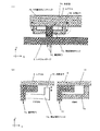
以上、従来の露光装置は、レチクル101をレチクルクランプ103にクランプする際に、レチクルクランプ103には、図14に示す様に、レチクルクランプパッド103Aが構成され、レチクルクランプパッド103Aをバキュームパッドにすることにより、レチクル101を、真空吸引クランプする。 As described above, in the conventional exposure apparatus, when the reticle 101 is clamped to the reticle clamp 103, the reticle clamp 103 is configured with the reticle clamp pad 103A as shown in FIG. 14, and the reticle clamp pad 103A is used as a vacuum pad. Thus, the reticle 101 is clamped by vacuum suction.
その際、図14(2)に示すように、レチクルクランプパッド103Aの上面クランプ面に、異物103Bが付着した場合、レチクル面上のパターンをウエハ上に投影する際に、パターン面内デフォーカスの悪化及びウエハ上パターン精度の悪化が発生するという問題があった。また、レチクル101の面と4箇所のレチクルクランプパッド103Aの構成する面との間の平坦度差から、レチクル101の面をクランプ時に変形させ歪ませることがあった。
本発明では、上記従来例に示す様に、レチクル面とレチクルクランプ面との間の平坦度差から、レチクルクランプ時のレチクルへの歪みの発生を防ぐことが課題である。 In the present invention, as shown in the above conventional example, it is a problem to prevent the reticle from being distorted during reticle clamping from the difference in flatness between the reticle surface and the reticle clamping surface.
また、同じくクランプ面に付着した異物によるレチクルへの歪みの発生を抑えることが課題である。 Another problem is to suppress the occurrence of distortion on the reticle due to foreign matter adhering to the clamp surface.
本発明は、原版保持部への異物付着及び原版面と原版保持面間の平坦度の差による原版面の歪の発生を防ぎ、原版を歪ませることなく露光することが可能な露光装置を提供することを目的とする。 The present invention provides an exposure apparatus capable of preventing exposure of a master plate without distorting the master plate by preventing foreign matter from adhering to the master holder and distortion of the master plate due to the difference in flatness between the master surface and the master holding surface. The purpose is to do.
上記目的を達成するために、本発明は、原版ステージ上に保持された原版のパターンを、投影光学系を介して基板に投影転写する露光装置において、前記原版ステージに設けられ、第1の当接面を有し前記原版を保持する第1の保持手段と、前記原版ステージに設けられ、第2の当接面を有し前記原版を保持する第2の保持手段と、前記第1の当接面と前記第2の当接面の間に形成される溝に設けられ、第3の当接面を有し前記原版を保持する複数のピンと、前記溝を介して前記原版を吸引する吸引手段と、を備え、前記第2及び第3の当接面は、前記第1の当接面に対して変位可能で、前記第2及び第3の当接面は、前記原版ステージ上で前記第1の当接面に接触した前記原版に、変位して接触することを特徴とする。 In order to achieve the above object, the present invention provides an exposure apparatus for projecting and transferring an original pattern held on an original stage onto a substrate via a projection optical system. a first holding means for holding the original has a contact surface, provided on the original stage, a second holding means for holding the original has a second abutment surface, the first person A plurality of pins provided in a groove formed between a contact surface and the second contact surface, having a third contact surface and holding the original plate, and suction for sucking the original plate through the groove And the second and third contact surfaces are displaceable with respect to the first contact surface, and the second and third contact surfaces are arranged on the original stage. It is characterized by being displaced and in contact with the original plate in contact with the first contact surface.
また、本発明は、前記第2の原版保持手段が弾性を有する部材を含んで構成されていてもよく、前記第1の原版保持手段及び前記第2の原版保持手段の少なくともいずれか一方に、該原版に対して吸引保持する吸引保持手段を備えることができ、吸引保持手段としては真空吸引あるいは静電吸引のいずれを用いてもよい。 In the present invention, the second original holding means may include an elastic member, and at least one of the first original holding means and the second original holding means , raw version sucking and holding means for sucking and holding can Rukoto provided with respect to, it may be any of vacuum suction or electrostatic suction as the suction holding means.
また、前記第1の原版保持手段と前記第2の原版保持手段は、該原版を保持する際に、該第1及び第2の原版保持手段の該原版保持面が該原版に当接することが好ましく、前記第1の原版保持手段と前記第2の原版保持手段間に、吸引時に相互に当接する接合シール部位を設けることが好ましく、前記第2の原版保持手段は、前記保持面に垂直な方向において移動及び変形の少なくともいずれかが可能に支持されることが好ましく、前記当接シール部位はテーパ構造の一部であることが好ましい。 Further, when the first original holding means and the second original holding means hold the original, the original holding surfaces of the first and second original holding means may come into contact with the original. preferably, between the said first original holding means second original holding means, it is preferable to provide a bonding seal portions abut against each other at the time of suction, the second original plate holding means is vertical to the holding surface it is preferred that at least one of Oite moved and deformed in the direction Ru is movably supported such, the contact seal portion is a portion der Rukoto tapered structure is preferred.
また、本発明は、上記いずれかの露光装置を用いてデバイスを製造する工程を有するデバイス製造方法にも適用可能である。 The present invention can also be applied to a device manufacturing method having a step of manufacturing a device using any of the above exposure apparatuses.
本発明では、原版面と原版保持面の間の平坦度差が生じた際や、原版面と原版保持面の間に異物が付着した際に、保持面を位置決めする第1の原版保持部材と、保持面に対して吸引力を発生させながら異物や原版面の状態に対して、弾性変形しながら沿わすことにより吸引クランプする第2の原版保持面を分離して設けることにより、異物及び原版面と原版保持面間の平坦度の差による原版面の歪の発生を防ぐ。 In the present invention, the first original holding member for positioning the holding surface when a flatness difference occurs between the original surface and the original holding surface or when foreign matter adheres between the original surface and the original holding surface; The second original holding surface that is clamped by suction while being elastically deformed with respect to the state of the foreign matter or the original plate surface while generating a suction force on the holding surface is provided separately. Prevents the distortion of the original plate due to the difference in flatness between the plate and the original holding surface.
本発明では、原版保持部への異物付着及び原版面と原版保持面間の平坦度の差による原版面の歪の発生を防ぎ、原版を歪ませることなく露光可能な露光装置を提供することができるという効果がある。 In the present invention, it is possible to provide an exposure apparatus capable of preventing exposure of foreign material to the original plate holding portion and preventing generation of distortion of the original plate surface due to a difference in flatness between the original plate surface and the original plate holding surface, without distorting the original plate. There is an effect that can be done.
本発明を実施するための最良の形態として、原版がレチクルであり、基板がウエハである場合の実施例について、以下に図面を参照しながら詳細に説明する。 As the best mode for carrying out the present invention, an embodiment in which the original plate is a reticle and the substrate is a wafer will be described in detail with reference to the drawings.
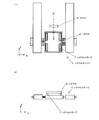
図1は本発明の実施例1に係る露光装置を概念的に示す側面図、図2は本発明の実施例1に係るレチクルステージを概念的に示す斜視図、図3は図1の露光装置の要部を示す側面図、図4は図1の要部を示し、(1)が平面図、(2)が側面図である。
1 is a side view conceptually showing an exposure apparatus according to
ここで、1は照明系ユニットであり、露光光を光源から導出し、成形均一な露光光とする。2はレチクルステージであり、露光原版(レチクル)を搭載し、露光光に対して原版(レチクル)をスキャン露光させる。3は縮小投影レンズであり、原版(レチクル)上のパターンを、シリコン基板より成るウエハ上に縮小投影する。4はウエハステージであり、シリコン基板であるウエハを搭載し、レチクルステージ2と同期して、露光光に対してスキャン移動露光する。
Here,
5は露光装置本体であり、レチクルステージ2、縮小投影レンズ3、及びウエハステージ4等を支持する。6は、原版としてのレチクルであり、投影パターンが形成されている。7はレチクルクランプであり、レチクルステージ2上に構成され、レチクル6を吸着保持位置決めする。8はスリット部材であり、レチクル6の原版パターンに対してスリット状の露光光を透過させる。
An exposure apparatus body 5 supports the
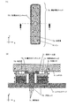
上記露光装置は、図5に示ように、レチクル6を、レチクルステージ2上のレチクルクランプ7に位置決め保持する構成を有する。そして、図5(1)は、レチクルクランプ7の上面に、レチクル6がクランプ位置決め保持されている状態を示し、図5(2)はクランプ状態を示す断面図である。
As shown in FIG. 5, the exposure apparatus has a configuration in which the
ここで、レチクルクランプ7は、レチクル6をZ方向で位置決めする、Z位置決めピンチャック7Bが設けられ、第1の当接面であるレチクル6との当接面には真空吸引する真空吸引手段7Cが配管され、吸引固定保持する。
Here, the reticle clamp 7 is provided with a Z
さらに、Z位置決めピンチャック7Bの周辺部に、Z位置決めピンチャック7Bに対して弾性変位可能に支持された薄板弾性チャック7Aが配置される。
Further, a thin plate
薄板弾性チャック7Aの実装状態を、図6に示す。薄板弾性チャック7Aには、吸着溝7Dが設けられ、真空吸引手段7Cにより真空室を形成する。さらに、薄板弾性チャック7Aの周辺外周部には、第2の当接面である外周土手7Eが設けられ、レチクル6に対して当接する面となる。また、吸着溝7Dの一部には、図6(1)及び(3)に示すように、複数のピン7Fが設けられ、第3の当接面である先端部がレチクル6に当接するように構成されている。
The mounting state of the thin
以上の構成で、レチクル6をクランプする際の、レチクルクランプ7の実施例機能説明図を、図7に記す。図7(1)は断面図であり、図7(2)は、その二点鎖線の楕円内の拡大断面図であって、レチクル6に対する、薄板弾性チャック7Aのクランプ時の変位状態を示す。ここで、レチクル6は、Z位置決めピンチャック7Bに対して、Z及びXY面内の位置決め後に搭載される。さらに、初期状態であるレチクル6への薄板弾性チャック7Aの非吸着時(図7(2)の左側図)には、薄板弾性チャック7Aは、レチクル6に対して、外周土手7Eが非接触状態で退避位置に位置する。
FIG. 7 is a functional explanatory diagram of the embodiment of the reticle clamp 7 when the
さらに、真空吸引手段7Cにより吸引固定される状態では、吸着時(図7(2)の右側図)に示す様に、薄板弾性チャック7Aの外周土手7Eは、弾性変位してレチクル6に当接し、レチクル6に対して、吸着溝7Dの真空吸着面により真空吸着保持力を発生させる。
Further, in the state of being sucked and fixed by the vacuum suction means 7C, the outer
この際、レチクル6の辺に倣う状態で、薄板弾性チャック7Aが当接することにより、レチクル6へのクランプ時の歪の発生を抑える効果がある。また同時に、図6(3)に示すように、吸着溝7Dの複数部位に、ピン7Fを設けることにより、レチクル6との当接面への異物の付着確率を低減し、異物の付着に起因する歪の発生を抑えることも可能になる。
At this time, the thin plate
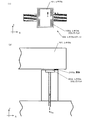
本発明の実施例2を、図8に示す。実施例1では、薄板弾性チャック7Aは、Z位置決めピンチャック7Bに固定あるいは一体構造で、弾性変位可能に支持されていたが、この実施例2では、薄板弾性チャック7Aは、Z位置決めピンチャック7Bに対し、完全に分離支持されることも可能である。
A second embodiment of the present invention is shown in FIG. In the first embodiment, the thin plate
薄板弾性チャック7Aは、板バネ7Gで分離弾性支持することにより、Z位置決めピンチャック7Bに対して自由にZ移動可能になる。板バネ7G自身は、レチクルステージ2上の板バネベース7Hに固定されている。
The thin plate
上記構成で、図9に、薄板弾性チャック7Aの弾性移動状態を示す。図9(1)に示すように、薄板弾性チャック7Aは、板バネ7GによりZ方向にのみ自由に弾性支持されている。ここで、レチクル6は、Z位置決めピンチャック7Bに対して、Z及びXY面内の位置決め後に搭載される。さらに、初期状態であるレチクル6への薄板弾性チャック7Aの非吸着時には、図9(2)の左側図に示すように、薄板弾性チャック7Aは、レチクル6に対して、外周土手7Eが非接触状態で退避位置に位置する。
FIG. 9 shows an elastic movement state of the thin plate
さらに、真空吸引手段7Cにより吸引固定される状態では、吸着時(図9(2)の右側図参照)に示す様に、薄板弾性チャック7Aは、外周土手7Eが、レチクル6に弾性変位して当接し、かつ、当接シール面7Jが、Z位置決めピンチャック7Bに当接することにより、レチクル6に対して、吸着溝7D(図8参照)の真空吸着面により真空吸着保持力を発生させる。
Further, in the state of being sucked and fixed by the vacuum suction means 7C, as shown at the time of suction (see the right side of FIG. 9 (2)), the thin plate
この際、レチクル6の辺に倣う状態で、薄板弾性チャック7Aがレチクル6に当接することにより、レチクル6へのクランプ時の歪の発生を抑える効果がある。
At this time, the thin plate
また同時に、図8(1)に示すように、吸着溝7Dの複数部位に、図6(3)に示すのと同様に該溝の底から上向きに突出し上端がレチクル6の裏面に当接するピン7Fを設けることにより、レチクル6との当接面への異物の付着確率を低減し、異物の付着に起因する歪の発生を抑えることも可能になる。
At the same time, as shown in FIG. 8 (1), a pin that protrudes upward from the bottom of the groove and has an upper end abutting against the back surface of the
本発明の実施例3に係る露光装置を、図10に示す。実施例2では、薄板状板バネにより弾性支持しているが、この実施例3では、Z方向に弾性変位可能な折り曲げ構造の弾性ヒンジ7Kを用いる構成も可能である。 FIG. 10 shows an exposure apparatus according to Example 3 of the present invention. In the second embodiment, it is elastically supported by a thin plate spring. However, in the third embodiment, a configuration using an elastic hinge 7K having a bending structure capable of elastic displacement in the Z direction is also possible.
薄板弾性チャック7Aは、弾性ヒンジ7Kで分離弾性支持することにより、Z位置決めピンチャック7Bに対して自由にZ移動可能になる。弾性ヒンジ7K自身は、レチクルステージ2上に固定されている。
The thin plate
上記構成で、図9を用いて、薄板弾性チャック7Aの弾性移動状態について説明する。図9(1)に示すように、薄板弾性チャック7Aは、弾性ヒンジ7KによりZ方向にのみ自由に弾性支持されている。ここで、レチクル6は、Z位置決めピンチャック7Bに対して、Z及びXY面内の位置決め後に搭載される。さらに、初期状態であるレチクル6への薄板弾性チャック7Aの非吸着時には、図9(2)に示すように、薄板弾性チャック7Aは、レチクル6に対して、外周土手7Eが非接触状態で退避位置に位置する。
The elastic movement state of the thin plate
さらに、真空吸引手段7Cにより吸引固定される状態では、図9(3)の吸着時に示す様に、薄板弾性チャック7Aの外周土手7Eが、レチクル6に弾性変位して当接し、かつ、当接シール面7Jが、Z位置決めピンチャック7Bに当接することにより、レチクル6に対して、吸着溝7Dの真空吸着面により真空吸着保持力を発生させる。
Further, in the state of being sucked and fixed by the vacuum suction means 7C, the outer
この際、レチクル6の辺に倣う状態で、薄板弾性チャック7Aが当接することにより、レチクル6へのクランプ時の歪の発生を抑える効果がある。また同時に、図10(1)に示すように、吸着溝7Dの複数部位に、図6(3)に示すのと同様に該溝の底から上向きに突出し上端がレチクル6の裏面に当接するピン7Fを設けることにより、レチクル6との当接面への異物の付着確率を低減し、異物の付着に起因する歪の発生を抑えることも可能になる。
At this time, the thin plate
本発明の実施例4を、図11に示す。Z位置決めピンチャック7Bと、薄板弾性チャック7A間の当接シール面を、図11(2)に示す様に、テーパ構造の当接シール面7Lにすることにより、レチクルクランプ7は、真空吸引時に当接面7Lがセルフセンタリングする効果により、安定的にシールすることが可能になる。
A fourth embodiment of the present invention is shown in FIG. When the contact sealing surface between the Z
次に、本発明の実施例5として、実施例1〜4のいずれかの露光装置を利用した半導体デバイスの製造プロセスを説明する。図15は半導体デバイスの全体的な製造プロセスのフローを示す図である。ステップ1(回路設計)では半導体デバイスの回路設計を行う。ステップ2(マスク作製)では設計した回路パターンに基づいてマスクを作製する。 Next, as a fifth embodiment of the present invention, a semiconductor device manufacturing process using any one of the exposure apparatuses according to the first to fourth embodiments will be described. FIG. 15 is a diagram showing a flow of an entire manufacturing process of a semiconductor device. In step 1 (circuit design), a semiconductor device circuit is designed. In step 2 (mask fabrication), a mask is fabricated based on the designed circuit pattern.
一方、ステップ3(ウエハ製造)ではシリコン等の材料を用いてウエハを製造する。ステップ4(ウエハプロセス)は前工程と呼ばれ、上記のマスクとウエハを用いて、上記の露光装置によりリソグラフィ技術を利用してウエハ上に実際の回路を形成する。次のステップ5(組み立て)は後工程と呼ばれ、ステップ5によって作製されたウエハを用いて半導体チップ化する工程であり、アッセンブリ工程(ダイシング、ボンディング)、パッケージング工程(チップ封入)等の組み立て工程を含む。ステップ6(検査)ではステップ5で作製された半導体デバイスの動作確認テスト、耐久性テスト等の検査を行う。こうした工程を経て半導体デバイスが完成し、ステップ7でこれを出荷する。 On the other hand, in step 3 (wafer manufacture), a wafer is manufactured using a material such as silicon. Step 4 (wafer process) is called a pre-process, and an actual circuit is formed on the wafer by using the above-described exposure apparatus and lithography technology using the above-described mask and wafer. The next step 5 (assembly) is called a post-process, which is a process for forming a semiconductor chip using the wafer produced in step 5, and is an assembly process (dicing, bonding), packaging process (chip encapsulation), etc. Process. In step 6 (inspection), the semiconductor device manufactured in step 5 undergoes inspections such as an operation confirmation test and a durability test. A semiconductor device is completed through these processes, and is shipped in Step 7.
上記ステップ4のウエハプロセスは以下のステップを有する。ウエハの表面を酸化させる酸化ステップ、ウエハ表面に絶縁膜を成膜するCVDステップ、ウエハ上に電極を蒸着によって形成する電極形成ステップ、ウエハにイオンを打ち込むイオン打ち込みステップ、ウエハに感光剤を塗布するレジスト処理ステップ、上記の露光装置によって回路パターンをレジスト処理ステップ後のウエハに転写する露光ステップ、露光ステップで露光したウエハを現像する現像ステップ、現像ステップで現像したレジスト像以外の部分を削り取るエッチングステップ、エッチングが済んで不要となったレジストを取り除くレジスト剥離ステップ。これらのステップを繰り返し行うことによって、ウエハ上に多重に回路パターンを形成する。 The wafer process in step 4 includes the following steps. An oxidation step for oxidizing the surface of the wafer, a CVD step for forming an insulating film on the wafer surface, an electrode formation step for forming electrodes on the wafer by vapor deposition, an ion implantation step for implanting ions on the wafer, and applying a photosensitive agent to the wafer A resist processing step, an exposure step for transferring the circuit pattern to the wafer after the resist processing step by the above exposure apparatus, a development step for developing the wafer exposed in the exposure step, and an etching step for scraping off portions other than the resist image developed in the development step A resist stripping step that removes the resist that has become unnecessary after etching. By repeating these steps, multiple circuit patterns are formed on the wafer.
1:照明系ユニット、2:レチクルステージ、3:縮小投影レンズ、4:ウエハステージ、4A:ウエハ、5:露光装置本体、6:レチクル、7:レチクルクランプ、7A:薄板弾性チャック、7B:Z位置決めピンチャック、7C:真空吸引手段、7D:吸着溝、7E:外周土手、7F:ピン、7G:板バネ、7H:板バネベース、7J:当接シール面、7K:弾性ヒンジ、7L:当接シール面、8:スリット部材、101:レチクル、101A:スリット露光光、102:レチクルステージ、103:レチクルクランプ、103A:レチクルクランプパッド、103B:異物、104:縮小投影レンズ、105:ウエハ、106:ウエハステージ。 1: illumination system unit, 2: reticle stage, 3: reduction projection lens, 4: wafer stage, 4A: wafer, 5: exposure apparatus body, 6: reticle, 7: reticle clamp, 7A: thin plate elastic chuck, 7B: Z Positioning pin chuck, 7C: vacuum suction means, 7D: suction groove, 7E: outer periphery bank, 7F: pin, 7G: leaf spring, 7H: leaf spring base, 7J: contact seal surface, 7K: elastic hinge, 7L: contact Seal surface, 8: slit member, 101: reticle, 101A: slit exposure light, 102: reticle stage, 103: reticle clamp, 103A: reticle clamp pad, 103B: foreign matter, 104: reduction projection lens, 105: wafer, 106: Wafer stage.
Claims (10)
前記原版ステージに設けられ、第1の当接面を有し前記原版を保持する第1の保持手段と、
前記原版ステージに設けられ、第2の当接面を有し前記原版を保持する第2の保持手段と、
前記第1の当接面と前記第2の当接面の間に形成される溝に設けられ、第3の当接面を有し前記原版を保持する複数のピンと、
前記溝を介して前記原版を吸引する吸引手段と、を備え、
前記第2及び第3の当接面は、前記第1の当接面に対して変位可能で、
前記第2及び第3の当接面は、前記原版ステージ上で前記第1の当接面に接触した前記原版に、変位して接触することを特徴とする露光装置。 In an exposure apparatus that projects and transfers an original pattern held on an original stage onto a substrate via a projection optical system,
A first holding means provided on the original stage and having a first abutment surface for holding the original;
A second holding means provided on the original stage and having a second abutting surface to hold the original;
A plurality of pins provided in a groove formed between the first contact surface and the second contact surface, having a third contact surface and holding the original;
A suction means for sucking the original plate through the groove ,
The second and third contact surfaces are displaceable relative to the first contact surface;
The exposure apparatus according to claim 1, wherein the second and third contact surfaces are displaced in contact with the original plate in contact with the first contact surface on the original stage.
前記第1の保持手段と前記第2保持手段が当接する部位がテーパ構造であることを特徴とする請求項1または2に記載の露光装置。 The second holding means is supported separately from the first holding means, and when the second contact surface is displaced to contact the original plate, the first holding means and the second holding means are supported. The holding means is configured to contact,
3. The exposure apparatus according to claim 1, wherein a portion where the first holding unit and the second holding unit are in contact has a tapered structure .
前記原版に当接する第1保持面を有し、前記原版を前記投影光学系の光軸方向に位置決めする第1保持手段と、A first holding means that has a first holding surface in contact with the original, and positions the original in the optical axis direction of the projection optical system;
前記原版に当接する第2保持面と、吸着溝と、該吸着溝の内部に形成され前記第2保持面とは異なる位置で前記原版に当接するピンとを有する第2保持手段と、A second holding means having a second holding surface that comes into contact with the original, a suction groove, and a pin that is formed inside the suction groove and comes into contact with the original at a position different from the second holding surface;
前記吸着溝の内部の空間を排気する真空吸引手段とを備え、Vacuum suction means for exhausting the space inside the suction groove,
前記第2保持面および前記ピンが前記第1保持面に対して、前記光軸方向に変位可能に構成されることを特徴とする露光装置。An exposure apparatus, wherein the second holding surface and the pin are configured to be displaceable in the optical axis direction with respect to the first holding surface.
前記吸引手段の吸引にともない前記第2保持手段が弾性変形することによって、前記第2の保持面および前記ピンが変位して前記原版に当接することを特徴とする請求項8または9に記載の露光装置。The said 2nd holding surface and the said pin are displaced by the said 2nd holding means elastically deforming with the suction of the said suction means, and contact | abut to the said negative | original plate, It is characterized by the above-mentioned. Exposure device.
Priority Applications (2)
| Application Number | Priority Date | Filing Date | Title |
|---|---|---|---|
| JP2004040977A JP4411100B2 (en) | 2004-02-18 | 2004-02-18 | Exposure equipment |
| US11/059,331 US7307698B2 (en) | 2004-02-18 | 2005-02-17 | Exposure apparatus and device manufacturing method |
Applications Claiming Priority (1)
| Application Number | Priority Date | Filing Date | Title |
|---|---|---|---|
| JP2004040977A JP4411100B2 (en) | 2004-02-18 | 2004-02-18 | Exposure equipment |
Publications (3)
| Publication Number | Publication Date |
|---|---|
| JP2005235890A JP2005235890A (en) | 2005-09-02 |
| JP2005235890A5 JP2005235890A5 (en) | 2008-11-20 |
| JP4411100B2 true JP4411100B2 (en) | 2010-02-10 |
Family
ID=34857908
Family Applications (1)
| Application Number | Title | Priority Date | Filing Date |
|---|---|---|---|
| JP2004040977A Expired - Fee Related JP4411100B2 (en) | 2004-02-18 | 2004-02-18 | Exposure equipment |
Country Status (2)
| Country | Link |
|---|---|
| US (1) | US7307698B2 (en) |
| JP (1) | JP4411100B2 (en) |
Families Citing this family (14)
| Publication number | Priority date | Publication date | Assignee | Title |
|---|---|---|---|---|
| JP4666908B2 (en) | 2003-12-12 | 2011-04-06 | キヤノン株式会社 | Exposure apparatus, measurement method, and device manufacturing method |
| JP2006120798A (en) * | 2004-10-20 | 2006-05-11 | Canon Inc | Exposure apparatus |
| JP2006261156A (en) * | 2005-03-15 | 2006-09-28 | Canon Inc | Apparatus for holding original plate and exposure apparatus using the same |
| US7352438B2 (en) * | 2006-02-14 | 2008-04-01 | Asml Netherlands B.V. | Lithographic apparatus and device manufacturing method |
| US20070268476A1 (en) * | 2006-05-19 | 2007-11-22 | Nikon Corporation | Kinematic chucks for reticles and other planar bodies |
| JPWO2007135998A1 (en) * | 2006-05-24 | 2009-10-01 | 株式会社ニコン | Holding apparatus and exposure apparatus |
| US7869003B2 (en) * | 2006-07-12 | 2011-01-11 | Asml Holding Nv | Lithographic apparatus and device manufacturing method with reticle gripper |
| JP5013941B2 (en) * | 2007-04-19 | 2012-08-29 | キヤノン株式会社 | Stage apparatus, exposure apparatus, and device manufacturing method |
| JP2011023425A (en) | 2009-07-13 | 2011-02-03 | Canon Inc | Stage apparatus, exposure apparatus, and method of manufacturing device |
| DE102009037939A1 (en) * | 2009-08-19 | 2011-06-30 | ERS electronic GmbH, 82110 | Method and device for determining the deflection of a disk-shaped workpiece |
| NL2006190A (en) * | 2010-03-11 | 2011-09-13 | Asml Netherlands Bv | Lithographic apparatus and device manufacturing method. |
| US20130250271A1 (en) * | 2012-02-17 | 2013-09-26 | Nikon Corporation | Stage assembly with secure device holder |
| NL2020281A (en) | 2017-02-10 | 2018-08-22 | Asml Holding Nv | Reticle clamping device |
| US11353800B2 (en) * | 2017-12-28 | 2022-06-07 | Onto Innovation Inc. | Conformal stage |
Family Cites Families (16)
| Publication number | Priority date | Publication date | Assignee | Title |
|---|---|---|---|---|
| JPS62100753A (en) * | 1985-10-29 | 1987-05-11 | Canon Inc | Multi-point supporting reticle chuck |
| JP2750554B2 (en) * | 1992-03-31 | 1998-05-13 | 日本電信電話株式会社 | Vacuum suction device |
| JPH07136885A (en) * | 1993-06-30 | 1995-05-30 | Toshiba Corp | Vacuum chuck |
| JPH07326566A (en) | 1994-05-31 | 1995-12-12 | Nikon Corp | Mask support pedestal |
| JP3372127B2 (en) * | 1994-11-18 | 2003-01-27 | 日本電信電話株式会社 | Vacuum suction device |
| JPH08167553A (en) | 1994-12-14 | 1996-06-25 | Toshiba Mach Co Ltd | Work fixing device |
| JP3708984B2 (en) | 1995-04-17 | 2005-10-19 | 東芝機械株式会社 | Fixing device for workpiece |
| JP3483452B2 (en) * | 1998-02-04 | 2004-01-06 | キヤノン株式会社 | Stage apparatus, exposure apparatus, and device manufacturing method |
| JP3810039B2 (en) * | 1998-05-06 | 2006-08-16 | キヤノン株式会社 | Stage equipment |
| US6196532B1 (en) * | 1999-08-27 | 2001-03-06 | Applied Materials, Inc. | 3 point vacuum chuck with non-resilient support members |
| JP2001332480A (en) * | 2000-05-24 | 2001-11-30 | Canon Inc | Original chuck, aligner with original chuck, and semiconductor device-manufacturing method |
| WO2002065519A1 (en) * | 2001-02-13 | 2002-08-22 | Nikon Corporation | Holding device, holding method, exposure device, and device manufacturing method |
| US6801301B2 (en) * | 2001-10-12 | 2004-10-05 | Canon Kabushiki Kaisha | Exposure apparatus |
| TW200303593A (en) * | 2002-02-19 | 2003-09-01 | Olympus Optical Co | Substrate sucking apparatus |
| JP3826118B2 (en) * | 2003-07-08 | 2006-09-27 | キヤノン株式会社 | Exposure equipment |
| US7119884B2 (en) * | 2003-12-24 | 2006-10-10 | Asml Netherlands B.V. | Lithographic apparatus and device manufacturing method |
-
2004
- 2004-02-18 JP JP2004040977A patent/JP4411100B2/en not_active Expired - Fee Related
-
2005
- 2005-02-17 US US11/059,331 patent/US7307698B2/en active Active
Also Published As
| Publication number | Publication date |
|---|---|
| JP2005235890A (en) | 2005-09-02 |
| US20050185166A1 (en) | 2005-08-25 |
| US7307698B2 (en) | 2007-12-11 |
Similar Documents
| Publication | Publication Date | Title |
|---|---|---|
| US7307698B2 (en) | Exposure apparatus and device manufacturing method | |
| US20050122505A1 (en) | Substrate-holding technique | |
| JP2005150527A (en) | Holding device, exposure device and manufacturing method using the same | |
| JP2008103703A (en) | Substrate retaining unit, exposure apparatus provided with substrate retaining unit, and device manufacturing method | |
| JP4411158B2 (en) | Exposure equipment | |
| US5485495A (en) | X-ray mask, and exposure apparatus and device production using the mask | |
| KR20080026499A (en) | Substrate-retaining unit | |
| JP2020112695A (en) | Exposure apparatus, exposure method and method for manufacturing article | |
| US20090044837A1 (en) | Substrate processing apparatus | |
| JP2001127145A (en) | Method and device for holding substrate with suction and exposing device and device manufacturing method using the device | |
| JP2004140071A (en) | Substrate holding device | |
| JP2001185607A (en) | Substrate suction holding device and device manufacturing method | |
| JP2005093654A (en) | Stage device, aligner using the same, and device manufacturing method using aligner | |
| JP2001144168A (en) | Electrostatic chuck, charged particle beam exposure system having the same, and wafer holding method and device manufacturing method using the chuck | |
| JP2003051535A (en) | Wafer holder, aligner and device production method | |
| JP4332409B2 (en) | Substrate holding mechanism, exposure apparatus using the same, and device manufacturing method | |
| JP2005228978A (en) | Exposure device and manufacturing method for semiconductor device | |
| US6309212B1 (en) | Substrate conveying system and device manufacturing method using the same | |
| TW202236496A (en) | Chuck, substrate holding apparatus, substrate processing apparatus, and method of manufacturing article capable of reducing the twisting of a substrate by setting the heights of the convex portions on the inner peripheral side and the convex portions on the outer peripheral side into a predetermined relationship | |
| JP2022134074A (en) | Chuck, substrate-holding device, substrate-processing device, and production method of article | |
| JP2009016388A (en) | Original transfer device, exposure device, and method for manufacturing device | |
| JP2007207996A (en) | Substrate holding device | |
| JP2006261156A (en) | Apparatus for holding original plate and exposure apparatus using the same | |
| JP2004165439A (en) | Stage equipment | |
| JP3200265B2 (en) | Mask holding method and mask, and device manufacturing method using the same |
Legal Events
| Date | Code | Title | Description |
|---|---|---|---|
| A521 | Request for written amendment filed |
Free format text: JAPANESE INTERMEDIATE CODE: A523 Effective date: 20070219 |
|
| A621 | Written request for application examination |
Free format text: JAPANESE INTERMEDIATE CODE: A621 Effective date: 20070219 |
|
| A977 | Report on retrieval |
Free format text: JAPANESE INTERMEDIATE CODE: A971007 Effective date: 20080715 |
|
| A521 | Request for written amendment filed |
Free format text: JAPANESE INTERMEDIATE CODE: A523 Effective date: 20081003 |
|
| RD02 | Notification of acceptance of power of attorney |
Free format text: JAPANESE INTERMEDIATE CODE: A7422 Effective date: 20081003 |
|
| RD01 | Notification of change of attorney |
Free format text: JAPANESE INTERMEDIATE CODE: A7421 Effective date: 20090406 |
|
| A131 | Notification of reasons for refusal |
Free format text: JAPANESE INTERMEDIATE CODE: A131 Effective date: 20090519 |
|
| A521 | Request for written amendment filed |
Free format text: JAPANESE INTERMEDIATE CODE: A523 Effective date: 20090717 |
|
| TRDD | Decision of grant or rejection written | ||
| A01 | Written decision to grant a patent or to grant a registration (utility model) |
Free format text: JAPANESE INTERMEDIATE CODE: A01 Effective date: 20091110 |
|
| A01 | Written decision to grant a patent or to grant a registration (utility model) |
Free format text: JAPANESE INTERMEDIATE CODE: A01 |
|
| A61 | First payment of annual fees (during grant procedure) |
Free format text: JAPANESE INTERMEDIATE CODE: A61 Effective date: 20091116 |
|
| R150 | Certificate of patent or registration of utility model |
Ref document number: 4411100 Country of ref document: JP Free format text: JAPANESE INTERMEDIATE CODE: R150 Free format text: JAPANESE INTERMEDIATE CODE: R150 |
|
| FPAY | Renewal fee payment (event date is renewal date of database) |
Free format text: PAYMENT UNTIL: 20121120 Year of fee payment: 3 |
|
| FPAY | Renewal fee payment (event date is renewal date of database) |
Free format text: PAYMENT UNTIL: 20131120 Year of fee payment: 4 |
|
| LAPS | Cancellation because of no payment of annual fees |