JP4408571B2 - Electronic commutation motor - Google Patents
Electronic commutation motor Download PDFInfo
- Publication number
- JP4408571B2 JP4408571B2 JP2000581736A JP2000581736A JP4408571B2 JP 4408571 B2 JP4408571 B2 JP 4408571B2 JP 2000581736 A JP2000581736 A JP 2000581736A JP 2000581736 A JP2000581736 A JP 2000581736A JP 4408571 B2 JP4408571 B2 JP 4408571B2
- Authority
- JP
- Japan
- Prior art keywords
- motor
- transistor
- microprocessor
- current
- commutation
- Prior art date
- Legal status (The legal status is an assumption and is not a legal conclusion. Google has not performed a legal analysis and makes no representation as to the accuracy of the status listed.)
- Expired - Fee Related
Links
Images


Classifications
-
- H—ELECTRICITY
- H02—GENERATION; CONVERSION OR DISTRIBUTION OF ELECTRIC POWER
- H02P—CONTROL OR REGULATION OF ELECTRIC MOTORS, ELECTRIC GENERATORS OR DYNAMO-ELECTRIC CONVERTERS; CONTROLLING TRANSFORMERS, REACTORS OR CHOKE COILS
- H02P6/00—Arrangements for controlling synchronous motors or other dynamo-electric motors using electronic commutation dependent on the rotor position; Electronic commutators therefor
- H02P6/24—Arrangements for stopping
-
- H—ELECTRICITY
- H02—GENERATION; CONVERSION OR DISTRIBUTION OF ELECTRIC POWER
- H02P—CONTROL OR REGULATION OF ELECTRIC MOTORS, ELECTRIC GENERATORS OR DYNAMO-ELECTRIC CONVERTERS; CONTROLLING TRANSFORMERS, REACTORS OR CHOKE COILS
- H02P6/00—Arrangements for controlling synchronous motors or other dynamo-electric motors using electronic commutation dependent on the rotor position; Electronic commutators therefor
- H02P6/14—Electronic commutators
- H02P6/16—Circuit arrangements for detecting position
-
- H—ELECTRICITY
- H02—GENERATION; CONVERSION OR DISTRIBUTION OF ELECTRIC POWER
- H02P—CONTROL OR REGULATION OF ELECTRIC MOTORS, ELECTRIC GENERATORS OR DYNAMO-ELECTRIC CONVERTERS; CONTROLLING TRANSFORMERS, REACTORS OR CHOKE COILS
- H02P6/00—Arrangements for controlling synchronous motors or other dynamo-electric motors using electronic commutation dependent on the rotor position; Electronic commutators therefor
- H02P6/28—Arrangements for controlling current
Landscapes
- Engineering & Computer Science (AREA)
- Power Engineering (AREA)
- Control Of Motors That Do Not Use Commutators (AREA)
- Control Of Direct Current Motors (AREA)
- Motor Or Generator Current Collectors (AREA)
- Dc Machiner (AREA)
Abstract
Description
【0001】
【技術分野】
本発明は、永久磁石ロータとステータとを有する電子コミュテーション式モータに関する。
【0002】
【技術的背景】
この種の電子コミュテーション式モータは多種多様に公知である。
【0003】
【発明が解決しようとする課題】
本発明の課題は、新規の電子コミュテーション式モータを提供することである。
【0004】
【解決手段】
本発明によればこの課題は、ロータとステータとを有する電子コミュテーション式モータであって、
固定子巻線装置と、コミュテーション装置とを有し、
前記固定子巻線装置には、フルブリッジ回路を介して電流が直流源から給電可能であり、
前記フルブリッジ回路は各ブリッジ分岐路に、1つの上側MOSFETトランジスタと1つの下側トランジスタとを有し、
前記上側MOSFETトランジスタは直流源の正の線路と接続されており、
前記下側トランジスタは直流源の負の線路と接続されており、
前記コミュテーション装置は、前記トランジスタをコミュテーションし、
かつ前記コミュテーション装置は、少なくともロータ位置に依存して第1のブリッジ分岐路では1つのトランジスタだけがスイッチオンされ、第2のブリッジ分岐路ではPWM信号によって制御されて、上側トランジスタおよび下側トランジスタが交互にスイッチオンされるように構成されており、
さらに、少なくとも1つのモータ量に依存して、所定の値を上回る制動電流がブリッジ回路に発生するとき、前記PWM信号のデューティ比を変化させて、モータにより発電的に形成される電流が低減されるように構成された装置が設けられている電子コミュテーション式モータにより解決される。
【0005】
この種の電子コミュテーション式モータは、外部の影響により所望の回転数を上回ることがあり得るような動作タスクに非常に適する。これによりこの形式のモータはブリッジ回路により制動動作へ自動的に移行し、この制動動作においては所定のモータ限界値を上回らない、または実質的に上回らないことが保証される。
【0006】
前記課題の別の解決手段は、ロータとステータとを備える電子コミュテーション式モータであって、
固定子巻線装置を有し、
該固定子巻線装置には、フルブリッジ回路を介して電流が直流源から給電され、
前記フルブリッジ回路は、各ブリッジ分岐路に1つの上側NMOSトランジスタと1つの下側トランジスタとを有し、
前記上側NMOSトランジスタは前記直流源の正の線路と接続されており、
前記下側トランジスタは前記直流源の負の線路と接続されており、
ブリッジ分岐路の上側トランジスタにはそれぞれ蓄積コンデンサが配属されており、
該蓄積コンデンサは前記ブリッジ分岐路の下側トランジスタを介して充電可能であり、かつ前記上側トランジスタに制御電圧を供給するために用いられ、
さらに前記トランジスタをコミュテーションするためのコミュテーション装置を有し、
該コミュテーション装置は、少なくともロータ位置に依存して、第1のブリッジ分岐路では1つのトランジスタだけがスイッチオンされ、第2のブリッジ分岐路では上側トランジスタと下側トランジスタとが交互にスイッチオンされるように構成されており、
モータ回転数が監視され、所定の回転数値を下回る際、所定の時間の経過後、フルブリッジ回路の上側トランジスタが短時間阻止され、該フルブリッジ回路の下側トランジスタが短時間スイッチオンされ、
これにより上側トランジスタの蓄積コンデンサが充電され、このことにより該上側トランジスタの確実な制御が、回転数が低い場合またはモータが静止状態にある場合でも保証される電子コミュテーション式モータにより得られる。
【0007】
従ってNMOSトランジスタによるこの種のフルブリッジ回路を有するモータにおいて、回転数が非常に低くなる場合、またはゼロに低下するような場合でも駆動能力が保証される。
【0008】
前記課題の解決手段は、永久磁石ロータと、ステータと、固定子巻線装置と、コミュテーション装置と、マイクロプロセッサまたはマイクロコントローラ、以下、マイクロプロセッサと称する、とを有する電子コミュテーション式モータの駆動方法であって、
前記固定子巻線装置には、フルブリッジ回路を介して電流が直流源から給電可能であり、
前記フルブリッジ回路は複数のブリッジ分岐路を有し、各ブリッジ分岐路に1つの上側MOSFETトランジスタと1つの下側トランジスタとを有し、
前記上側MOSFETトランジスタは直流源の正の線路と接続されており、
前記下側トランジスタは直流源の負の線路と接続されており、
前記コミュテーション装置は前記トランジスタをコミュテーションし、
かつ前記コミュテーション装置は、少なくともロータ位置に依存して、第1のブリッジ分岐路では1つのトランジスタだけがスイッチオンされ、第2のブリッジ分岐路ではPWM信号により制御されて、上側トランジスタと下側トランジスタとが交互にスイッチオンされるように構成されている形式のモータの駆動方法において、
マイクロプロセッサにて、モータの合成的(synthetisch)モデルに基づき、該モータに供給される直流電圧がモータで誘導される電圧と所定の関係にあるか否かを監視し、
前記関係が維持されない場合、該関係を補正するためにPWM信号のデューティ比を相応に変化し、
該PWM信号により第2のブリッジ分岐路の上側トランジスタと下側トランジスタとが交互にスイッチオンされ、
前記デューティ比の変化によって、前記所定の関係の逸脱に対抗的に作用する、電子コミュテーション式モータの駆動方法によっても得られる。
【0009】
このようにしてソフトウエアを相応に構成することにより、すなわちモータの合成的(場合により単純化された)モデルにより、モータが過負荷により脅かされない領域で動作するようになる。例えば高い固有電力を有する多くのモータでは、過度に高い駆動電流または制動電流によってステータに強い磁界が形成され、永久磁石ロータが減磁されることがある。このことは本発明の方法により簡単に阻止され、これにより動作確実性が格段に向上する。
【0010】
前記課題の別の解決手段は、ロータとステータとを有する電子コミュテーション式モータであって、
前記ステータには固定子巻線装置が配置されており、
該固定子巻線装置には、並列に接続された複数のブリッジ分岐路を備えるフルブリッジ回路が配属されており、
前記ブリッジ分岐路の各々は1つの上側トランジスタと1つの下側トランジスタとを有し、
前記上側トランジスタは直流源の正の線路と接続されており、
前記下側トランジスタは直流源の負の線路と接続されており、
ブリッジ分岐路の前記2つのトランジスタにはそれぞれ1つの制御回路が配属されており、
該制御回路は、第1の入力信号に依存してアクティブまたは非アクティブにされ、かつ当該非アクティブ状態では配属されたブリッジ分岐路の2つのトランジスタを阻止し、
かつ前記制御回路は第2の入力信号に依存して、第1の入力信号によりアクティブ化された状態では、上側トランジスタまたは下側トランジスタのいずれかが導通制御されるように切替可能であり、
さらにマイクロプロセッサまたはマイクロコントローラ、以下マイクロプロセッサと称する、を有し、
該マイクロプロセッサは、第1の入力信号を第1の出力端に形成し、第2の入力信号を第2の出力端に形成し、
そして制御可能なデューティ比を備えるPWM信号の形態の第3の入力信号を有し、
該第3の入力信号は、制御回路に第2の入力信号とは並列にPWM信号源から供給可能であり、かつマイクロプロセッサの第2の出力端が所定のスイッチ状態に切り替えられるときだけ作用する電子コミュテーション式モータにより得られる。
【0011】
このことにより、PWM信号が制御回路の直前で初めて導入することに成功する。このことは回路を非常に簡単にするが、マイクロプロセッサはそれにもかかわらず制御回路を完全にコントロールする。これによりマイクロプロセッサは、PWM信号に依存せずに、配属されたブリッジ分岐路の上側トランジスタと下側トランジスタを制御することができる(例えばチャージポンプとして使用した場合)。しかし他方では、マイクロプロセッサの第2の出力を所定の回路状態に切り替えた後、このブリッジ分岐路をPWM信号により、例えばモータパラメータを調整するために制御することができる。
【0012】
本発明のさらなる詳細および有利な実施形態は、以下の説明および図面に示された実施例並びに従属請求項から明らかとなる。しかし実施例は本発明の限定として理解すべきものではない。従って、特許請求の範囲に付した図面参照符号(及び図番)も専ら発明の理解を助けるためのものに過ぎず、本発明を図示の態様に限定することを意図していない。ここに、本発明の好ましい実施の形態を示す:
(形態1) 本発明の第1の視点の、ロータとステータとを有する電子コミュテーション式モータは、
固定子巻線装置と、コミュテーション装置とを有し、
前記固定子巻線装置には、フルブリッジ回路を介して電流が直流源から給電可能であり、
前記フルブリッジ回路は各ブリッジ分岐路に、1つの上側MOSFETトランジスタと1つの下側トランジスタとを有し、
前記上側MOSFETトランジスタは直流源の正の線路と接続されており、
前記下側トランジスタは直流源の負の線路と接続されており、
前記コミュテーション装置は、前記トランジスタをコミュテーションし、かつ前記コミュテーション装置は、少なくともロータ位置に依存して第1のブリッジ分岐路では1つのトランジスタだけがスイッチオンされ、第2のブリッジ分岐路では上側トランジスタおよび下側トランジスタが交互にスイッチオンされるように構成され、
前記第2のブリッジ分岐路の前記上側トランジスタおよび前記下側トランジスタを所定のデューティ比で交互にスイッチオンするよう作動するPWM信号を生成するための発生器が設けられ、
さらに、少なくとも1つのモータ量に依存して、所定の値を上回る制動電流がフルブリッジ回路に発生するとき、前記PWM信号のデューティ比を変化させて、モータにより発電的に形成される電流が低減されるように構成された装置が設けられていることを特徴とする(第1基本構成)。
(形態2) 上記形態1の電子コミュテーション式モータにおいて、直流源における電圧を監視するための装置を有し、
該装置は、所定の上側限界値を前記電圧が上回るとき、フルブリッジ回路の全てのトランジスタを阻止することが好ましい。
(形態3) 上記形態2の電子コミュテーション式モータにおいて、モータ制御に用いるマイクロプロセッサまたはマイクロコントローラ(以下マイクロプロセッサと称する)を有し、
該マイクロプロセッサはA/D変換器を有し、
該A/D変換器は直流源の電圧をデジタル値に、マイクロプロセッサでのデジタル後続処理のために変換することが好ましい。
(形態4) 上記形態1〜3の何れかの電子コミュテーション式モータにおいて、モータ制御に用いるマイクロプロセッサまたはマイクロコントローラ(以下マイクロプロセッサと称する)を有し、
該マイクロプロセッサは動作時に、出力信号をフルブリッジ回路を制御するために送出し、
各ブリッジ分岐路にはコミュテーション構成素子が、当該ブリッジ分岐路の上側トランジスタと下側トランジスタとを交互にスイッチオンするために配属されており、
該コミュテーション構成素子は少なくとも2つの信号入力端を有し、
該信号入力端はマイクロプロセッサの別個の信号出力によって制御可能であり、
PWM信号が前記信号入力端の1つに供給可能であり、
該信号入力端に配属された、マイクロプロセッサの信号出力端は高抵抗状態に切替可能であり、
これにより前記マイクロプロセッサから、前記ブリッジ分岐路のトランジスタの交互スイッチオンがPWM信号によってアクティブにされることが好ましい。
(形態5) 上記形態1〜4の何れかの電子コミュテーション式モータにおいて、モータ制御に用いるマイクロプロセッサまたはマイクロコントローラ(以下マイクロプロセッサと称する)を有し、
該マイクロプロセッサはモータの回転数制御に用いられ、かつ少なくとも1つの出力端にプロセッサPWM信号をモータの回転数制御のために出力し、
さらに、前記プロセッサPWM信号のデューティ比を回転数に依存する値に制限するための装置を有することが好ましい。
(形態6) 上記形態5の電子コミュテーション式モータにおいて、前記デューティ比は制動過程時には、モータの回転数の減少と共に減少する最小値に制限されることが好ましい。
(形態7) 上記形態5又は6の電子コミュテーション式モータにおいて、プロセッサPWM信号は、そのデューティ比によって第1のコンデンサの充電状態を制御し、
第2のコンデンサが設けられており、
該第2のコンデンサは抵抗装置を介して前記第1のコンデンサと接続されており、
フルブリッジ回路に供給されるPWM信号のデューティ比は実質的に、前記2つのコンデンサの一方の電圧によって制御されることが好ましい。
(形態8) 上記形態7の電子コミュテーション式モータにおいて、前記第2のコンデンサは第1のコンデンサよりも小さい容量を有することが好ましい。
(形態9) 上記形態7又は8の電子コミュテーション式モータにおいて、電流制限装置がモータに対して設けられており、
該電流制限装置は、所定の限界値を駆動電流が上回るとき、前記第2のコンデンサの電荷を所定の方向に変化させ、
かつ前記電流制限装置は、所定の限界値を制動電流が上回るとき、前記第2のコンデンサの電荷を前記所定の方向とは反対の方向に変化させることが好ましい。
(形態10) 本発明の第2の視点の、ロータとステータとを備える電子コミュテーション式モータは、
固定子巻線装置を有し、
該固定子巻線装置には、フルブリッジ回路を介して電流が直流源から給電され、
前記フルブリッジ回路は、各ブリッジ分岐路に1つの上側NMOSトランジスタと、1つの下側トランジスタとを有し、
前記上側NMOSトランジスタは前記直流源の正の線路と接続されており、
前記下側トランジスタは前記直流源の負の線路と接続されており、
ブリッジ分岐路の上側トランジスタにはそれぞれ蓄積コンデンサが配属されており、
該蓄積コンデンサは前記ブリッジ分岐路の下側トランジスタを介して充電可能であり、かつ前記上側トランジスタに制御電圧を供給するために用いられ、
さらに前記トランジスタをコミュテーションするためのコミュテーション装置を有し、
該コミュテーション装置は、少なくともロータ位置に依存して、第1のブリッジ分岐路では1つのトランジスタだけがスイッチオンされ、第2のブリッジ分岐路では上側トランジスタと下側トランジスタとが交互にスイッチオンされるように構成されており、
モータ回転数が監視され、所定の回転数値を下回る際、所定の時間の経過後、フルブリッジ回路の上側トランジスタが短時間阻止され、該フルブリッジ回路の下側トランジスタが短時間スイッチオンされ、
これにより上側トランジスタの蓄積コンデンサが充電され、このことにより該上側トランジスタの確実な制御が、回転数が低い場合またはモータが静止状態にある場合でも保証されることを特徴とする(第2基本構成)。
(形態11) 本発明の第3の視点の、永久磁石ロータとステータとを有する電子コミュテーション式モータの駆動方法であって、
前記モータはさらに固定子巻線装置と、コミュテーション装置と、マイクロプロセッサまたはマイクロコントローラ(以下、マイクロプロセッサと称する)とを有し、
前記固定子巻線装置には、フルブリッジ回路を介して電流が直流源から給電可能であり、
該フルブリッジ回路は、各ブリッジ分岐路に1つの上側MOSFETトランジスタと1つの下側トランジスタとを有し、
前記上側MOSFETトランジスタは直流源の正の線路と接続されており、
前記下側トランジスタは直流源の負の線路と接続されており、
前記コミュテーション装置は前記トランジスタをコミュテーションし、
かつ前記コミュテーション装置は、少なくともロータ位置に依存して、第1のブリッジ分岐路では1つのトランジスタだけがスイッチオンされ、第2のブリッジ分岐路ではPWM信号によって制御されて、上側トランジスタと下側トランジスタとが交互にスイッチオンされるように構成されている形式のモータの駆動方法において、
前記マイクロプロセッサにてモータの合成的モデルと、該マイクロプロセッサに供給されるモータ回転数に対する値とに基づき、該モータに供給される直流電圧がモータに誘導される電圧と所定の関係にあるか否かを連続的に監視し、
モータが発電的に駆動され、かつモータに印加される直流電圧が所定の関係外にあるとき、マイクロプロセッサによりPWM信号のデューティ比を相応に変化し、
当該PWM信号によって、第2のブリッジ分岐路の上側トランジスタと下側トランジスタとを交互にスイッチオンし、これにより前記変化によって制動電流を制限することを特徴とする(第3基本構成)。
(形態12) 本発明の第4の視点の、永久磁石ロータと、ステータと、固定子巻線装置と、コミュテーション装置と、マイクロプロセッサまたはマイクロコントローラ(以下、マイクロプロセッサと称する)とを有する電子コミュテーション式モータの駆動方法であって、
前記固定子巻線装置には、フルブリッジ回路を介して電流が直流源から給電可能であり、
前記フルブリッジ回路は複数のブリッジ分岐路を有し、各ブリッジ分岐路に1つの上側MOSFETトランジスタと1つの下側トランジスタとを有し、
前記上側MOSFETトランジスタは直流源の正の線路と接続されており、
前記下側トランジスタは直流源の負の線路と接続されており、
前記コミュテーション装置は前記トランジスタをコミュテーションし、
かつ前記コミュテーション装置は、少なくともロータ位置に依存して、第1のブリッジ分岐路では1つのトランジスタだけがスイッチオンされ、第2のブリッジ分岐路ではPWM信号により制御されて、上側トランジスタと下側トランジスタとが交互にスイッチオンされるように構成されている形式のモータの駆動方法において、
マイクロプロセッサにて、モータの合成的モデルに基づき、該モータに供給される直流電圧がモータで誘導される電圧と所定の関係にあるか否かを監視し、
前記関係が維持されない場合、該関係を補正するためにPWM信号のデューティ比を相応に変化し、
該PWM信号により第2のブリッジ分岐路の上側トランジスタと下側トランジスタとが交互にスイッチオンされ、
前記デューティ比の変化によって、前記所定の関係の逸脱に対抗的に作用する、
ことを特徴とする(第4基本構成)。
(形態13) 本発明の第5の視点の、ロータとステータとを有する電子コミュテーション式モータは、
前記ステータには固定子巻線装置が配置されており、
該固定子巻線装置には、並列に接続された複数のブリッジ分岐路を備えるフルブリッジ回路が配属されており、
前記ブリッジ分岐路の各々は1つの上側トランジスタと1つの下側トランジスタとを有し、
前記上側トランジスタは直流源の正の線路と接続されており、
前記下側トランジスタは直流源の負の線路と接続されており、
ブリッジ分岐路の前記2つのトランジスタにはそれぞれ1つの制御回路が配属されており、
該制御回路は、第1の入力信号に依存してアクティブまたは非アクティブにされ、かつ当該非アクティブ状態では配属されたブリッジ分岐路の2つのトランジスタを阻止し、
かつ前記制御回路は第2の入力信号に依存して、第1の入力信号によりアクティブ化された状態では、上側トランジスタまたは下側トランジスタのいずれかが導通制御されるように切替可能であり、
さらにマイクロプロセッサまたはマイクロコントローラ(以下、マイクロプロセッサと称する)を有し、
該マイクロプロセッサは、第1の入力信号を第1の出力端に形成し、第2の入力信号を第2の出力端に形成し、
そして制御可能なデューティ比を備えるPWM信号の形態の第3の入力信号を有し、
該第3の入力信号は、制御回路に第2の入力信号とは並列にPWM信号源から供給可能であり、かつマイクロプロセッサの第2の出力端が所定のスイッチ状態に切り替えられるときだけ作用することを特徴とする(第5基本構成)。
(形態14) 上記形態13の電子コミュテーション式モータにおいて、マイクロプロセッサの第2の出力端の前記所定のスイッチ状態は、高抵抗状態であることが好ましい。
(形態15) 上記形態13又は14の電子コミュテーション式モータにおいて、第3の入力信号は制御回路にダイオードを介して供給可能であることが好ましい。
(形態16) 上記形態13〜15の何れかの電子コミュテーション式モータにおいて、第3の入力信号の振幅は、例えばツェナーダイオードによって制限されることが好ましい。
(形態17) 上記形態13〜16の何れかの電子コミュテーション式モータにおいて、制御回路は入力端を有し、
該入力端には抵抗が接続されており、
該抵抗の大きさはデッドタイムの大きさを、配属されたブリッジ分岐路のトランジスタ間で切り替わる際に調整し、
前記抵抗は制御可能なスイッチ素子によって少なくとも部分的に橋絡可能であり、
前記スイッチ素子は第1の入力信号によって制御可能であることが好ましい。
(形態18) 上記形態17の電子コミュテーション式モータにおいて、前記制御可能なスイッチ素子は、マイクロプロセッサの第1の出力端が高抵抗状態を取るとき制御され、これにより配属されたブリッジ分岐路が阻止されることが好ましい。
(形態19) 上記形態13〜18の何れかの電子コミュテーション式モータにおいて、PWM信号源のデューティ比はコンデンサの電圧によって制御可能であり、
該電圧は、過度に大きな駆動電流が固定子巻線装置を流れるとき、第1の電流制限装置によって所定の方向に変化可能であり、
これにより前記駆動電流はデューティ比の相応の変化によって低下され、
前記電圧は、過度に大きな制動電流が固定子巻線装置を流れるとき、第2の電流制限装置によって前記所定の方向とは反対の方向に変化可能であり、
これにより前記制動電流はデューティ比の相応の変化によって低下されることが好ましい。
(形態20) 上記形態19の電子コミュテーション式モータにおいて、デューティ比に対する制限装置が設けられており、
これによりデューティ比が極値を取るとき、ブリッジ分岐路の下側トランジスタが常時開放されかつ上側トランジスタが常時閉成される状態になることが阻止されることが好ましい。
(形態21) 上記形態13〜20の何れかの電子コミュテーション式モータにおいて、少なくとも3相に構成されており、かつ少なくとも3つの制御回路をブリッジ分岐路に対して有し、
コミュテーションの際に、制御回路の第1の入力信号の中断を、当該制御回路がコミュテーションの前後でアクティブでなければならない場合に阻止する装置を有することが好ましい。
【0013】
【説明の実施の形態】
モータ
図1は、3相電子コミュテーション式モータ(ECM)32を示し、このモータは巻線端子L1,L2,L3と、3つのブリッジ分岐路を備えるフルブリッジとして構成された出力段78とを有する。
【0014】
交流電圧源70からの交流電圧は整流器72で整流され、直流中間回路(線路)73,74(DCリンク)に供給される。コンデンサ75は中間回路73,74の直流電圧UBを平滑化し、この直流電圧はフルブリッジ回路78の個々のブリッジ分岐路に供給される。この直流電圧は端子76で測定することができる。電力スイッチとして実施例では、上側電力スイッチ80,82,84と下側電力スイッチ81,83,85に対してNチャネルMOSFETが使用される。電力スイッチ80〜85にはフリーホイールダイオード90,91,92,93,94,95が逆並列に接続されている。フリーホイールダイオード90〜95は通常は所属のNチャネルMOSFETに組み込まれている。中間回路73,74での直流電圧UBは負荷77、例えばモータ32の電子構成素子にも供給される。
【0015】
上側電力スイッチ80,82,84を介してそれぞれの巻線端子L1,L2ないしL3をプラス線路73と接続することができ、下側電力スイッチ81,83,85を介してそれぞれの巻線端子L1,L2ないしL3を負の線路74と接続することができる。
【0016】
モータ32は中央制御ユニット34を有する。この中央制御ユニットは上側および下側電力スイッチ80〜85を切り替える。
【0017】
測定抵抗87は、下側ブリッジトランジスタ81,83,85を流れる電流i2を、点88とアースとの間の電圧を基準にして測定し、中央制御ユニット34の電流制限部に供給するために用いる。この回路ではこの電流i2が両方向に流れる:図示の方向には、モータ32が電力を消費するときに流れ、反対方向にはモータが発電機として動作し、電力を出力するときに流れる。この場合この電力はコンデンサ75へと流れる。
【0018】
モータ32は永久磁石ロータ110,ステータ114および3つの電流磁気効果型ロータ位置センサ111,112,113を有する。電流磁気効果型ロータ位置センサとして例えばホールセンサが使用できる。
【0019】
ロータ110は4極アウタロータとして図示されている。
【0020】
3つの電流磁気効果型ロータ位置センサ111,112,113はそれぞれ120゜elの角度間隔を以てロータ110の周囲に配置されており、ロータの位置検出に用いられる。従ってロータ位置センサ111は0゜el(機械的0゜)ロータ位置センサ112は120゜el(機械的60゜)、そしてロータ位置センサ113は240゜el(機械的120゜)に配置されている。
【0021】
電気的角度phielと機械的角度phimechとの一般的関係はロータの極数PZにより
phiel=phimech*PZ/2 (1)
によって与えられる。
【0022】
ロータ位置センサ111はホール信号HS1を、ロータ位置センサ112はホール信号HS2を、ロータ位置センサ113はホール信号HS3を送出する。図2参照。ホール信号HS1,HS2,HS3は中央制御装置34に供給され、この装置はそこからロータの位置とその回転数nを検出することができる。
【0023】
ステータは3つの固定子巻線115,116および117を有し、これらの巻線は本実施例で三角(デルタ)接続されている。固定子巻線には出力段78により巻線端子L1,L2およびL3を介して通電される。
【0024】
制御ロジック
図2は、上側電力スイッチ80,82,84の通電(欄704)と、下側電力スイッチ81,83,85の通電(欄702)とを、ロータ位置センサ111,112,113のホール信号HS1,HS2,HS3(欄700)に依存してモータの回転方向で示す表である。これに加えて同様に電気的角度phielの角度領域も示されている。電力スイッチ80〜85の列にある値はクロッキング(Taktung)なし(欄706)、すなわち信号PWM2のないモータに対して当てはまる。欄EN1,EN2,EN3およびIN1,IN2,IN3は交互にクロッキングされる(欄708)モータ32に対して当てはまる。これは図3に基づいて説明される。
【0025】
例えばホール信号は、領域0゜〜60゜elのロータ110の1つの位置で値HS1=1,HS2=0そしてHS3=1を有する。そこから電力スイッチ80〜85に対する制御が得られる。クロッキングなしの制御の場合、巻線端子L1は電力スイッチ80を介してプラス線路73(図2のスイッチ80では1)に接続され、巻線端子L2は電力スイッチ83を介してマイナス線路(図2のスイッチ83では1)に接続され、巻線端子L3では2つの電力スイッチ84と85は開放しており(それぞれ図2のスイッチ84と85では0)、電力スイッチ81と82も同様である。
【0026】
単純な(パルス制御)クロッキング(図3参照)の場合、"1"は下側電力スイッチ81,83,85の1つでこれがPWM信号によりクロッキングされ、従って所定のデューティ比でスイッチオン・オフされることを意味する。
【0027】
交互(パルス制御)クロッキング(図3参照)の場合、1は下側電力スイッチの1つでこれがPWM信号(図4C)によりクロッキングされ、所属の上側電力スイッチが反転PWM信号(図4B)により同様にクロッキングされることを意味する。
【0028】
単純クロッキングおよび交互クロッキングについての詳細は図3に示されている。
【0029】
列EN1,EN2,EN3およびIN1,IN2,IN3はドライバ構成素子200(図11)の制御を定める。このドライバ構成素子はそこから交互クロッキングを形成する。ここで例えばEN1=0の意味するのは、L1に対するブリッジ分岐路のためのドライバ構成素子がアクティブであることであり、EN1=1の意味するのは、このドライバ構成素子がアクティブではないこと、すなわちトランジスタ80と81が阻止されることである。IN1=1の意味するのは、ドライバ構成素子200がアクティブであるとき上側電力スイッチ80は閉成されることであり、IN1=TRISTATE(TRI)の意味するのは、ドライバ構成素子200がアクティブであるときPWM信号PWM2がドライバ構成素子200の上側ドライバ210または下側ドライバ212を交互にアクティブにし、これによりトランジスタ80が導通し、トランジスタ81が阻止されるか、または逆にトランジスタ80が阻止され、トランジスタ81が導通することである。この切り替えは例えば20kHzの周波数により行われ、この切り替えの際に電荷がコンデンサ230に常時ポンピングされ、これにより常に充電された状態に留まる。ドライバ構成素子が遮断されているとき(例えばEN1=1)IN1の値は何の作用も及ぼさない。しかしこの場合通常は1にセットされる。このことは図2に示されている。
【0030】
ロータ110が0゜〜60゜elの領域にある上記例に対してこのことは、ドライバ構成素子が巻線端子L1とL2のブリッジ分岐路に対してはスイッチオンされているが(EN1=0かつEN2=0)、巻線端子L3に対するブリッジ分岐路は遮断されている(EN3=1)ことを意味する。L1に対するブリッジ分岐路では上側電力スイッチ80が閉成されており(IN1=1)、L2に対するブリッジ分岐路ではPWM信号PWM2により電力スイッチ83と82との間で交互に切り替えられる。これについては上に説明した。
【0031】
ロータ110のいずれの位置でも制御ロジックに従い、巻線端子L1,L2,L3のうちのちょうど1つにはまったく通電されず、第2の端子には動作電圧UBが印加され、第3の端子は正と負の動作電圧の間を交互に切り替えられる。従って等価回路では、通電されない巻線端子を省略することができ、ステータ114を2極と見なすことができる。このことにより以下、1つの巻線だけを考察すれば良く、他の巻線は同様に作用する。
【0032】
交互クロッキング(パルス制御)
図3は、0゜〜60゜elの領域のロータ位置に対してアクティブな回路部分による等価回路を示す。図1と同じ部材は同じ参照符号を有しており、再度説明しない。電力スイッチ80,81,82は象徴的にスイッチの形で示されている。
【0033】
L1とL2の間に接続された固定子巻線116(この巻線には、図1に示すように直列に接続された固定子巻線115と117が並列に接続されている)は巻線インダクタンス120、巻線抵抗121およびロータ110の回転時に巻線116に誘導される電圧Uiに対する電圧源122として示されている。この電圧は
Ui=n*ke (2)
に従いモータの回転数およびモータ定数keに比例する。
【0034】
巻線116を流れる巻線電流はi3により示されている。中間回路直流i1は中間回路73,74からの平滑化された電流であり、i2はクロッキングされた出力段の電流である。
【0035】
上側電力スイッチ82は領域0゜〜60゜elの領域のロータ位置では閉成される。
【0036】
単純クロッキングの場合、下側電力スイッチ81はPWM信号228(パルス幅変調された信号)により閉成および開放され、上側電力スイッチ80は開放されたままに留まる。PWM信号228のいわゆるデューティ比tON/T(図10)によりモータ回転数が制御される。スイッチ81が閉成されているとき、巻線電流i3はプラス線路73から電力スイッチ82,巻線抵抗121および巻線120を介して電力スイッチ81へ流れ、電流i3は電流i2と同じである。
【0037】
電力スイッチ81が開成されると、巻線(インダクタンス)120は、電流i3を維持するように作用する。ダイオード91は、電流i3を阻止するので、電流i3はフリーホイールダイオード90を経ると共に閉成したスイッチ82を経て流れる。クロッキング(パルス)制御された電流i2の算術手段は、この際中間回路直流i1に相当する。
【0038】
出力段がここで有利に使用されるように交互にクロッキング(パルス切換制御)される場合、電力スイッチ81は単純クロッキングの場合のようにPWM信号228によりスイッチオン・オフされる。電力スイッチ81が閉成されているとき同時に電力スイッチ80はPWM信号227により付加的に開放される。またその反対も真である。従ってPWM信号227は、場合により存在するデッドタイムを無視すれば反転されたPWM信号228に相当する。これについての詳細は図4で説明する。
【0039】
交互クロッキングにより一方では、フリーホイールダイオード90が橋絡される。このフリーホイールダイオードに、単純クロッキングの場合は損失電力の大部分が発生する。ここでMOSFETでは電流が両方向に流れることのできることを利用する。他方では、交互クロッキングにより巻線電流i3は両方向に流れることができる。単純クロッキングの場合、巻線電流i3はダイオード90を通って、1方向、すなわちモータを駆動する方向にしか流れることができない。巻線電流i3は反対方向に流れるときモータの制動に作用する。
【0040】
図4Aから図4Fは、交互クロッキング時に図3に発生する電圧、電流、および電力の線図である。
【0041】
図4AはPWM信号PWM2 180を示す。この信号は例えば周波数が20kHzであり、図8と図9で詳細に説明する。この信号によって、ドライバ構成素子200(図11)の電力スイッチ80(図3)を制御するための信号227と、電力スイッチ81(図3)を制御するための信号228が発生される。信号227と228は実質的に鏡像的に相互に経過する。すなわち信号227がハイであるとき信号228はローであり、信号227がローであるとき信号228はハイである。これらの信号227,228はデッドタイムΔt(例えば1μs)により相互に分離され、その間2つのトランジスタ80,81は導通しない。このデッドタイムの間、それぞれ電流i90(図4D)はダイオード90を通って流れる。
【0042】
図4Bは電流i80を概略的に示す。この電流はPWM信号227に依存して、トランジスタ80が導通し、トランジスタ81が開放されるときこのトランジスタ80を流れる。最大電流i_maxは例えば値4Aを有する。
【0043】
図4Cは、電流i81を模式的に示し、i81は、PWM信号に依存して、トランジスタ81が導通しトランジスタ80が開成のとき、トランジスタ81に流れる。その最大電流i_maxは、4Aである。
【0044】
図4Dは電流i90を示す。この電流は各デッドタイムΔtでダイオード90を流れる。最大電流i_maxは値4Aを有する。デッドタイムΔtを維持しなければならないのは、トランジスタ80と81が同時に導通すると短絡が発生することがあり、これがフルブリッジ回路を破壊することになるからである。
【0045】
図4Eはトランジスタ80に発生する損失電力P80と、ダイオード90により発生する損失電力P90を示す。トランジスタ80の最大損失電力P80_maxは例えば1Wであり、ダイオード90の最大損失電力P90_maxは例えば6Wである。従って交互クロッキングにより、損失電力はトランジスタ81が開放している時間の間、デッドタイムを除いて6Wから1Wに低減される。なぜなら時間T80(図4E)の間、トランジスタ80はその低い内部抵抗(例えば60mΩ)によりダイオード90を橋絡するからである。
【0046】
図4Fはトランジスタ81の損失電力P81を示す。トランジスタ81の最大損失電力P81_maxは例えば1Wである。
【0047】
従ってトランジスタ80と81の「交互クロッキング」によって、単純クロッキングの場合はダイオード90で発生する損失電力の大部分が回避される。同じことが図1のダイオード92と94に対しても当てはまる。ダイオード90,92,94での損失電力を低減すれば、回路構成部材が強く加熱されることがなくなり、小型の構造が可能となる。
【0048】
ハードウエア−電流制限部
図5は、抵抗87を流れる電流i2に対する電流制限部131を示す。この電流制限部は、電流i2が図示の方向を有するときだけ作用する。従って「正」の電流制限部と称される。抵抗134および136から形成される分圧器(NTC抵抗136’については下記参照)は、コンパレータ137の非反転入力端138に電位を印加する。この電位は、最大許容電流i2において点140の電位に相当する電位である。
【0049】
i2が最大許容正電流よりも小さければ、小さな電圧u2が抵抗87で降下し、コンパレータ137の反転入力端140に印加される電圧はコンパレータ138の非反転入力端138に印加される電圧よりも低い。従ってコンパレータ137の出力は高抵抗であり、調整コンデンサ148に影響を及ぼさず、ひいては点157での電流制限される調整値に影響を及ぼさない。抵抗130とコンデンサ132からなるRC素子はローパスフィルタとして抵抗87に発生する電圧ピークに対して使用される。
【0050】
しかし電流i2が大きくなり、反転入力端140の電位がコンパレータ137の非反転入力端138の電位より大きくなると、コンパレータ137の出力端142はアースに切り替わり、コンデンサ148から放電電流が抵抗144を介して流れ、これによりコンデンサ148の電圧は減少し、同様に点156の調整値も低下する。
【0051】
抵抗150は、制御器調整値が点154から点156へ到達するために通る抵抗152より小さいから、点146の電位が優先し、かくて点156の調整値は低下する。
【0052】
抵抗144は抵抗152より小さいから、コンデンサ148を充電する電流制限部131は制御器の調整値(点154)よりも優先される。
【0053】
NTC抵抗136’はオプションであり、正の電流制限部131を温度に依存させる。NTC抵抗136’での温度が上昇すると、その抵抗が低下し、点138の電位は下方へアースに引き込まれる。このことにより正の電流制限部131は温度が高くなると比較的早期に応答し、巻線に発生する熱が少なくなる。
【0054】
図6は、「負」の電流制限部161を示す。同じ部材または同じに作用する部材は図5と同じ参照符号を有しており、再度説明しない。
【0055】
負の電流制限部は制動電流i2’を制限する。抵抗164と166(NTC抵抗164’については下記参照)により形成される分圧器はコンパレータ167の非反転入力端168に正の電位を設定する。この電位は、最大許容制動電流i2’の際に点170の電位に相当する電位である。抵抗160と162は、点88の電位と+Vccとの間で分圧器を形成する。この分圧器はコンパレータ167の点170に正の電位を形成する。
【0056】
点88の電位が、負の電流制限を使用すべき電位PHI_minより正(高)であれば、回路によってコンパレータ167の反転入力端170の電位は非反転入力端168の電位よりも高く、コンパレータ167の出力端は低抵抗である。ダイオード176は調整コンデンサ148の放電を阻止し、点156の調整値は不変のままである。
【0057】
制動電流i2’が大きくなると、点88の電位が比較的に負(低)になる。点88の電位が負であり、コンパレータ167の反転入力端170に印加される電位が非反転入力端168に印加される電位よりも小さくなると、コンパレータ167の出力端172は高抵抗になる。
【0058】
プルアップ抵抗174とダイオード176を介して今度は電流が+Vccからコンデンサ148へ流れ、これによりコンデンサ148の電圧が上昇し、点156の調整値も上昇する。この調整値の上昇によって、PWM信号PWM2のデューティ比が高まる。このデューティ比をもって、図3の電力スイッチ80と81が切り替わる。すなわち電力スイッチ80は割合として比較的に長く閉成され、電力スイッチ81は割合として比較的に長く開放される。このことにより制動電流i2’は相応に減少する。
【0059】
抵抗174は抵抗152より小さい。従ってコンデンサ148を放電する電流制限部161は点154での制御器の調整値より優先する。
【0060】
以下例を挙げる。
電流制限部の投入時にデューティ比が50%であれば、すなわち時間の一方の50%でスイッチ81が閉成し、スイッチ80が開放し、他方の50%の間にスイッチ80が閉成し、スイッチ81が開放する。ここではデッドタイムを考慮しない。電流制限部を使用することにより、デューティ比が例えば60%に上昇するとする。この場合、時間の60%の間スイッチ81が閉成し、スイッチ80は開放し、時間の40%の間にスイッチ81は開放し、スイッチ80は閉成する。このことにより制動電流が相応に低下する。
【0061】
NTC抵抗164’はオプションであり、負の電流制限部161を温度に依存させる。NTC抵抗164’での温度が高まると、その抵抗は低下し、点138の電位は情報へ+Vccの方向に引き上げられる。このことにより負の電流制限部161はすでに制動電流i2’が比較的に低いときに応答し、モータ巻線に発生する熱が少なくなる。
【0062】
「負」のハードウエア電流制限部では、最小のデューティ比SW_MIN_CONSTを例えば15%に維持しなければならない。なぜならこの値より下では測定抵抗87を流れる電流パルスが短くなり、測定が不可能になるからである。このことによりモータの回転数領域は下側で制限される。図22には、回転数範囲のこの制限を、ソフトウエアの相応の構成により回避する手段が示されている。
【0063】
「正」のハードウエア電流制限部(図5)ではこの問題は発生しない。なぜなら、デューティ比が非常に小さくても低い駆動電流i2が発生するだけだからである。しかしデューティ比が小さく、モータ32の回転数nが過度に高い場合には、大きな制動電流i2’が発生し得る。
【0064】
図7は、「正」の電流制限部131(図5)と「負」の電流制限部161(図6)との組合せを示す。測定抵抗87は図5と図6のように接続される。点(ノード)88の電位は、正の電流制限部131にも負の電流制限部161にも供給される。電流制限部131と161の出力端は両方ともコンデンサ148に接続されている。従って正の電流制限部131はモータ電流i2が過度に高くなるとコンデンサ148を放電することができ、負の電流制限部は制動電流i2’が過度に高くなるとコンデンサ148を充電することができる。コンデンサ148の電圧は抵抗150を介して点(端子)156の調整値を定める。
【0065】
概略(図8)
図8は、本発明の電子コミュテーション式モータ32に有利な実施例についての概略を示す。
【0066】
電気モータ32はマイクロプロセッサまたはマイクロコントローラ23(以下μC23と称する。例えばPIC16C72A型マイクロチップ)を有する。
【0067】
アナログ入力端48を介してμC23はアナログ目標回転数設定を受け取る。このアナログ目標回転数設定は、分圧器として接続されたポテンシオメータ47により定められ、μC23のA/D変換器によりデジタル化され、目標回転数n_sに変換される。目標回転数設定は電気モータ32に、例えば周波数またはデジタル値によって通知することができる。
【0068】
モータ32の動作電圧UBは点(ノード)76(図1)で取り出され、2つの(分圧)抵抗66,67を介してμC23のアナログ入力端68に供給される。ここからこの値はμC23のA/D変換器によりデジタル化される。抵抗66と67は点76の動作電圧UBを、μC23のA/D変換器に対して適する範囲に変換する。μC23を介して動作電圧監視が実現される。すなわちコンデンサ75(図1)の電圧が監視され、μC23でモータ32を相応に制御するため評価される。
【0069】
ロータ110(図1)の位置は、これに近接して設けられ、直列に接続された3つのロータ位置センサ111,112,113により検出される。これらロータ位置センサは抵抗64を介して+12Vと、抵抗65を介してアース(GND)と接続されている。ロータ位置センサ111,112,113の信号はロータ位置信号処理部61,62,63で処理され、μC23にホール信号HS1,HS2,HS3として供給される。これらは図12に示されている。
【0070】
μC23は出力端EN1とIN1を介して出力段制御部50を制御し、出力端EN2とIN2を介して出力段制御部52を、出力端EN3とIN3を介して出力段制御部54を制御する。
【0071】
出力段制御部50,52,54は、巻線端子L1,L2,L3に対する出力段78においてブリッジ分岐路を制御する。これらの巻線端子を介してモータ32のモータ巻線が通電される。モータの回転数は、出力段制御部50,52,54に供給されるPWM信号PWM2 180のデューティ比を介して制御される。信号PWM2 180はPWM発生器182で、アナログ調整値、すなわち点(ノード)156の電位から定められたデューティ比により形成される。ツェナーダイオード186は信号PWM2 180の電圧制限に作用し、抵抗184はPWM発生器182のオープンコレクタ出力端に対するプルアップ抵抗として用いられる。
【0072】
PWM発生器182のアナログ調整値、すなわち点156の電位は、μC23の回転数制御部24によっても、電流制限部131と161によっても定められ、後者が優先される。
【0073】
μC23の回転数制御部24は、μC23の内部PWM発生器25に引き渡されるデジタル調整値SWを計算する。この内部PWM発生器25はここからμC23の出力端157に、調整値SWに依存するデューティ比PWM1を有するPWM信号を形成する。抵抗158とコンデンサ159からなるRC素子は信号PWM1を平滑化し、アナログの実質的に一定の信号SWA1をコンデンサ159に形成する。μC23の制御器24は従って、μC23のPWM発生器とRC素子158,159によってアナログ調整値SWA1を出力する。
【0074】
電流制限器131または161による電流制限が行われなければ、点156での電位を定める小さなコンデンサ148が抵抗152と150を介して点(ノード)154の電位に充電される。電流制限器131または161がアクティブでないとき、点156の電位は制御器24によってのみ定められる。
【0075】
しかし正の電流制限部131(図5)ないし負の電流制限部161(図6)がアクティブになると、コンデンサ148(例えば330pF)がすでに述べたように充電ないし放電される。抵抗150は非常に小さくすることができ、有利には値0Ωを有することもできる。
【0076】
コンデンサ148の充電ないし放電の際に、ハードウエア電流制限部は回転数制御より優先される。なぜならコンデンサ148(図5)を放電するための抵抗144(例えば3.9kΩ)とコンデンサ148(図6)を充電するためのプルアップ抵抗174(例えば10kΩ)は抵抗152(例えば220kΩ)より格段に小さいからである。
【0077】
電流制限過程が終了した後、比較的に小さなコンデンサ148は再び点154の電位に充電される。コンデンサ159は例えば10pFの値を有する。
【0078】
PWM信号発生器
図9はPWM発生器182に対する有利な回路を示す。同じ部材または同じに作用する部材には先行図面と同じ参照符号が付してあり、通常は再度説明しない。
【0079】
コンパレータ188の非反転入力端には電流制限された調整値156’が、点(ノード)156(図8)の電位の形態で印加される。コンパレータ188の反転入力端には、三角波発振器(鋸歯発振器)183により形成された三角信号198が印加される(図9)。
【0080】
三角波発振器183はコンパレータ190を有する。コンパレータ190の出力端P3からは正帰還抵抗192がその非反転入力端(+)に接続され、同様に負帰還抵抗191がコンパレータ190の出力端P3からコンパレータ190の反転入力端(+)に接続されている。コンデンサ195がコンパレータ190の反転入力端とアースとの間に接続されている。コンパレータ190の出力端P3はさらに抵抗193を介して+Vccと接続されている。コンパレータ190の非反転入力端(+,P2)は2つの抵抗194と196を介して+Vccないしアースと接続されている。
【0081】
三角波発生器183の作用の説明についてはDE19836882.8(intern:D216)を参照されたい。
【0082】
三角信号198の電位がコンパレータ188の反転入力端(−)において、コンパレータ188の非反転入力端(+)における電流制限された調整値156’より下にあると、コンパレータ188の出力端は高抵抗であり、プルアップ抵抗184は線路PWM2をHIGHに引き上げる。三角信号198の電圧が基準信号156’の電圧より上にあれば、コンパレータ188の出力端は低抵抗となり、PWM信号PWM2 180はLOWである。ツェナーダイオード186はPWM信号PWM2 180の電圧を制限する。
【0083】
反転したPWM信号が必要な場合には、コンパレータ188での反転入力端と非反転入力端とを入れ替える。
【0084】
図10Aは、点156での三角信号198と調整値156’を示し、図10Bは図10Aから得られたPWM信号PWM2 180を示す。
【0085】
三角波発生器183からの三角信号は理想的に図示されている。実際には完全な三角形ではないが、しかし図9のPWM発生器182の機能に変化はない。三角信号198は電圧0Vからのオフセット199を有する。調整値156’はまずこれがオフセット199より上にあるときゼロより大きなデューティ比を発生させる。
【0086】
信号PWM2のデューティ比TVは、、三角信号がHIGHである期間中のPWM信号PWM2 180の(パルス立上り)持続時間tONと、三角信号198の全体期間っとの比である。図10B参照。
TV=tON/T (3)
が成り立つ。
【0087】
デューティ比TVは0%から100%の間を取ることができる。モータ回転数が例えば過度に高ければ、点156の電位は低下され、これによりデューティ比TVの縮小される。これは図10Aに示されている。全体がパルス幅変調(PWM)として図示されている。デューティ比は分かり易くするためPWM1とPWM2により示されている。
【0088】
出力段制御部
図11は巻線端子L1に対する出力段制御部50を示す。他の出力段制御部52と54も同じ構造である。
【0089】
出力段制御部50は、信号EN1、IN1に基づき、PWM信号PWM2 180と関連して上側電力スイッチ80と下側電力スイッチ81を切り替える。
【0090】
この実施例ではSGS−Thomson社のL6384型のドライバ構成素子200が使用される。
【0091】
ドライバ構成素子200は、デッドタイム発生器202,イネーブルロジック204,ロジック206,ダイオード208,上側ドライバ210,下側ドライバ212並びに端子221〜228を有する。
【0092】
端子EN1およびIN1にはμC23または例えば単純な論理回路が接続されている。図8参照。
【0093】
線路EN1がHIGHまたはTRISTATEであれば、トランジスタ250はスイッチオンし、低抵抗になる。抵抗252は下で説明するようにデッドタイムを定める。抵抗252はこれにより橋絡され、入力端223は低抵抗となる。このことにより上側ドライバ210および下側ドライバ212およびひいては電力スイッチ80,81を有するブリッジ分岐路が遮断される。信号IN1はドライバ構成素子200に何の影響も与えない。μC23はトランジスタ250を介してドライバ構成素子200についてのコントロール、ひいては巻線端子L1についての制御(信号)を受け取る。
【0094】
線路EN1がLOWにセットされると、トランジスタ250は阻止され、高抵抗状態となる。ドライバ構成素子200からの定電流は抵抗252(例えば150kΩ)を介してアースへ流れる。このとき抵抗252で、入力端223に印加される電圧が降下する。この電圧が例えば0.5V以上であれば、ドライバ構成素子200はアクティブになる。これに対しトランジスタ250が導通すると、この電圧は実質的にゼロに降下する。そしてドライバ構成素子200は非アクティブになる。入力端223の電圧は同時にデッドタイムの調整に用いられる。
【0095】
μC23でのリセット過程時にはμC23の全ての入出力端が高抵抗である。すなわちIN1とEN1も高抵抗である。この場合、抵抗242と244を介してトランジスタ250はスイッチオンされ、これによりドライバ構成素子200は遮断される。これは付加的な安全性をもたらす。
【0096】
トランジスタ250および抵抗242,244,248のない回路も理論的には可能である。この場合、信号EN1は、ドライバ構成素子200をスイッチオンするためにはTRISTATEにセットされねばならず、遮断するためにはLOWにセットされなければならない。しかしμC23のリセット時には上に述べたようにμC23の入出力端は高抵抗であり、ひいてはドライバ構成素子200とそれぞれのブリッジ分岐路もスイッチオンされる。しかしこのことは制御不能な回路状態につながる虞があり、不所望のものである。
【0097】
ドライバ構成素子200がアクティブであるとき(EN1=LOW)、入力端221を介して、上側電力スイッチ80または下側電力スイッチ81を導通させるか否かを調整(制御)することができる。
【0098】
入力端221がLOWであれば、下側ドライバ212がスイッチオンされ、電力スイッチ81が閉成され、上側電力スイッチ80が開放される。
【0099】
これに対して入力端221がHIGHであればちょうど逆である。上側電力スイッチ80は閉成され、下側スイッチ81は開放される。
【0100】
信号がドライバ構成素子200の入力端221で変化する際には、デッドタイム発生器202によりデッドタイムが維持される。このデッドタイムの間、両方のドライバ210と212がスイッチオフされ、従って個々のブリッジ分岐路で短絡の発生することはない。デッドタイムは抵抗252の大きさを介して調整することができ、例えば1μsである。
【0101】
出力端IN1は、ドライバ構成素子がアクティブであるとき(EN1=0)、3つの異なる形式に使用することができる。
【0102】
IN1=TRISTATE(トライステート)であれば、PWM信号180はダイオード260を介して優先的に通過され、この信号は図示のブリッジ分岐路80,81をPWM信号180のデューティ比PWM2により交互にクロッキングする。抵抗262は、PWM信号がLOWであるとき、入力端221の電圧を0Vにする。なぜならこのことはダイオード260を介しては不可能だからである。IN1=TRISTATEのとき、PWM信号180もμC23の出力端IN1に対して優先する。
【0103】
IN1=HIGHにセットすることにより、μC23はドライバ構成素子200の上側ドライバ210をスイッチオンする。出力端IN1の信号は、IN1=1であるとき、PWM信号より優先される。すなわちこの場合PWM信号180は何の影響も与えない。
【0104】
IN1をLOWにセットすることにより、μC23はドライバ構成素子200の下側ドライバ212をスイッチオンする。出力端IN1の信号はここでもPWM信号より優先される。すなわちこの信号は何の影響も与えない。信号IN1は次の場合だけゼロにセットされる。すなわちポンピングがμC23を介して行われるとき、すなわちブリッジトランジスタが電荷ポンプとして用いられるようドライバ構成素子200が制御できるときだけゼロにセットされる。
【0105】
PWM信号PWM2 180がダイオード260を介して通過することにより、抵抗262と共働してμC23は、信号PWM2 180がドライバ構成素子200の入力端221の制御のために優先権を有するべきか否かを決定できる。信号PWM2 180が優先権を有すべき場合には、μC23はIN1をTRISTATEにセットする。しかしμC23は、これがIN1をHIGHまたはLOWにセットするとき優先権を有する。
【0106】
この回路の特異性は、PWM信号PWM2 180がドライバ構成素子200の直前で初めて導入(引込)されるが、それにもかかわらずμC23がドライバ構成素子についてのコントロールを維持することである。コミュテーションのロジックがまず計算され、出力され、それに基づいて初めてPWM信号PWM2 180が導入される。
【0107】
コンデンサ230と、ドライバ構成素子200に組み込まれたダイオード208はBOOTSTRAP回路となる。BOOTSTRAP回路は、上側電力スイッチ80に対してNチャネルMOSFETが使用される場合に必要である。なぜならMOSFETは、切り替えるべき電圧より高い制御電圧を必要とし、ここではUBより高い制御電圧が必要だからである。
【0108】
電力スイッチ81が閉成されると、巻線端子L1はアースに接続され、コンデンサ230はダイオード208を介して+12Vに充電される。これは図11に示されている。電力スイッチ81がスイッチオフされ、電力スイッチ80がスイッチオンされると、上側ドライバで入力端228を介して12Vの電圧が使用される。この電圧は巻線端子L1の電圧よりも高い。従って上側ドライバ210は、コンデンサ230が充電されている限り、上側電力スイッチ80をスイッチオンすることができる。
【0109】
従ってコンデンサ230は規則的な間隔で充電されねばならない。このことはポンプと称される。この原理は当業者には充電ポンプとして公知である。ポンプはμC23により監視され、制御される。
【0110】
2つの抵抗232と234はトランジスタ80,81に対する最大駆動電流を制限し、コンデンサ236はドライバ構成素子200に対して必要な短時間の大電流を送出する。
【0111】
ポンプ
図11の回路において下側ドライバ212が比較的に長時間スイッチオンされないと、コンデンサ230が放電し、上側ドライバ210は上側電力スイッチ80を閉成できなくなる。
【0112】
モータ32の通常動作では、所定の方向で図3に従いブリッジ分岐路が常に交互にクロッキングされる。このことは、十分なポンピングが保証され、コンデンサ230が常に十分に充電される程度に頻繁に行われる。
【0113】
しかしモータ32が非常に緩慢になるか、または停止すると、十分なポンピングが保証されなくなる。この場合、ホール時間t_HALL(図12)に基づいて、すなわちホール信号HSの2つの順次連続する変化の間の時間に基づいて、検査することができる。ホール時間が例えば10msを超えると、新たにポンピングしなければならない。
【0114】
ホール変化は生じるが十分なポンピングが保証されないような別の場合は、モータが静止位置を中心にして振動している場合である。なぜならロータ110が例えばブロックされているからである。このようなことは、交互クロッキングが巻線端子L1ないしL2でだけ行われるような2つの領域間をロータ110が常に往復運動する場合である。この場合はL3をポンピングしなければならない。
【0115】
十分なポンピングはこの第2の場合で次のようにして保証される。すなわちモータ32の各方向変化の際にポンピングするのである。方向変化はコミュテーションルーチンにおいてロータ位置センサ111,112,113を介して検知することができる。方向変化の際にはフラグFCT_PUMP(図13のS206,図25のS602)が1にセットされる。このことによりμC23のメインプログラムに、ポンピングすべきことが通知される(図25)。その後、図13ではS210へジャンプする。
【0116】
FCT_PUMP=1であれば、機能マネージャ600(図25)によりポンプ機能S604(図25)が呼び出される。ポンプ機能S604ではμC23の全ての線路EN1,IN1,EN2,IN2,EN3,IN3が約15から20μsの間、LOWにセットされる。このことにより下側電力スイッチ81,83,85がスイッチオンされ、上側電力スイッチ80,82,84はスイッチオフされ、従って全ての出力段制御部50,52,54がポンピングされる。ポンピングの後、出力段制御部は再び、記憶されたホール信号HS1,HS2,HS3に相応してアクティブにされる。これは図1と図2に基づいて説明した。
【0117】
図12は、ロータ位置センサ111,112,113のホール信号HS1,HS2,HS3からの和および排他的ORとしてのホール信号HS265の形成を示す。ホール信号HS265は、ホール信号HS1,HS2ないしHS3が、HIGHからLOWないしLOWからHIGHに各変化する際に変化し、従ってホール信号HS265は各60゜el毎(30゜mech)に変化する。
【0118】
2つのホール変化間のホール時間t_HALL(図12D)に基づき、ロータ110の回転数nを測定することができる。
【0119】
電気的1回転(360゜el)はこの実施例では6つのホール変化に相当するから、機械的1回転毎に12のホール変化が生じる。実際回転数nに対して
n=1/(12×t_HALL) (4)
が成り立つ。
【0120】
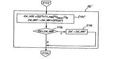
図13は割込ルーチンTIMER0_ROUTのフローチャートを示す。この割込ルーチンでは、ロータ110の回転数が過度に低いときポンピングが要求される。
【0121】
割込ルーチンTIMER0_ROUTはタイマ割込により呼び出される。このタイマ割込はμC23に組み込まれたタイマTIMER0により規則的間隔で形成される。タイマTIMER0は例えば1バイト(256ビット)の大きさであり、プロセッサ周波数が10MHzで、8のプレスケールの場合、タイマは256×8×0.4μs=820μs毎に値0に達し、タイマ割込が行われる。この0.4μsは、プロセッサ周波数が10MHzの際に1クロックが0.1μsを必要とし、プロセッサは各命令に対して4クロックを必要とする、すなわち0.4μsを必要とすることから生じる。これには同様にタイマTIMER0も同様に拘束される。
【0122】
S200は、割込ルーチンTIMER0_ROUTで実行される他の全てのステップに対する代理である。タイマTIMER0によって例えばリングカウンタCNT_HLも同様に増分される。このリングカウンタはホール時間t_HALLを計算するために使用される。
【0123】
S201では動作電圧UB(図23)の監視が、変数FCT_UBTを1にセットすることにより要求される。
【0124】
S202ではカウンタCNT_Pが1だけ減分される。
【0125】
S204ではCNT_Pが検査される。CNT_P>0の場合にはS210へ移行し、それ以外はS206へ移行する。
【0126】
S206では値FCT_PUMPが1にセットされる。このことによりメインプログラムにμC23(図25)で、ポンプ機能S604(図25)を呼び出すべきであることが通知される。その後、S210へ移行する。
【0127】
S210では割込ルーチンTIMER0_ROUTを去る。
【0128】
図14Aと図14Bは、タイマ割込ルーチンTIMER0_ROUT(図13)によって実行されるポンプ監視を示す。ホール信号HS256が上の線図では時間tに関してプロットされており、下の線図ではポンプカウンタCNT_Pの値266が時間tに関してプロットされている。ホール信号HSの各変化の際にポンプカウンタCNT_Pは値CNT_P_MAX(例えばCNT_P_MAX=11)にセットされる。その後、このカウンタは割込ルーチンTIMER0_ROUTでカウンタダウンされる。
【0129】
カウンタCNT_Pがゼロに達しなければ、モータ回転数は十分に高速であり、ポンプが保証される。
【0130】
しかしカウンタCNT_Pが例えば点267で値ゼロに達すると、割込ルーチンTIMER0_ROUTにより、μC23によりポンピングが要求される。初期値CNT_P_MAX=11の場合、カウンタCNT_Pは11×820μs=9ms後にゼロに達する。従ってポンピングは少なくとも11×820μs=9ms毎に行われる。
【0131】
制御器
図15は、μC23における制御器24のPI制御器としての実施例を示す。点270で瞬時の制御偏差(n_s−n)が、目標回転数n_sと実際回転数nとの差から計算される。
【0132】
点(ノード)280では3つの重み付けされた値が加算される。これは第1に、K1(例えばK1=30.38)により重み付けされた瞬時の制御偏差である。
【0133】
第2にこれはK2(例えばK2=―0.62)により276で評価された古い制御偏差である。ここで274のZ-1は、270からの先行の値を使用すべきであることを意味する。
【0134】
第3に古い調整値が284を介して280で加算される。このことによりいわゆるアンチ・ウインドアップが達成され、これは制御器24の改善のためにμC23で供給される。
【0135】
加算素子280からの結果は282で制限され、続いて286に調整値として出力される。
【0136】
K1とK2に対してはこの実施例では
K1=P+I=31 (5)
K2=−P=−30.38 (6)
が適用され、ここでPはPI制御器24のP成分、IはI成分である。従ってP=30.38(98%に相当する)、I=0.62(2%に相当する)である。
【0137】
図16は、図15の制御器24の実施形態のフローチャートを示す。
【0138】
S100で制御偏差RGLDIFFが目標値n_sと実際値nとの差から形成される。
【0139】
S102で古い制御偏差RGLDIFF_Oが評価される。この評価は、値RGL_I(例えば0×F9=249)との乗算と、引き続き256(0×0100)による除算によって行われる。RGLDIFF_Oは制御ルーチンで前もってすでに−1により乗算されている(S112)。結果は変数TEMP1に記憶される。
【0140】
S104では瞬時の制御偏差RGLDIFFと評価された古い制御偏差TEMP1とが加算され、値TEMP2に記憶される。TEMP2の符号は値VZ_TEMP2に確保される。TEMP2の絶対値は値RGL_VERSTと乗算され、TEMP3に記憶される。乗算によりP成分とI成分とが増幅される。この乗算の際にオーバフローが発生すると、S106からS107へジャンプする。
【0141】
S107ではVZ_TEMP2が検査される。VZ_TEMP2=1であれば、TEMP3がS109で最大値TEMP3_MAX(例えば全てのバイト0×FF)にセットされる。それ以外の場合、TEMP3はS108で0にセットされる。
【0142】
S110では新たな調整値SW(図15の個所280の値)がTEMP3と古い調整値SWとの加算により形成される。ここでオーバフローが発生すれば、調整値SWはSW_ABS_MAX(例えば全てのバイト0×FF)にセットされ、アンダーフローの場合は値SWがSW_ABS_MIN(例えば全てのバイト0×00)にセットされる。
【0143】
S112では瞬時制御偏差RGLDIFFがRGLDIFF_Oに制御器24の次のルーチン実行のために確保される。ここでは同時にRGLDIFFの符号が変化される。
【0144】
S112の後、制御器ステップ282で調整値制限が実行される(S114からS122)。
【0145】
S114では最小調整値SW_MINと最大調整値SW_MAXが計算される(CACL)。これら極大、極小の調整値については図20,22および図28で詳細に説明する。最大調整値にはオフセットOFFSET1が加算される。このオフセットは三角波発生器183(図9)の三角信号が電圧0Vのオフセット199を有する(図10A)ことから生じる。このオフセットは調整値SWにすでに含まれているが、計算された極大、極小の調整値SW_MINとSW_MAXには含まれていない。図30による変形実施例ではこのオフセットが省略される。これについては別個に説明する。
【0146】
S116では、調整値SWがSW_MIN’より小さいか否かが検査される。小さい場合にはSWがS118でSW_MIN’にセットされる。
【0147】
S120では、SWがSW_MAX’より大きいか否かが検査される。これが大きい場合にはSWはS122でSW_MAX’にセットされる。
【0148】
値SW_MIN’とSW_MAX’はS114に従い計算される。
【0149】
S124では、制限された調整値SWがPWM発生器25に引き渡される(PWMGEN1)。PWM発生器25は10ビットの分解能を有する。従ってSWのハイバイトの8ビットとローバイトの最高位2ビットが引き渡される(×により示されている)。残りのビットは使用されない(0により示されている)。
【0150】
この制御器24は非常に高い精度を有し、例えば10000回転/分の回転数において偏差は±1回転である。
【0151】
制御器24はそれぞれのモータ形式に、増幅係数RGL_I(S102)、RGL_VERST(S104)の変更によって適合しなければならず、変数の大きさを適切に選択しなければならない。それぞれの計算演算の際にオーバフロートとアンダーフローについて検査される。
【0152】
ソフトウエアによる電流制限
図17は、図3の別の簡単な等価回路を示し、図18は、例としてPWM信号PWM2を示す。この信号には参照符号180が付してある。同じ部材には先行図面と同じ参照符号が付してある。
【0153】
供給電圧UBは信号PWM2 180(図8)によりそのデューティ比tON/T(図18)に比例して低減される。生じた低減された電圧はUEとして示されている。近似的に
UE=UB*PWM2=UB*tON/T (7)
が成り立つ。
【0154】
固定子巻線116(図3)で永久磁石ロータ110の回転により誘導された電圧Uiは122の付された電圧源Mにより示されている。式(7)に従って誘導された代替電圧UEがこの誘導電圧Uiより大きければ、正の巻線電流i3が生ずる。Uiとi3の積は同様に正である。すなわちモータ32はエネルギーを消費して駆動される。
【0155】
しかし誘導された電圧Uiが代替電圧UEより大きければ、負の巻線電流i3が生じ、モータ32は制動される。なぜならモータは今度は発電機として動作するからである。図17に示された電流i3の方向は反転する。
【0156】
誘導された電圧Uiはしばしば、このようなモータの逆起電力(counter EMF)とも称される。その大きさは式(2)から得られる。
【0157】
図3と同じように図17には巻線抵抗Riが121により、巻線インダクタンスLが120により示されている。
【0158】
図19は、誘導された電圧Ui(図3)を回転数nについて曲線122として示す線図である。式(2)に従い
Ui=n*ke
が成り立つ。
【0159】
さらに2つの破線294,296がプロットされており、これらは最大および最小許容代替電圧UE,maxとUE,minを示す。これらの代替電圧は式(7)に従いデューティ比PWM2と電圧UBから生じる。nrevはリバース回転数であり、この回転数から、正の電流制限が存在する場合には、リバース、すなわち反対の回転方向に対するコミュテーションが可能である。
【0160】
以下詳細に、どのように制限曲線294と296が実現され、どのような意味を有するかを説明する。
【0161】
出力段78(図3)による巻線電流i3は、図17に従い抵抗121の電圧URiと抵抗121の値Riとから次式(18)に従って計算される。
i3=URi/Ri (8)
【0162】
比較的に長く通電した後、インダクタンスL120はもはや影響を及ぼさなくなり、抵抗121の電圧URiは
URi=UE−UI=UB*tON/T−n*ke=i3*Ri (9)
から得られる。
【0163】
ここから巻線電流i3に対して
i3=(UB*tON/T−n*ke)/Ri (10)
代替電圧UEに対しては
UE=n*ke+i3*Ri (11)
が成立つ。
【0164】
モータ32の固定子巻線116を流れる電流i3は出力段78を通電する際、すなわちこの出力段のトランジスタが制御される際にはクリティカルな量である。i3が過度に大きくなると、固定子巻線に大きな熱が発生し、最悪の場合、ロータ110(図1)の永久磁石がステータ114に生じた強い磁界により減磁されてしまい、このことによりもはやモータ32が機能しなくなる。従ってこの状態は阻止しなければならない。
【0165】
固定子巻線の最大電流Imaxはモータ動作の場合、通常はデータシートに記載されており、制動動作の際にこの許容電流は通常−Imaxである。
【0166】
ここから最大代替電圧UEmaxに対して
UEmax=n*ke+Imax*Ri (12)
同様に最小代替電圧UEminに対して
UEmin=n*ke−Imax*Ri (13)
が得られる。
【0167】
例えばモータ32が回転数0/分の際に、−Imax*Riと+Imax*Riとの間にある電圧UEにより駆動されると、電流i3はImaxより小さい。
【0168】
従ってモータ32に供給される代替電圧UEが曲線296と294の間の領域295(図19)にあれば、モータ32は安全な動作領域で動作する。すなわちロータ110は減磁されず、モータの固定子巻線は過度に加熱されない。
【0169】
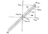
安全動作領域295の大きさ、すなわちUEminとUEmaxとの間の間隔は巻線抵抗121の値Riに強く依存する。この値が大きければ、モータ32は大きな安全動作領域195を有する。このようなモータはインピーダンス保護されたモータと称することができる。これとは反対に図19のモータはインピーダンス保護されないモータである。なぜなら安全動作領域295が非常に狭く、従ってこのモータが常にこの安全動作領域295で動作するように気を付けなければならない。
【0170】
図16の制御器では、本発明により調整値制限部282によって確実なソフトウエア的電流制限が実現される。この電流制限はモータ32をこの安全領域295に留める。
【0171】
このためにS114(図16)で値SW_MAXとSW_MINを瞬時回転数nの関数として次のように計算する:
SW_MAX:=UEmax(n) (14)
SW_MIN:=UEmin(n) (15)
【0172】
要求される精度に応じて、式(14)と(15)によるこの関数は大きく異なる構造を有することがある。以下簡単な実施例で、SW_MINとSW_MAXに対する近似値を計算する場合を説明する。SW_MAXとSW_MINに対する正確な値は図5から図7の構成を用いたアナログ電流制限部により設定される。ここでは電流i2が実際に測定される。
【0173】
しかし図19の構成は、電流i2を測定せずに実現することができる。なぜなら式(12)と(13)に従って特性曲線294と296はモータ32の回転数nの関数であり(電流i2の関数ではない)、この回転数nはμC23でホール信号HS1,HS2,HS3から既知だからである。式(4)を参照してμC23は各モータ回転数nに対して許容値UEmaxとUEminを計算する。この種の解決手段が図30に示されている。
【0174】
許容値UEmaxを上回ると、このことはデューティ比PWMがμC23(図30)の出力側で高すぎることを意味し、このデューティ比は制御器のソフトウエアにより相応に低減される。許容値UEminを下回ると、デューティ比PWMは出力端157(図30)でμC23により相応に高められる。なぜなら回転数が過度に低いからである。このことによりモータ32の電流i2は制限され、モータ32は常に限界内で回転する。この限界は図19で領域295によって設定される。
【0175】
大きな利点はこの場合、図8から図10のアナログ電流制限部を省略できることである。すなわちμC23はモータ32のいわゆる合成的(Synthetisch)モデル(モータ定数ke、許容電流Imax(駆動)ないし−Imax(制動)、および巻線抵抗Riにより合成的にモデル化したもの)を含み、これらの値と常時測定される回転数nに基づいてμC23はモータ32に対する調整値、例えば図30でのデューティ比PWMを計算する。この調整値は次にモータ32の制御に直接用いることができ、デューティ比として図11の入力端180に直接供給される。このことにより図30では、図8から図10のアナログ電流制限装置が省略される。
【0176】
モータ32のこのような合成的モデルはさらに別の変数を考慮することができる。これは例えばモータ32の熱容量である。すなわち図19の領域295を、ロータ110の減磁の危険が存在しない限り短時間去ることもでき、このことにより例えばモータ32の急速な起動が可能となる。
【0177】
モータ定数ke、駆動時の最大許容電流Imaxおよび制動時の最大許容電流−Imax、並びに巻線抵抗121の値Riは、μC23のプログラムに定数として記憶するか、または外部から制御器に入力することができ、これは例えば図示しないEEPROMで相応の値を変更することにより行う。これについては1998年6月13日出願のドイツ特許出願(公開)19826454.5を参照されたい。
【0178】
図20は図16の制御器のステップS114の可能な実施例を示す。SW_MINとSW_MAXを計算するために式(13)、(15)ないし(12)、(14)を使用する。
【0179】
ソフトウエアにより支援された電流制限
図21は、図19と同様に線図を示す。ここでは誘導された電圧Ui122が回転数nについてプロットされている。ラインUE,min296とUE,max294は図19のそれらに相応し、従ってUiを中心とする領域295を画定する。この領域内ではモータ32が確実に動作することができる。
【0180】
モータ32の両方の回転方向に対しては、回転数nの絶対値による1つの線図が必要なだけである。なぜなら例えば3相モータの場合、他方の回転方向に対する相違はコミュテーションの形式が別であるだけだからである。回転数nをホール時間t_HALLから計算すること(図12)は回転方向に依存しない。
【0181】
図20でのSW_MINとSW_MAXの計算は乗算および場合により除算を含む。これらは使用されるμC23で高い計算工数、ひいては時間を必要とする。
【0182】
図16の調整値制限部282dでの計算工数を低減するために例えば、調整値をまず最初に下方についてだけ制限し、次に簡単な計算を使用することができる。
【0183】
図21は直線298を含む。この直線は座標系の原点を通る。直線298は最大アイドリング回転数n_maxの際に例えば最大誘導電圧の半分Umax/2に達する。この直線は調整値SW_MINの限界を表し、モータ32が制動するとき、すなわち発電機として動作するときに作用する。すなわち制動動作時には調整値はこの値を下回ることはできず、これにより制動電流が制限される。
【0184】
図22は、調整値制限282’のフローチャートである。この調整値制限は、図16の調整値制限282とは反対に調整値SWを下方の方向SW_MIN’についてだけ制限する。従って図16のステップS120からS122は省略される。
【0185】
最小調整値SW_MINのS114”での計算は図21の直線298に従い、次式ににより行われる。
SW_MIN:=(1/2*n/n_max)UNenn/UB (16)
【0186】
UNennはモータの公称電圧であり、n_maxは公称電圧UNennにおける最大アイドリング回転数である。
【0187】
従って下方への簡単な調整値制限が得られ、この制限は図7のようなハードウエア電流制限部を支援する。
【0188】
ハードウエア電流制限とソフトウエア電流制限との組合せは別の利点を有する。ソフトウエア電流制限により最大制動電流i2’を、これが最大許容電流よりやや(僅かに)上になるように調整することができる。ハードウエア電流制限部はこの過度に大きな電流i2’を検知し、これをさらに制限する。従ってモータ32が最大出力に達することが保証され、同時にモータの公差が捕捉される。このようにして非常に高速な制御過程が得られる。
【0189】
負の電流制限に対しては図6で説明したように、最小デューティ比SW_MIN_CONSTを維持しなければならない。これは制動電流i2’の測定を可能にするためである。図21,22では回転数に依存する最小調整値SW_MIN(n)が維持されるから(直線298参照)、図6で説明した一定の最小調整値SW_MIN_CONSTは省略される。これによりモータ32の制御領域が拡大される。
【0190】
SW_MINとSW_MAXの計算を簡単にする別の手段は、調整値SW_MINとSW_MAXを回転数nに依存してテーブルに記憶することであり、場合によりテーブル値間を補間することである。
【0191】
SW_MINとSW_MAXの計算を簡単にするためのさらなる手段では、値UNenn/UBを一定の係数、例えば値1と見なす。この簡素化は、値UBがUNennから大きな偏差を有しないときに可能である。このことにより除算ひいては計算時間が節約される。
【0192】
さらなる計算時間は次のことにより節約される。すなわち乗算をシフト演算により置換するのである。変数を1桁だけ左にそれぞれシフトすることにより2による乗算が達成され、1桁だけ右にシフトすることにより2による除算が達成される。
【0193】
動作電圧の監視
図23はサブプログラムUB_TESTを示す。このサブプログラムは、図1の端子76で測定することのできる動作電圧UBを監視するのに使用される。UBが許容領域外にあれば、フルブリッジ回路78が相応に制御され、これにより中間回路73,74に接続された構成部材、例えば電力トランジスタ80〜85,フリーホイールダイオード90〜95、コンデンサ75および構成部材77(図1)は破壊されることがない。
【0194】
サブプログラムUB_TESTは機能マネージャ603(図25)により、変数FCT_UBTが1にセットされるときに呼び出される。サブプログラムUB_TESTの要求はS201(図13)の割込ルーチンTIMER0_ROUTで行われる。
【0195】
S302では変数FCT_UBTが再び0にリセットされる。
【0196】
S304では、A/D変換器(μC23内の)を介して、μC23の入力端63の電圧の高さが問い合わされ、デジタル値として変数U_ADに記憶される。
【0197】
図24は、例としてデジタル量U_ADの時間経過を示す。このデジタル量はアナログ量UB(=モータ32の動作電圧)に相当する。値U_ADは非常に小さくなることがある。なぜなら例えば電気自動車では蓄電池が放電されるからである。次に動作電圧が下側限界値U_MIN_OFFより低下すると、モータ32は自動的に遮断されなければならない。この電圧が比較的に高い下側限界値U_MIN_ONを超えると、モータ32を再び投入接続することができる。これにより下側切り替えヒステリシスが得られる。
【0198】
制動時に、例えばモータ32が発電エネルギーをコンデンサ75にフィードバックすることにより量U_ADが過度に大きくなると、その結果、そこで電圧UBが上昇する。なぜならこのエネルギーは負荷77により消費することができないからである。電圧UBが過度に上昇することは阻止しなければならない。なぜならそのようにしないと、構成部材77が破壊されてしまうからである。
【0199】
図24の340には、モータ32の制動過程により発生した、量U_ADの上昇が示されている。342では上側閾値U_MAX_OFFを上回り、モータ32の全てのトランジスタ80〜85が阻止される。このことにより344で値U_ADが低下し、346で比較的に低い閾値U_MAX_ONに達する。この閾値ではトランジスタ80〜85のコミュテーションが再び通常のように投入される。その結果348で量U_ADは再び上昇する。350ではトランジスタ80〜85が新たに阻止される。その結果352で値U_ADは新たに低下し、352で閾値U_MAX_ONに再び達する。ここで再びモータ32のコミュテーションが投入される。この例では制動過程が今や終了する、なぜならモータがその目標回転数n_sに達するからである。そして値U_ADはさらにU_ADの「通常」値354まで低下する。この通常値は「安全領域」356にある。
【0200】
図24では360により過度に低い動作電圧UBによる「禁止領域」が示されており、362により過度に高い動作電圧UBによる禁止領域が示されている。この領域は通常では制動時に発生し得る。
【0201】
図23のプログラムは上に述べたプログラム経過の実現に用いる。ステップS306からS308で、量U_ADがU_MIN_OFFとU_MAX_OFFとの間にある許容領域から外れたか否かが検査される。外れていればS310へジャンプし、それ以外ではS320へジャンプする。
【0202】
S310では変数U_OFFに基づいて、出力段78がすでに遮断されているか否かが検査される。遮断されていれば、すなわちU_OFF=1であれば、直ちにS330の終了へジャンプする。それ以外の場合、S312でU_OFFが1にセットされ、全ての信号EN1,EN2,EN3(図8)がHIGHにセットされる。これにより全てのブリッジトランジスタ80〜85(図1)は非導通に制御される。巻線115,116,117に誘導された電圧78は電力スイッチ80〜85が開放しているときコンデンサ75の電圧UBより下にあるから、全てのフリーホイールダイオード90〜95は阻止されており、電流ひいては電力がモータ32から中間回路73,74へ流れることはない。モータ32は従って「自由切り替え」状態に(freigeschaltet)される。すなわちモータは電力を消費することも、出力することもしない。
【0203】
S320からS322では、U_ADが許容領域356内にあるか否かが検査される。ステップS306とS308で定義された非許容領域よりも小さいこの許容領域356によって電流制限のヒステリシスが得られる。このことはモータの動作特性を改善する。ヒステリシスが必要なければ、S324をS308の選択肢「N」に直接続けさせ、ステップS320,S322を省略することができる。
【0204】
U_ADが許容領域356内にあれば、S320ないしS322からS324へジャンプし、それ以外の場合はサブプログラムUB_TESTをS330で終了する。
【0205】
S324では、U_OFFがすでに0であるか否か、すなわち出力段78がすでに通常にコミュテーションされているか否かが検査される。U_OFF=0であれば、終了S330へジャンプし、それ以外の場合はS326で変数U_OFFが0にセットされ、COMMUTで出力段78は図2のテーブルに従い通常のようにホール信号HS1,HS2,HS3に依存してコミュテーションされる。このことは以下、図29で説明する。ここではコミュテーションの開始を回転数の上昇と共に進み方向にずらすこともできる。これについてはDE19700479A1を参照されたい。
【0206】
このようにしてモータ32は制動時に、すなわちモータが回転数制御器により設定された所望の回転数n_sを上回るときにエネルギーを自動的にコンデンサ75(図1)にフィードバックし、このときにコンデンサの電圧UBが非許容値を取ることはない。
【0207】
同じように、モータの動作電圧UBが許容値U_MIN_OFFを下回るときにはモータ32の遮断が保証される。このことによりモータ32の誤機能が回避される。このことはとりわけこのようなモータが図示しない蓄電池により駆動される場合に重要である。蓄電池は図1の整流器72の個所にあると考えることができ、当業者には自明である。
【0208】
サブプログラムCOMMUT(図29)では、さらなる障害が存在しない場合、出力段78がホール信号HS1,HS2,HS3に依存してコミュテーションされる。一般的にコミュテーションにも用いられるサブプログラムCOMMUTはコミュテーションの際にU_OFFの値を考慮する。U_OFFが値1を有していれば、全ての信号EN1,EN2,EN3(図8)はHIGHに留まる。図29のS330を参照。
【0209】
機能マネージャ
図25は、μC23で実行される、いわゆる機能マネージャの形態のメインプログラムの可能な実施例のフローチャートを示す。
【0210】
メインプログラムのタスクは、例えばロータ位置信号HS1,HS2,HS3の1つの変化などのイベントに応答し、さらに必要な場合に各機能にリソース、とりわけ計算時間を提供し、リソースの設定の際に優先度に注意を払うことである。
【0211】
モータ32のスイッチオンの後、μC23で内部リセットがトリガされる。S600でμC23の初期化が行われる。場合により時間的にクリティカルな他のプログラム経過が実行される。これはS601で示されている。
【0212】
その後、機能マネージャ603へジャンプされ、この機能マネージャはS602でスタートする。機能マネージャ603は個々のサブプログラムの経過を制御し、それらの優先度を決定する。
【0213】
図26は、例としての機能マネージャ605を示す。ここではサブプログラムS604,S610,S614,S618およびS622の各々に対して1ビットがリザーブされている。
【0214】
この実施例では機能レジスタ605は1バイトの大きさであり、低位ビット(LSB)から始まって次の要求ビットを下で説明する要求可能な機能に対して定義する:
・Bit1:目標回転数n_sをμC23の入力端48におけるアナログ電圧値から計算するためのFCT_n_S、
・Bit2:任意の形式の制御ルーチンに対するFCT_RGL、
・Bit3:実際回転数nを計算するためのFCT_n、
・Bit4:ホール時間t_HALL(図12参照)を計算するためのFCT_HL、
・Bit5:μC23によるポンプ(図23参照)のためのFCT_PUMP、
・Bit6:動作電圧UBの監視のためのFCT_UBT。
【0215】
残りのビットは付加的に要求可能な機能のためにリザーブされている。これらの機能は必要に応じて機能マネージャ603に挿入することができる。
【0216】
所定の要求可能な機能を、他の機能または割込ルーチンにより要求すべき場合、要求される機能のビットが1にセットされる。例えばFCB_UBT:=1となる。機能マネージャ603が、この要求に続くプログラムルーチンでそれより高い優先度を有する他の要求可能な機能を発見しなければ、この場合は動作電圧の監視に対する機能が実行される。これは図23に示されている。
【0217】
要求された機能が処理されると、この機能はそのビットを機能マネージャ603で再び0にセットする。例えば図23のS302でのFCT_UBT:=0である。
【0218】
図25ではS602の後に所定の順序(最重要な要求可能機能から始まって)で、それらの要求ビットがセットされているか否かが検査される。1つの機能でセットされていれば、これが実行され、これに基づき再びステップS601へジャンプする。機能マネージャ605での検査順序は要求可能な機能の優先度を設定する。機能が機能マネージャ603で比較的に高い位置にあれば、その機能の優先度は高い。
【0219】
S602で、ポンプに対する要求ビットFCT_PUMPがセットされているか否か、すなわち値1を有するか否かが検査される。セットされていれば、S604へジャンプし、ポンプ機能(図15の説明)が実行される。終了の前にポンプ機能はその要求ビットFCT_PUMPを再びゼロにリセットする。その後、ステップS601へジャンプする。
【0220】
S602でFCT_PUMPがセットされていなければ、S608でFCT_UBTがセットされているか否かが検査される。セットされていれば、機能S610(図23,24)で動作電圧UBの監視が呼び出される。
【0221】
同じようにしてFCT_nがセットされている場合には、S612から実際回転数n(図12)の計算機能S614が呼び出される。FCT_RGLがセットされている場合には(S616)制御機能D618(図16)が呼び出され、FCT_n_sがセットされている場合には(S620)目標回転数n_sの計算機能(図8)が呼び出される。
【0222】
S602からS620で検査されるいずれのビットもセットされていなければ、S620から再びS601へジャンプする。すなわちS601は各ループの経過の際に実行される。
【0223】
図25は624に象徴的にホール割込を示す。このホール割込は最高の優先度(レベル1)を有する。ホール割込がこの高い優先度を有するのは、ホール信号の正確な検出がモータ39の静粛な回転に対して非常に重要だからである。ホール割込は機能マネージャ603の全てのプロセスを中断する。これは矢印626により象徴的に示されている。
【0224】
ホール割込624の下にはタイマTIMER0のTIMER0割込が示されている。この割込は次に低い優先度L2を有しており、その下にある全てのプロセスを中断する。これは矢印630により示されている。
【0225】
次に低い優先度はポンプ機能S604が有する。なぜならポンピングはモータの確実なコミュテーションに対して重要だからである。
【0226】
次に低い優先度L4は電圧監視機能S610が有する。この電圧監視機能は、過度に高い動作電圧によるモータ32の破壊を阻止する。
【0227】
次に低い優先度L5は、実際回転数nの計算機能S614が有する。実際回転数nは目標回転数n_sよりも頻繁に変化する。
【0228】
次に低い優先度L6は制御機能S618が有し、最低位の優先度は目標回転数n_sの計算機能S622が有する。
【0229】
しかし場合によりステップS602〜S620の順序、およびそれらの優先度を入れ替えることもできる。
【0230】
例えばモータ32と(図示しない)デスクトップコンピュータとの間の通信を制御する機能S601が存在する場合には、これはL2とL3の間の優先度を有する。
【0231】
このようにしてモータ32の種々異なる「必要性」を所定の階層に配列し、μC23のリソースをモータの動作に対して最適に使用することができる。
【0232】
図27は、図19および21のような線図を示す。ここでは誘導された電圧Ui122が回転数nに対してプロットされている。ラインUE,min296とUE,max294は図19のそれに相応し、従ってUiの周囲の領域295を制限する。この領域内ではモータ32の確実な動作が可能である。
【0233】
図20でのSW_MINとSW_MAXの計算は乗算および場合により除算を含む。これらは使用されるμC23で高い計算ステップ数および長い時間を必要とする。
【0234】
図16の閾値制限S113での計算ステップ数を低減するために、簡単な計算が使用される。上側限界線299と下側限界線298は直線として示されており、それぞれオフセットc_minないしc_maxをn=0回転/分の個所で有する。この例ではc_min=0である。
【0235】
直線298は図21のように最大アイドル回転数の際に例えば最大誘導電圧の半分Umax/2に達する。この直線298は調整値SW_MINの限界を表す。直線299は、例えば最大回転数の半分n_max/2で最大電圧Umaxに達する。この直線は調整値SW_MAXの限界を表す。
【0236】
図28は、図16の制御器のステップS144の可能な実施S114'''を示す。これは図27の直線に対するものである。一般的な直線式が選択される。
SW_MIN:=m_min*n+c_min
SW_MAX:=m_max*n+c_max
【0237】
m_minは直線298の勾配であり、m_maxは直線299の勾配である。c_minは直線298の縦軸交点(この例ではc_min=0)であり、c_maxは直線299の縦軸交点である。
【0238】
定数c_max,c_min,m_max,m_minを任意の選択することにより、例えば記憶された値を変更することにより、モータの特性を簡単に変更することができる。
【0239】
c_minは負に選択することもできる。c_maxは小さく選択することができ、これによりモータ32を緩慢に起動させることができる。このようにすると、目標回転数n_sに達する際の過励振(モータ回転数の回転振動)が回避される。同じように直線299を、直線294と直線122との間の領域におくことができる。これにより非常に確実な電流制限が得られる。
【0240】
図29はサブプログラムCOMMUTを示す。このサブプログラムは出力段78(図1)のコミュテーションを、図2のコミュテーションテーブルに従い、制御回路50,52,54(図8)によって実行する。点火角シフトを行わないモータではこのサブプログラムは例えばホール割込ルーチンによって呼び出される。
【0241】
S302では電圧監視UB_TEST(図23)に基づいて、出力段が遮断されたか否かが(U_OFF=1)検査される。遮断されていることは、中間回路73,74における電圧が過度に高いかまたは低いことを意味する。
【0242】
この場合S330へジャンプする。S330では、全てのドライバ構成素子200が非アクティブにされる。このことは出力端EN1,EN2,EN3を1にセットすることにより行われる。
【0243】
S332では、信号IN1,IN2,IN3が1にセットされる。このことはドライバ構成素子200が非アクティブである際には何の影響も及ぼさないが、記憶されたままの信号IN1,IN2,IN3の状態がこのことにより後続の過程に対して定義される。
【0244】
これに基づいて終了S340へジャンプする。
【0245】
S302でU_OFF=0であれば、すなわち中間回路73,74の電圧が正常であれば、通常のコミュテーションが図2のコミュテーションテーブルに従って行われる。
【0246】
S304で、図13でポンプ監視に使用されるカウンタCNT_PがCNT_P_MAXにセットされる。なぜなら以降、コミュテーションされるからである。
【0247】
S306では、信号EN1〜EN3に対する目標値EN1_S,EN2_S,EN3_Sが、ホール信号HS1,HS2,HS3の組合せHL_COMBに相応して図2のテーブルからロードされる。図2からのテーブル値にはTEN1,TEN2,TEN3が付してある。例えばロータ110が角度位置0゜...60゜elにあるとき、ホール信号の組合せHL_COMBは(HS1=1,HS2=0,HS3=1)であり、次の値がロードされる:EN1_S=0、EN2_S=0,EN3_S=1。
【0248】
同じようにS308で信号IN1〜IN3に対する目標値IN1_S,IN2_S,IN3_Sが、ホール信号HS1,HS2,HS3の組合せHL_COMBに相応して図2のテーブルからロードされる。IN値に対するテーブルにはTIN1,TIN2,TIN3が付してある。S306からの例に対しては、IN1_S=1,IN2_S=TRISTATE、IN3_S=1が角度位置0゜...60゜elに対して得られる。
【0249】
コミュテーションの前には、ドライバ構成素子の2つがアクティブであり、1つが非アクティブであった。例えば図8のコミュテーションの前には、構成素子52と54がアクティブであり、構成素子50が非アクティブであった。コミュテーション後には、例えば構成素子54が非アクティブであり、構成素子50と52がアクティブになる。
【0250】
ステップS310からS320は、コミュテーション前にアクティブであったドライバ構成素子の遮断に用いる。この構成素子はコミュテーション後には非アクティブにすべきであり、上記の例では構成素子54である。コミュテーションの前後でアクティブである構成素子は常時、アクティブされたままである。このことによりモータ32での電力損失が回避される。
【0251】
図2では行EN1,EN2,EN3のそれぞれのフィールドにフレーム740が設けてある。ここではそれぞれのドライバ構成素子が順次連続する2つの角度領域でアクティブである。
【0252】
従ってS310で、信号EN1に対する目標値EN1_Sが1であるか否か、すなわちEN1をコミュテーション後に遮断すべきか否かが検査される。そのような場合には、EN1がS312で1にセットされ、巻線端子L1のブリッジ分岐路のドライバ構成素子が非アクティブにされる。EN1がコミュテーションの前に非アクティブであったとき、新たな非アクティブ化は何の作用も及ぼさない。
【0253】
S314からS320で、巻線端子L2とL3のブリッジ分岐路に対して同じことが行われる。
【0254】
S322では信号IN1,IN2,IN3が目標値IN1_S、IN2_S、IN3_Sにセットされる。
【0255】
S324では信号EN1,EN2,EN3が目標値EN1_S、EN2_S、EN3_Sにセットされる。コミュテーション後に非アクティブにすべきドライバ構成素子はすでにS310からS320で非アクティブにされているから、S324は以前に遮断されていたドライバ構成素子のスイッチオンに作用する。コミュテーションの前でも後でもスイッチオンされている他のドライバ構成素子はS310からS320で遮断されない。これは電流中断の際に発生することとなるモータ32での電力損失を回避するためである。
【0256】
S340でサブプログラムCOMMUTは終了する。
【0257】
モータ32を場合により両方向で回転させるためには、第2のコミュテーションテーブルを他方の方向に対して図2と同様に入力しなければならない。しかし多くの場合、例えばラジアルファンでは1回転方向の動作しか要求されない。反対の方向に対するコミュテーションテーブルによる動作は当業者には問題なしに可能であり、従って詳細には説明しない。
【0258】
図30は本発明の電子コミュテーション式モータ32の別の実施例の概観を示す。このモータは図8に類似する。同じ部材または同じに作用する部材には同じ参照符号が付してあり、通常は再度説明しない。
【0259】
図30では電流制限器131および161によるハードウエア電流制限部が省略される。これらはμC23で実行されるプログラムによって引き継がれる。このことは199により象徴的に示されている。ここでは例えば図16と同様の制御が使用される。この制御ではSW_MINとSW_MAXの計算が図27および28と同様に実行され、このとき直線298と299は直線UEmin296とUEmax294に夫々重なる。図28のオフセットOFFSET1はここでは0である。なぜならPWM発生器182が省略されているからである。
【0260】
交互の(パルス立上り)クロッキングに必要なPWM信号PWM181は、ハードウエア電流制限部131,161が使用されないから、μC23の出力端157から直接、制御回路50,52,54に供給され、所要の電流制限を行う。従ってモータ32は安全領域295でだけ駆動することができる。モータ電流の測定はここでは省略される。非常に有利には、電流の値を回転数に依存して制限することができる。これにより例えば穏やかな起動が得られる。
【0261】
図31は図3の別の電気的等価回路を示す。この回路は図1のフルブリッジ回路78の一部だけを示す。同じ部材または同じに作用する部材には同じ参照符号が付してあり、通常は再度説明しない。
【0262】
図31では、図3で閉じていた上側電流スイッチ82の代わりに、下側電力スイッチ83が閉じている。さらにクロッキングされる制御信号228が上側電力スイッチ80に、クロッキングされる制御信号227が下側電力スイッチ81に印加される。
【0263】
出力段78のこの形式の通電での主たる相違は、ロータ110の所定の角度領域に対してスイッチオンされる電力スイッチが図31では下側電力スイッチ83であり、図3では上側電力スイッチ82であることである。相応にして、クロッキングされる電力スイッチ80と81の制御も入れ替わり、適合したテーブル(図2)を制御論理回路に使用しなければならない。
【0264】
信号227,228を形成するためにここでは変更は行われない。従って本発明のモータの前記特徴は全て同じようにこの実施例に適用される。
【0265】
信号IN1,IN2,IN3の必要な変更は図32に示されている。
【0266】
この回路の利点は、下側電力スイッチ83を使用することによってL2のブリッジ分岐路もポンピングされることである。その他の機能は同じであり、電流i3は(図3参照)は反対方向に流れる。
【0267】
図32は図8の変形実施例を示す。図32の回路は図31の変形実施例の制御に使用される。示されているのは図8からの変更部分である。他の全ての部分は図8の部分に相当し、図示されていない。
【0268】
図8のツェナーダイオード186は除去されており、図8のダイオード260は反対に極性付けられており、参照符号260’を有する。図8の抵抗262はアースに接続されているのに対し、抵抗262’は+Vccに接続されている。
【0269】
図32により、下側電力スイッチを次のことによって調整することができる。すなわち、IN1,IN2またはIN3をゼロにセットすることによって調整することができる。図8の回路では、信号IN1,IN2またはIN3のセットにより信号PWM2 180がそれぞれダイオード(260)を介してアースに引き込まれる。
【0270】
従って図32ではダイオード260’が使用され、これにより線路IN1はダイオード260’によってアースに対して(gegen)引き込まれる。
【0271】
これによりμC23は、IN1(IN2,IN3)をゼロにセットすることによりそれぞれ下側電力スイッチをスイッチオンし、IN1(IN2,IN3)をTRISTATEにセットすることによりPWM信号PWM2 180を導入することができる。PWM信号はこのためにPWM発生器182’で反転される。
【0272】
もちろん本発明の枠内で多種多様の変更および変形が可能である。
【0273】
ある電子コミュテーション式モータでは駆動電流(i2)も制動電流(i2’)と同じように監視される。駆動電流が過度に大きい場合には、モータの電流を制御するデューティ比が低減される。そして制動電流が過度に大きい場合にはこのデューティ比が高められる。このために2つの電流制限素子(131,161)を備えるアナログ回路があり、同様にこの機能をマイクロコントローラのソフトウエアにより実現し、従って電流測定を省略することのできる回路を有する。さらに2つの手段を組み合わせることもできる。ここではハードウエア電流制限とソフトウエア電流制限とが共働で作用する。
【図面の簡単な説明】
【図1】 図1は、本発明の電子コミュテーション式モータの第1実施例の概略的回路図である。
【図2】 図2は、ロータ位置センサの出力信号と、これに依存する図1のフルブリッジ回路78の制御を示す図である。
【図3】 図3は、本発明をよりよく説明するため、図1のフルブリッジ回路78の一部だけを示す等価回路である。
【図4】 図4Aから4Fは、図3に発生する電圧、電流および電力を交互クロッキングにおいて概略的に示す線図である。
【図5】 図5は、図1のモータでの駆動電流を制限するための電流制限装置である。
【図6】 図6は、図1のモータでの制動電流を制限するための電流制限装置である。
【図7】 図7は、図1のモータでの駆動電流と制動電流とを制限するための組み合わされた電流制限装置である。
【図8】 図8は、本発明のモータの有利な実施例を説明するための概略的回路図である。
【図9】 図9は、図8のモータに有利に適用することのできるアナログPWM発生器を説明するための概略図である。
【図10】 図10Aと10Bは、図9を説明するための線図である。
【図11】 図11は、図8の装置でのブリッジ分岐路の制御を説明するための詳細図である。
【図12】 図12は、図1のロータ位置センサ111,112,113の出力信号及び、組み合わされたロータ位置信号を示す図である。
【図13】 図13は、本発明のモータにおけるいわゆるポンピング経過を示すフローチャートである。
【図14】 図14Aと14Bは、図13の作用を説明するための線図である。
【図15】 図15は、デジタル回転数調整(制御)装置の作用を、これが本発明でどのように有利に使用できるかについて説明する基本図である。
【図16】 図16は、図15の調整装置を実現するためのフローチャートである。
【図17】 図17は、図16のフローチャートを説明するための極端に簡素化された装置の図である。
【図18】 図18は、PWM信号およびここで発生する信号形状と時間を示す線図である。
【図19】 図19は、先行図面の電子コミュテーション式モータを説明するためのモータ線図である。
【図20】 図20は、図16の調整装置の変形として使用することのできるフローチャートの1ステップを示す図である。
【図21】 図21は、簡素化された電流制限を説明するためのモータ線図である。
【図22】 図22は、図16の調整装置で変形として使用することができ、図21の実現のために用いられるフローチャートの一部である。
【図23】 図23は、モータの駆動電圧UBの制限を説明するためのフローチャートであり、この駆動電圧はモータに直流中間回路を介して供給される。
【図24】 図24は、図23のフローチャートを説明するための概略図である。
【図25】 図25は、有利には本発明のモータで使用することのできる機能マネージャである。
【図26】 図26は、8ビットの制御ワードであり、これは機能マネージャ(図25)で本発明のモータでのプログラム経過の実行に対して優先度を設定するのに使用される。
【図27】 図27は、電流制限の非常に有利な変形を説明するためのモータ線図である。
【図28】 図28は、図16の調整装置で変形として使用することができ、図27の変形を実現するために用いられるフローチャートの1ステップを示す図である。
【図29】 図29は、出力段78の転流に使用されるコミュテーション機能に対するフローチャートである。
【図30】 図30は、合成的モータモデルにより動作する図1の構成の有利な変形実施例を示す図である。
【図31】 図31は、図1のフルブリッジ回路78の一部だけを示す図3のような電気的等価回路であり、ブリッジの制御の他の形式の係るものである。
【図32】 図32は、図8の変形実施例であり、これは図31の変形実施例を制御するために必要である。[0001]
【Technical field】
The present invention relates to an electronic commutation motor having a permanent magnet rotor and a stator.
[0002]
[Technical background]
This type of electronic commutation motor is well known.
[0003]
[Problems to be solved by the invention]
An object of the present invention is to provide a novel electronic commutation motor.
[0004]
[Solution]
According to the present invention, this problem is an electronic commutation motor having a rotor and a stator,
A stator winding device and a commutation device;
The stator winding device can be fed with a current from a direct current source via a full bridge circuit,
The full bridge circuit has one upper MOSFET transistor and one lower transistor in each bridge branch;
The upper MOSFET transistor is connected to a positive line of a direct current source;
The lower transistor is connected to the negative line of the DC source;
The commutation device commutates the transistor;
In the commutation device, only one transistor is switched on in the first bridge branch depending on at least the rotor position, and the upper and lower transistors are controlled by the PWM signal in the second bridge branch. Are configured to be switched on alternately,
Further, depending on at least one motor amount, when a braking current exceeding a predetermined value is generated in the bridge circuit, the duty ratio of the PWM signal is changed to reduce the current generated by the motor in a power generation manner. The problem is solved by an electronic commutation motor provided with a device configured to do so.
[0005]
This type of electronic commutation motor is very suitable for operating tasks where the desired rotational speed can be exceeded by external influences. This ensures that this type of motor automatically shifts to a braking operation by means of a bridge circuit, which does not exceed or substantially does not exceed a predetermined motor limit value.
[0006]
Another means for solving the above problem is an electronic commutation motor including a rotor and a stator,
Having a stator winding device,
The stator winding device is fed with current from a DC source via a full bridge circuit,
The full bridge circuit has one upper NMOS transistor and one lower transistor in each bridge branch,
The upper NMOS transistor is connected to the positive line of the DC source;
The lower transistor is connected to the negative line of the DC source;
A storage capacitor is assigned to each upper transistor in the bridge branch.
The storage capacitor is chargeable via the lower transistor of the bridge branch and is used to supply a control voltage to the upper transistor;
And a commutation device for commutating the transistor,
In the commutation device, depending on at least the rotor position, only one transistor is switched on in the first bridge branch and the upper and lower transistors are alternately switched on in the second bridge branch. Configured to
When the motor speed is monitored and falls below a predetermined numerical value, after a predetermined time has elapsed, the upper transistor of the full bridge circuit is blocked for a short time, the lower transistor of the full bridge circuit is switched on for a short time,
This charges the storage capacitor of the upper transistor, so that reliable control of the upper transistor is obtained with an electronic commutation motor that is guaranteed even when the speed is low or even when the motor is stationary.
[0007]
Therefore, in a motor having this type of full bridge circuit using NMOS transistors, the driving capability is ensured even when the rotational speed is very low or even drops to zero.
[0008]
The means for solving the problems includes driving an electronic commutation motor having a permanent magnet rotor, a stator, a stator winding device, a commutation device, a microprocessor or a microcontroller, and hereinafter referred to as a microprocessor. A method,
The stator winding device can be fed with a current from a direct current source via a full bridge circuit,
The full bridge circuit has a plurality of bridge branches, each bridge branch having one upper MOSFET transistor and one lower transistor,
The upper MOSFET transistor is connected to a positive line of a direct current source;
The lower transistor is connected to the negative line of the DC source;
The commutation device commutates the transistor;
And the commutation device depends on at least the rotor position, and only one transistor is switched on in the first bridge branch, and is controlled by the PWM signal in the second bridge branch. In a method for driving a motor configured to be switched on alternately with a transistor,
The microprocessor monitors whether or not the DC voltage supplied to the motor has a predetermined relationship with the voltage induced by the motor based on a synthetic model of the motor.
If the relationship is not maintained, the duty ratio of the PWM signal is changed accordingly to correct the relationship,
The PWM signal alternately switches on the upper and lower transistors of the second bridge branch,
It can also be obtained by a method of driving an electronic commutation motor that acts against the deviation of the predetermined relationship by changing the duty ratio.
[0009]
Thus, by composing the software accordingly, i.e. a synthetic (and possibly simplified) model of the motor, the motor operates in an area that is not threatened by overload. For example, in many motors having high intrinsic power, a strong magnetic field is formed in the stator due to an excessively high driving current or braking current, and the permanent magnet rotor may be demagnetized. This is easily prevented by the method of the present invention, which significantly improves the operational reliability.
[0010]
Another solution to the above problem is an electronic commutation motor having a rotor and a stator,
A stator winding device is disposed on the stator,
The stator winding device is assigned a full bridge circuit having a plurality of bridge branches connected in parallel.
Each of the bridge branches has one upper transistor and one lower transistor;
The upper transistor is connected to the positive line of the DC source;
The lower transistor is connected to the negative line of the DC source;
One control circuit is assigned to each of the two transistors in the bridge branch path.
The control circuit is activated or deactivated depending on the first input signal and blocks two transistors of the assigned bridge branch in the inactive state;
The control circuit is switchable so that either the upper transistor or the lower transistor is controlled to be conductive when activated by the first input signal, depending on the second input signal.
And a microprocessor or microcontroller, hereinafter referred to as a microprocessor,
The microprocessor forms a first input signal at a first output end, forms a second input signal at a second output end,
And having a third input signal in the form of a PWM signal with a controllable duty ratio,
The third input signal can be supplied to the control circuit from the PWM signal source in parallel with the second input signal, and acts only when the second output of the microprocessor is switched to a predetermined switch state. Obtained by an electronic commutation motor.
[0011]
As a result, the PWM signal is successfully introduced for the first time immediately before the control circuit. This makes the circuit very simple, but the microprocessor nevertheless has full control over the control circuit. Thereby, the microprocessor can control the upper and lower transistors of the assigned branch branch without depending on the PWM signal (for example, when used as a charge pump). On the other hand, however, after switching the second output of the microprocessor to a predetermined circuit state, this bridge branch can be controlled by means of a PWM signal, for example to adjust motor parameters.
[0012]
Further details and advantageous embodiments of the invention emerge from the following description and the examples given in the drawings and from the dependent claims. However, the examples are not to be understood as limitations of the invention.Accordingly, the drawing reference numerals (and figure numbers) attached to the claims are only for helping the understanding of the invention, and are not intended to limit the present invention to the illustrated embodiment. Here is a preferred embodiment of the present invention:
(Embodiment 1) An electronic commutation motor having a rotor and a stator according to the first aspect of the present invention,
A stator winding device and a commutation device;
The stator winding device can be fed with a current from a direct current source via a full bridge circuit,
The full bridge circuit has one upper MOSFET transistor and one lower transistor in each bridge branch;
The upper MOSFET transistor is connected to a positive line of a direct current source;
The lower transistor is connected to the negative line of the DC source;
The commutation device commutates the transistor, and the commutation device switches on only one transistor in the first bridge branch, depending on at least the rotor position, and in the second bridge branch. The upper transistor and the lower transistor are configured to be switched on alternately,
A generator is provided for generating a PWM signal that operates to alternately switch on the upper transistor and the lower transistor of the second bridge branch with a predetermined duty ratio;
Further, depending on at least one motor amount, when a braking current exceeding a predetermined value is generated in the full bridge circuit, the duty ratio of the PWM signal is changed to reduce the current generated by the motor to generate electricity. An apparatus configured as described above is provided (first basic configuration).
(Embodiment 2) In the electronic commutation motor of the
The device preferably blocks all transistors of the full bridge circuit when the voltage exceeds a predetermined upper limit value.
(Embodiment 3) The electronic commutation motor of the
The microprocessor has an A / D converter;
The A / D converter preferably converts the DC source voltage to a digital value for digital subsequent processing in a microprocessor.
(Embodiment 4) The electronic commutation motor according to any one of
When operating, the microprocessor sends output signals to control the full bridge circuit;
A commutation component is assigned to each bridge branch to alternately switch on the upper and lower transistors of the bridge branch,
The commutation component has at least two signal inputs;
The signal input can be controlled by a separate signal output of the microprocessor;
A PWM signal can be supplied to one of the signal inputs;
The signal output terminal of the microprocessor assigned to the signal input terminal can be switched to a high resistance state.
Thereby, from the microprocessor, the alternate switch-on of the transistors in the bridge branch is preferably activated by a PWM signal.
(Embodiment 5) The electronic commutation motor according to any one of
The microprocessor is used for motor speed control, and outputs a processor PWM signal to at least one output terminal for motor speed control,
Furthermore, it is preferable to have a device for limiting the duty ratio of the processor PWM signal to a value depending on the rotational speed.
(Embodiment 6) In the electronic commutation motor according to the embodiment 5, it is preferable that the duty ratio is limited to a minimum value that decreases with a decrease in the rotation speed of the motor during the braking process.
(Embodiment 7) In the electronic commutation motor of the
A second capacitor is provided;
The second capacitor is connected to the first capacitor via a resistance device;
It is preferable that the duty ratio of the PWM signal supplied to the full bridge circuit is substantially controlled by the voltage of one of the two capacitors.
(Embodiment 8) In the electronic commutation motor of the
(Embodiment 9) In the electronic commutation motor of the
The current limiting device changes the charge of the second capacitor in a predetermined direction when the drive current exceeds a predetermined limit value,
The current limiting device preferably changes the charge of the second capacitor in a direction opposite to the predetermined direction when the braking current exceeds a predetermined limit value.
(Embodiment 10) An electronic commutation motor including a rotor and a stator according to a second aspect of the present invention,
Having a stator winding device,
The stator winding device is fed with current from a DC source via a full bridge circuit,
The full bridge circuit has one upper NMOS transistor and one lower transistor in each bridge branch,
The upper NMOS transistor is connected to the positive line of the DC source;
The lower transistor is connected to the negative line of the DC source;
A storage capacitor is assigned to each upper transistor in the bridge branch.
The storage capacitor is chargeable via the lower transistor of the bridge branch and is used to supply a control voltage to the upper transistor;
And a commutation device for commutating the transistor,
In the commutation device, depending on at least the rotor position, only one transistor is switched on in the first bridge branch and the upper and lower transistors are alternately switched on in the second bridge branch. Configured to
When the motor speed is monitored and falls below a predetermined numerical value, after a predetermined time has elapsed, the upper transistor of the full bridge circuit is blocked for a short time, the lower transistor of the full bridge circuit is switched on for a short time,
As a result, the storage capacitor of the upper transistor is charged, so that reliable control of the upper transistor is ensured even when the rotational speed is low or the motor is at rest (second basic configuration). ).
(Mode 11) A driving method of an electronic commutation motor having a permanent magnet rotor and a stator according to a third aspect of the present invention,
The motor further includes a stator winding device, a commutation device, and a microprocessor or a microcontroller (hereinafter referred to as a microprocessor),
The stator winding device can be fed with a current from a direct current source via a full bridge circuit,
The full bridge circuit has one upper MOSFET transistor and one lower transistor in each bridge branch;
The upper MOSFET transistor is connected to a positive line of a direct current source;
The lower transistor is connected to the negative line of the DC source;
The commutation device commutates the transistor;
And the commutation device depends on at least the rotor position and only one transistor is switched on in the first bridge branch, and is controlled by the PWM signal in the second bridge branch to In a method for driving a motor configured to be switched on alternately with a transistor,
Whether the DC voltage supplied to the motor has a predetermined relationship with the voltage induced by the motor based on the synthetic model of the motor in the microprocessor and the value for the motor speed supplied to the microprocessor. Continuously monitoring whether or not
When the motor is driven to generate electricity and the DC voltage applied to the motor is outside the predetermined relationship, the microprocessor changes the duty ratio of the PWM signal accordingly,
According to the PWM signal, the upper transistor and the lower transistor of the second bridge branch are alternately switched on, whereby the braking current is limited by the change (third basic configuration).
(Mode 12) An electronic device having a permanent magnet rotor, a stator, a stator winding device, a commutation device, and a microprocessor or a microcontroller (hereinafter referred to as a microprocessor) according to a fourth aspect of the present invention. A method for driving a commutation motor,
The stator winding device can be fed with a current from a direct current source via a full bridge circuit,
The full bridge circuit has a plurality of bridge branches, each bridge branch having one upper MOSFET transistor and one lower transistor,
The upper MOSFET transistor is connected to a positive line of a direct current source;
The lower transistor is connected to the negative line of the DC source;
The commutation device commutates the transistor;
And the commutation device depends on at least the rotor position and only one transistor is switched on in the first bridge branch, and is controlled by the PWM signal in the second bridge branch, the upper transistor and the lower In a method for driving a motor configured to be switched on alternately with a transistor,
The microprocessor monitors whether the DC voltage supplied to the motor is in a predetermined relationship with the voltage induced by the motor based on a synthetic model of the motor,
If the relationship is not maintained, the duty ratio of the PWM signal is changed accordingly to correct the relationship,
The PWM signal alternately switches on the upper and lower transistors of the second bridge branch,
The change in the duty ratio acts against the deviation of the predetermined relationship,
(4th basic composition).
(Mode 13) An electronic commutation type motor having a rotor and a stator according to a fifth aspect of the present invention,
A stator winding device is disposed on the stator,
The stator winding device is assigned a full bridge circuit having a plurality of bridge branches connected in parallel.
Each of the bridge branches has one upper transistor and one lower transistor;
The upper transistor is connected to the positive line of the DC source;
The lower transistor is connected to the negative line of the DC source;
One control circuit is assigned to each of the two transistors in the bridge branch path.
The control circuit is activated or deactivated depending on the first input signal and blocks two transistors of the assigned bridge branch in the inactive state;
The control circuit is switchable so that either the upper transistor or the lower transistor is controlled to be conductive when activated by the first input signal, depending on the second input signal.
Furthermore, it has a microprocessor or a microcontroller (hereinafter referred to as a microprocessor),
The microprocessor forms a first input signal at a first output end, forms a second input signal at a second output end,
And having a third input signal in the form of a PWM signal with a controllable duty ratio,
The third input signal can be supplied to the control circuit from the PWM signal source in parallel with the second input signal, and acts only when the second output of the microprocessor is switched to a predetermined switch state. (Fifth basic configuration).
(Mode 14) In the electronic commutation motor of the
(Mode 15) In the electronic commutation type motor of the
(Mode 16) In the electronic commutation motor according to any one of the
(Mode 17) In the electronic commutation motor according to any one of the
A resistor is connected to the input end,
The magnitude of the resistor adjusts the magnitude of dead time when switching between the transistors in the assigned bridge branch,
The resistor can be at least partially bridged by a controllable switch element;
The switch element is preferably controllable by a first input signal.
(Mode 18) In the electronic commutation motor according to the
(Mode 19) In the electronic commutation motor according to any one of the
The voltage can be changed in a predetermined direction by the first current limiting device when an excessively large driving current flows through the stator winding device;
This reduces the drive current by a corresponding change in the duty ratio,
The voltage can be changed in a direction opposite to the predetermined direction by a second current limiting device when an excessively large braking current flows through the stator winding device;
Thereby, the braking current is preferably reduced by a corresponding change in the duty ratio.
(Embodiment 20) In the electronic commutation motor of the embodiment 19, a device for limiting the duty ratio is provided,
Thus, when the duty ratio takes an extreme value, it is preferable to prevent the lower transistor of the bridge branch path from being normally opened and the upper transistor from being normally closed.
(Embodiment 21) In the electronic commutation motor of any one of
It is preferable to have a device that prevents interruption of the first input signal of the control circuit during commutation if the control circuit must be active before and after commutation.
[0013]
[Description Embodiment]
motor
FIG. 1 shows a three-phase electronic commutation motor (ECM) 32 having a winding terminal L1, L2, L3 and an
[0014]
The AC voltage from the
[0015]
The respective winding terminals L1, L2 to L3 can be connected to the
[0016]
The
[0017]
The measuring
[0018]
The
[0019]
The
[0020]
Three current magnetic effect type
[0021]
Electrical angle phielAnd mechanical angle phimechThe general relationship with the
phiel= Phimech* PZ / 2 (1)
Given by.
[0022]
The
[0023]
The stator has three
[0024]
Control logic
FIG. 2 shows the energization of the upper power switches 80, 82, 84 (column 704) and the energization of the lower power switches 81, 83, 85 (column 702), and the hall signal HS1 of the
[0025]
For example, the Hall signal has the values HS1 = 1, HS2 = 0 and HS3 = 1 at one position of the
[0026]
In the case of simple (pulse controlled) clocking (see FIG. 3), “1” is one of the lower power switches 81, 83, 85, which is clocked by the PWM signal and is therefore switched on at a predetermined duty ratio. It means being turned off.
[0027]
For alternating (pulse control) clocking (see FIG. 3), 1 is one of the lower power switches, which are clocked by the PWM signal (FIG. 4C) and the associated upper power switch is the inverted PWM signal (FIG. 4B). Means clocking in the same way.
[0028]
Details about simple and alternating clocking are shown in FIG.
[0029]
Columns EN1, EN2, EN3 and IN1, IN2, IN3 define the control of driver component 200 (FIG. 11). This driver component forms alternating clocking therefrom. Here, for example, EN1 = 0 means thatThe driver component for the bridge branch for L1 is active, and EN1 = 1 meansThis driver component is not active,That is,
[0030]
For the above example where the
[0031]
According to the control logic at any position of the
[0032]
Alternate clocking (pulse control)
FIG. 3 shows an equivalent circuit with active circuit parts for rotor positions in the range of 0 ° to 60 ° el. The same members as in FIG. 1 have the same reference numerals and will not be described again. The power switches 80, 81, 82 are shown symbolically in the form of switches.
[0033]
A stator winding 116 connected between L1 and L2 (in this winding,
Ui = n * ke (2)
In proportion to the motor speed and the motor constant ke.
[0034]
The winding current flowing through winding 116 is indicated by i3. Intermediate circuit direct current i1 is the smoothed current from
[0035]
The
[0036]
For simple clocking, the
[0037]
When the
[0038]
When the output stage is alternately clocked (pulse switching control) to be used advantageously here, the
[0039]
On the one hand, the freewheeling
[0040]
4A to 4F are diagrams of voltage, current, and power generated in FIG. 3 during alternating clocking.
[0041]
FIG. 4A shows the PWM signal PWM2180. This signal has a frequency of 20 kHz, for example, and will be described in detail with reference to FIGS. This signal generates a
[0042]
FIG. 4B schematically shows the current i80. This current depends on the
[0043]
FIG. 4C schematically shows the current i81, which depends on the PWM signal and flows to the
[0044]
FIG. 4D shows the current i90. This current flows through the
[0045]
4E shows the loss power P80 generated in the
[0046]
FIG. 4F shows the power loss P81 of the
[0047]
Thus, the “alternating clocking” of
[0048]
Hardware-current limiter
FIG. 5 shows the current limiting
[0049]
If i2 is less than the maximum allowable positive current, a small voltage u2 drops at
[0050]
However, when the current i2 increases and the potential of the inverting
[0051]
Since the resistance adjustment value of the
[0052]
Since the resistor 144 is smaller than the
[0053]
The NTC resistor 136 'is optional and makes the positive
[0054]
FIG. 6 shows a “negative”
[0055]
The negative current limiter limits the braking current i2 '. A voltage divider formed by
[0056]
If the potential at the
[0057]
As the braking current i2 'increases, the potential at the
[0058]
This time, the current flows from + Vcc to the
[0059]
[0060]
Examples are given below.
If the duty ratio is 50% when the current limiter is turned on, that is, the
[0061]
The NTC resistor 164 'is optional and makes the negative
[0062]
In the “negative” hardware current limiter, the minimum duty ratio SW_MIN_CONST must be maintained at, for example, 15%. This is because below this value, the current pulse flowing through the measuring
[0063]
This problem does not occur with the “positive” hardware current limiter (FIG. 5). This is because only a low drive current i2 is generated even if the duty ratio is very small. However, when the duty ratio is small and the rotational speed n of the
[0064]
FIG. 7 shows a combination of a “positive” current limiter 131 (FIG. 5) and a “negative” current limiter 161 (FIG. 6). The measuring
[0065]
Outline (Fig. 8)
FIG. 8 shows an overview of an advantageous embodiment of the
[0066]
The
[0067]
The
[0068]
The operating voltage UB of the
[0069]
The position of the rotor 110 (FIG. 1) is detected by three
[0070]
The
[0071]
The
[0072]
The analog adjustment value of the
[0073]
The rotation
[0074]
If current limiting by the
[0075]
However, when the positive current limiter 131 (FIG. 5) or the negative current limiter 161 (FIG. 6) becomes active, the capacitor 148 (eg, 330 pF) is charged or discharged as described above. The
[0076]
When the
[0077]
After the current limiting process is completed, the relatively
[0078]
PWM signal generator
FIG. 9 shows an advantageous circuit for the
[0079]
A current-limited
[0080]
The
[0081]
For a description of the operation of the
[0082]
When the potential of the
[0083]
When the inverted PWM signal is necessary, the inverting input terminal and the non-inverting input terminal in the
[0084]
FIG. 10A shows the
[0085]
The triangular signal from the
[0086]
The duty ratio TV of the signal PWM2 is a ratio of the (pulse rising) duration tON of the
TV = tON / T (3)
Holds.
[0087]
The duty ratio TV can be between 0% and 100%. If the motor speed is, for example, too high, the potential at
[0088]
Output stage controller
FIG. 11 shows the
[0089]
The
[0090]
In this embodiment, the SGS-Thomson L6384
[0091]
The
[0092]
The terminals EN1 and IN1 are connected to μC23 or a simple logic circuit, for example. See FIG.
[0093]
If the line EN1 is HIGH or TRISTATE, the
[0094]
When line EN1 is set LOW,
[0095]
During the reset process in the
[0096]
A circuit without
[0097]
When the
[0098]
If the
[0099]
On the other hand, if the
[0100]
The dead time is maintained by the
[0101]
Output IN1 can be used in three different forms when the driver component is active (EN1 = 0).
[0102]
If IN1 = TRISTATE, the
[0103]
By setting IN1 = HIGH, the
[0104]
By setting IN1 to LOW, the
[0105]
As the
[0106]
The peculiarity of this circuit is that although the
[0107]
The
[0108]
When the
[0109]
Accordingly, the
[0110]
The two
[0111]
pump
If the
[0112]
In normal operation of the
[0113]
However, if the
[0114]
Another case where a hole change occurs but sufficient pumping is not guaranteed is when the motor is oscillating around a stationary position. This is because the
[0115]
Sufficient pumping is assured in this second case as follows. That is, pumping is performed when the direction of the
[0116]
If FCT_PUMP = 1, the function manager 600 (FIG. 25) calls the pump function S604 (FIG. 25). In the pump function S604, all the lines EN1, IN1, EN2, IN2, EN3 and IN3 of the
[0117]
FIG. 12 shows the formation of the hall signal HS265 as a sum and exclusive OR from the hall signals HS1, HS2, HS3 of the
[0118]
Based on the hole time t_HALL between two hole changes (FIG. 12D), the rotational speed n of the
[0119]
Since one electrical rotation (360 ° el) corresponds to six hole changes in this embodiment, 12 hole changes occur every mechanical rotation. For actual rotation speed n
n = 1 / (12 × t_HALL) (4)
Holds.
[0120]
FIG. 13 shows a flowchart of the interrupt routine TIMER0_ROUT. In this interrupt routine, pumping is required when the rotational speed of the
[0121]
The interrupt routine TIMER0_ROUT is called by a timer interrupt. This timer interrupt is formed at regular intervals by a timer TIMER0 incorporated in the μC23. The timer TIMER0 is, for example, 1 byte (256 bits) in size, the processor frequency is 10 MHz, and when the prescale is 8, the timer reaches the
[0122]
S200 is a proxy for all other steps executed in the interrupt routine TIMER0_ROUT. For example, the ring counter CNT_HL is similarly incremented by the timer TIMER0. This ring counter is used to calculate the hall time t_HALL.
[0123]
In S201, monitoring of the operating voltage UB (FIG. 23) is requested by setting the variable FCT_UBT to 1.
[0124]
In S202, the counter CNT_P is decremented by one.
[0125]
In S204, CNT_P is inspected. If CNT_P> 0, the process proceeds to S210. Otherwise, the process proceeds to S206.
[0126]
In S206, the value FCT_PUMP is set to 1. This informs the main program that the pump function S604 (FIG. 25) should be called by μC23 (FIG. 25). Thereafter, the process proceeds to S210.
[0127]
In S210, the interrupt routine TIMER0_ROUT is left.
[0128]
14A and 14B show the pump monitoring performed by the timer interrupt routine TIMER0_ROUT (FIG. 13). The hall signal HS256 is plotted with respect to time t in the upper diagram, and the
[0129]
If the counter CNT_P does not reach zero, the motor speed is high enough to guarantee the pump.
[0130]
However, when the counter CNT_P reaches zero, for example at
[0131]
Controller
FIG. 15 shows an embodiment of the
[0132]
At point (node) 280, three weighted values are added. This is first an instantaneous control deviation weighted by K1 (eg K1 = 30.38).
[0133]
Second, this is the old control deviation estimated at 276 by K2 (eg K2 = −0.62). Where 274 Z-1Means that the previous value from 270 should be used.
[0134]
Third, the old adjustment value is added at 280 via 284. This achieves a so-called anti-windup, which is supplied by the
[0135]
The result from the
[0136]
In this embodiment for K1 and K2,
K1 = P + I = 31 (5)
K2 = −P = −30.38 (6)
Where P is the P component of the
[0137]
FIG. 16 shows a flowchart of an embodiment of the
[0138]
In S100, the control deviation RGLDIFF is formed from the difference between the target value n_s and the actual value n.
[0139]
In S102, the old control deviation RGLDIFF_O is evaluated. This evaluation is performed by multiplication with a value RGL_I (for example, 0 × F9 = 249) and subsequent division by 256 (0 × 0100). RGLDIFF_O has already been multiplied by -1 in the control routine in advance (S112). The result is stored in the variable TEMP1.
[0140]
In S104, the instantaneous control deviation RGLDIFF and the evaluated old control deviation TEMP1 are added and stored in the value TEMP2. The sign of TEMP2 is secured at the value VZ_TEMP2. The absolute value of TEMP2 is multiplied by the value RGL_VERST and stored in TEMP3. The P component and the I component are amplified by multiplication. If an overflow occurs during this multiplication, the process jumps from S106 to S107.
[0141]
In S107, VZ_TEMP2 is inspected. If VZ_TEMP2 = 1, TEMP3 is set to the maximum value TEMP3_MAX (for example, all
[0142]
In S110, a new adjustment value SW (the value at the
[0143]
In S112, the instantaneous control deviation RGLDIFF is secured in RGLDIFF_O for the next routine execution of the
[0144]
After S112, an adjustment value limitation is executed in the controller step 282 (S114 to S122).
[0145]
In S114, the minimum adjustment value SW_MIN and the maximum adjustment value SW_MAX are calculated (CACL). These maximum and minimum adjustment values will be described in detail with reference to FIGS. Offset OFFSET1 is added to the maximum adjustment value. This offset results from the fact that the triangular signal of the triangular wave generator 183 (FIG. 9) has an offset 199 of voltage 0V (FIG. 10A). This offset is already included in the adjustment value SW, but is not included in the calculated maximum and minimum adjustment values SW_MIN and SW_MAX. In the modified embodiment according to FIG. 30, this offset is omitted. This will be described separately.
[0146]
In S116, it is checked whether or not the adjustment value SW is smaller than SW_MIN '. If it is smaller, SW is set to SW_MIN 'in S118.
[0147]
In S120, it is checked whether SW is larger than SW_MAX '. If this is larger, SW is set to SW_MAX 'in S122.
[0148]
The values SW_MIN 'and SW_MAX' are calculated according to S114.
[0149]
In S124, the limited adjustment value SW is delivered to the PWM generator 25 (PWMGEN1). The
[0150]
The
[0151]
The
[0152]
Current limit by software
FIG. 17 shows another simple equivalent circuit of FIG. 3, and FIG. 18 shows a PWM signal PWM2 as an example. This signal is denoted by
[0153]
Supply voltage UB is reduced in proportion to its duty ratio tON / T (FIG. 18) by signal PWM2 180 (FIG. 8). The resulting reduced voltage is shown as UE. Approximately
UE = UB * PWM2 = UB * tON / T (7)
Holds.
[0154]
The voltage Ui induced by rotation of the
[0155]
However, if the induced voltage Ui is greater than the alternative voltage UE, a negative winding current i3 is generated and the
[0156]
The induced voltage Ui is often referred to as the counter electromotive force (counter EMF) of such a motor. Its size is obtained from equation (2).
[0157]
As in FIG. 3, the winding resistance Ri is indicated by 121 and the winding inductance L is indicated by 120 in FIG. 17.
[0158]
FIG. 19 is a diagram showing the induced voltage Ui (FIG. 3) as a
Ui = n * ke
Holds.
[0159]
In addition, two dashed lines 294,296 are plotted, which indicate the maximum and minimum allowable alternative voltages UE, max and UE, min. These alternative voltages arise from the duty ratio PWM2 and the voltage UB according to equation (7). nrev is a reverse rotation speed, and from this rotation speed, when there is a positive current limit, reverse, that is, commutation in the opposite rotation direction is possible.
[0160]
In the following, it will be explained in detail how the limiting
[0161]
The winding current i3 by the output stage 78 (FIG. 3) is calculated according to the following equation (18) from the voltage URi of the
i3 = URi / Ri (8)
[0162]
After a relatively long energization, the inductance L120 no longer has an effect and the voltage URi of the
URi = UE-UI = UB * tON / Tn * ke = i3 * Ri (9)
Obtained from.
[0163]
From here for winding current i3
i3 = (UB * tON / T-n * ke) / Ri (10)
For alternative voltage UE
UE = n * ke + i3 * Ri (11)
Is established.
[0164]
The current i3 flowing through the stator winding 116 of the
[0165]
The maximum current Imax of the stator winding is usually described in the data sheet in the case of motor operation, and this allowable current is usually -Imax in the braking operation.
[0166]
From here for the maximum alternative voltage UEmax
UEmax = n * ke + Imax * Ri (12)
Similarly for the minimum alternative voltage UEmin
UEmin = n * ke−Imax * Ri (13)
Is obtained.
[0167]
For example, when the
[0168]
Therefore, if the alternative voltage UE supplied to the
[0169]
The size of the
[0170]
In the controller of FIG. 16, a reliable software current limit is realized by the
[0171]
For this purpose, the values SW_MAX and SW_MIN are calculated as a function of the instantaneous rotational speed n in S114 (FIG. 16) as follows:
SW_MAX: = UEmax (n) (14)
SW_MIN: = UEmin (n) (15)
[0172]
Depending on the required accuracy, this function according to equations (14) and (15) may have very different structures. Hereinafter, a case where approximate values for SW_MIN and SW_MAX are calculated will be described with a simple embodiment. The exact values for SW_MAX and SW_MIN are set by an analog current limiter using the configuration of FIGS. Here, the current i2 is actually measured.
[0173]
However, the configuration of FIG. 19 can be realized without measuring the current i2. Because, according to the equations (12) and (13), the
[0174]
Above the permissible value UEmax, this means that the duty ratio PWM is too high on the output side of the μC 23 (FIG. 30), which is correspondingly reduced by the controller software. Below the permissible value UEmin, the duty ratio PWM is correspondingly increased by the
[0175]
In this case, the great advantage is that the analog current limiter of FIGS. 8 to 10 can be omitted. That is, μC23 includes a so-called synthetic model of motor 32 (modeled synthetically by motor constant ke, allowable current Imax (drive) to -Imax (braking), and winding resistance Ri), and these Based on the value and the rotation speed n that is constantly measured, the
[0176]
Such a synthetic model of the
[0177]
The motor constant ke, the maximum allowable current Imax during driving, the maximum allowable current -Imax during braking, and the value Ri of the winding
[0178]
FIG. 20 shows a possible embodiment of step S114 of the controller of FIG. Equations (13), (15) to (12), and (14) are used to calculate SW_MIN and SW_MAX.
[0179]
Software assisted current limiting
FIG. 21 shows a diagram similar to FIG. Here, the induced voltage Ui122 is plotted against the rotational speed n. Lines UE,
[0180]
For both rotational directions of the
[0181]
The calculation of SW_MIN and SW_MAX in FIG. 20 includes multiplication and possibly division. These require a high calculation man-hour and therefore time in the
[0182]
In order to reduce the calculation man-hours in the adjustment value limiting unit 282d of FIG. 16, for example, the adjustment value can be limited first only in the downward direction, and then a simple calculation can be used.
[0183]
FIG. 21 includes a
[0184]
FIG. 22 is a flowchart of the adjustment value limit 282 '. This adjustment value restriction limits the adjustment value SW only in the downward direction SW_MIN ′, contrary to the
[0185]
The calculation of the minimum adjustment value SW_MIN in S114 ″ is performed according to the following equation according to the
SW_MIN: = (1/2 * n / n_max) UNen / UB (16)
[0186]
UNen is the nominal voltage of the motor, and n_max is the maximum idling speed at the nominal voltage UNenn.
[0187]
Thus, a simple downward adjustment value limit is obtained, which supports a hardware current limiter as shown in FIG.
[0188]
The combination of hardware current limit and software current limit has another advantage. Software current limit allows the maximum braking current i2 'to be adjusted so that it is slightly (slightly) above the maximum allowable current. The hardware current limiter detects this excessively large current i2 'and further limits it. Thus, it is ensured that the
[0189]
For the negative current limit, the minimum duty ratio SW_MIN_CONST must be maintained as described in FIG. This is to enable measurement of the braking current i2 '. 21 and 22, the minimum adjustment value SW_MIN (n) depending on the number of rotations is maintained (see the straight line 298), and thus the constant minimum adjustment value SW_MIN_CONST described in FIG. 6 is omitted. Thereby, the control area of the
[0190]
Another means of simplifying the calculation of SW_MIN and SW_MAX is to store the adjustment values SW_MIN and SW_MAX in a table depending on the rotational speed n, and possibly interpolating between the table values.
[0191]
A further means for simplifying the calculation of SW_MIN and SW_MAX considers the value UNen / UB as a constant factor, for example the
[0192]
Further computation time is saved by: That is, the multiplication is replaced by a shift operation. Shifting the variable by one digit to the left respectively achieves multiplication by two, and shifting the variable by one digit to the right achieves division by two.
[0193]
Operating voltage monitoring
FIG. 23 shows the subprogram UB_TEST. This subprogram is used to monitor the operating voltage UB that can be measured at
[0194]
The subprogram UB_TEST is called by the function manager 603 (FIG. 25) when the variable FCT_UBT is set to 1. The request for the subprogram UB_TEST is made in the interrupt routine TIMER0_ROUT in S201 (FIG. 13).
[0195]
In S302, the variable FCT_UBT is reset to 0 again.
[0196]
In S304, the voltage level of the
[0197]
FIG. 24 shows the time course of the digital quantity U_AD as an example. This digital quantity corresponds to an analog quantity UB (= operating voltage of the motor 32). The value U_AD can be very small. This is because, for example, in an electric vehicle, the storage battery is discharged. Next, when the operating voltage drops below the lower limit value U_MIN_OFF, the
[0198]
During braking, for example, if the amount U_AD becomes excessively large because the
[0199]
In FIG. 24, 340 shows an increase in the amount U_AD generated by the braking process of the
[0200]
In FIG. 24, 360 indicates a “prohibited region” due to an excessively low operating voltage UB, and 362 indicates a prohibited region due to an excessively high operating voltage UB. This region can usually occur during braking.
[0201]
The program shown in FIG. 23 is used to realize the program progress described above. In steps S306 to S308, it is examined whether or not the quantity U_AD has deviated from the allowable range between U_MIN_OFF and U_MAX_OFF. If it is off, jump to S310, otherwise jump to S320.
[0202]
In S310, based on the variable U_OFF, it is checked whether or not the
[0203]
In S320 to S322, it is checked whether or not U_AD is within the
[0204]
If U_AD is within the
[0205]
In S324, it is checked whether U_OFF is already 0, that is, whether the
[0206]
In this way, the
[0207]
Similarly, when the motor operating voltage UB falls below the allowable value U_MIN_OFF, the
[0208]
In the subprogram COMMUT (FIG. 29), the
[0209]
Function manager
FIG. 25 shows a flow chart of a possible embodiment of the main program in the form of a so-called function manager, which is executed in the
[0210]
The main program task responds to events such as a change in one of the rotor position signals HS1, HS2, HS3, for example, and provides resources, especially calculation time, to each function when needed and prioritizes when setting resources Pay attention to the degree.
[0211]
After the
[0212]
Thereafter, the process jumps to the
[0213]
FIG. 26 shows an
[0214]
In this embodiment, the
Bit1: FCT_n_S for calculating the target rotational speed n_s from the analog voltage value at the
Bit 2: FCT_RGL for any type of control routine,
Bit3: FCT_n for calculating the actual rotational speed n,
Bit 4: FCT_HL for calculating the hall time t_HALL (see FIG. 12),
Bit 5: FCT_PUMP for the pump (see FIG. 23) by μC23
Bit 6: FCT_UBT for monitoring the operating voltage UB.
[0215]
The remaining bits are reserved for additional requestable functions. These functions can be inserted into the
[0216]
If a given requestable function is to be requested by another function or interrupt routine, the bit of the requested function is set to 1. For example, FCB_UBT: = 1. If the
[0217]
When the requested function is processed, this function sets its bit back to 0 in the
[0218]
In FIG. 25, it is checked whether or not those request bits are set in a predetermined order (starting from the most important requestable function) after S602. If it is set by one function, this is executed, and based on this, the process jumps again to step S601. The inspection order in the
[0219]
In S602, it is checked whether the request bit FCT_PUMP for the pump is set, ie whether it has the
[0220]
If FCT_PUMP is not set in S602, it is checked in S608 whether FCT_UBT is set. If set, monitoring of the operating voltage UB is called in function S610 (FIGS. 23 and 24).
[0221]
Similarly, when FCT_n is set, the calculation function S614 of the actual rotational speed n (FIG. 12) is called from S612. When FCT_RGL is set (S616), the control function D618 (FIG. 16) is called, and when FCT_n_s is set (S620), the calculation function (FIG. 8) of the target rotational speed n_s is called.
[0222]
If none of the bits checked in S602 to S620 is set, the process jumps from S620 to S601 again. That is, S601 is executed when each loop passes.
[0223]
FIG. 25 shows a hole interrupt symbolically at 624. This hole interrupt has the highest priority (level 1). The hall interrupt has this high priority because accurate detection of the hall signal is very important for quiet rotation of the motor 39. A hole interrupt interrupts all processes of the
[0224]
Below the hole interrupt 624 is the TIMER0 interrupt of timer TIMER0. This interrupt has the next lowest priority L2 and suspends all processes below it. This is indicated by
[0225]
The next lower priority is provided by the pump function S604. This is because pumping is important for reliable commutation of the motor.
[0226]
The voltage monitoring function S610 has the next lowest priority L4. This voltage monitoring function prevents the
[0227]
The next lowest priority L5 is provided in the calculation function S614 of the actual rotational speed n. The actual rotational speed n changes more frequently than the target rotational speed n_s.
[0228]
The next lowest priority L6 is provided by the control function S618, and the lowest priority is provided by the calculation function S622 for the target rotational speed n_s.
[0229]
However, in some cases, the order of steps S602 to S620 and their priorities can be switched.
[0230]
For example, if there is a function S601 that controls communication between the
[0231]
In this way, the various “necessities” of the
[0232]
FIG. 27 shows a diagram as in FIGS. Here, the induced voltage Ui122 is plotted against the rotational speed n. Lines UE,
[0233]
The calculation of SW_MIN and SW_MAX in FIG. 20 includes multiplication and possibly division. These require a high number of calculation steps and a long time in the
[0234]
A simple calculation is used to reduce the number of calculation steps in the threshold limit S113 of FIG. Upper limit line 299 and
[0235]
The
[0236]
FIG. 28 shows a possible implementation S114 ′ ″ of step S144 of the controller of FIG. This is for the straight line in FIG. A general linear equation is selected.
SW_MIN: = m_min * n + c_min
SW_MAX: = m_max * n + c_max
[0237]
m_min is the slope of the
[0238]
By arbitrarily selecting the constants c_max, c_min, m_max, m_min, the characteristics of the motor can be easily changed, for example, by changing the stored value.
[0239]
c_min can also be selected negative. c_max can be selected to be small, so that the
[0240]
FIG. 29 shows the subprogram COMMUT. This subprogram executes the commutation of the output stage 78 (FIG. 1) by the
[0241]
In S302, based on the voltage monitor UB_TEST (FIG. 23), it is inspected whether the output stage is shut off (U_OFF = 1). The interruption means that the voltage in the
[0242]
In this case, the process jumps to S330. In S330, all
[0243]
In S332, the signals IN1, IN2, and IN3 are set to 1. This has no effect when the
[0244]
Based on this, the process jumps to the end S340.
[0245]
If U_OFF = 0 in S302, that is, if the voltages of the
[0246]
In S304, the counter CNT_P used for pump monitoring in FIG. 13 is set to CNT_P_MAX. This is because it is commutated thereafter.
[0247]
In S306, the target values EN1_S, EN2_S, EN3_S for the signals EN1 to EN3 are loaded from the table of FIG. 2 corresponding to the combination HL_COMB of the hall signals HS1, HS2, HS3. The table values from FIG. 2 are given TEN1, TEN2, and TEN3. For example, when the
[0248]
Similarly, in S308, target values IN1_S, IN2_S, IN3_S for the signals IN1 to IN3 are loaded from the table of FIG. 2 corresponding to the combination HL_COMB of the hall signals HS1, HS2, HS3. TIN1, TIN2, and TIN3 are attached to the table for the IN value. For the example from S306, IN1_S = 1, IN2_S = TRISTATE, IN3_S = 1 are obtained for the
[0249]
Prior to commutation, two of the driver components were active and one was inactive. For example, prior to the commutation of FIG. 8,
[0250]
Steps S310 to S320 are used to shut off driver components that were active before commutation. This component should be inactive after commutation and is
[0251]
In FIG. 2, a
[0252]
Accordingly, in S310, it is checked whether the target value EN1_S for the signal EN1 is 1, that is, whether EN1 should be shut off after commutation. In such a case, EN1 is set to 1 in S312 and the driver component of the bridge branch of winding terminal L1 is deactivated. When EN1 was inactive before commutation, the new deactivation has no effect.
[0253]
From S314 to S320, the same is done for the bridge branch of winding terminals L2 and L3.
[0254]
In S322, the signals IN1, IN2, and IN3 are set to the target values IN1_S, IN2_S, and IN3_S.
[0255]
In S324, the signals EN1, EN2, EN3 are set to the target values EN1_S, EN2_S, EN3_S. Since the driver component to be deactivated after commutation has already been deactivated in S310 to S320, S324 acts to switch on the driver component that was previously shut off. Other driver components that are switched on before or after the commutation are not shut off at S310 to S320. This is to avoid a power loss in the
[0256]
In S340, the subprogram COMMUT ends.
[0257]
In order to rotate the
[0258]
FIG. 30 shows an overview of another embodiment of the
[0259]
In FIG. 30, the hardware current limiter by the
[0260]
The
[0261]
FIG. 31 shows another electrical equivalent circuit of FIG. This circuit shows only a portion of the
[0262]
In FIG. 31, the
[0263]
The main difference in this type of energization of the
[0264]
No changes are made here to form signals 227,228. Accordingly, all of the above features of the motor of the present invention apply equally to this embodiment.
[0265]
The necessary changes to the signals IN1, IN2, IN3 are shown in FIG.
[0266]
The advantage of this circuit is that the L2 bridge branch is also pumped by using the
[0267]
FIG. 32 shows a modified embodiment of FIG. The circuit of FIG. 32 is used for the control of the modified embodiment of FIG. Shown is a modification from FIG. All other parts correspond to those of FIG. 8 and are not shown.
[0268]
The
[0269]
With FIG. 32, the lower power switch can be adjusted by: That is, it can be adjusted by setting IN1, IN2 or IN3 to zero. In the circuit of FIG. 8, the
[0270]
Thus, in FIG. 32, a diode 260 'is used, which causes line IN1 to be gegened by diode 260'.
[0271]
This allows the
[0272]
Of course, various changes and modifications can be made within the scope of the present invention.
[0273]
In some electronic commutation motors, the drive current (i2) is monitored in the same manner as the braking current (i2 '). When the drive current is excessively large, the duty ratio for controlling the motor current is reduced. When the braking current is excessively large, the duty ratio is increased. For this purpose, there is an analog circuit provided with two current limiting elements (131, 161). Similarly, this function is realized by the software of the microcontroller, and therefore there is a circuit in which current measurement can be omitted. Further, two means can be combined. Here, hardware current limit and software current limit work together.
[Brief description of the drawings]
FIG. 1 is a schematic circuit diagram of a first embodiment of an electronic commutation motor according to the present invention.
FIG. 2 is a diagram illustrating an output signal of a rotor position sensor and control of the
FIG. 3 is an equivalent circuit showing only a part of the
4A to 4F are diagrams schematically illustrating the voltage, current and power generated in FIG. 3 in alternating clocking.
FIG. 5 is a current limiting device for limiting the drive current in the motor of FIG. 1;
FIG. 6 is a current limiting device for limiting the braking current in the motor of FIG. 1;
7 is a combined current limiting device for limiting the drive current and braking current in the motor of FIG. 1. FIG.
FIG. 8 is a schematic circuit diagram for explaining an advantageous embodiment of the motor of the present invention.
FIG. 9 is a schematic diagram for explaining an analog PWM generator that can be advantageously applied to the motor of FIG. 8;
10A and 10B are diagrams for explaining FIG. 9;
FIG. 11 is a detailed diagram for explaining control of a bridge branch path in the apparatus of FIG. 8;
12 is a diagram showing output signals of the
FIG. 13 is a flowchart showing a so-called pumping process in the motor of the present invention.
14A and 14B are diagrams for explaining the operation of FIG.
FIG. 15 is a basic diagram illustrating how the operation of the digital rotation speed adjustment (control) device can be advantageously used in the present invention.
FIG. 16 is a flowchart for realizing the adjusting device of FIG. 15;
FIG. 17 is an extremely simplified apparatus diagram for explaining the flowchart of FIG. 16;
FIG. 18 is a diagram showing a PWM signal and a signal shape and time generated here.
FIG. 19 is a motor diagram for explaining the electronic commutation motor of the preceding drawing.
FIG. 20 is a diagram showing one step of a flowchart that can be used as a modification of the adjustment device of FIG. 16;
FIG. 21 is a motor diagram for explaining simplified current limiting.
22 is a part of a flowchart that can be used as a variation in the adjustment device of FIG. 16 and that is used to implement FIG. 21. FIG.
FIG. 23 is a flowchart for explaining the limitation of the drive voltage UB of the motor, and this drive voltage is supplied to the motor via a DC intermediate circuit.
FIG. 24 is a schematic diagram for explaining the flowchart of FIG. 23;
FIG. 25 is a function manager that can advantageously be used with the motor of the present invention.
FIG. 26 is an 8-bit control word that is used by the function manager (FIG. 25) to set priorities for execution of the program progress in the motor of the present invention.
FIG. 27 is a motor diagram for explaining a very advantageous variant of current limiting.
FIG. 28 is a diagram showing one step of a flowchart that can be used as a modification in the adjustment device of FIG. 16 and that is used to realize the modification of FIG. 27;
29 is a flowchart for the commutation function used for commutation of the
30 shows an advantageous variant of the arrangement of FIG. 1 operating with a synthetic motor model.
FIG. 31 is an electrical equivalent circuit as shown in FIG. 3 showing only a part of the
32 is a modified embodiment of FIG. 8, which is necessary to control the modified embodiment of FIG.
Claims (21)
固定子巻線装置(115,116,117)と、コミュテーション装置とを有し、
前記固定子巻線装置には、フルブリッジ回路(78)を介して電流が直流源(73,74)から給電可能であり、
前記フルブリッジ回路は各ブリッジ分岐路に、1つの上側MOSFETトランジスタと1つの下側トランジスタとを有し、
前記上側MOSFETトランジスタは直流源の正の線路(73)と接続されており、
前記下側トランジスタは直流源の負の線路(74)と接続されており、
前記コミュテーション装置は、前記トランジスタをコミュテーションし、かつ前記コミュテーション装置は、少なくともロータ(110)位置に依存して第1のブリッジ分岐路では1つのトランジスタだけがスイッチオンされ、第2のブリッジ分岐路では上側トランジスタおよび下側トランジスタが交互にスイッチオンされるように構成され、
前記第2のブリッジ分岐路の前記上側トランジスタ(図3、図31:80)および前記下側トランジスタ(図3、図31:81)を所定のデューティ比で交互にスイッチオンするよう作動するPWM信号(図3、図31:227、228)を生成するためのPWM発生器(図8、図9:182)が設けられ、
さらに、少なくとも1つのモータ量に依存して、所定の値を上回る制動電流(i2’)がフルブリッジ回路に発生するとき、前記PWM信号のデューティ比(PWM2)を変化させて、モータ(32)により発電的に形成される電流が低減されるように構成された装置が設けられていること
を特徴とする電子コミュテーション式モータ。An electronic commutation motor having a rotor (110) and a stator (114),
A stator winding device (115, 116, 117) and a commutation device;
The stator winding device can be fed with current from a direct current source (73, 74) via a full bridge circuit (78),
The full bridge circuit has one upper MOSFET transistor and one lower transistor in each bridge branch;
The upper MOSFET transistor is connected to a positive line (73) of a DC source;
The lower transistor is connected to the negative line (74) of the DC source;
The commutation device commutates the transistor, and the commutation device switches on only one transistor in the first bridge branch, depending on at least the rotor (110) position, and the second bridge In the branch path, the upper transistor and the lower transistor are configured to be switched on alternately,
PWM signal that operates to alternately switch on the upper transistor (FIG. 3, FIG. 31: 80) and the lower transistor (FIG. 3, FIG. 31: 81) of the second bridge branch path with a predetermined duty ratio. (FIG. 3, FIG. 31: 227, 228) for generating a PWM generator (FIG. 8, FIG. 9: 182) is provided,
Furthermore, depending on at least one motor amount, when a braking current (i2 ′) exceeding a predetermined value is generated in the full bridge circuit, the duty ratio (PWM2) of the PWM signal is changed to change the motor (32). An electronic commutation motor characterized in that a device configured to reduce a current generated by power generation is provided.
該装置は、所定の上側限界値(U_MAX_OFF)を前記電圧(UB)が上回るとき、フルブリッジ回路(78)の全てのトランジスタを阻止する、請求項1記載のモータ。A device for monitoring the voltage (UB) at the DC source (73, 74);
The motor of claim 1, wherein the device blocks all transistors of the full bridge circuit (78) when the voltage (UB) exceeds a predetermined upper limit value (U_MAX_OFF).
該マイクロプロセッサはA/D変換器を有し、
該A/D変換器は直流源の電圧(UB)をデジタル値(U_AD)に、マイクロプロセッサ(23)でのデジタル後続処理のために変換する、請求項2記載のモータ。A microprocessor or microcontroller (hereinafter referred to as a microprocessor (23)) used for motor control;
The microprocessor has an A / D converter;
3. A motor as claimed in claim 2, wherein the A / D converter converts the voltage (UB) of the direct current source into a digital value (U_AD) for digital subsequent processing in the microprocessor (23).
該マイクロプロセッサは動作時に、出力信号をフルブリッジ回路(78)を制御するために送出し、
各ブリッジ分岐路にはコミュテーション構成素子(50,52,54)が、当該ブリッジ分岐路の上側トランジスタと下側トランジスタとを交互にスイッチオンするために配属されており、
該コミュテーション構成素子は少なくとも2つの信号入力端(例えばIN1,EN1)を有し、
該信号入力端はマイクロプロセッサ(23)の別個の信号出力によって制御可能であり、
PWM信号(PWM2)が前記信号入力端(IN1、IN2,IN3)の1つに供給可能であり、
該信号入力端に配属された、マイクロプロセッサ(23)の信号出力端(IN1,IN2,IN3)は高抵抗状態に切替可能であり、
これにより前記マイクロプロセッサから、前記ブリッジ分岐路のトランジスタの交互スイッチオンがPWM信号(PWM2)によってアクティブにされる、請求項1から3までのいずれか1項記載のモータ。A microprocessor or microcontroller (23) (hereinafter referred to as a microprocessor) used for motor control;
In operation, the microprocessor sends an output signal to control the full bridge circuit (78);
A commutation component (50, 52, 54) is assigned to each bridge branch to alternately switch on the upper and lower transistors of the bridge branch,
The commutation component has at least two signal inputs (eg, IN1, EN1),
The signal input can be controlled by a separate signal output of the microprocessor (23);
A PWM signal (PWM2) can be supplied to one of the signal input terminals (IN1, IN2, IN3),
The signal output terminals (IN1, IN2, IN3) of the microprocessor (23) assigned to the signal input terminals can be switched to a high resistance state.
4. The motor according to claim 1, wherein, from the microprocessor, the alternate switch-on of the transistors in the bridge branch is activated by a PWM signal (PWM 2). 5.
該マイクロプロセッサはモータの回転数制御に用いられ、かつ少なくとも1つの出力端にプロセッサPWM信号(PWM1)をモータの回転数制御のために出力し、
さらに、前記プロセッサPWM信号のデューティ比を回転数に依存する値に制限するための装置を有する、請求項1から4までのいずれか1項記載のモータ。A microprocessor or microcontroller (hereinafter referred to as a microprocessor (23)) used for motor control;
The microprocessor is used for motor rotation speed control, and outputs a processor PWM signal (PWM1) to at least one output terminal for motor rotation speed control.
The motor according to any one of claims 1 to 4, further comprising a device for limiting a duty ratio of the processor PWM signal to a value depending on a rotation speed.
第2のコンデンサ(148)が設けられており、
該第2のコンデンサは抵抗装置(150,152)を介して前記第1のコンデンサ(159)と接続されており、
フルブリッジ回路(78)に供給されるPWM信号のデューティ比(PWM2)は実質的に、前記2つのコンデンサ(148,159)の一方の電圧によって制御される、請求項5または6記載のモータ。The processor PWM signal controls the charging state of the first capacitor (159) by its duty ratio (PWM1),
A second capacitor (148) is provided;
The second capacitor is connected to the first capacitor (159) via a resistance device (150, 152);
Motor according to claim 5 or 6, wherein the duty ratio (PWM2) of the PWM signal supplied to the full bridge circuit (78) is substantially controlled by the voltage of one of the two capacitors (148, 159).
該電流制限装置は、所定の限界値を駆動電流(i2)が上回るとき、前記第2のコンデンサ(148)の電荷を所定の方向に変化させ、
かつ前記電流制限装置は、所定の限界値を制動電流(i2’)が上回るとき、前記第2のコンデンサ(148)の電荷を前記所定の方向とは反対の方向に変化させる、請求項7または8記載のモータ。A current limiting device (131, 161) is provided for the motor;
The current limiting device changes the charge of the second capacitor (148) in a predetermined direction when the drive current (i2) exceeds a predetermined limit value,
The current limiting device changes the charge of the second capacitor (148) in a direction opposite to the predetermined direction when the braking current (i2 ') exceeds a predetermined limit value. 8. The motor according to 8.
固定子巻線装置(115,116,117)を有し、
該固定子巻線装置には、フルブリッジ回路(78)を介して電流が直流源(73,74)から給電され、
前記フルブリッジ回路(78)は、各ブリッジ分岐路に1つの上側NMOSトランジスタと、1つの下側トランジスタとを有し、
前記上側NMOSトランジスタは前記直流源の正の線路(73)と接続されており、
前記下側トランジスタは前記直流源の負の線路(74)と接続されており、
ブリッジ分岐路の上側トランジスタにはそれぞれ蓄積コンデンサ(230)が配属されており、
該蓄積コンデンサは前記ブリッジ分岐路の下側トランジスタを介して充電可能であり、かつ前記上側トランジスタに制御電圧を供給するために用いられ、
さらに前記トランジスタをコミュテーションするためのコミュテーション装置を有し、
該コミュテーション装置は、少なくともロータ(110)位置に依存して、第1のブリッジ分岐路では1つのトランジスタだけがスイッチオンされ、第2のブリッジ分岐路では上側トランジスタと下側トランジスタとが交互にスイッチオンされるように構成されており、
モータ回転数(n)が監視され、所定の回転数値を下回る際、所定の時間(図14B:CNT_P_MAX)の経過後、フルブリッジ回路の上側トランジスタが短時間阻止され、該フルブリッジ回路の下側トランジスタが短時間スイッチオンされ、
これにより上側トランジスタの蓄積コンデンサ(230)が充電され、このことにより該上側トランジスタの確実な制御が、回転数が低い場合またはモータが静止状態にある場合でも保証される、
ことを特徴とする電子コミュテーション式モータ。An electronic commutation motor comprising a rotor (10) and a stator (114),
A stator winding device (115, 116, 117),
The stator winding device is supplied with current from a DC source (73, 74) via a full bridge circuit (78),
The full bridge circuit (78) has one upper NMOS transistor and one lower transistor in each bridge branch,
The upper NMOS transistor is connected to the positive line (73) of the DC source;
The lower transistor is connected to the negative line (74) of the DC source;
A storage capacitor (230) is assigned to each upper transistor of the bridge branch,
The storage capacitor is chargeable via the lower transistor of the bridge branch and is used to supply a control voltage to the upper transistor;
And a commutation device for commutating the transistor,
In the commutation device, depending on at least the position of the rotor (110), only one transistor is switched on in the first bridge branch and the upper and lower transistors are alternately switched in the second bridge branch. Configured to be switched on,
When the motor rotational speed (n) is monitored and falls below a predetermined rotational numerical value, after the elapse of a predetermined time (FIG. 14B: CNT_P_MAX), the upper transistor of the full bridge circuit is blocked for a short time. The transistor is switched on for a short time,
This charges the storage capacitor (230) of the upper transistor, which ensures reliable control of the upper transistor even when the speed is low or the motor is at rest.
An electronic commutation motor characterized by that.
前記モータはさらに固定子巻線装置(115,116,117)と、コミュテーション装置と、マイクロプロセッサまたはマイクロコントローラ(以下、マイクロプロセッサ(23)と称する)とを有し、
前記固定子巻線装置には、フルブリッジ回路(78)を介して電流が直流源(73,74)から給電可能であり、
該フルブリッジ回路(78)は、各ブリッジ分岐路に1つの上側MOSFETトランジスタと1つの下側トランジスタとを有し、
前記上側MOSFETトランジスタは直流源の正の線路(73)と接続されており、
前記下側トランジスタは直流源の負の線路(74)と接続されており、
前記コミュテーション装置は前記トランジスタをコミュテーションし、
かつ前記コミュテーション装置は、少なくともロータ(110)位置に依存して、第1のブリッジ分岐路では1つのトランジスタだけがスイッチオンされ、第2のブリッジ分岐路ではPWM信号によって制御されて、上側トランジスタと下側トランジスタとが交互にスイッチオンされるように構成されている形式のモータの駆動方法において、
前記マイクロプロセッサ(23)にてモータ(32)の合成的モデルと、該マイクロプロセッサに供給されるモータ回転数に対する値とに基づき、該モータに供給される直流電圧(UE)がモータに誘導される電圧(Ui)と所定の関係にあるか否かを連続的に監視し、
モータが発電的に駆動され、かつモータに印加される直流電圧(UE)が所定の関係外にあるとき、マイクロプロセッサ(23)によりPWM信号のデューティ比を相応に変化し、
当該PWM信号によって、第2のブリッジ分岐路の上側トランジスタと下側トランジスタとを交互にスイッチオンし、これにより前記変化によって制動電流(i2’)を制限する、
ことを特徴とする駆動方法。A method for driving an electronic commutation motor having a permanent magnet rotor (110) and a stator (114),
The motor further includes a stator winding device (115, 116, 117), a commutation device, and a microprocessor or a microcontroller (hereinafter referred to as a microprocessor (23)).
The stator winding device can be fed with current from a direct current source (73, 74) via a full bridge circuit (78),
The full bridge circuit (78) has one upper MOSFET transistor and one lower transistor in each bridge branch,
The upper MOSFET transistor is connected to a positive line (73) of a DC source;
The lower transistor is connected to the negative line (74) of the DC source;
The commutation device commutates the transistor;
And the commutation device depends on at least the position of the rotor (110) and only one transistor is switched on in the first bridge branch and is controlled by the PWM signal in the second bridge branch, and the upper transistor In a method of driving a motor configured to be switched on alternately with a lower transistor,
Based on the synthetic model of the motor (32) in the microprocessor (23) and the value for the motor speed supplied to the microprocessor, a DC voltage (UE) supplied to the motor is induced in the motor. Continuously monitoring whether the voltage (Ui) is in a predetermined relationship,
When the motor is driven to generate electricity and the DC voltage (UE) applied to the motor is outside the predetermined relationship, the microprocessor (23) changes the duty ratio of the PWM signal accordingly,
With the PWM signal, the upper and lower transistors of the second bridge branch are alternately switched on, thereby limiting the braking current (i2 ′) by the change,
A driving method characterized by that.
前記固定子巻線装置には、フルブリッジ回路(78)を介して電流が直流源(73,74)から給電可能であり、
前記フルブリッジ回路(78)は複数のブリッジ分岐路を有し、各ブリッジ分岐路に1つの上側MOSFETトランジスタと1つの下側トランジスタとを有し、
前記上側MOSFETトランジスタは直流源の正の線路(73)と接続されており、
前記下側トランジスタは直流源の負の線路(74)と接続されており、
前記コミュテーション装置は前記トランジスタをコミュテーションし、
かつ前記コミュテーション装置は、少なくともロータ(110)位置に依存して、第1のブリッジ分岐路では1つのトランジスタだけがスイッチオンされ、第2のブリッジ分岐路ではPWM信号により制御されて、上側トランジスタと下側トランジスタとが交互にスイッチオンされるように構成されている形式のモータの駆動方法において、
マイクロプロセッサ(23)にて、モータ(32)の合成的モデルに基づき、該モータに供給される直流電圧(UE)がモータで誘導される電圧(Ui)と所定の関係にあるか否かを監視し、
前記関係が維持されない場合、該関係を補正するためにPWM信号のデューティ比を相応に変化し、
該PWM信号により第2のブリッジ分岐路の上側トランジスタと下側トランジスタとが交互にスイッチオンされ、
前記デューティ比の変化によって、前記所定の関係の逸脱に対抗的に作用する、
ことを特徴とする電子コミュテーション式モータの駆動方法。Permanent magnet rotor (110), stator (114), stator winding device (115, 116, 117), commutation device, and microprocessor or microcontroller (hereinafter referred to as microprocessor (23)) A method of driving an electronic commutation motor having
The stator winding device can be fed with current from a direct current source (73, 74) via a full bridge circuit (78),
The full bridge circuit (78) has a plurality of bridge branches, each bridge branch having one upper MOSFET transistor and one lower transistor,
The upper MOSFET transistor is connected to a positive line (73) of a DC source;
The lower transistor is connected to the negative line (74) of the DC source;
The commutation device commutates the transistor;
And the commutation device has at least one transistor switched on in the first bridge branch, and controlled by the PWM signal in the second bridge branch, depending on at least the position of the rotor (110). In a method of driving a motor configured to be switched on alternately with a lower transistor,
In the microprocessor (23), based on the synthetic model of the motor (32), whether or not the DC voltage (UE) supplied to the motor has a predetermined relationship with the voltage (Ui) induced by the motor. Monitor
If the relationship is not maintained, the duty ratio of the PWM signal is changed accordingly to correct the relationship,
The PWM signal alternately switches on the upper and lower transistors of the second bridge branch,
The change in the duty ratio acts against the deviation of the predetermined relationship,
An electronic commutation motor drive method characterized by the above.
前記ステータには固定子巻線装置(115,116,117)が配置されており、
該固定子巻線装置には、並列に接続された複数のブリッジ分岐路を備えるフルブリッジ回路(78)が配属されており、
前記ブリッジ分岐路の各々は1つの上側トランジスタ(80)と1つの下側トランジスタ(81)とを有し、
前記上側トランジスタは直流源の正の線路(73)と接続されており、
前記下側トランジスタは直流源の負の線路(74)と接続されており、
ブリッジ分岐路の前記2つのトランジスタ(80,81)にはそれぞれ1つの制御回路(50,52,54)が配属されており、
該制御回路は、第1の入力信号(EN1)に依存してアクティブまたは非アクティブにされ、かつ当該非アクティブ状態では配属されたブリッジ分岐路の2つのトランジスタ(80,81)を阻止し、
かつ前記制御回路は第2の入力信号(IN1)に依存して、第1の入力信号(EN1)によりアクティブ化された状態では、上側トランジスタ(80)または下側トランジスタ(81)のいずれかが導通制御されるように切替可能であり、
さらにマイクロプロセッサまたはマイクロコントローラ(以下、マイクロプロセッサ(23)と称する)を有し、
該マイクロプロセッサは、第1の入力信号を第1の出力端(EN1)に形成し、第2の入力信号を第2の出力端(IN1)に形成し、
そして制御可能なデューティ比(PWM;PWM2)を備えるPWM信号の形態の第3の入力信号(180)を有し、
該第3の入力信号は、制御回路(50)に第2の入力信号(IN1)とは並列にPWM信号源(182)から供給可能であり、かつマイクロプロセッサ(23)の第2の出力端(IN1)が所定のスイッチ状態に切り替えられるときだけ作用する、
ことを特徴とする電子コミュテーション式モータ。An electronic commutation motor having a rotor (110) and a stator (114),
A stator winding device (115, 116, 117) is arranged on the stator,
The stator winding device is assigned a full bridge circuit (78) having a plurality of bridge branches connected in parallel.
Each of the bridge branches has one upper transistor (80) and one lower transistor (81);
The upper transistor is connected to the positive line (73) of the DC source;
The lower transistor is connected to the negative line (74) of the DC source;
One control circuit (50, 52, 54) is assigned to each of the two transistors (80, 81) in the bridge branch path.
The control circuit is activated or deactivated depending on the first input signal (EN1) and blocks the two transistors (80, 81) of the assigned bridge branch in the inactive state;
In addition, when the control circuit is activated by the first input signal (EN1) depending on the second input signal (IN1), either the upper transistor (80) or the lower transistor (81) is activated. Switchable so that conduction is controlled,
Furthermore, it has a microprocessor or a microcontroller (hereinafter referred to as a microprocessor (23)),
The microprocessor forms a first input signal at the first output end (EN1), forms a second input signal at the second output end (IN1),
And having a third input signal ( 180 ) in the form of a PWM signal with a controllable duty ratio (PWM; PWM2),
The third input signal can be supplied to the control circuit (50) from the PWM signal source (182) in parallel with the second input signal (IN1), and the second output terminal of the microprocessor (23). Works only when (IN1) is switched to a predetermined switch state,
An electronic commutation motor characterized by that.
該入力端には抵抗(252)が接続されており、
該抵抗の大きさはデッドタイム(Δt)の大きさを、配属されたブリッジ分岐路のトランジスタ(80,81)間で切り替わる際に調整し、
前記抵抗(252)は制御可能なスイッチ素子(250)によって少なくとも部分的に橋絡可能であり、
前記スイッチ素子は第1の入力信号(EN1)によって制御可能である、請求項13から16までのいずれか1項記載のモータ。The control circuit has an input (223),
A resistor (252) is connected to the input end,
The magnitude of the resistor adjusts the magnitude of the dead time (Δt) when switching between the transistors (80, 81) of the assigned bridge branch,
The resistor (252) can be at least partially bridged by a controllable switch element (250);
The motor according to any one of claims 13 to 16, wherein the switch element is controllable by a first input signal (EN1).
該電圧は、過度に大きな駆動電流が固定子巻線装置を流れるとき、第1の電流制限装置(131)によって所定の方向に変化可能であり、
これにより前記駆動電流はデューティ比(PWM2)の相応の変化によって低下され、
前記電圧は、過度に大きな制動電流が固定子巻線装置を流れるとき、第2の電流制限装置(161)によって前記所定の方向とは反対の方向に変化可能であり、
これにより前記制動電流はデューティ比(PWM2)の相応の変化によって低下される、請求項13から18までのいずれか1項記載のモータ。The duty ratio (PWM2) of the PWM signal source (182) can be controlled by the voltage of the capacitor (148),
The voltage can be changed in a predetermined direction by the first current limiting device (131) when an excessively large driving current flows through the stator winding device;
This reduces the drive current by a corresponding change in the duty ratio (PWM2),
The voltage can be changed in a direction opposite to the predetermined direction by a second current limiting device (161) when an excessively large braking current flows through the stator winding device;
19. The motor according to claim 13, wherein the braking current is reduced by a corresponding change in the duty ratio (PWM2).
これによりデューティ比(PWM2)が極値を取るとき、ブリッジ分岐路の下側トランジスタ(81)が常時開放されかつ上側トランジスタ(80)が常時閉成される状態になることが阻止される、請求項19記載のモータ。A limiting device for the duty ratio (PWM2) is provided,
Thus, when the duty ratio (PWM2) takes an extreme value, it is prevented that the lower transistor (81 ) of the bridge branch is always opened and the upper transistor (80) is normally closed. Item 20. The motor according to Item 19.
コミュテーションの際に、制御回路の第1の入力信号(EN1)の中断を、当該制御回路がコミュテーションの前後でアクティブでなければならない場合に阻止する装置を有する、請求項13から20までのいずれか1項記載のモータ。At least three phases and having at least three control circuits (50, 52, 54) for the bridge branch (21, 22, 23);
21. A device according to claims 13 to 20, comprising a device for preventing interruption of a first input signal (EN1) of a control circuit during commutation if the control circuit must be active before and after commutation. The motor according to any one of claims.
Applications Claiming Priority (3)
| Application Number | Priority Date | Filing Date | Title |
|---|---|---|---|
| DE19851615 | 1998-11-09 | ||
| DE19851615.0 | 1998-11-09 | ||
| PCT/EP1999/007998 WO2000028646A2 (en) | 1998-11-09 | 1999-10-21 | Electronically commutated motor |
Publications (3)
| Publication Number | Publication Date |
|---|---|
| JP2002530044A JP2002530044A (en) | 2002-09-10 |
| JP2002530044A5 JP2002530044A5 (en) | 2009-05-28 |
| JP4408571B2 true JP4408571B2 (en) | 2010-02-03 |
Family
ID=7887178
Family Applications (1)
| Application Number | Title | Priority Date | Filing Date |
|---|---|---|---|
| JP2000581736A Expired - Fee Related JP4408571B2 (en) | 1998-11-09 | 1999-10-21 | Electronic commutation motor |
Country Status (8)
| Country | Link |
|---|---|
| US (1) | US6452349B1 (en) |
| EP (2) | EP1129519B1 (en) |
| JP (1) | JP4408571B2 (en) |
| AT (2) | ATE500646T1 (en) |
| AU (1) | AU769821B2 (en) |
| CA (1) | CA2350325C (en) |
| DE (3) | DE19949804A1 (en) |
| WO (1) | WO2000028646A2 (en) |
Families Citing this family (45)
| Publication number | Priority date | Publication date | Assignee | Title |
|---|---|---|---|---|
| US6967459B2 (en) * | 2000-08-30 | 2005-11-22 | Ebm-Papst St. Georgen Gmbh & Co. Kg | Method for controlling or regulating the current in a direct current machine for a fan |
| EP1314241A1 (en) * | 2000-08-30 | 2003-05-28 | Papst-Motoren GmbH & Co. KG | Direct current machine with a controllable arrangement for limiting current |
| CA2420903C (en) * | 2000-08-30 | 2010-06-22 | Papst-Motoren Gmbh & Co. Kg | Fan arrangement |
| DE10161993A1 (en) * | 2000-12-28 | 2002-07-04 | Papst Motoren Gmbh & Co Kg | Procedure for control of physical parameter with two-pulse electronically commutated motor has current passed to stator winding by so-called block control in form of current blocks which are controlled by control signals |
| DE10134454A1 (en) * | 2001-07-16 | 2003-02-13 | Hilti Ag | Control method and circuit for braking an electronically commutated electric motor |
| US20030042858A1 (en) * | 2001-08-23 | 2003-03-06 | Weinbrenner Richard L. | Motor driver circuit to operate in limited power environment |
| ATE461551T1 (en) * | 2001-10-10 | 2010-04-15 | Ebm Papst St Georgen Gmbh & Co | METHOD FOR OPERATING AN ELECTRONICALLY COMMUTATED MOTOR, AND MOTOR FOR PERFORMING SUCH A METHOD |
| ATE297072T1 (en) * | 2001-12-22 | 2005-06-15 | Ebm Papst St Georgen Gmbh & Co | METHOD AND ARRANGEMENT FOR DIGITALIZING A VOLTAGE |
| US6744229B2 (en) * | 2002-03-28 | 2004-06-01 | Sunonwealth Electric Machine Industry Co., Ltd | Safety-guard detective circuit of a fan motor |
| DE10247900A1 (en) * | 2002-10-14 | 2004-04-22 | Robert Bosch Gmbh | Method and device for the power supply of an electronically commutable electric motor |
| US6741049B2 (en) * | 2002-10-28 | 2004-05-25 | Melexis Nv Miroelectronics Integrated Systems | Low voltage start up circuit for brushless DC motors |
| EP1427095B1 (en) * | 2002-12-02 | 2007-04-18 | ebm-papst St. Georgen GmbH & Co. KG | Electronically commutated electric motor |
| JP2004274817A (en) * | 2003-03-05 | 2004-09-30 | Yazaki Corp | Motor forward/reverse drive circuit |
| US7049771B2 (en) * | 2004-01-27 | 2006-05-23 | Nippon Yusoki Co., Ltd. | Multi-phase carrier signal generator and multi-phase carrier signal generation method |
| US7049778B2 (en) * | 2004-02-09 | 2006-05-23 | Nippon Yusoki Co., Ltd. | Inverter control apparatus and inverter control method |
| US20050189889A1 (en) * | 2004-02-27 | 2005-09-01 | Wirtz John M. | Modular control system for an AC motor |
| US7414425B2 (en) * | 2004-05-10 | 2008-08-19 | Temic Automotive Of North America, Inc. | Damping control in a three-phase motor with a single current sensor |
| EP1615332B1 (en) * | 2004-07-10 | 2010-11-17 | Schaeffler Technologies AG & Co. KG | Method for operating an electronically commutated motor |
| JP2006203995A (en) * | 2005-01-19 | 2006-08-03 | Hitachi Ltd | Mos rectifier, method of driving mos rectifier, motor-generator, and electric vehicle using it |
| US7102320B1 (en) * | 2005-03-01 | 2006-09-05 | Hewlett-Packard Development Company, L.P. | Half-bridge control circuit |
| US7573217B2 (en) | 2005-05-31 | 2009-08-11 | Regal-Beloit Corporation | Methods and systems for automatic rotation direction determination of electronically commutated motor |
| US20070205731A1 (en) * | 2006-03-01 | 2007-09-06 | Regal-Beloit Corporation | Methods and systems for dynamically braking an electronically commutated motor |
| EP1837986B1 (en) * | 2006-03-24 | 2018-12-19 | ebm-papst St. Georgen GmbH & Co. KG | Method and assembly for operating an electronically commuted motor |
| ITTO20060283A1 (en) * | 2006-04-14 | 2007-10-15 | Johnson Electric Moncalieri Srl | CIRCUIT TEST DEVICE FOR A THREE-PHASE BRUSHLESS MOTOR IN CONTINUOUS CURRENT |
| DE502007005957D1 (en) | 2006-06-03 | 2011-01-27 | Ebm Papst St Georgen Gmbh & Co | ELECTRIC MOTOR |
| CN101553978B (en) * | 2006-07-26 | 2012-06-27 | 博泽汽车部件有限公司及两合公司,乌茨堡 | Circuit arrangement |
| US7394975B2 (en) * | 2006-08-30 | 2008-07-01 | Ametek, Inc. | Drive circuit for a sensored brushless DC motor |
| DE102006062354A1 (en) * | 2006-12-22 | 2008-06-26 | Andreas Stihl Ag & Co. Kg | Drive arrangement for a portable working device |
| US7612520B2 (en) * | 2007-03-05 | 2009-11-03 | Delphi Technologies, Inc. | Method for operating a delta wound three-phase permanent magnet brushless motor |
| JP5140794B2 (en) * | 2007-03-13 | 2013-02-13 | 伊東電機株式会社 | Brushless motor drive control device, brushless motor system, mower, roller system, transport device, and winding device |
| EP2158673B1 (en) | 2007-06-01 | 2010-10-27 | Ebm-Papst St. Georgen GmbH & CO. KG | Method for the operation of a single-phase electronically commutated motor on a direct current source, and motor for performing such a method |
| BG66313B1 (en) * | 2007-07-26 | 2013-03-29 | БлаговестNachev Blagovest НАЧЕВ | Method of synchronous motor control |
| JP4687730B2 (en) * | 2008-03-06 | 2011-05-25 | パナソニック株式会社 | Blower and electric device equipped with the same |
| DE102010026021A1 (en) * | 2009-07-11 | 2011-01-13 | Ebm-Papst St. Georgen Gmbh & Co. Kg | Single-phase electronically commutated motor |
| DE202012013636U1 (en) | 2011-08-06 | 2018-10-29 | Ebm-Papst St. Georgen Gmbh & Co. Kg | Fan |
| DE102012203663A1 (en) | 2011-12-14 | 2013-06-20 | Brose Fahrzeugteile GmbH & Co. Kommanditgesellschaft, Würzburg | Control device for a radiator fan, radiator fan assembly and method |
| US9436171B2 (en) * | 2012-03-12 | 2016-09-06 | Panasonic Intellectual Property Management Co., Ltd. | Motor control system, motor control device, brushless motor, and motor control method |
| TWI482409B (en) * | 2012-03-28 | 2015-04-21 | Anpec Electronics Corp | Constant-on-time generating circuit and buck converter |
| CN103580562B (en) * | 2012-07-19 | 2016-05-18 | 台达电子工业股份有限公司 | Motor and control method thereof |
| US9667182B2 (en) * | 2013-04-05 | 2017-05-30 | Minėbea Co., Ltd. | Method for controlling a brushless electric motor |
| EP2922196B1 (en) * | 2014-03-17 | 2022-04-06 | Emc Fime S.R.L. | Electronic control equipment of a permanent magnet motor |
| GB201504506D0 (en) * | 2015-03-17 | 2015-04-29 | Cambridge Medical Robotics Ltd | A motor arrangement |
| DE102019212493A1 (en) * | 2019-08-21 | 2021-02-25 | Robert Bosch Gmbh | Control device for operating an electrical machine, electrical machine, method |
| US11689124B2 (en) | 2021-01-12 | 2023-06-27 | Snap-On Incorporated | Controlling brushless motor commutation |
| CN112769335B (en) * | 2021-02-26 | 2022-08-19 | 许继电源有限公司 | Output current control method and system for multiphase interleaved parallel DC-DC converter |
Family Cites Families (34)
| Publication number | Priority date | Publication date | Assignee | Title |
|---|---|---|---|---|
| DE1538293B2 (en) | 1966-09-08 | 1976-05-06 | Bbc Ag Brown, Boveri & Cie., Baden (Schweiz) | RECOVERY DEVICE WHEN SUPPLYING DC MOTORS FROM MAINS |
| US4039914A (en) | 1975-11-25 | 1977-08-02 | General Electric Company | Dynamic braking in controlled current motor drive systems |
| DE3145232A1 (en) | 1981-11-13 | 1983-06-01 | Quick-Rotan Elektromotoren GmbH, 6100 Darmstadt | DRIVE FOR WORKING MACHINES, IN PARTICULAR INDUSTRIAL SEWING MACHINES |
| JPS6198187A (en) | 1984-10-17 | 1986-05-16 | Mitsubishi Electric Corp | Control circuit for inverter |
| DE3614093A1 (en) | 1986-04-25 | 1987-11-05 | Quick Rotan Elektromotoren | Device for braking an electric motor without a commutator |
| DE3629186A1 (en) | 1986-08-28 | 1988-03-10 | Berger Gmbh & Co Gerhard | Power output stage |
| DE3718309A1 (en) | 1987-05-21 | 1988-12-15 | Vdo Schindling | CIRCUIT ARRANGEMENT FOR THE CLOCKED CONTROL OF SEMICONDUCTOR SWITCHES |
| DE3835031A1 (en) | 1988-10-14 | 1990-05-03 | Quick Rotan Elektromotoren | Method for braking brushless DC motors |
| DE4009184A1 (en) | 1990-03-22 | 1991-09-26 | Heidelberger Druckmasch Ag | Suppressing current peaks during commutation of brushless DC motor |
| US5017846A (en) * | 1990-04-05 | 1991-05-21 | General Electric Company | Stall protection circuit for an electronically commutated motor |
| DE4124240C2 (en) | 1990-08-21 | 1994-08-04 | Heidelberger Druckmasch Ag | Process for controlling the motor current of a brushless DC motor |
| NZ236542A (en) * | 1990-12-19 | 1997-04-24 | Fisher & Paykel | Controlling application of power to windings of an electronically commutated motor |
| US5117166A (en) | 1991-03-28 | 1992-05-26 | General Electric Company | Chopper circuit for dynamic braking in an electric power conversion system |
| DE69228567T2 (en) | 1991-04-09 | 1999-06-17 | Honda Giken Kogyo K.K., Tokio/Tokyo | Brake control system for an electric vehicle |
| JP3217391B2 (en) | 1991-07-01 | 2001-10-09 | 株式会社東芝 | Power converter |
| DE9200006U1 (en) | 1992-01-02 | 1992-05-14 | Erl GmbH, 7778 Markdorf | Device for recovering energy from engines |
| JPH0614583A (en) | 1992-06-24 | 1994-01-21 | Fujitsu General Ltd | Protective method for commutatorless motor |
| DE4223208A1 (en) | 1992-07-15 | 1994-01-20 | Papst Motoren Gmbh & Co Kg | Bridge circuit for operation of brushless DC motor - includes potential-shifting capacitor as source of auxiliary voltage for turn-on of each MOSFET connected to positive supply |
| US5291106A (en) | 1992-11-23 | 1994-03-01 | General Motors Corporation | Single current regulator for controlled motoring and braking of a DC-fed electric motor |
| BR9301879A (en) * | 1993-05-31 | 1994-12-13 | Brasil Compressores Sa | System and method of driving electronically switched multi-speed motors |
| DE4327483A1 (en) | 1993-08-16 | 1995-02-23 | Bosch Gmbh Robert | Method and device for controlling a power control element of a drive unit of a vehicle |
| JPH08223977A (en) | 1995-02-13 | 1996-08-30 | Fujitsu General Ltd | Control method for brushless motor |
| DE59609466D1 (en) | 1995-04-22 | 2002-08-29 | Papst Motoren Gmbh & Co Kg | Method for controlling or regulating an electric motor, and arrangement for carrying out such a method |
| US6163117A (en) * | 1995-05-02 | 2000-12-19 | Papst-Motoren Gmbh & Co. Kg | Electronically commutated motor and method of controlling such a motor |
| DE59605777D1 (en) | 1995-05-11 | 2000-09-28 | Siemens Ag | Device for the numerical control of a machine tool or a robot |
| GB9600549D0 (en) | 1996-01-11 | 1996-03-13 | Lucas Ind Plc | Motor drive control |
| DE19608758A1 (en) | 1996-03-07 | 1997-09-11 | Rexroth Mannesmann Gmbh | Multifunction control valve for hydraulic lifting gear |
| JP3327126B2 (en) | 1996-06-28 | 2002-09-24 | 松下電器産業株式会社 | Voltage-driven transistor drive power supply |
| GB9616355D0 (en) | 1996-08-03 | 1996-09-11 | Lucas Ind Plc | Improvements in and relating to motors |
| US5920164A (en) | 1996-10-31 | 1999-07-06 | Mfm Technology, Inc. | Brushless linear motor |
| US5773941A (en) * | 1996-10-31 | 1998-06-30 | Mfm Technology, Inc. | Two-wire brushless DC motor control system |
| US5751128A (en) * | 1996-11-12 | 1998-05-12 | Motorola, Inc. | Method and apparatus for electronically commuting an electric motor |
| EP0972332B1 (en) * | 1997-02-05 | 2004-04-28 | Fisher & Paykel Appliances Limited | Brushless dc motor control |
| US6147465A (en) | 1999-03-25 | 2000-11-14 | General Electric Company | Microprocessor controlled single phase motor with external rotor having integral fan |
-
1999
- 1999-10-16 DE DE19949804A patent/DE19949804A1/en not_active Ceased
- 1999-10-21 AT AT04017162T patent/ATE500646T1/en active
- 1999-10-21 WO PCT/EP1999/007998 patent/WO2000028646A2/en active IP Right Grant
- 1999-10-21 DE DE59915254T patent/DE59915254D1/en not_active Expired - Lifetime
- 1999-10-21 AU AU63419/99A patent/AU769821B2/en not_active Ceased
- 1999-10-21 EP EP99950767A patent/EP1129519B1/en not_active Expired - Lifetime
- 1999-10-21 US US09/831,103 patent/US6452349B1/en not_active Expired - Lifetime
- 1999-10-21 AT AT99950767T patent/ATE275773T1/en not_active IP Right Cessation
- 1999-10-21 EP EP04017162A patent/EP1471628B1/en not_active Expired - Lifetime
- 1999-10-21 JP JP2000581736A patent/JP4408571B2/en not_active Expired - Fee Related
- 1999-10-21 CA CA002350325A patent/CA2350325C/en not_active Expired - Fee Related
- 1999-10-21 DE DE59910471T patent/DE59910471D1/en not_active Expired - Lifetime
Also Published As
| Publication number | Publication date |
|---|---|
| WO2000028646A8 (en) | 2001-02-22 |
| WO2000028646A2 (en) | 2000-05-18 |
| EP1129519B1 (en) | 2004-09-08 |
| ATE275773T1 (en) | 2004-09-15 |
| DE19949804A1 (en) | 2000-05-11 |
| DE59910471D1 (en) | 2004-10-14 |
| CA2350325C (en) | 2009-08-18 |
| JP2002530044A (en) | 2002-09-10 |
| US6452349B1 (en) | 2002-09-17 |
| EP1471628B1 (en) | 2011-03-02 |
| EP1471628A2 (en) | 2004-10-27 |
| WO2000028646A3 (en) | 2000-11-02 |
| AU6341999A (en) | 2000-05-29 |
| CA2350325A1 (en) | 2000-05-18 |
| AU769821B2 (en) | 2004-02-05 |
| DE59915254D1 (en) | 2011-04-14 |
| EP1129519A2 (en) | 2001-09-05 |
| ATE500646T1 (en) | 2011-03-15 |
| EP1471628A3 (en) | 2006-03-22 |
Similar Documents
| Publication | Publication Date | Title |
|---|---|---|
| JP4408571B2 (en) | Electronic commutation motor | |
| US6997684B2 (en) | Fan motor with digital controller for applying substantially constant driving current | |
| US6982534B2 (en) | Method for operating an electronically commutated motor, and motor for carrying out one such method | |
| US6647325B2 (en) | Control system for electric motor for driving electric vehicle | |
| US6825632B2 (en) | Direct current machine with a controllable arrangement for limiting current | |
| US7902776B2 (en) | Method and arrangement for sensorless operation of an electronically commutated motor | |
| US6967459B2 (en) | Method for controlling or regulating the current in a direct current machine for a fan | |
| US6956343B2 (en) | Method of controlling a physical variable in an electronically commutated motor, and motor for carrying out said method | |
| US6906484B1 (en) | Method for limiting the current in an electric motor, and a motor for carrying out one such method | |
| US5268623A (en) | D.c. motor with a current-limiting arrangement | |
| US6496340B1 (en) | Arrangement with an electric motor | |
| JP2010011700A (en) | Motor control apparatus | |
| US6239565B1 (en) | Electric motor and motor control system | |
| US6825627B2 (en) | Method for controlling the commutation of an electronically commutated motor | |
| JP4649934B2 (en) | Brushless DC motor control device and ceiling fan equipped with the same | |
| JP4077995B2 (en) | Motor control device with soft start function for brushless motor | |
| JP3239535B2 (en) | How to stop brushless motor | |
| JP2002354875A (en) | Confined condition detecting method and protecting method for brushless dc motor | |
| JP3800260B2 (en) | Brushless motor protection device | |
| JPH10234195A (en) | Method and apparatus for speed control of motor | |
| JPH06141587A (en) | Brushless motor driver | |
| JP2024013355A (en) | motor control device | |
| JP2003525001A (en) | Electronic commutation type motor | |
| JPH08107693A (en) | Drive equipment for brushless motor | |
| JPH10117494A (en) | Dc motor control circuit with current-limit device |
Legal Events
| Date | Code | Title | Description |
|---|---|---|---|
| A621 | Written request for application examination |
Free format text: JAPANESE INTERMEDIATE CODE: A621 Effective date: 20060214 |
|
| A131 | Notification of reasons for refusal |
Free format text: JAPANESE INTERMEDIATE CODE: A131 Effective date: 20080930 |
|
| A601 | Written request for extension of time |
Free format text: JAPANESE INTERMEDIATE CODE: A601 Effective date: 20081226 |
|
| A602 | Written permission of extension of time |
Free format text: JAPANESE INTERMEDIATE CODE: A602 Effective date: 20090109 |
|
| A601 | Written request for extension of time |
Free format text: JAPANESE INTERMEDIATE CODE: A601 Effective date: 20090130 |
|
| A602 | Written permission of extension of time |
Free format text: JAPANESE INTERMEDIATE CODE: A602 Effective date: 20090206 |
|
| A601 | Written request for extension of time |
Free format text: JAPANESE INTERMEDIATE CODE: A601 Effective date: 20090227 |
|
| A602 | Written permission of extension of time |
Free format text: JAPANESE INTERMEDIATE CODE: A602 Effective date: 20090306 |
|
| A521 | Request for written amendment filed |
Free format text: JAPANESE INTERMEDIATE CODE: A523 Effective date: 20090330 |
|
| A524 | Written submission of copy of amendment under article 19 pct |
Free format text: JAPANESE INTERMEDIATE CODE: A524 Effective date: 20090330 |
|
| TRDD | Decision of grant or rejection written | ||
| A01 | Written decision to grant a patent or to grant a registration (utility model) |
Free format text: JAPANESE INTERMEDIATE CODE: A01 Effective date: 20091027 |
|
| A01 | Written decision to grant a patent or to grant a registration (utility model) |
Free format text: JAPANESE INTERMEDIATE CODE: A01 |
|
| A61 | First payment of annual fees (during grant procedure) |
Free format text: JAPANESE INTERMEDIATE CODE: A61 Effective date: 20091110 |
|
| R150 | Certificate of patent or registration of utility model |
Free format text: JAPANESE INTERMEDIATE CODE: R150 |
|
| FPAY | Renewal fee payment (event date is renewal date of database) |
Free format text: PAYMENT UNTIL: 20121120 Year of fee payment: 3 |
|
| FPAY | Renewal fee payment (event date is renewal date of database) |
Free format text: PAYMENT UNTIL: 20131120 Year of fee payment: 4 |
|
| R250 | Receipt of annual fees |
Free format text: JAPANESE INTERMEDIATE CODE: R250 |
|
| LAPS | Cancellation because of no payment of annual fees |